WO2013047796A1 - カーボンナノチューブ複合材料 - Google Patents
カーボンナノチューブ複合材料 Download PDFInfo
- Publication number
- WO2013047796A1 WO2013047796A1 PCT/JP2012/075176 JP2012075176W WO2013047796A1 WO 2013047796 A1 WO2013047796 A1 WO 2013047796A1 JP 2012075176 W JP2012075176 W JP 2012075176W WO 2013047796 A1 WO2013047796 A1 WO 2013047796A1
- Authority
- WO
- WIPO (PCT)
- Prior art keywords
- carbon nanotube
- composite material
- nanotube composite
- carbon
- rubber
- Prior art date
- Legal status (The legal status is an assumption and is not a legal conclusion. Google has not performed a legal analysis and makes no representation as to the accuracy of the status listed.)
- Ceased
Links
Images


Classifications
-
- H—ELECTRICITY
- H01—ELECTRIC ELEMENTS
- H01B—CABLES; CONDUCTORS; INSULATORS; SELECTION OF MATERIALS FOR THEIR CONDUCTIVE, INSULATING OR DIELECTRIC PROPERTIES
- H01B1/00—Conductors or conductive bodies characterised by the conductive materials; Selection of materials as conductors
- H01B1/20—Conductive material dispersed in non-conductive organic material
- H01B1/24—Conductive material dispersed in non-conductive organic material the conductive material comprising carbon-silicon compounds, carbon or silicon
-
- B—PERFORMING OPERATIONS; TRANSPORTING
- B82—NANOTECHNOLOGY
- B82Y—SPECIFIC USES OR APPLICATIONS OF NANOSTRUCTURES; MEASUREMENT OR ANALYSIS OF NANOSTRUCTURES; MANUFACTURE OR TREATMENT OF NANOSTRUCTURES
- B82Y30/00—Nanotechnology for materials or surface science, e.g. nanocomposites
-
- C—CHEMISTRY; METALLURGY
- C08—ORGANIC MACROMOLECULAR COMPOUNDS; THEIR PREPARATION OR CHEMICAL WORKING-UP; COMPOSITIONS BASED THEREON
- C08J—WORKING-UP; GENERAL PROCESSES OF COMPOUNDING; AFTER-TREATMENT NOT COVERED BY SUBCLASSES C08B, C08C, C08F, C08G or C08H
- C08J5/00—Manufacture of articles or shaped materials containing macromolecular substances
- C08J5/04—Reinforcing macromolecular compounds with loose or coherent fibrous material
- C08J5/0405—Reinforcing macromolecular compounds with loose or coherent fibrous material with inorganic fibres
- C08J5/042—Reinforcing macromolecular compounds with loose or coherent fibrous material with inorganic fibres with carbon fibres
-
- C—CHEMISTRY; METALLURGY
- C08—ORGANIC MACROMOLECULAR COMPOUNDS; THEIR PREPARATION OR CHEMICAL WORKING-UP; COMPOSITIONS BASED THEREON
- C08K—Use of inorganic or non-macromolecular organic substances as compounding ingredients
- C08K7/00—Use of ingredients characterised by shape
- C08K7/22—Expanded, porous or hollow particles
- C08K7/24—Expanded, porous or hollow particles inorganic
-
- C—CHEMISTRY; METALLURGY
- C08—ORGANIC MACROMOLECULAR COMPOUNDS; THEIR PREPARATION OR CHEMICAL WORKING-UP; COMPOSITIONS BASED THEREON
- C08J—WORKING-UP; GENERAL PROCESSES OF COMPOUNDING; AFTER-TREATMENT NOT COVERED BY SUBCLASSES C08B, C08C, C08F, C08G or C08H
- C08J2301/00—Characterised by the use of cellulose, modified cellulose or cellulose derivatives
-
- C—CHEMISTRY; METALLURGY
- C08—ORGANIC MACROMOLECULAR COMPOUNDS; THEIR PREPARATION OR CHEMICAL WORKING-UP; COMPOSITIONS BASED THEREON
- C08K—Use of inorganic or non-macromolecular organic substances as compounding ingredients
- C08K2201/00—Specific properties of additives
- C08K2201/011—Nanostructured additives
-
- Y—GENERAL TAGGING OF NEW TECHNOLOGICAL DEVELOPMENTS; GENERAL TAGGING OF CROSS-SECTIONAL TECHNOLOGIES SPANNING OVER SEVERAL SECTIONS OF THE IPC; TECHNICAL SUBJECTS COVERED BY FORMER USPC CROSS-REFERENCE ART COLLECTIONS [XRACs] AND DIGESTS
- Y10—TECHNICAL SUBJECTS COVERED BY FORMER USPC
- Y10S—TECHNICAL SUBJECTS COVERED BY FORMER USPC CROSS-REFERENCE ART COLLECTIONS [XRACs] AND DIGESTS
- Y10S977/00—Nanotechnology
- Y10S977/70—Nanostructure
- Y10S977/778—Nanostructure within specified host or matrix material, e.g. nanocomposite films
- Y10S977/783—Organic host/matrix, e.g. lipid
Definitions
- the present invention relates to a carbon nanotube composite material in which carbon nanotubes are dispersed in a matrix.
- Carbon nanotube composites with conductive fillers blended with polymer foams and elastomers are widely used as gaskets and seals for electromagnetic shielding and / or electrostatic dissipation in various applications such as electronic products, computers, and medical equipment. It is used. In the past, electrical conductivity was usually given using fine particles such as metal and carbon black.
- a carbon nanotube composite material using carbon nanotubes has been developed by a technique for uniformly dispersing such carbon nanotubes in a matrix. For example, when carbon nanotubes with carbon fibers extending three-dimensionally (radially) from the central part are blended in the elastomer, the specific carbon nanotubes are derived from the three-dimensional shape and are uniformly dispersed in the elastomer. As a result, a continuous conductive path (conductive path) is formed in the entire elastomer, and a flexible electrode excellent in conductivity is realized (Patent Document 2).
- a carbon nanotube composite material including a carbon nanotube rubber composition composed of carbon nanotubes, an ionic liquid, and a rubber miscible with the ionic liquid has sufficient conductivity and a normal property for use as a constituent material of an electronic circuit.
- these conventional carbon nanotube composite materials have a problem that they cannot be imparted with conductivity unless the amount of carbon nanotubes added is increased.
- An object of the present invention is to solve the above-mentioned problems of the prior art and to realize a carbon nanotube composite material capable of exhibiting high conductivity with a low addition amount of carbon nanotubes.
- a carbon nanotube composite material in which carbon nanotubes are dispersed in a matrix, comprising a group of carbon nanotubes composed of a plurality of carbon nanotubes and a base material region, A carbon nanotube composite material is provided in which the amount is 0.0001 wt% or more and 1.0 wt% or less, and the conductivity of the carbon nanotube composite material is 10 ⁇ 7 S / cm or more.
- a carbon nanotube composite material in which carbon nanotubes are dispersed in a matrix comprising a carbon nanotube group composed of a plurality of carbon nanotubes and a base material region, the carbon nanotube group has a peak in the range 1560 cm -1 or 1600 cm -1 the following Raman spectroscopic analysis of wavelength 633nm, the base material region, 1560 cm -1 or 1600 cm -1 or less in the range in Raman spectroscopic analysis of wavelength 633nm
- a carbon nanotube composite material characterized by having no peak therein.
- the carbon nanotube composite material has a conductivity greater than 10 ⁇ 11 S / cm or more.
- the carbon nanotube group has a fractal dimension of 1.7 or more.
- the compounding amount of the carbon nanotube is 0.0001 wt% or more and 5 wt% or less when the mass of the entire carbon nanotube composite material is 100 wt%.
- the carbon nanotube composite material includes carbon nanotubes having conductivity of 10 S / cm or more.
- the carbon nanotube has a length of 0.1 ⁇ m or more.
- the carbon nanotube has an average diameter of 1 nm to 30 nm.
- the carbon purity of the carbon nanotube analyzed by using fluorescent X-ray is 90% by weight or more.
- At least one peak is observed in the region of 110 ⁇ 10 cm ⁇ 1 , 190 ⁇ 10 cm ⁇ 1, and 200 cm ⁇ 1 or more by Raman spectroscopy at a wavelength of 633 nm.
- the carbon nanotube is a single-walled carbon nanotube.
- the matrix is an elastomer.
- the elastomer is natural rubber, epoxidized natural rubber, styrene-butadiene rubber, nitrile rubber, chloroprene rubber, ethylene propylene rubber, butyl rubber, chlorobutyl rubber, acrylic rubber, silicone rubber, fluorine rubber, butadiene. It is at least one selected from rubber, epoxidized butadiene rubber, epichlorohydrin rubber, urethane rubber, polysulfide rubber, and olefin, polyvinyl chloride, polyester, polyurethane, polyamide, and styrene thermoplastic elastomers.
- the matrix is a resin.
- the resin is unsaturated polyester, vinyl ester, epoxy, phenol (resol type), urea melamine, polyimide, polyethylene terephthalate, polybutylene terephthalate, polytrimethylene terephthalate, polyethylene naphthalate, liquid crystal polyester.
- a carbon nanotube composite material having an extremely small percolation threshold can be realized. Furthermore, a carbon nanotube composite material having high conductivity can be realized with a low addition amount of carbon nanotubes. In addition, it is possible to realize a carbon nanotube composite material that retains the physical properties of the base material despite having conductivity.
- FIG. (A) is the optical microscope image of the cross section of the carbon nanotube composite material 200 which concerns on one Example
- (b) is the laser microscope image.
- the optical microscope image of the cross section of the carbon nanotube composite material 210 which concerns on one Example is shown, (a) shows magnification 500 times, (b) shows the optical microscope image of 1000 times magnification.
- the optical microscope image of the cross section of the carbon nanotube composite material 210 which concerns on one Example is shown, (a) is 2000 times, (b) shows the optical microscope image of 3000 times magnification.
- the optical microscope image of the cross section of the carbon nanotube composite material 230 which concerns on one Example is shown, (a) shows 1000 times, (b) shows the optical microscope image of 2000 times magnification.
- the optical microscope image of 5000 times of the cross section of the carbon nanotube composite material 230 which concerns on one Example is shown.
- FIG. 1A shows an optical microscope image of a cross section of a carbon nanotube composite material according to an embodiment
- FIG. 4A shows an optical microscope image of the carbon nanotube composite material 230 at a magnification of 1000 times, and a cross section of the carbon nanotube composite material 240 at a magnification of 5000 times.
- An optical microscope image is shown.
- the optical microscope image of the cross section of the carbon nanotube composite material 230 which concerns on one Example is shown, (a) is 3000 times magnification, (b) is 2000 times magnification, (c) is 1000 times magnification, (d) is 2000 times magnification.
- the optical microscope image of is shown.
- the optical microscope image of the cross section of the carbon nanotube composite material 240 which concerns on one Example is shown, (a) is 2000 times magnification, (b) is 1000 times magnification, (c) is 3000 times magnification, (d) is 1000 times magnification.
- the optical microscope image of is shown.
- the optical microscope image of the carbon nanotube composite material 900 of a comparative example is shown.
- the optical microscope image of the carbon nanotube composite material 910 of a comparative example is shown.
- the SEM image of the carbon nanotube composite material 930 of a comparative example is shown.
- FIG. 6 is a diagram showing Raman mapping of a carbon nanotube composite material 200 according to an example, where (a) shows an optical microscope image showing a region where Raman mapping has been performed, and (b) shows numbers 1, 5 to 8 shows the Raman spectrum of the site of FIG. 8, and (c) shows the Raman spectrum of the sites of numbers 2 to 4 in (a). It is a figure which shows the Raman mapping of the carbon nanotube composite material 900 of a comparative example. It is a table
- the carbon nanotube composite material according to the present invention does not uniformly disperse carbon nanotubes (hereinafter referred to as CNT) in a matrix, but disperses CNTs in a matrix unevenly. That is, the carbon nanotube composite material of the present invention is compared with the carbon nanotube group composed of a plurality of CNTs (hereinafter referred to as CNT group) and the density of the CNTs in the CNT group with little or no CNT. And a base material region having a small CNT density.
- the CNT does not exist, in a range 1560 cm -1 or 1600 cm -1
- the carbon nanotube composite material of the present invention is characterized in that conductivity is imparted to the carbon nanotube composite material by forming a continuous conductive path between the CNTs constituting the CNT group.
- conductivity is imparted to the carbon nanotube composite material by forming a continuous conductive path between the CNTs constituting the CNT group.
- the CNT density in the CNT group is higher than that of the base material region, the contact probability and frequency between the CNTs in the CNT group can be increased. Therefore, the CNT group can have high conductivity with a small amount of CNT added. Since the CNT group having such high conductivity forms a continuous conductive path, as a result, high conductivity can be imparted to the carbon nanotube composite material with a small amount of CNT added.
- FIG. 1 is a schematic view of a carbon nanotube composite material 100 according to an embodiment of the present invention, in which a part of the carbon nanotube composite material 100 is cut out and the inside is exposed.
- the carbon nanotubes 10 are unevenly dispersed in the matrix 30.
- the CNT group 15 composed of a plurality of carbon nanotubes and the base material region 35 having a low density of carbon nanotubes are observed. Can do.
- the CNT group includes a network structure (network structure) in which a plurality of CNTs (or bundles of CNTs) and CNTs (or bundles of CNTs) are entangled and discretely assembled.
- CNT “discrete aggregation” means that some CNTs locally aggregate or leave, that is, have a “discrete” state. means.
- FIG. 2 shows the CNT group 15 in which a plurality of CNTs 10 are gathered as having a gathering part 11 and a discrete part 13.
- the CNT group 15 has a three-dimensional network structure.
- the network structure provided in the CNT group 15 is a highly developed network of CNTs 10 that extends over a wide area.
- the CNTs 10 constituting the CNT group 15 communicate with each other in the carbon nanotube composite material 100 continuously.
- the CNT group 15 is a region where an aggregate of the carbon nanotubes 10 is observed by observation with an optical microscope.
- the base material region is a region where an aggregate of carbon nanotubes 10 is not observed by observation with an optical microscope. As described above, in the carbon nanotube composite material 100, since the carbon nanotubes 10 are unevenly dispersed in the matrix 30, the base material region 35 is observed.
- the carbon nanotube composite material 100 can retain the physical characteristics of the matrix 30 despite having conductivity.
- the conductive carbon nanotube composite material 100 can be imparted with mechanical properties and flexibility equivalent to those of the elastomer.
- the carbon nanotube composite material 100 of the present invention preferably includes a plurality of CNT groups 15 and a base material region 35 in order to obtain the effects of the present invention.
- the CNT group 15 is preferably disposed on the periphery of the base material region 35.
- the CNT group 15 is preferably disposed so as to surround the base material region 35.
- the CNT group 15 is arranged like a soap bubble film, surrounds the base material region 35, and the CNT group 15 easily forms a continuous conductive path. It is suitable for obtaining the effects of the invention.
- the carbon nanotube composite material 100 of the present invention has a sea-island structure formed by the base material region 35 and the CNT group 15, the above effect becomes more remarkable, and the CNT group 15 easily forms a continuous conductive path.
- the CNT group 15 is an island and the base material region 35 is the sea, or the CNT group 15 is the sea and the base material region 35 is an island.
- the carbon nanotubes existing in the CNT group 15 and the base material region 35 can be identified and quantitatively evaluated by Raman spectroscopic analysis.
- the CNT group 15 and the base material region 35 are observed by observing the carbon nanotube composite material according to the present invention with an optical microscope, the presence or absence of CNT in the base material region 35 cannot be determined only by the optical microscope. In addition, when present, the amount cannot be quantitatively evaluated. Therefore, analysis by Raman spectroscopic analysis is effective in defining the structure of the carbon nanotube composite material 100.
- Carbon nanotubes used in the carbon nanotube composite material 100 of the present invention the maximum peak intensity in the range 1560 cm -1 or 1600 cm -1
- the following spectrum obtained by measurement of the resonance Raman scattering measurement method of the G band (Carbon Nanotube Assuming that the strength is due to the graphite structure, a clear G band is observed in the CNT group 15.
- the peak refers to a remarkable inflection point on the graph visually and / or a protruding portion of 500% or more with respect to the baseline intensity.
- the G band is not observed, or the intensity is smaller than the G band of the CNT group 15 even if observed.
- the matrix area 35 is within the range of 1560 cm -1 or 1600 cm -1 or less at a spectrum obtained by measurement of the resonance Raman scattering measurement method, peaks not observed, or be observed and the peak of the CNT group 15 Very small compared.
- the fact that no peak is observed means that no protruding portion of 500% or more with respect to the baseline intensity is observed.
- the peak is not observed, in the range 1560 cm -1 or 1600 cm -1
- the carbon nanotubes used in the carbon nanotube composite material 100 of the present invention is a spectrum obtained by measurement of the resonance Raman scattering measurement method, 1560 cm -1 or 1600 cm -1 in the range, CNT group 15 and the base material region 35 Different spectra are shown.
- the maximum intensity of the G band observed in CNT group 15 the ratio of the maximum intensity of Raman within the scope of the following 1560 cm -1 or 1600 cm -1 which is observed in the base metal area 35 5 or more, more preferably Is 10 or more, more preferably 20 or more.
- the effects of the present invention can be easily obtained because CNTs are dispersed unevenly in the matrix.
- the Raman spectroscopic analysis is preferably measured at a wavelength of 633 nm.
- the CNTs in the carbon nanotube composite material can be appropriately evaluated using various matrices. Measurement at a wavelength of 532 nm is not very suitable because the Raman spectrum depends on the type of matrix. Further, the diameter of the laser used in Raman spectroscopy is appropriately 500 nm or more and 10 ⁇ m or less for observing the CNT group 15 and the base material region 35.
- the carbon nanotube composite material 100 includes the CNT group 15 having a region size of 10 ⁇ m or more, more preferably 15 ⁇ m, and still more preferably 20 ⁇ m.
- the CNT group 15 is a network of CNTs stretched three-dimensionally to details in a wide area, and the CNT groups 15 are in contact with each other, so the area size of each CNT group 15 is measured. Difficult to do. Therefore, in the present invention, in order to define the region size of the CNT group 15, a two-dimensional image observed with an optical micrograph such as a fracture surface of the carbon nanotube composite material is used.
- the region size of the CNT group 15 relates to all the points constituting the network structure of the CNT group 15 observed in the two-dimensional image, and the point of the CNT group 15 existing farthest from the point. It is defined as the maximum distance.
- the carbon nanotube composite material 100 has a CNT group 15 that continuously connects the upper end and the lower end and / or the left end and the right end of the image in a 300 ⁇ m square region of a 1000 ⁇ optical microscope image.
- the carbon nanotube composite material 100 of the present invention is blended in an amount of 1.0% by weight or less, preferably 0.5% by weight or less, more preferably 0.2% by weight or less, and still more preferably 0.00.
- the CNT group 15 having 1% by weight or less and a region size of 10 ⁇ m or more, more preferably 15 ⁇ m or more, and further preferably 20 ⁇ m or more is provided.
- the carbon nanotube composite material 100 of the present invention has a blending amount of 1.0% by weight or less, preferably a blending amount of 0.5% by weight or less, more preferably a blending amount of 0.2% by weight or less, more preferably a blending amount.
- the CNT group 15 that continuously connects the upper end and the lower end and / or the left end and the right end of the image. It is preferable to have.
- the carbon nanotubes 10 in the CNT group 15 and between the CNT groups 15 efficiently come into contact with each other to form a continuous conductive path.
- the addition amount of 10 is reduced, and high conductivity is exhibited with a small amount.
- the carbon nanotube composite material 100 preferably includes a base material region 35 having a region size of 10 ⁇ m or more, more preferably 15 ⁇ m or more, and even more preferably 20 ⁇ m or more.
- a base material region 35 having a region size of 10 ⁇ m or more, more preferably 15 ⁇ m or more, and even more preferably 20 ⁇ m or more.
- the base material region 35 is surrounded by a network of three-dimensionally stretched CNTs, it is difficult to measure the size of each base material region 35. Therefore, in the present invention, in order to define the region size of the base material region 35, a two-dimensional image observed with an optical micrograph such as a fracture surface of the carbon nanotube composite material is used.
- the region size of the base material region 35 is the point and the point of the base material region 35 that is farthest from the point with respect to all the points constituting the base material region 35 observed in the two-dimensional image. It is defined as the maximum value of the distance.
- the carbon nanotube composite material 100 of the present invention preferably has a base material region 35 surrounded by the CNT group 15.
- the base material region 35 surrounded by the CNT group 15 has a base material region 35 having a region size of 10 ⁇ m or more, more preferably 15 ⁇ m or more, and further preferably 20 ⁇ m or more.
- the carbon nanotube composite material 100 of the present invention is blended in an amount of 1.0% by weight or less, preferably 0.5% by weight or less, more preferably 0.2% by weight or less, and still more preferably 0.00. It is preferable that the base material region 35 is 1% by weight or less and surrounded by the CNT group 15. Here, the base material region 35 surrounded by the CNT group 15 has a base material region 35 having a region size of 10 ⁇ m or more, more preferably 15 ⁇ m or more, and further preferably 20 ⁇ m or more.
- the CNT group 15 is arranged like a bubble film, so that the CNT group 15 can easily form a continuous conductive path, and the large base material region 35 is made of carbon. It is suitable for imparting the physical properties of a matrix to the nanotube composite material 100 and obtaining the effects of the present invention.
- the base material region 35 formed by the matrix 30 contains only a small amount of the carbon nanotubes 10. As a result, the base material region 35 can retain the physical characteristics of the matrix. The presence of the base material region 35 in the above-described region size allows the carbon nanotube composite material 100 to have physical characteristics that the matrix 30 has.
- the percolation theory is a theory that targets how the target substances are connected in the system and how the characteristics of the connection affect the characteristics of the system.
- the conductors are connected at a specific concentration (threshold) or more, and an infinite size cluster that connects the entire composite material system is formed, resulting in conductivity. Infinite For large size of the cluster is present, the concentration of the conductors (established) p is required to be greater than the critical percolation concentration or percolation threshold p c,.
- a conductor with a large aspect ratio has a low percolation threshold.
- the percolation threshold can be obtained by the following method, for example. Against 'minus (p-p' variable p from CNT concentration p), the p 'when the residue of the approximate straight line of the logarithm logS conductivity S is minimized and percolation threshold p c.
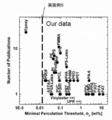
- the percolation threshold value of the carbon nanotube composite material of the present invention described in Example 4 and Example 5 described later is 0.048% by weight, which is extremely small as compared with the conventional report.
- FIG. 3 shows a comparison between the percolation threshold of the carbon nanotube composite material reported in the past literature (J. Kovacs and W. Bauhofer Composite Science and Technology 69, 1486-1498 (2009)) and the percolation threshold of the present invention.
- the carbon nanotube composite material of the present invention has a very small percolation threshold as compared with the conventional carbon nanotube composite material.
- the percolation threshold of the carbon nanotube composite material 100 of the present invention is preferably such that the blending amount is 0.0001 wt% or more, 0.2 wt% or less, more preferably 0.1 wt% or less, more preferably 0.05% by weight or less.
- the CNT group 15 in which the carbon nanotubes 10 are non-uniformly dispersed in the matrix 30 is observed.
- the CNT group 15 having a non-uniform shape in plan can be defined by fractal dimension analysis.
- the CNT group 15 has a fractal dimension of 1.7 or more.
- the fractal dimension of an infinitely sized cluster is 91/48 (1.895) in two dimensions, and 2.5 in three dimensions.
- the carbon nanotubes having a large aspect ratio efficiently come into contact with each other to form a continuous conductive path. Therefore, the fractal dimension of the conductive region is two-dimensional. It becomes close to 1.895 which is a fractal dimension forming an infinite size cluster.
- a continuous conductive path is formed by using the carbon nanotubes 10 having a large aspect ratio, so that the CNT group 15 can be formed with a small amount of carbon nanotubes added.
- Conductivity can be imparted with a fractal dimension of 1.66 or more, more preferably 1.7 or more.
- the fractal dimension analysis is performed using an optical microscope image of a cross section of the carbon nanotube composite material 100 using ImageJ, which is an open source image processing software, and FracLac, which is a plug-in for fractal dimension analysis. it can.
- ImageJ an open source image processing software
- FracLac a plug-in for fractal dimension analysis.
- LCFD Local Connected Fractal Dimension
- the carbon nanotube composite material 100 of the present invention is 10 ⁇ 11 S / cm or more, more preferably 10 ⁇ 10 S / cm or more, further preferably 10 ⁇ 9 S / cm or more, further preferably 10 ⁇ 7 S / cm or more, More preferably, it has a conductivity of 10 ⁇ 6 S / cm or more, more preferably 10 ⁇ 5 S / cm or more, more preferably 10 ⁇ 4 S / cm or more.
- the upper limit of the conductivity of the carbon nanotube composite material is not particularly limited, but it is difficult to exceed the carbon conductivity of 10 5 S / cm.
- the preferable amount of carbon nanotubes in the carbon nanotube composite material 100 of the present invention is more than the percolation threshold when the mass of the entire carbon nanotube composite material is 100% by weight.
- it is 0.0001% by weight or more, and 5% by weight or less, more preferably 1% by weight or less, more preferably 0% from the viewpoint of not impairing physical properties of the base material (matrix). .5% by weight or less, more preferably 0.2% by weight or less, and still more preferably 0.1% by weight or less.
- the base material region 35 where the carbon nanotubes of the carbon nanotube composite material of the present invention are not observed does not exist.
- the carbon nanotube composite material 100 of the present invention has high conductivity with a small blending amount. In general, it is extremely difficult to produce a conductive composite material having high conductivity with a small amount.
- the compounding quantity of the percolation threshold of the carbon nanotube composite material 100 manufactured with the manufacturing method of this invention, and the electroconductivity in a percolation threshold are shown.
- the points ⁇ and ⁇ are other examples of single-walled carbon nanotubes and multi-walled carbon nanotubes reported in past literature.
- the carbon nanotube composite material 100 manufactured by the manufacturing method of the present invention exhibits a percolation threshold with a very small amount of orientation compared to other examples, and the conductivity at the percolation threshold is other than that of the other examples. There is a feature that it is extremely high compared to the case.
- the carbon nanotube composite material 100 of the present invention preferably has a conductivity of 10 ⁇ 7 S / cm or more at a blending amount of 1% by weight or less, more preferably a conductivity of 10 ⁇ 4 S / cm or more at a blending amount of 1% by weight or less.
- the conductivity is 10 ⁇ 7 S / cm or more, more preferably when the amount is 0.5% by weight or less, the conductivity is 10 ⁇ 4 S / cm or more, and more preferably the amount is 0.2% by weight.
- conductive 10 -7 S / cm or higher more preferably the amount 0.2% by weight or less of a conductive 10 -4 S / cm or higher, more preferably the amount of 0.1 wt% or less of a conductive 10 - 7 S / cm or higher, more preferably has a higher conductivity 10 -7 S / cm at the amount 0.05 wt% or less.
- a conductive composite material having a high conductivity with a small blending amount is a product obtained for the first time in the present invention.
- the carbon nanotube composite material 100 of the present invention Since the carbon nanotube composite material 100 of the present invention has a low percolation threshold and a book material region, the carbon nanotube composite material 100 has the characteristics of maintaining the physical properties of the base material in a blending amount having conductivity.
- FIG. 5 shows changes in electrical conductivity and Young's modulus of the fluororubber composite material with respect to the blending amount of CNT.
- the conductivity of the CNT composite material starts to increase from about 2 ⁇ 10 ⁇ 2 wt% of the CNT content, but the Young's modulus starts to increase from around 10 wt% of the CNT content. This means that between 2 ⁇ 10 ⁇ 2 wt% and 10 wt%, the rubber inherently soft characteristic is not lost while having conductivity.
- the electrical conductivity of the carbon nanotube used for the carbon nanotube composite material of the present invention is 1 S / cm or more, more preferably 10 S / cm or more, and further preferably 50 S / cm or more. Carbon nanotubes having such conductivity are preferred for obtaining a highly conductive carbon nanotube composite material. There is no particular upper limit for the conductivity of carbon nanotubes, but it is difficult to exceed 10 5 S / cm, which is the conductivity of carbon.
- the characteristics of the carbon nanotube used for the carbon nanotube composite material of the present invention can be evaluated by extracting only the carbon nanotube from the carbon nanotube composite material, for example, backing paper. For extraction, a known means such as dissolving a matrix using a solvent can be appropriately used.
- the length of the carbon nanotube used for the carbon nanotube composite material of the present invention is 0.1 ⁇ m or more, more preferably 0.5 ⁇ m or more, and further preferably 1 ⁇ m or more. Since such carbon nanotubes have a large aspect ratio and come into contact with each other efficiently, a continuous conductive path can be formed with a small amount of added carbon nanotubes.
- the average diameter of the carbon nanotube used for the carbon nanotube composite material of the present invention is in the range of 1 nm to 30 nm, preferably in the range of 1 nm to 10 nm. If the average diameter is too small, the cohesiveness is too strong to disperse. On the other hand, if the average diameter is too large, the contact resistance between the carbon nanotubes increases, so that formation of a conductive path having high conductivity is hindered.
- the average diameter of the carbon nanotubes used in the carbon nanotube composite material of the present invention is determined based on the transmission electron microscope (hereinafter referred to as TEM) image of the aligned carbon nanotube aggregate before being dispersed in the matrix. The diameter, that is, the diameter is measured to create a histogram, which is obtained from this histogram.
- TEM transmission electron microscope
- the carbon purity of the carbon nanotube used in the carbon nanotube composite material of the present invention is preferably 90% by weight or more, more preferably 95% by weight or more, and still more preferably 98% by weight or more. It is. Such high-purity carbon nanotubes are suitable for obtaining high conductivity with a small amount of addition because the amount of impurities with little contribution to the formation of the conductive path is small. Carbon purity indicates what percentage of the carbon nanotube weight is composed of carbon, and the carbon purity of the carbon nanotube used in the carbon nanotube composite material of the present invention is determined from elemental analysis using fluorescent X-rays.
- a carbon nanotube composite material including a carbon nanotube in which at least one peak is observed in a region of 110 ⁇ 10 cm ⁇ 1 , 190 ⁇ 10 cm ⁇ 1 , and 200 cm ⁇ 1 or more by Raman spectroscopy at a wavelength of 633 nm is an effect of the present invention. It is suitable for obtaining.
- the structure of the carbon nanotube can be evaluated by Raman spectroscopy. There are various laser wavelengths used in the Raman spectroscopic analysis, but here, wavelengths of 532 nm and 633 nm are used.
- the region below 350 cm ⁇ 1 in the Raman spectrum is called a radial breathing mode (hereinafter referred to as RBM), and the peak observed in this region correlates with the diameter of the carbon nanotube.
- RBM radial breathing mode
- the carbon nanotube according to the present invention at least one peak is observed in the region of 110 ⁇ 10 cm ⁇ 1 , 190 ⁇ 10 cm ⁇ 1 , and 200 cm ⁇ 1 or more by Raman spectroscopy at a wavelength of 633 nm, It is composed of carbon nanotubes having a diameter. Therefore, the interaction for forming and holding the carbon nanotube bundle is relatively weak. Therefore, carbon nanotubes can be easily dispersed in the matrix, and a carbon nanotube composite material having high conductivity can be obtained with a small amount of carbon nanotubes.
- the carbon nanotubes used for the carbon nanotube composite material of the present invention are preferable because the fewer defects in the graphene sheet, the better the quality and the higher the conductivity.
- the defect of this graphene sheet can be evaluated by Raman spectroscopy.
- Raman spectroscopy There are various laser wavelengths used in the Raman spectroscopic analysis, but here, wavelengths of 532 nm and 633 nm are used.
- the Raman shift observed near 1590 cm ⁇ 1 is called the G band derived from graphite
- the Raman shift observed near 1350 cm ⁇ 1 is called the D band derived from defects in amorphous carbon or graphite.
- the height ratio (G / D ratio) of G band and D band by Raman spectroscopic analysis is used.
- a carbon nanotube having a higher G / D ratio has a higher degree of graphitization and higher quality.
- a wavelength of 532 nm is used.
- a higher G / D ratio is better, but if it is 3 or more, the carbon nanotubes contained in the conductive material have a sufficiently high conductivity, which is preferable for obtaining a carbon nanotube composite material having high electrical conductivity.
- the G / D ratio is preferably 4 or more and 200 or less, and more preferably 5 or more and 150 or less.
- Raman spectroscopy may vary depending on sampling. Therefore, at least three places and another place are subjected to Raman spectroscopic analysis, and an arithmetic average thereof is taken.
- the carbon nanotube used for the carbon nanotube composite material of the present invention is preferably a single-walled carbon nanotube. Since single-walled carbon nanotubes have a lower density than multi-walled carbon nanotubes, the length of carbon nanotubes per weight is increased, which is preferable for obtaining high conductivity with a small amount of addition.
- the matrix used for the carbon nanotube composite material of the present invention is preferably an elastomer. Elastomers are preferred because they have excellent deformability.
- the elastomer applicable to the carbon nanotube composite material of the present invention is flexible, conductive and durable.
- the elastomer includes natural rubber (NR), epoxidized natural rubber (ENR), styrene-butadiene.
- SBR Rubber
- NBR nitrile rubber
- EPR ethylene propylene rubber
- IIR butyl rubber
- CIIR chlorobutyl rubber
- acrylic rubber ACM
- silicone rubber Q
- fluorine Elastomers such as rubber (FKM), butadiene rubber (BR), epoxidized butadiene rubber (EBR), epichlorohydrin rubber (CO, CEO), urethane rubber (U), polysulfide rubber (T), olefinic (TPO), poly Vinyl chloride (TPVC), polyester (T EE), polyurethane (TPU), polyamide (TPEA), one or more can be mentioned selected from thermoplastic elastomers such as styrene (SBS).
- the elastomer used in the carbon nanotube composite material of the present invention is preferably a highly polar elastomer that easily generates free radicals during elastomer kneading, such as natural rubber (NR) or nitrile rubber (NBR).
- NR natural rubber
- NBR nitrile rubber
- One or more selected from the group may be cross-linked.
- thermosetting resin examples include unsaturated polyesters, vinyl esters, epoxies, phenols (resol type), urea melamines, polyimides, copolymers thereof, modified products, and resins blended in two or more types. Can be used. Further, in order to further improve the impact resistance, a resin obtained by adding an elastomer or a rubber component to the thermosetting resin may be used.
- thermoplastic resin examples include polyethylene terephthalate (PET), polybutylene terephthalate (PBT), polytrimethylene terephthalate (PTT), polyethylene naphthalate (PEN), polyester such as liquid crystal polyester, polyethylene (PE), polypropylene ( PP), polyolefins such as polybutylene, styrene resins, polyoxymethylene (POM), polyamide (PA), polycarbonate (PC), polymethylene methacrylate (PMMA), polyvinyl chloride (PVC), polyphenylene sulfide ( PPS), polyphenylene ether (PPE), modified PPE, polyimide (PI), polyamideimide (PAI), polyetherimide (PEI), polysulfone (PSU), polyethersulfone , Polyketone (PK), polyetherketone (PEK), polyetheretherketone (PEEK), polyetherketoneketone (PEKK), polyarylate (PAR), polyethernitrile (PEN), phenolic resin
- the matrix used in the carbon nanotube composite material of the present invention is particularly preferably a fluororesin or fluororubber. This is because the affinity between the fluororesin and CNT is high, and CNT can be dispersed well.
- Fluororesin includes polytetrafluoroethylene, polychlorotrifluoroethylene polyvinylidene fluoride, polyvinyl fluoride, perfluoroalkoxy fluororesin, ethylene tetrafluoride / hexafluoropropylene copolymer, ethylene / tetrafluoroethylene copolymer , Ethylene / chlorotrifluoroethylene copolymer, or a mixture thereof can be preferably used.
- the cross-linking agent varies depending on the type of the elastomer described above.
- an isocyanate group-containing cross-linking agent isocyanate, blocked isocyanate, etc.
- a sulfur-containing cross-linking agent sulfur, etc.
- a peroxide cross-linking agent peroxide, etc.
- Hydrosilyl group-containing crosslinking agents hydrosilyl curing agents
- urea resins such as melamine, epoxy curing agents, polyamine curing agents, and photocrosslinking agents that generate radicals by energy such as ultraviolet rays and electron beams.
- the carbon nanotube composite material of the present invention includes, for example, an ionic conductive agent (surfactant, ammonium salt, inorganic salt), plasticizer, oil, cross-linking agent, cross-linking accelerator, anti-aging agent.
- an ionic conductive agent surfactant, ammonium salt, inorganic salt
- plasticizer oil
- cross-linking agent cross-linking accelerator
- anti-aging agent anti-aging agent.
- a flame retardant, a colorant, and the like may be used as appropriate.
- the carbon nanotube composite material of the present invention Since the carbon nanotube composite material of the present invention has high conductivity and does not impair the inherent properties of the matrix, it can be used as an antistatic material or the like.
- the carbon nanotube composite material of the present invention is obtained by dispersing carbon nanotubes having the above-described characteristics in a matrix.
- the carbon nanotube used for the carbon nanotube composite material of the present invention can be manufactured by a chemical vapor deposition method using a manufacturing apparatus 500 shown in FIG. In this manufacturing method, the first gas containing the raw material gas and the second gas containing the catalyst activation material are supplied from separate gas supply pipes, and the gas flow path constituted by the separate pipes in the heating region is allowed to flow.
- the raw material gas and the catalyst activation material are mixed and supplied without reacting, and the first gas and the second gas are mixed and reacted in the vicinity of the catalyst layer. Since it can be brought into contact with the catalyst layer, it is very efficient and can be continuously grown for a long time, usually in about 10 minutes, so it is very long and highly pure.
- Single-walled carbon nanotubes can be synthesized, which is suitable for obtaining the composite material of the present invention.
- a base material 501 eg, a silicon wafer
- a catalyst layer 503 eg, an alumina-iron thin film
- the atmospheric gas supplied through the one gas flow path 545 is filled.
- the base material 501 is disposed so that the surface of the catalyst layer 503 and the first gas flow path 545 and the second gas flow path 547 are generally perpendicular to each other so that the source gas is efficiently supplied to the catalyst.
- a reducing gas for example, hydrogen
- the interior of the synthesis furnace 510 is heated to a predetermined temperature (for example, 750 ° C.), This state is maintained for a desired time.
- the catalyst layer 503 is reduced to form fine particles having various sizes, and is adjusted to a state suitable as a catalyst for carbon nanotubes.
- each of the raw material gas and the catalyst activation material is disposed in the synthesis furnace 510. It supplies to the gas mixing area
- a raw material gas for example, ethylene
- These gases supplied from the first gas channel 545 and the second gas channel 547 form a gas flow directed in a direction substantially parallel to the surface of the catalyst layer 503 of the base material 1, and then the catalyst layer 503.
- the gas is mixed in the nearby gas mixing region 580 and supplied to the surface of the catalyst layer 503 on the substrate 501 in a predetermined amount.
- the raw material gas contained in the first gas undergoes a decomposition reaction while passing through the first gas flow path 545, and is in a state suitable for the production of carbon nanotubes. Further, by supplying from the second gas flow path 547, a predetermined amount of the catalyst activation material is supplied to the gas mixing region 580 without reacting with the source gas. Since the first gas and the second gas optimized in this way are mixed in the gas mixing region 580 and brought into contact with the catalyst layer 503, the growth is very high efficiency and normally deactivates in about 10 minutes. Can be performed continuously for a long time. Therefore, a very long carbon nanotube aggregate composed of single-walled carbon nanotubes with high purity can be efficiently manufactured at high speed and with high yield from the catalyst layer deposited on the substrate 501.
- the raw material gas contained in the first gas, the catalyst activation material contained in the second gas, the decomposition products thereof, the carbon impurities existing in the synthesis furnace 510, etc. remaining in the synthesis furnace 510 In order to suppress the adhesion of carbon to the carbon nanotube aggregate, only the atmospheric gas is allowed to flow from the first gas flow path 545.
- the aggregate of carbon nanotubes, the catalyst, and the substrate 501 are preferably cooled to 400 ° C. or lower, more preferably 200 ° C. or lower in a cooling gas environment.
- a cooling gas an inert gas supplied from the second gas supply pipe 43 is preferable, and nitrogen is particularly preferable from the viewpoints of safety, economy, purgeability, and the like.
- the carbon nanotube used for the carbon nanotube composite material of the present invention can be produced.
- the base material 501 (substrate) is a member capable of supporting a catalyst for growing carbon nanotubes on the surface thereof, and an appropriate material can be used as long as the shape can be maintained even at a high temperature of 400 ° C. or higher. Can do.
- a planar form such as a flat plate is preferable for producing a large amount of carbon nanotubes using the effects of the present invention.
- any suitable catalyst can be used as long as it has a proven record in the production of conventional carbon nanotubes. Specifically, iron, nickel, cobalt, molybdenum, and the like can be used. These chlorides and alloys may be further combined with or laminated with aluminium, alumina, titania, titanium nitride, or silicon oxide.
- the catalyst may be present in a range that has a proven record in the production of carbon nanotubes so far.
- the thickness is preferably 0.1 nm or more and 100 nm or less.
- the thickness is more preferably from 5 nm to 5 nm, particularly preferably from 0.8 nm to 2 nm.
- the reducing gas is a gas that has at least one effect of reducing the catalyst, promoting atomization in a state suitable for the growth of the carbon nanotubes of the catalyst, and improving the activity of the catalyst.
- the reducing gas for example, hydrogen, ammonia, water, a mixed gas thereof, or the like that has been used in the production of carbon nanotubes so far can be applied.
- the atmospheric gas (carrier gas) for chemical vapor deposition may be any gas that is inert at the growth temperature of carbon nanotubes and does not react with the growing carbon nanotubes.
- An active gas is preferable, and nitrogen, helium, argon, hydrogen, and a mixed gas thereof are preferable.
- Raw material As a raw material used for the production of carbon nanotubes, an appropriate substance can be used as long as it has a proven record in the production of conventional carbon nanotubes.
- the source gas hydrocarbons such as methane, ethane, propane, butane, pentane, hexane, heptane, propylene, ethylene, butadiene, polyacetylene and acetylene are suitable.
- a catalyst activator is added in the carbon nanotube growth step.
- a catalyst activator By adding a catalyst activator, the life of the catalyst can be extended and the activity can be increased. As a result, the production efficiency of carbon nanotubes and the purification can be promoted.
- the catalyst activation material may be any material that has an oxidizing power such as oxygen or sulfur and that does not cause significant damage to the carbon nanotubes at the growth temperature. Water, oxygen, carbon dioxide, carbon monoxide, Ethers and alcohols are preferred, but water that can be obtained very easily is particularly suitable.
- the raw material contains carbon and does not contain oxygen
- the catalyst activator contains oxygen
- the first gas containing the raw material gas is supplied into the synthesis furnace 510 via the first gas flow path 545
- the second gas containing the catalyst activation material for example, water
- the synthesis furnace 510 Through the synthesis furnace 510.
- the raw material gas undergoes a decomposition reaction while passing through the first gas flow path 545, and is in a state suitable for the production of carbon nanotubes.
- a predetermined amount of the catalyst activation material is supplied to the gas mixing region 580 without reacting with the source gas.
- the first gas and the second gas optimized in this way are mixed in the gas mixing region 580 and brought into contact with the catalyst layer 503, so that the growth is extremely high and normally deactivated in about 10 minutes. Can be performed continuously for a long time. Therefore, a very long and high-purity single-walled carbon nanotube can be synthesized, which is suitable for obtaining the composite material of the present invention.
- reaction temperature The reaction temperature for growing the carbon nanotubes is preferably 400 ° C. or higher and 1000 ° C. or lower. If it is less than 400 degreeC, the effect of a catalyst activation material will not express, but if it exceeds 1000 degreeC, a catalyst activation material will react with a carbon nanotube.
- the aggregate of carbon nanotubes is peeled off from the substrate 501 using a physical, chemical or mechanical method (S101).
- a peeling method for example, a method of peeling using an electric field, a magnetic field, centrifugal force, and surface tension, a method of peeling directly from the base material 501, a method of peeling from a substrate using pressure or heat, and the like are applicable. It is. Further, a method of peeling the carbon nanotube aggregate from the substrate 501 using a thin blade such as a cutter blade, or a method of sucking the carbon nanotube aggregate from the substrate 501 using a vacuum pump is preferable.
- a drying step is performed on the carbon nanotube aggregates that have been peeled off (S101).
- the dispersibility is increased, which is suitable for producing the carbon nanotube composite material according to the present invention.
- the carbon nanotubes constituting the carbon nanotube aggregate used in the carbon nanotube composite material of the present invention readily adsorb moisture in the atmosphere between the carbon nanotubes during storage and transportation in the atmosphere.
- moisture content adsorb
- the carbon nanotube drying step before the dispersion step, moisture contained in the carbon nanotubes can be removed and the dispersibility in the dispersion medium can be improved.
- the drying step for example, heat drying or vacuum drying can be used, and heat vacuum drying is preferably used.
- the separated carbon nanotube aggregate is preferably classified by a classification process (S103).
- the classification step is a step of obtaining a carbon nanotube aggregate having a uniform size by setting the size of the carbon nanotube aggregate to a predetermined range.
- the aggregate of carbon nanotubes peeled from the substrate 501 includes a large-sized aggregated synthetic product. These large aggregates of large-sized carbon nanotubes have different dispersibility, and therefore, the production of a stable dispersion is hindered. Therefore, if only the carbon nanotube aggregates that have passed through the net, filter, mesh, etc. and excluding the large aggregated carbon nanotube aggregates are used in the subsequent steps, it is preferable for obtaining a stable carbon nanotube dispersion.
- the classified carbon nanotube aggregate is preferably subjected to a pre-dispersion step before the next dispersion step (S105).
- the pre-dispersing step is a step of stirring and dispersing the carbon nanotube aggregate in a solvent.
- the carbon nanotube used in the carbon nanotube composite material of the present invention is preferably a dispersion method using a jet mill. However, by performing a pre-dispersion step, the jet mill is prevented from being clogged with carbon nanotubes. The dispersibility of the carbon nanotube can be improved. It is preferable to use a stirrer for the pre-dispersion step.
- a dispersion step is performed on the dispersion liquid of the carbon nanotube aggregate subjected to the pre-dispersion step (S107).
- a method of dispersing the carbon nanotube aggregate in the dispersion is preferable, and a jet mill is preferably used.
- a wet jet mill can be suitably used.
- a mixture in a solvent is fed as a high-speed flow from a nozzle arranged in a sealed state in a pressure vessel.
- the carbon nanotubes are dispersed by collision between opposing flows, collision with the vessel wall, turbulent flow caused by high-speed flow, shear flow, and the like.
- the treatment pressure in the dispersion step is preferably a value in the range of 10 MPa to 150 MPa.
- the carbon nanotube dispersion liquid thus dispersed can provide a highly stable and stable dispersion liquid while maintaining the excellent electrical characteristics, thermal conductivity, and mechanical properties of the carbon nanotubes.
- a matrix solution in which the matrix is dissolved in a solvent is prepared, added to the carbon nanotube dispersion, and sufficiently stirred to disperse the carbon nanotubes in the matrix (S109).
- the mass of the entire carbon nanotube composite material is 100% by weight, 0.0001% by weight to 5% by weight, more preferably 0.005% by weight.
- the carbon nanotube dispersion and the matrix solution are mixed so that the content is 2% by weight or less.
- the sufficiently mixed solution is poured into a mold such as a petri dish and dried at room temperature to solidify the carbon nanotube composite material (S111).
- the solidified carbon nanotube composite material is placed in a vacuum drying oven and dried to remove the solvent (S113).
- the drying temperature is a temperature at which the solvent can be sufficiently removed from the carbon nanotube composite material and the matrix is not deteriorated. Therefore, although it can be changed depending on the matrix used for the carbon nanotube composite material, for example, at about 80 ° C., the solvent is sufficiently removed and the matrix is not deteriorated.
- the solvent used for dissolving the carbon nanotube dispersion medium and matrix used in the carbon nanotube composite material of the present invention may be any organic solvent that can dissolve the matrix, and can be appropriately selected depending on the matrix used.
- organic solvent for example, toluene, xylene, acetone, carbon tetrachloride and the like can be used.
- MIBK methyl isobutyl ketone
- a dispersant may be added to the carbon nanotube dispersion.
- the dispersant is useful for improving the dispersibility and dispersion stabilization ability of the carbon nanotubes.
- the carbon nanotube composite material of the present invention that can exhibit high conductivity with a low amount of carbon nanotubes can be produced.
- Example 1 Manufacture of carbon nanotube aggregates
- a carbon nanotube aggregate was manufactured using the manufacturing apparatus 500 of FIG. 6 described above.
- a quartz tube such as a cylinder was used as the vertical synthesis furnace 510.
- a substrate holder 505 made of quartz was provided 20 mm downstream from the horizontal position of the center.
- a heating means 530 composed of a resistance heating coil provided around the synthesis furnace 510 and a heating temperature adjusting means are provided to define the heating region 31 in the synthesis furnace 510 heated to a predetermined temperature.
- a gas flow forming means 521 made of a heat-resistant alloy Inconel 600 having a cylindrical and flat hollow structure with a diameter of 78 mm was provided so as to communicate with the end of the first gas supply pipe 541 in the synthesis furnace 510.
- the first gas supply pipe 541 was connected in communication with the center of the gas flow forming means 521.
- the gas flow forming means 521 is arranged in the same plane substantially parallel to the surface of the catalyst layer of the base material 501, and the center of the base material 501 is arranged so as to coincide with the center of the gas flow forming means 521. It was done.
- the gas flow forming means 521 has a cylindrical shape having a hollow structure, and the dimensions are, for example, a cylindrical shape having an upper end diameter of 22 mm and a lower end diameter of 78 mm, and four pipes having a diameter of 32 mm. 557 connected.
- the second gas supply pipe 543 disposed so as to coincide with the center of the first gas supply pipe 541 extends so as to coincide with the center of the gas flow forming means 521 and coincides with the center of Diameter: 13 mm outlet was disposed.
- connection portion of the pipe 555 and the pipe 557 of the gas flow forming means 521 and the surface of the catalyst layer facing the pipe 555 was 150 mm.
- the first gas channel 545 is connected to the gas flow forming unit 521 and includes a turbulent flow preventing unit 523.
- the first gas flow path 545 includes four pipes 555 having a diameter of 32 mm arranged like a honeycomb structure made of the heat-resistant alloy Inconel 600, and the second gas flow path 547 coincides with the center of the four pipes 555.
- a pipe 557 having a diameter of 13 mm is provided.
- the first carbon weight flux adjusting means 571 includes a source gas cylinder 561 that is a carbon compound that is a source of carbon nanotubes, an atmosphere gas cylinder 563 that is a carrier gas of the source gas and the catalyst activation material, and a reducing gas cylinder 565 that reduces the catalyst.
- the supply amount of the source gas was controlled by connecting to the gas flow device and supplying the first gas supply pipe 541 while independently controlling the supply amount.
- the second carbon weight flux adjusting means 573 is configured by connecting the catalyst activation material cylinder 567 to a gas flow device and supplying the second gas supply pipe 543 to control the supply amount of the catalyst activation material.
- a Si base material (40 mm long ⁇ 40 mm wide) with a thermal oxide film having a thickness of 500 nm obtained by sputtering 30 nm of Al 2 O 3 as a catalyst and 1.8 nm of Fe was used.
- the base material 501 was carried onto the substrate holder 508 installed 20 mm downstream from the horizontal position at the center of the heating region 531 of the synthesis furnace 502.
- the substrate was placed in a horizontal direction.
- the catalyst and mixed gas flow paths on the substrate generally intersect perpendicularly, and the source gas is efficiently supplied to the catalyst.
- the synthesis furnace 510 while supplying a mixed gas (total flow rate: 2000 sccm) of He: 200 sccm and H 2 : 1800 sccm as the reducing gas from the first gas flow path 545, the synthesis furnace 510 with the furnace pressure set to 1.02 ⁇ 10 5 Pa. The temperature inside the synthesis furnace 510 was increased from room temperature to 830 ° C. over 15 minutes using the heating means 530. Further, while supplying 80 sccm of water as a catalyst activator from the second gas supply pipe 543, the substrate with catalyst was heated for 3 minutes while maintaining at 830 ° C. As a result, the iron catalyst layer was reduced to promote the formation of fine particles suitable for the growth of single-walled carbon nanotubes, and a large number of nanometer-sized catalyst fine particles having different sizes were formed on the alumina layer.
- a mixed gas total flow rate: 2000 sccm
- H 2 1800 sccm
- the temperature of the synthesis furnace 510 with the furnace pressure of 1.02 ⁇ 10 5 Pa (atmospheric pressure) is set to 830 ° C.
- the atmosphere gas He total flow ratio 89% (1850 sccm) from the first gas flow path 545
- the raw material Gas C 2 H 4 7% (150 sccm) of the total flow rate
- H 2 O-containing He relative humidity 23%): 4% (80 sccm) of the total flow rate as the catalyst activator from the second gas supply pipe 543 Feed for 10 minutes.
- total flow rate 4000 sccm was supplied from the first gas flow path 545 for 3 minutes to eliminate the remaining raw material gas, generated carbon impurities, and catalyst activator.
- the substrate was taken out from the synthesis furnace 510 to complete a series of single-walled carbon nanotube assembly manufacturing steps.
- the D band peak derived from the defect structure or the like is observed in the vicinity of 1340 cm ⁇ 1 , it indicates that the carbon nanotube contains a significant defect. Since the RBM mode due to a plurality of single-walled carbon nanotubes was observed on the low wavelength side (100 to 300 cm ⁇ 1 ), it can be seen that this graphite layer is a single-walled carbon nanotube. The G / D ratio was 8.6.
- the carbon purity of the carbon nanotube aggregate was determined from the result of elemental analysis using fluorescent X-rays. Elemental analysis of the aggregate of carbon nanotubes separated from the substrate by fluorescent X-ray revealed that the carbon weight percentage was 99.98%, the iron weight percentage was 0.013%, and other elements were not measured. From this result, the carbon purity was measured as 99.98%.
- a carbon nanotube aggregate is placed on one side of a mesh with an opening of 0.8 mm, sucked with a vacuum cleaner through the net, and the passing material is collected. From the carbon nanotube aggregate, large lumped carbon is collected. The aggregate of nanotubes was removed and classification was performed (classification process).
- the aggregate of carbon nanotubes was measured by the Karl Fischer reaction method (coulometric titration type trace moisture measuring device CA-200 type manufactured by Mitsubishi Chemical Analytech). After drying the aggregate of carbon nanotubes under predetermined conditions (maintained at 200 ° C. for 1 hour under vacuum), the vacuum is released in a glove box in a dry nitrogen gas stream, and about 30 mg of the aggregate of carbon nanotubes is taken out, and a moisture meter Moved to a glass boat. The glass boat moved to a vaporizer, where it was heated at 150 ° C. for 2 minutes, and the vaporized water was conveyed with nitrogen gas and reacted with iodine by the adjacent Karl Fischer reaction.
- the amount of water was detected from the amount of electricity required to generate an amount of iodine equal to the iodine consumed at that time.
- the aggregate of carbon nanotubes before drying contained 0.8% by weight of water.
- the aggregate of carbon nanotubes after drying was reduced to 0.3% by weight of water.
- 100 mg of the classified carbon nanotube aggregate was accurately weighed, put into a 100 ml flask (3 necks: for vacuum, for temperature control), held at vacuum for 200 hours and dried for 24 hours. After the drying was completed, 20 ml of dispersion medium MIBK (methyl isobutyl ketone) (manufactured by Sigma-Aldrich Japan) was injected in the state of heating and vacuum treatment to prevent the carbon nanotube aggregate from coming into contact with the atmosphere (drying step).
- MIBK methyl isobutyl ketone
- MIBK manufactured by Sigma Aldrich Japan
- a stir bar was placed in the beaker, the beaker was sealed with aluminum foil, and MIBK was not volatilized, and stirred at room temperature with a stirrer at 600 RPM for 24 hours.
- a wet jet mill (Nanojet Pal (registered trademark) JN10 manufactured by Joko) was passed through a 200 ⁇ m channel at a pressure of 60 MPa to disperse the aggregate of carbon nanotubes in MIBK.
- a carbon nanotube dispersion liquid of 033% by weight was obtained.
- the dispersion was further stirred with a stirrer at room temperature for 24 hours. At this time, the temperature of the solution was raised to 70 ° C. to volatilize MIBK to about 150 ml. The weight concentration of the carbon nanotubes at this time was about 0.075% by weight (dispersing step). In this way, a carbon nanotube dispersion according to the present invention was obtained.
- fluororubber (Daikin Industries, Daiel-G912) was used as the matrix.
- the total mass of the carbon nanotube composite material is 100% by weight
- 150 ml of the carbon nanotube dispersion liquid is added to 50 ml of the fluororubber solution so that the carbon nanotube content is 1%.
- the mixture was stirred at room temperature for 16 hours and concentrated to a total volume of about 50 ml.
- the sufficiently mixed solution was poured into a mold such as a petri dish and dried at room temperature for 12 hours to solidify the carbon nanotube composite material.
- the solidified carbon nanotube composite material was put in a vacuum drying furnace at 80 ° C. and dried for 24 hours to remove the solvent.
- the carbon nanotube composite material 200 of Example 1 was obtained (the shape of the sample is a circular sheet having a diameter of 77 mm and a thickness of about 300 ⁇ m).
- Example 2 As Example 2, a carbon nanotube composite material 210 prepared to have a carbon nanotube content of 0.25% was obtained using the same manufacturing method as in Example 1.
- Example 3 As Example 3, a carbon nanotube composite material 220 prepared so that the carbon nanotube content was 0.01 wt% was obtained using the same manufacturing method as in Example 1.
- Example 4 As Example 4, a carbon nanotube composite material 230 prepared using the same manufacturing method as in Example 1 so that the carbon nanotube content was 0.048 wt% was obtained. At this time, the carbon nanotube content of 0.048 wt% corresponds to the percolation threshold, and the volume conductivity of the carbon nanotube composite material at this time is 0.12 S / cm.
- Example 5 50 mg of a carbon nanotube aggregate produced by the same production method as in Example 1 was accurately weighed and put into a 100 ml flask (3 necks: for vacuum, for temperature control), and after reaching 200 ° C. under vacuum for 24 hours. Retained and dried. After the drying was completed, 100 ml of pure water and 10 mg of sodium deoxycholate were injected while being heated and vacuum-treated to prevent the carbon nanotube aggregate from being exposed to the atmosphere. In the dispersion step, a wet jet mill (Nanojet Pal (registered trademark) JN10, manufactured by Joko) was passed through a 200 ⁇ m flow path at a pressure of 60 MPa to disperse the aggregate of carbon nanotubes in pure water.
- a wet jet mill Neanojet Pal (registered trademark) JN10, manufactured by Joko
- a 0.033 wt% carbon nanotube dispersion was obtained.
- the dispersion was further stirred with a stirrer at room temperature for 24 hours. At this time, the temperature of the solution was raised to 70 ° C., and water was volatilized to about 150 ml. The weight concentration of the carbon nanotubes at this time was about 0.075% by weight (dispersing step). In this way, a carbon nanotube dispersion was obtained.
- fluororubber latex manufactured by Daikin Industries
- the carbon nanotube composite material When the total mass of the carbon nanotube composite material is 100% by weight, 150 ml of the carbon nanotube dispersion is added to 50 ml of the fluororubber solution so that the carbon nanotube content is 0.013% by weight, and the condition is about 300 rpm using a stirrer. Under stirring at room temperature for 16 hours, the mixture was concentrated until the total amount reached about 50 ml.
- the sufficiently mixed solution was poured into a mold such as a petri dish and dried at room temperature for 12 hours to solidify the carbon nanotube composite material.
- the solidified carbon nanotube composite material was put in a vacuum drying furnace at 80 ° C. and dried for 24 hours to remove the solvent.
- the carbon nanotube composite material 240 of Example 5 was obtained (the shape of the sample is a circular sheet having a diameter of 77 mm and a thickness of about 300 ⁇ m).
- Example 6 As Example 6, using Polystyrene (SPJ, manufactured by PS Japan) as a matrix, similarly to the method of Example 1, a carbon nanotube composite material 250 prepared to have a carbon nanotube content of 0.1% by weight was obtained. .
- SPJ Polystyrene
- Example 7 As Example 7, a carbon nanotube composite material 260 prepared using PMMA (Sumipex, manufactured by Sumitomo Chemical Co., Ltd.) as a matrix and having a carbon nanotube content of 0.1% by weight was obtained in the same manner as in Example 1. .
- Example 8 As Example 8, acrylonitrile-butadiene-styrene copolymer synthetic resin (ABS resin) (manufactured by Toray Industries, Inc.) was used, and the carbon nanotube content was adjusted to 0.1% by weight in the same manner as in the production method of Example 1. A carbon nanotube composite material 270 was obtained.
- ABS resin acrylonitrile-butadiene-styrene copolymer synthetic resin
- Example 9 carbon prepared using an acrylonitrile-butadiene-styrene copolymer synthetic resin (ABS resin) (manufactured by Toray Industries, Inc.) as a matrix was prepared so that the carbon nanotube content was 1% in the same manner as in Example 1. A nanotube composite material 280 was obtained.
- ABS resin acrylonitrile-butadiene-styrene copolymer synthetic resin
- Example 10 As Example 10, polycarbonate (PC) (manufactured by Teijin Chemicals Ltd.) was used, and a carbon nanotube composite material 290 prepared so that the carbon nanotube content was 1% by weight was obtained in the same manner as in the method of Example 1.
- PC polycarbonate
- Teijin Chemicals Ltd. Teijin Chemicals Ltd.
- Example 11 carbon prepared by using Adelenka EP-4500 and Adeka Hardener EH (manufactured by ADEKA) as an epoxy resin as a matrix was prepared so that the carbon nanotube content was 1% by weight in the same manner as in Example 1. A nanotube composite material 300 was obtained.
- Comparative Example 1 Accurately weigh 50 mg of the carbon nanotube aggregate by this production method, put it into a 100 ml flask (3 necks: for vacuum, for temperature control), and hold it for 24 hours after reaching 200 ° C. under vacuum and let it dry. It was. After the drying was completed, 100 ml of dispersion medium MIBK (methyl isobutyl ketone) (manufactured by Sigma-Aldrich Japan) was injected in the state of heating and vacuum treatment to prevent the carbon nanotube aggregate from coming into contact with the atmosphere. To this was added 950 mg of fluororubber (Daikin Kogyo, Daiel-G912) to make 300 ml.
- MIBK methyl isobutyl ketone
- a stir bar was placed in the beaker, the beaker was sealed with aluminum foil, and MIBK was not volatilized, and stirred at room temperature with a stirrer at 600 RPM for 24 hours. Thereafter, the solvent was completely volatilized by maintaining at 80 ° C. These were pre-dried at 80 ° C. for 12 hours. Next, 1000 mg of this pre-dried sample and 4000 mg of fluororubber were put into a micro-type high shear molding machine so that the carbon nanotube content of the molded product was 1%, and the gap and the internal feedback screw inner diameter were 1-2 mm, It was set to 2.5 ⁇ , heated and melted at 180 ° C.
- Comparative Example 2 As Comparative Example 2, a carbon nanotube composite material 910 prepared to have a carbon nanotube content of 0.025% was obtained using the same production method as in Comparative Example 1.
- Comparative Example 3 As Comparative Example 3, a single-walled carbon nanotube (manufactured by Unidym) synthesized by HiPco (High-pressure carbon monoxide process) was used, and the carbon nanotube content was adjusted to 1% in the same manner as in Example 1. Carbon nanotube composite material 930 was obtained.
- Typical characteristics of a carbon nanotube aggregate (hereinafter referred to as HiPco) synthesized by the HiPco method are a length of 1 ⁇ m or less and an average diameter of 0.8 to 1.2 nm.
- FIG. 8 is a scanning electron microscope image (hereinafter referred to as SEM image) of a cross section of the carbon nanotube composite material 200 of Example 1.
- FIG. 9A is an optical microscope image of a cross section of the carbon nanotube composite material 200 of Example 1
- FIG. 9B is a laser microscope image.
- 10 and 11 show optical microscope images of a cross section of the carbon nanotube composite material 210 of Example 2
- FIG. 10 (a) is 500 times magnification
- FIG. 10 (b) is 1000 times magnification
- FIG. The magnification is 2000 times
- FIG. 10B shows the magnification of 3000 times
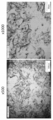
- 13 and 13 show optical microscope images of the cross section of the carbon nanotube composite material 220 of Example 3
- FIG. 12 (a) is 1000 times magnification
- FIG. 12 (b) is 2000 times magnification
- FIG. 5000 times are shown respectively. Note that the black granular substance observed in FIGS.
- FIG. 12 and 13 is a black pigment when the carbon nanotube composite material 220 of Example 3 is colored black.
- 14A is an optical microscope image of a cross section of the carbon nanotube composite material 230 of Example 4
- FIG. 14B is an optical microscope image of a cross section of the carbon nanotube composite material 240 of Example 5.
- FIG. FIG. 15 shows an optical microscope image of a cross section of the carbon nanotube composite material 230 of Example 4.
- FIG. 15A is a magnification of 3000 times
- FIG. 15B is a magnification of 2000 times
- FIG. 1000 times and FIG. 15 (d) show the magnification of 2000 times, respectively.
- FIG. 16 shows an optical microscope image of a cross section of the carbon nanotube composite material 240 of Example 5, FIG.
- FIG. 16 (a) is 2000 times magnification
- FIG. 16 (b) is 1000 times magnification
- FIG. 16 (c) is 3000 times magnification
- FIG. 16D shows the magnification of 1000 times. Although not shown, similar results were observed in Examples 6-11.
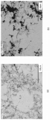
- FIG. 17 shows an optical microscope image of the carbon nanotube composite material 900 of Comparative Example 1.
- FIG. 18 shows an optical microscope image of the carbon nanotube composite material 910 of Comparative Example 2.
- FIG. 19 shows an SEM image of the carbon nanotube composite material 930 of Comparative Example 3.
- the portions that appear black each indicate the CNT group 15 composed of a plurality of carbon nanotubes, and the portions that appear white indicate the base material region 35.
- the carbon nanotube composite materials of Examples 1 to 5 (same as in Examples 6 to 11), the carbon nanotubes 10 are non-uniformly dispersed in the matrix 30 and the CNT group 15 including a plurality of CNTs 10 is obtained. It can be seen that there are a plurality of base material regions 35 where the carbon nanotubes 10 are not observed with a microscope, and a sea island structure formed by the base material region 35 and the CNT group 15 is provided.
- the first to eleventh embodiments as shown in FIG.
- the CNT group 15 in which a plurality of CNTs 10 are aggregated includes an aggregation unit 11 and a discrete unit 13, and the aggregation unit 11a and the aggregation unit 11b are , Have a discrete structure.
- the carbon nanotube composite material includes a base material region 35 and a CNT group 15 having a size of 20 ⁇ m. Since the CNT group 15 forms a continuous conductive path, excellent conductivity is imparted.
- the CNT group 15 that continuously connects the upper end and the lower end and / or the left end and the right end of the image in a 300 ⁇ m square region of the 1000 ⁇ optical microscope image.
- the carbon nanotube composite materials according to Examples 1 to 11 have a base material region 35 surrounded by the CNT group 15 with a blending amount of 1.0% by weight or less, and the base material surrounded by the CNT group 15 The region size of the region 35 is 10 ⁇ m or more.
- FIG. 20 is a diagram showing Raman mapping of the carbon nanotube composite material 200 of the first embodiment.
- the Raman spectrum measured at a wavelength of 633 nm does not depend on the matrix in the carbon nanotube composite material for the RBM and G / D ratio, and the carbon in the carbon nanotube composite material. It has been shown to be an excellent indicator by which nanotubes can be evaluated. In the measurement at a wavelength of 532 nm, the Raman spectrum was dependent on the type of matrix used for the carbon nanotube composite material.
- FIG. 20A is an optical microscopic image showing a region subjected to Raman mapping. Numbers 1, 5 to 8 in FIG.
- FIG. 20A indicate the CNT group 15, and numbers 2 to 4 indicate the base material region 35.
- FIG. 20 (b) shows the Raman spectra of the parts numbered 1 and 5 to 8 in FIG. 20 (a)
- FIG. 20 (c) shows the Raman spectra of the parts numbered 2 to 4 in FIG. 20 (a).
- site recognized as a CNT group 15 in the optical microscope image is within the range 1560 cm -1 or 1600 cm -1
- the following Raman spectroscopic analysis of wavelength 633nm in the Raman spectrum on the graph at the peak (visual A remarkable inflection point and / or a protrusion of 500% or more with respect to the baseline strength).
- the maximum peak intensity in the range Raman spectroscopic analysis of wavelength 633nm of 1560 cm -1 or 1600 cm -1 The following CNT groups 15, 1560 cm -1 or more in Raman spectroscopic analysis of wavelength 633nm of the base material region 35 1600 cm -1
- the ratio with the maximum peak intensity within the following range exceeds the measurement limit.
- the measurement limit differs depending on the noise level of the Raman spectrum and the background, but is estimated to be about 1000 in this measurement.
- similar results were obtained in Examples 2 to 11. From this result, it was found that the carbon nanotubes 10 were non-uniformly dispersed in the matrix 30 in the carbon nanotube composite material of the example.
- Carbon nanotube composite material 900 of Comparative Example 1 as shown in FIG. 21, the 10 points all measured, similar peaks at 1560 cm -1 or 1600 cm -1 in the following ranges are observed in Raman spectroscopic analysis of wavelength 633nm This shows that the carbon nanotubes are uniformly dispersed in the matrix.
- the blending amount is 0.1% by weight or less, and the region size is 10 ⁇ m or more.
- the region size is 10 ⁇ m or more.
- FIG. 23 is a diagram showing the analysis result of the fractal dimension of the carbon nanotube composite material.
- the fractal dimension analysis we used ImageJ, an open source image processing software, and FracLac Ver. 2.5, a plug-in for fractal dimension analysis. From this result, in the carbon nanotube composite material 200 of Example 1, it was shown that the CNT group 15 had a fractal dimension of 1.831 or more on average. Therefore, in the carbon nanotube composite material 200 having such a fractal dimension, the carbon nanotube groups can be efficiently brought into contact with each other to form a continuous conductive path, thereby imparting excellent conductivity.
- FIG. 22 shows the fractal dimensions of Examples 2 to 11 and Comparative Examples 1 to 3 measured in the same manner. While the fractal dimension of the example is 1.7 or more, the fractal dimension of the comparative example is 1.6 units, and it is inferred that the formation rate of the continuous conductive path is low.
- the carbon nanotube composite material of Example 1 has a conductivity four orders of magnitude higher than the carbon nanotube composite material of Comparative Example 3. Show. Accordingly, a carbon nanotube composite material in which at least one peak is observed in the region of 110 ⁇ 10 cm ⁇ 1 , 190 ⁇ 10 cm ⁇ 1 , and 200 cm ⁇ 1 or more in Raman spectroscopy at a wavelength of 633 nm has high conductivity. I understand that.
- G / D ratio The G / D ratios for Examples 1 to 11 and Comparative Examples 1 to 3 are summarized in FIG.
- the carbon nanotube composite material of the example has a G / D ratio of 3 or more.
Landscapes
- Chemical & Material Sciences (AREA)
- Engineering & Computer Science (AREA)
- Physics & Mathematics (AREA)
- Medicinal Chemistry (AREA)
- Polymers & Plastics (AREA)
- Organic Chemistry (AREA)
- Chemical Kinetics & Catalysis (AREA)
- Health & Medical Sciences (AREA)
- Materials Engineering (AREA)
- Nanotechnology (AREA)
- Dispersion Chemistry (AREA)
- Spectroscopy & Molecular Physics (AREA)
- Crystallography & Structural Chemistry (AREA)
- Inorganic Chemistry (AREA)
- Manufacturing & Machinery (AREA)
- General Physics & Mathematics (AREA)
- Condensed Matter Physics & Semiconductors (AREA)
- Composite Materials (AREA)
- Compositions Of Macromolecular Compounds (AREA)
- Carbon And Carbon Compounds (AREA)
Abstract
低添加量のカーボンナノチューブで高導電性を発揮できるカーボンナノチューブ複合材料を実現する。本発明のカーボンナノチューブ複合材料は、カーボンナノチューブをマトリックス中に分散してなるカーボンナノチューブ複合材料であって、複数のカーボンナノチューブより構成されるカーボンナノチューブ群と母材領域とを備え、カーボンナノチューブの配合量が0.0001重量%以上、1.0重量%以下で、カーボンナノチューブ複合材料の導電率が10-7S/cm以上であることを特徴とするカーボンナノチューブ複合材料である。
Description
本発明は、カーボンナノチューブをマトリックス中に分散させたカーボンナノチューブ複合材料に関する。
ポリマフォームおよびエラストマーに導電性フィラーを配合した、カーボンナノチューブ複合材料は各種の用途、たとえば、電子商品、コンピュータ、医用機器などにおいて、電磁遮蔽および/または静電気放散をさせるためのガスケットやシールとして、広く用いられている。過去においては通常、金属やカーボンブラックなどの微粒子を使用して導電性を与えていた。
しかしながら、このような、従来の導電フィラーは、微粒子形状のものが多く、導電性をマトリックスに付与するためには、添加量を多くする必要があった。一方、導電性フィラーの添加量を多くすると、カーボンナノチューブ複合材料は、例えば剛直な材料となり、マトリックスが本来備える特性が損なわれるという問題があった。
電子部品の小型化と、プラスチック部品の使用が進むにつれて、特に民生用電子機器では、より低添加量でマトリックスに導電を付与することが必要とされてきている。そこで、導電性に優れ、アスペクト比が高い、一次元形状のカーボンナノチューブが導電性フィラーとして着目されている。
しかしながら、カーボンナノチューブは、ファンデルワールス力により凝集しやすい。このため、カーボンナノチューブをエラストマー等のマトリックス中に配合すると、カーボンナノチューブが束状に凝集してしまい、均一に分散させることは難しい。そこで、カーボンナノチューブの凝集を解き、分散性を向上させる方法が、いくつか紹介されている(例えば、特許文献1)。
このようなカーボンナノチューブをマトリックスに均一に分散させる技術により、カーボンナノチューブを用いたカーボンナノチューブ複合材料が開発されてきた。例えば、中心部位から炭素繊維が三次元的(放射状)に延びているカーボンナノチューブをエラストマー中に配合すると、特定のカーボンナノチューブが、その三次元的な形状に由来し、エラストマー中で均一に分散する結果、エラストマー全体に連続的な導電路(導電パス)が形成され、導電性に優れた柔軟電極が実現されている(特許文献2)。
また、カーボンナノチューブ、イオン性液体、及びイオン性液体と混和性を有するゴムからなるカーボンナノチューブゴム組成物を含むカーボンナノチューブ複合材料は、電子回路の構成材料として用いるのに十分な導電性と通常のゴム材料にも劣らない弾性を有し、フレキシブルエレクトロニクスの実現が可能となる伸長可能なエレクトロニクスデバイスを与えることのできるカーボンナノチューブゴム、カーボンナノチューブゴムペースト、およびペーストをゴム基材とした導電性材料が開発された(非特許文献1)。しかし、これらの従来技術によるカーボンナノチューブ複合材料は、カーボンナノチューブの添加量を多くしないと導電性を付与できないという問題があった。
Tsuyoshi Sekitani et al, A Rubberlike Stretchable Active Matrix Using Elastic Conductors, SCIENCE, 2008.9.12, vol.321, p.1468-1472
本発明は、上記の如き従来技術の問題点を解決し、低添加量のカーボンナノチューブで高導電性を発揮できるカーボンナノチューブ複合材料を実現することを課題とする。
本発明の一実施形態によると、カーボンナノチューブをマトリックス中に分散してなるカーボンナノチューブ複合材料であって、複数のカーボンナノチューブより構成されるカーボンナノチューブ群と母材領域とを備え、カーボンナノチューブの配合量が0.0001重量%以上、1.0重量%以下で、カーボンナノチューブ複合材料の導電率が10-7S/cm以上であることを特徴とするカーボンナノチューブ複合材料が提供される。
前記カーボンナノチューブ群の波長633nmのラマン分光分析における1560cm-1以上1600cm-1以下の範囲内での最大ピーク強度と、前記母材領域の波長633nmのラマン分光分析で1560cm-1以上1600cm-1以下の範囲内における最大ピーク強度との比が5以上であってもよい。
また、本発明の一実施形態によると、カーボンナノチューブをマトリックス中に分散してなるカーボンナノチューブ複合材料であって、複数のカーボンナノチューブより構成されるカーボンナノチューブ群と母材領域を備え、前記カーボンナノチューブ群は、波長633nmのラマン分光分析で1560cm-1以上1600cm-1以下の範囲内にピークを有し、前記母材領域は、波長633nmのラマン分光分析で1560cm-1以上1600cm-1以下の範囲内にピークを有さないことを特徴とするカーボンナノチューブ複合材料が提供される。
前記カーボンナノチューブ複合材料が、10-11S/cm以上よりも大きい導電率を有する。
前記カーボンナノチューブ複合材料において、前記カーボンナノチューブ群は、フラクタル次元が1.7以上を備える。
前記カーボンナノチューブ複合材料において、前記カーボンナノチューブの配合量は、前記カーボンナノチューブ複合材料全体の質量を100重量%とした場合の0.0001重量%以上5重量%以下である。
前記カーボンナノチューブ複合材料が10S/cm以上の導電性を有するカーボンナノチューブを含む。
前記カーボンナノチューブ複合材料において、前記カーボンナノチューブの長さは、0.1μm以上である。
前記カーボンナノチューブ複合材料において、前記カーボンナノチューブの平均直径は、1nm以上30nm以下である。
前記カーボンナノチューブ複合材料において、前記カーボンナノチューブの蛍光X線を用いた分析による炭素純度が90重量%以上である。
前記カーボンナノチューブ複合材料は、波長633nmのラマン分光分析で、110±10cm-1、190±10cm-1及び200cm-1以上の領域に少なくとも一つのピークが観測される。
前記カーボンナノチューブ複合材料において、共鳴ラマン散乱測定法の測定により得られるスペクトルで1560cm-1以上1600cm-1以下の範囲内での最大のピーク強度をG、1310cm-1以上1350cm-1以下の範囲内での最大のピーク強度をDとしたときに、G/D比が3以上である。
前記カーボンナノチューブ複合材料において、前記カーボンナノチューブが単層カーボンナノチューブである。
前記カーボンナノチューブ複合材料において、前記のマトリックスは、エラストマーである。
前記カーボンナノチューブ複合材料において、前記のエラストマーは、天然ゴム、エポキシ化天然ゴム、スチレン-ブタジエンゴム、ニトリルゴム、クロロプレンゴム、エチレンプロピレンゴム、ブチルゴム、クロロブチルゴム、アクリルゴム、シリコーンゴム、フッ素ゴム、ブタジエンゴム、エポキシ化ブタジエンゴム、エピクロルヒドリンゴム、ウレタンゴム、ポリスルフィドゴム、およびオレフィン系、ポリ塩化ビニル系、ポリエステル系、ポリウレタン系、ポリアミド系、スチレン系の熱可塑性エラストマーから選ばれる一種以上である。
前記カーボンナノチューブ複合材料において、前記のマトリックスは、樹脂である。
前記カーボンナノチューブ複合材料において、前記樹脂は、不飽和ポリエステル、ビニルエステル、エポキシ、フェノール(レゾール型)、ユリア・メラミン、ポリイミド、ポリエチレンテレフタレート、ポリブチレンテレフタレート、ポリトリメチレンテレフタレート、ポリエチレンナフタレート、液晶ポリエステル、ポリエチレン、ポリプロピレン、ポリブチレン、スチレン系樹脂、ポリオキシメチレン、ポリアミド、ポリカーボネート、ポリメチレンメタクリレート、ポリ塩化ビニル、ポリフェニレンスルフィド、ポリフェニレンエーテル、変性ポリフェニレンエーテル、ポリイミド、ポリアミドイミド、ポリエーテルイミド、ポリスルホン、ポリエーテルスルホン、ポリケトン、ポリエーテルケトン、ポリエーテルエーテルケトン、ポリエーテルケトンケトン、ポリアリレート、ポリエーテルニトリル、フェノール系樹脂、フェノキシ樹脂、ポリテトラフルオロエチレンから選ばれる一種以上である。
本発明によると、極めて小さなパーコレーション閾値を有するカーボンナノチューブ複合材料を実現するこができる。さらには、低添加量のカーボンナノチューブで高導電性を有するカーボンナノチューブ複合材料を実現することができる。また導電性を有するにもかかわらず、母材の物理特性を保持したカーボンナノチューブ複合材料を実現することができる。
以下、図面を参照して本発明に係るカーボンナノチューブ複合材料について説明する。本発明のカーボンナノチューブ複合材料は、以下に示す実施の形態及び実施例の記載内容に限定して解釈されるものではない。なお、本実施の形態及び後述する実施例で参照する図面において、同一部分又は同様な機能を有する部分には同一の符号を付し、その繰り返しの説明は省略する。
従来の技術開発は導電性フィラーをできるだけ均一にマトリックスに分散させる方向で発展してきたが、本発明はそれとは大きく異なる技術思想に基づくものである。本発明に係るカーボンナノチューブ複合材料は、カーボンナノチューブ(以下、CNTという)を均一にマトリックスに分散させるのではなく、マトリックスにCNTを不均一に分散させるものである。すなわち、本発明のカーボンナノチューブ複合材料は、複数のCNTより構成されるカーボンナノチューブ群(以下、CNT群という)と、CNTがほとんど存在しない、もしくは存在したとしてもCNT群におけるCNTの密度と比較して小さいCNT密度を有する母材領域を備えることを特徴とする。また、後述するように、本明細書において、CNTが存在しないとは、波長633nmのラマン分光分析で1560cm-1以上1600cm-1以下の範囲内で、目視においてグラフ上に顕著な変曲点、および/または、ベースライン強度に対して500%以上の突出部が確認されないことを言う。
本発明のカーボンナノチューブ複合材料は、CNT群を構成するCNTの間に連続的な導電路が形成されることで、導電性をカーボンナノチューブ複合材料に付与することを特徴とする。ここで、CNT群内におけるCNT密度が母材領域より高くなることで、CNT群内のCNT同士の接触確率と頻度を高めることができる。そのため、少ないCNTの添加量で、CNT群は高導電性を有することができる。そのような高導電性を有するCNT群が連続的な導電路を形成するため、結果として、少ないCNTの添加量で、カーボンナノチューブ複合材料に高導電性を付与することができる。
図1は、本発明の一実施形態に係るカーボンナノチューブ複合材料100の模式図であり、カーボンナノチューブ複合材料100の一部を切り取り、内部を露出させた図である。本発明に係るカーボンナノチューブ複合材料100においては、カーボンナノチューブ10はマトリックス30に不均一に分散している。図1に示すように、カーボンナノチューブ複合材料100の断面を光学顕微鏡で観察すると、複数のカーボンナノチューブから構成されるCNT群15と、カーボンナノチューブの存在密度が小さい母材領域35とを観察することができる。
[CNT群]
CNT群は、複数のCNT(もしくはCNTのバンドル)とCNT(もしくはCNTのバンドル)が絡み合い離散集合したネットワーク構造(網目構造)を備えることを特徴とする。ここで、複数のCNTが「集合」したCNT群において、CNTが「離散集合」するとは、一部のCNTが局所的に集合したり、離れたりする、すなわち「離散」した状態を有することを意味する。(便宜的に図2においては、複数のCNT10が集合したCNT群15において、集合部11と、離散部13とを有するものとして示した。また、図2において、集合部11aと集合部11bとは、互いに離散している。)カーボンナノチューブ複合材料100の中で、CNT群15は、三次元的な網目構造を備える。CNT群15が備える網目体構造は、非常に発達した、広い領域まで張り巡らされたCNT10のネットワークであり、CNT群15を構成するCNT10が連通してカーボンナノチューブ複合材料100の中に連続的な導電路が形成されることで、導電性をカーボンナノチューブ複合材料100に付与する。本明細書においてCNT群15は、光学顕微鏡による観察で、カーボンナノチューブ10の集合体が観察される領域である。
CNT群は、複数のCNT(もしくはCNTのバンドル)とCNT(もしくはCNTのバンドル)が絡み合い離散集合したネットワーク構造(網目構造)を備えることを特徴とする。ここで、複数のCNTが「集合」したCNT群において、CNTが「離散集合」するとは、一部のCNTが局所的に集合したり、離れたりする、すなわち「離散」した状態を有することを意味する。(便宜的に図2においては、複数のCNT10が集合したCNT群15において、集合部11と、離散部13とを有するものとして示した。また、図2において、集合部11aと集合部11bとは、互いに離散している。)カーボンナノチューブ複合材料100の中で、CNT群15は、三次元的な網目構造を備える。CNT群15が備える網目体構造は、非常に発達した、広い領域まで張り巡らされたCNT10のネットワークであり、CNT群15を構成するCNT10が連通してカーボンナノチューブ複合材料100の中に連続的な導電路が形成されることで、導電性をカーボンナノチューブ複合材料100に付与する。本明細書においてCNT群15は、光学顕微鏡による観察で、カーボンナノチューブ10の集合体が観察される領域である。
[母材領域]
本明細書において母材領域とは、光学顕微鏡による観察で、カーボンナノチューブ10の集合体が観察されない領域である。上述したように、カーボンナノチューブ複合材料100においては、カーボンナノチューブ10がマトリックス30に不均一に分散しているため、母材領域35が観察される。
本明細書において母材領域とは、光学顕微鏡による観察で、カーボンナノチューブ10の集合体が観察されない領域である。上述したように、カーボンナノチューブ複合材料100においては、カーボンナノチューブ10がマトリックス30に不均一に分散しているため、母材領域35が観察される。
母材領域35はマトリックス30により形成された領域であるため、カーボンナノチューブ複合材料100は導電性を有するにも関わらずマトリックス30が備える物理特性を保持することができる。例えば、マトリックス30がエラストマーである場合には、エラストマーが備える力学特性や柔軟性と同等な力学特性や柔軟性を導電性カーボンナノチューブ複合材料100に付与することができる。本発明のカーボンナノチューブ複合材料100は、CNT群15と、母材領域35を複数備えることが、本発明の効果を得るために好ましい。本発明のカーボンナノチューブ複合材料は、CNT群15が母材領域35の周縁に配設されていることが好ましい。本発明のカーボンナノチューブ複合材料は、CNT群15が母材領域35を囲むように配設されていることが好ましい。このようなCNT群15を備えると、いわば、CNT群15がシャボン玉の膜のように配置され、母材領域35を囲むとともに、CNT群15が連続的な導電路が形成されやすくなり、本発明の効果を得るのに好適である。本発明のカーボンナノチューブ複合材料100が母材領域35とCNT群15とによって形成される海島構造を備えると、上記効果がいっそう顕著になり、CNT群15が連続的な導電路を形成しやすい。この場合、CNT群15が島で、母材領域35が海、もしくは、CNT群15が海、母材領域35が島、いずれでの場合でも好適に用いることができる。
[ラマンスペクトル]
CNT群15や、母材領域35に存在するカーボンナノチューブはラマン分光分析により同定し定量的に評価することが可能である。本発明に係わるカーボンナノチューブ複合材料の光学顕微鏡による観察でCNT群15と、母材領域35が観察されるものの、光学顕微鏡のみでは、母材領域35へのCNTの存在の有無は判別できない。また存在する場合にその量を定量的に評価できない。そのため、ラマン分光分析による解析はカーボンナノチューブ複合材料100の構造を規定するのに有効である。本発明のカーボンナノチューブ複合材料100に用いるカーボンナノチューブは、共鳴ラマン散乱測定法の測定により得られるスペクトルで1560cm-1以上1600cm-1以下の範囲内での最大のピーク強度をGバンド(カーボンナノチューブのグラファイト構造に起因)の強度とすると、CNT群15においては、明瞭なGバンドが観察される。ここで、ピークとは、目視においてグラフ上に顕著な変曲点、および/または、ベースライン強度に対して500%以上の突出部をいう。方や、母材領域35においては、Gバンドは観測されないか、もしくは観測されてもCNT群15のGバンドと比較して強度が小さい。すなわち、母材領域35においては、共鳴ラマン散乱測定法の測定により得られるスペクトルで1560cm-1以上1600cm-1以下の範囲内で、ピークは観測されない、もしくは観測されてもCNT群15のピークと比較して非常に小さい。ここで、ピークが観測されないとは、ベースライン強度に対して500%以上の突出部が観察されないことをいう。ここでピークが観測されないとは、波長633nmのラマン分光分析で1560cm-1以上1600cm-1以下の範囲内で、目視においてグラフ上に顕著な変曲点、および/または、ベースライン強度に対して500%以上の突出部が確認されないことを言う。すなわち、本発明のカーボンナノチューブ複合材料100に用いるカーボンナノチューブは、共鳴ラマン散乱測定法の測定により得られるスペクトルで、1560cm-1以上1600cm-1以下の範囲内、CNT群15と母材領域35は異なるスペクトルを示す。
CNT群15や、母材領域35に存在するカーボンナノチューブはラマン分光分析により同定し定量的に評価することが可能である。本発明に係わるカーボンナノチューブ複合材料の光学顕微鏡による観察でCNT群15と、母材領域35が観察されるものの、光学顕微鏡のみでは、母材領域35へのCNTの存在の有無は判別できない。また存在する場合にその量を定量的に評価できない。そのため、ラマン分光分析による解析はカーボンナノチューブ複合材料100の構造を規定するのに有効である。本発明のカーボンナノチューブ複合材料100に用いるカーボンナノチューブは、共鳴ラマン散乱測定法の測定により得られるスペクトルで1560cm-1以上1600cm-1以下の範囲内での最大のピーク強度をGバンド(カーボンナノチューブのグラファイト構造に起因)の強度とすると、CNT群15においては、明瞭なGバンドが観察される。ここで、ピークとは、目視においてグラフ上に顕著な変曲点、および/または、ベースライン強度に対して500%以上の突出部をいう。方や、母材領域35においては、Gバンドは観測されないか、もしくは観測されてもCNT群15のGバンドと比較して強度が小さい。すなわち、母材領域35においては、共鳴ラマン散乱測定法の測定により得られるスペクトルで1560cm-1以上1600cm-1以下の範囲内で、ピークは観測されない、もしくは観測されてもCNT群15のピークと比較して非常に小さい。ここで、ピークが観測されないとは、ベースライン強度に対して500%以上の突出部が観察されないことをいう。ここでピークが観測されないとは、波長633nmのラマン分光分析で1560cm-1以上1600cm-1以下の範囲内で、目視においてグラフ上に顕著な変曲点、および/または、ベースライン強度に対して500%以上の突出部が確認されないことを言う。すなわち、本発明のカーボンナノチューブ複合材料100に用いるカーボンナノチューブは、共鳴ラマン散乱測定法の測定により得られるスペクトルで、1560cm-1以上1600cm-1以下の範囲内、CNT群15と母材領域35は異なるスペクトルを示す。
ここで、CNT群15で観測されるGバンドの最大強度と、母材領域35で観測される1560cm-1以上1600cm-1以下の範囲内でのラマンの最大強度の比は5以上、より好ましくは10以上、さらに好ましくは20以上である。このような、最大強度の比を備えるカーボンナノチューブ複合材料は、CNTがマトリックス中に不均一に分散しているため、本発明の効果を得やすい。
ラマン分光分析は波長633nmで測定することが好ましい。この場合様々なマトリックスを用いてもカーボンナノチューブ複合材料中のCNTを適切に評価できる。波長532nmでの測定は、ラマンスペクトルがマトリックスの種類に依存するために、あまり適切ではない。さらにラマン分光で用いるレーザーの直径は、500nm以上、10μm以下がCNT群15と、母材領域35を観察するために適切である。
カーボンナノチューブ複合材料100は、領域サイズが10μm以上、より好ましくは15μm,さらに好ましくは20μmのCNT群15を備える。ここで、CNT群15は、広い領域の細部まで三次元的に張り巡らされたCNTのネットワークであり、CNT群15同士もお互いに接触しているため、各々のCNT群15の領域サイズを測定することは難しい。そこで、本発明では、CNT群15の領域サイズを規定するために、カーボンナノチューブ複合材料の破断面等の光学顕微鏡写真などで観察された2次元画像を用いる。CNT群15の領域サイズは2次元画像で観察されたCNT群15の網目構造を構成する全ての点に関し、該点と、該点に対して最も遠い位置に存在するCNT群15の点との距離の最大値と定義する。
ここで、CNT群15同士がお互いに接触し、連続的な導電路を形成するため、上記測定法で、実質的に領域サイズが無限大になるCNT群15が存在する。そのため、カーボンナノチューブ複合材料100は、1000倍の光学顕微鏡画像の300μm角の領域において、画像の上端と下端、および/または、左端と右端を、連続的に結ぶCNT群15を有することが好ましい。
本発明のカーボンナノチューブ複合材料100は、配合量1.0重量%以下、好ましくは配合量0.5重量%以下で、さらに好ましくは配合量0.2重量%以下、さらに好ましくは配合量0.1重量%以下で、領域サイズが10μm以上、より好ましくは15μm以上、さらに好ましくは20μm以上のCNT群15を備える。
さらに、本発明のカーボンナノチューブ複合材料100は、配合量1.0重量%以下、好ましくは配合量0.5重量%以下で、さらに好ましくは配合量0.2重量%以下、さらに好ましくは配合量0.1重量%以下で、カーボンナノチューブ複合材料100の1000倍の光学顕微鏡画像の300μm角の領域において、画像の上端と下端、および/または、左端と右端を、連続的に結ぶCNT群15を有することが好ましい。
このような、カーボンナノチューブ複合材料100は、CNT群15の内と、CNT群15間でカーボンナノチューブ10が効率良く互いに接触して、連続的な導電路が形成されるため、パーコレーション閾値におけるカーボンナノチューブ10の添加量が低減されるとともに、少ない配合量で高い導電性を示す。
カーボンナノチューブ複合材料100は、領域サイズが10μm以上、より好ましくは15μm以上,さらに好ましくは20μm以上の母材領域35を備えることが好ましい。ここで、母材領域35は、三次元的に張り巡らされたCNTのネットワークに囲まれているため、各々の母材領域35のサイズを測定することは難しい。そこで、本発明では、母材領域35の領域サイズを規定するために、カーボンナノチューブ複合材料の破断面等の光学顕微鏡写真などで観察された2次元画像を用いる。母材領域35の領域サイズは、2次元画像で観察された母材領域35を構成する全ての点に関し、該点と、該点に対して最も遠い位置に存在する母材領域35の点との距離の最大値と定義する。
本発明のカーボンナノチューブ複合材料100は、CNT群15によって囲まれた母材領域35を有することが好ましい。ここで、CNT群15によって囲まれた母材領域35の領域サイズが10μm以上、より好ましくは15μm以上、さらに好ましくは20μm以上の母材領域35を備える。
本発明のカーボンナノチューブ複合材料100は、配合量1.0重量%以下、好ましくは配合量0.5重量%以下で、さらに好ましくは配合量0.2重量%以下、さらに好ましくは配合量0.1重量%以下で、CNT群15によって囲まれた母材領域35を有することが好ましい。ここで、CNT群15によって囲まれた母材領域35の領域サイズが10μm以上、より好ましくは15μm以上、さらに好ましくは20μm以上の母材領域35を備える。
このような母材領域35を備えると、いわば、CNT群15がシャボン玉の膜のように配置され、CNT群15が連続的な導電路が形成されやすくなるとともに、大きな母材領域35がカーボンナノチューブ複合材料100にマトリックスの物理特性を付与し、本発明の効果を得るのに好適である。
マトリックス30により形成された母材領域35は、カーボンナノチューブ10を少量しか含まない。この結果、母材領域35は、マトリックスの物理特性を保持することができる。この母材領35領域が上記し領域サイズで存在することで、カーボンナノチューブ複合材料100はマトリックス30が備える物理特性を有することができる。
[パーコレーション]
パーコレーション理論(percolation theory)とは、対象とする物質が系内でのどのように繋がっているか、その繋がり方の特徴が系の特性にどの様な影響を与えるかを対象にする理論である。導電体を含む複合材料において、特定濃度(閾値)以上で導電体が連結し、複合材料の系全体を連なる無限大のサイズのクラスターが形成されて導電性が生じる。無限大サイズのクラスターが存在するためには、導電体の濃度(確立)pが臨界パーコレーション濃度、あるいはパーコレーション閾値pcよりも大きいことが必要である。ここで、アスペクト比の大きな導電体は、パーコレーション閾値が低くなる。
パーコレーション理論(percolation theory)とは、対象とする物質が系内でのどのように繋がっているか、その繋がり方の特徴が系の特性にどの様な影響を与えるかを対象にする理論である。導電体を含む複合材料において、特定濃度(閾値)以上で導電体が連結し、複合材料の系全体を連なる無限大のサイズのクラスターが形成されて導電性が生じる。無限大サイズのクラスターが存在するためには、導電体の濃度(確立)pが臨界パーコレーション濃度、あるいはパーコレーション閾値pcよりも大きいことが必要である。ここで、アスペクト比の大きな導電体は、パーコレーション閾値が低くなる。
パーコレーション閾値は例えば以下の方法で求めることができる。CNT濃度pから変数p’を引いた(p-p’)に対して、導電率Sの対数logSの近似直線の残渣が最小になる時のp’をパーコレーション閾値pcとする。後述する実施例4、実施例5に記載の本発明のカーボンナノチューブ複合材料のパーコレーション閾値は、0.048重量%であり、従来の報告と比較して極めて小さい。図3は、過去の文献(J. Kovacs and W. Bauhofer Composite Science and Technology 69, 1486-1498 (2009))で報告されたカーボンナノチューブ複合材料のパーコレーション閾値と本発明のパーコレーション閾値を比較したものであるが、本発明のカーボンナノチューブ複合材料は従来のカーボンナノチューブ複合材料と比較して、極めて小さなパーコレーション閾値を有することがわかる。
本発明のカーボンナノチューブ複合材料100のパーコレーション閾値は、配合量が0.0001重量%以上であることが好ましく、また、0.2重量%以下、さらに好ましくは0.1重量%以下、さらに好ましくは0.05重量%以下である。
[フラクタル次元]
上述したように、本発明のカーボンナノチューブ複合材料100の断面を観察すると、不均一にカーボンナノチューブ10がマトリックス30に分散したCNT群15が観察される。このように、平面的に不均一な形状を有するCNT群15は、フラクタル次元解析により定義することができる。本発明の実施形態に係るカーボンナノチューブ複合材料100において、CNT群15は1.7以上のフラクタル次元を備える。
上述したように、本発明のカーボンナノチューブ複合材料100の断面を観察すると、不均一にカーボンナノチューブ10がマトリックス30に分散したCNT群15が観察される。このように、平面的に不均一な形状を有するCNT群15は、フラクタル次元解析により定義することができる。本発明の実施形態に係るカーボンナノチューブ複合材料100において、CNT群15は1.7以上のフラクタル次元を備える。
上述したパーコレーション理論において、無限大のサイズのクラスターのフラクタル次元は、二次元では91/48(1.895)であることが証明されており、また三次元では2.5と考えられている。本発明に係るカーボンナノチューブ複合材料100は、断面を観察すると、アスペクト比の大きなカーボンナノチューブが効率良く互いに接触して、連続的な導電路が形成するため、導電領域のフラクタル次元が、二次元で無限大のサイズのクラスターを形成するフラクタル次元である1.895に近くなる。
従って、本発明の実施形態に係るカーボンナノチューブ複合材料100は、アスペクト比の大きなカーボンナノチューブ10を用いることで連続的な導電路が形成されるため、カーボンナノチューブの少ない添加量で、CNT群15が1.66以上、より好ましくは1.7以上のフラクタル次元を備えて、導電性を付与することができる。
本実施形態において、フラクタル次元解析は、カーボンナノチューブ複合材料100の断面の光学顕微鏡像を、オープンソースの画像処理ソフトウェアであるImageJと、そのフラクタル次元解析用プラグインであるFracLacを用いて行うことができる。フラクタル次元解析においては、まず解析対象の顕微鏡像を、ImageJを用いて二値化し、次にFlacLac2.5 Release 1dにより二値化像のLocal Connected Flactal Dimension(LCFD)解析を行う。ここで、諸解析パラメーターは各々Minimum Bin=0、Maximum Bin=2、Bin Size for Frequency Distribution=0.0133とする。
[カーボンナノチューブ複合材料の導電性]
本発明のカーボンナノチューブ複合材料100は10-11S/cm以上、より好ましくは10-10S/cm以上、さらに好ましくは10-9S/cm以上、さらに好ましくは10-7S/cm以上、さらに好ましくは10-6S/cm以上、さらに好ましくは10-5S/cm以上、さらに好ましくは10-4S/cm以上の導電性を有する。カーボンナノチューブ複合材料の導電性の上限は特にないが、炭素の導電性である105S/cmを超えることは困難である。
本発明のカーボンナノチューブ複合材料100は10-11S/cm以上、より好ましくは10-10S/cm以上、さらに好ましくは10-9S/cm以上、さらに好ましくは10-7S/cm以上、さらに好ましくは10-6S/cm以上、さらに好ましくは10-5S/cm以上、さらに好ましくは10-4S/cm以上の導電性を有する。カーボンナノチューブ複合材料の導電性の上限は特にないが、炭素の導電性である105S/cmを超えることは困難である。
[カーボンナノチューブの配合量]
本発明のカーボンナノチューブ複合材料100の好ましいカーボンナノチューブの配合量は、母材(マトリックス)の物理特性を損なわない観点から、カーボンナノチューブ複合材料全体の質量を100重量%とした場合、パーコレーション閾値よりも配合量を多くするために、0.0001重量%以上であり、また、母材(マトリックス)の物理特性を損なわない観点から、5重量%以下、より好ましくは1重量%以下、さらに好ましくは0.5重量%以下、さらに好ましくは0.2重量%以下、さらに好ましくは0.1重量%以下である。カーボンナノチューブの配合量が5%を超えると、本発明のカーボンナノチューブ複合材料のカーボンナノチューブが観測されない母材領域35が存在しなくなる。
本発明のカーボンナノチューブ複合材料100の好ましいカーボンナノチューブの配合量は、母材(マトリックス)の物理特性を損なわない観点から、カーボンナノチューブ複合材料全体の質量を100重量%とした場合、パーコレーション閾値よりも配合量を多くするために、0.0001重量%以上であり、また、母材(マトリックス)の物理特性を損なわない観点から、5重量%以下、より好ましくは1重量%以下、さらに好ましくは0.5重量%以下、さらに好ましくは0.2重量%以下、さらに好ましくは0.1重量%以下である。カーボンナノチューブの配合量が5%を超えると、本発明のカーボンナノチューブ複合材料のカーボンナノチューブが観測されない母材領域35が存在しなくなる。
[カーボンナノチューブ複合材料の導電性とカーボンナノチューブの配合量]
本発明のカーボンナノチューブ複合材料100は、図4に示すように、少ない配合量で、高い導電性を有する。一般的に、少ない配合量で、高い導電性を有する導電性複合材料を製造することは極めて困難である。図4には、本発明の製造方法により製造されたカーボンナノチューブ複合材料100のパーコレーション閾値の配合量と、パーコレーション閾値での導電性を示す。△や、○の点は、過去の文献で報告された、単層カーボンナノチューブと多層カーボンナノチューブの他の事例である。図から明らかなように、本発明の製造方法により製造されたカーボンナノチューブ複合材料100は、他の事例に比較して非常に小さな配向量でパーコレーション閾値を示すとともに、パーコレーション閾値における導電性が他の事例と比較して極めて高いというと特長がある。
本発明のカーボンナノチューブ複合材料100は、図4に示すように、少ない配合量で、高い導電性を有する。一般的に、少ない配合量で、高い導電性を有する導電性複合材料を製造することは極めて困難である。図4には、本発明の製造方法により製造されたカーボンナノチューブ複合材料100のパーコレーション閾値の配合量と、パーコレーション閾値での導電性を示す。△や、○の点は、過去の文献で報告された、単層カーボンナノチューブと多層カーボンナノチューブの他の事例である。図から明らかなように、本発明の製造方法により製造されたカーボンナノチューブ複合材料100は、他の事例に比較して非常に小さな配向量でパーコレーション閾値を示すとともに、パーコレーション閾値における導電性が他の事例と比較して極めて高いというと特長がある。
本発明のカーボンナノチューブ複合材料100は、好ましくは配合量1重量%以下で導電性10-7S/cm以上、より好ましくは配合量1重量%以下で導電性10-4S/cm以上、配合量0.5重量%以下で導電性10-7S/cm以上、より好ましくは配合量0.5重量%以下で導電性10-4S/cm以上、さらに好ましくは配合量0.2重量%以下で導電性10-7S/cm以上、さらに好ましくは配合量0.2重量%以下で導電性10-4S/cm以上、さらに好ましくは配合量0.1重量%以下で導電性10-7S/cm以上、さらに好ましくは配合量0.05重量%以下で導電性10-7S/cm以上を有する。
このように、少ない配合量で、高い導電性を有する導電性複合材料は本発明ではじめて得られた物である。
[母材の物理特性の保持]
本発明のカーボンナノチューブ複合材料100は、パーコレーション閾値が低く、また簿い材料領域を有するために、導電性を有する配合量において、母材の物理特性を保持するという特長がある。図5はCNTの配合量に対するフッ素ゴム複合材料の導電率およびヤング率の変化を示している。CNT複合材料の導電率はCNT配合量2x10⁻²重量%程度から増加し始めるが、ヤング率はCNT配合量10重量%付近から増加し始める。これは2x10⁻²重量%から10重量%の間では導電性を持ちながらゴム本来の柔らかいという特徴が失われていないことを意味している。
本発明のカーボンナノチューブ複合材料100は、パーコレーション閾値が低く、また簿い材料領域を有するために、導電性を有する配合量において、母材の物理特性を保持するという特長がある。図5はCNTの配合量に対するフッ素ゴム複合材料の導電率およびヤング率の変化を示している。CNT複合材料の導電率はCNT配合量2x10⁻²重量%程度から増加し始めるが、ヤング率はCNT配合量10重量%付近から増加し始める。これは2x10⁻²重量%から10重量%の間では導電性を持ちながらゴム本来の柔らかいという特徴が失われていないことを意味している。
これは、従来技術で製造された、導電性複合材料が、導電性を付与させる量のフィラーを母材に配合すると、母材が堅くなるなど、母材の物理特性が損なわれることとは大きくことなる、本発明ではじめて得られた効果である。
[カーボンナノチューブの導電性]
本発明のカーボンナノチューブ複合材料に用いるカーボンナノチューブの導電率は1S/cm以上、より好ましくは10S/cm以上、さらに好ましくは50S/cm以上である。このような導電率を有するカーボンナノチューブは、高導電性のカーボンナノチューブ複合材料を得るために好ましい。カーボンナノチューブの導電性の上限は特にないが、炭素の導電性である105S/cmを超えることは困難である。
本発明のカーボンナノチューブ複合材料に用いるカーボンナノチューブの導電率は1S/cm以上、より好ましくは10S/cm以上、さらに好ましくは50S/cm以上である。このような導電率を有するカーボンナノチューブは、高導電性のカーボンナノチューブ複合材料を得るために好ましい。カーボンナノチューブの導電性の上限は特にないが、炭素の導電性である105S/cmを超えることは困難である。
[カーボンナノチューブの特性]
本発明のカーボンナノチューブ複合材料に用いるカーボンナノチューブの特性は、カーボンナノチューブ複合材料からカーボンナノチューブのみを抽出し、例えばバッキペーパーにして評価することができる。抽出は、溶媒を用いてマトリックスを溶解するなどの公知の手段を適宜用いることができる。本発明のカーボンナノチューブ複合材料に用いるカーボンナノチューブの長さは、0.1μm以上、より好ましくは0.5μm以上、さらに好ましくは1μm以上である。このようなカーボンナノチューブは、アスペクト比が大きく、効率良く互いに接触するため、少ないカーボンナノチューブの添加量で連続的な導電路を形成することができる。
本発明のカーボンナノチューブ複合材料に用いるカーボンナノチューブの特性は、カーボンナノチューブ複合材料からカーボンナノチューブのみを抽出し、例えばバッキペーパーにして評価することができる。抽出は、溶媒を用いてマトリックスを溶解するなどの公知の手段を適宜用いることができる。本発明のカーボンナノチューブ複合材料に用いるカーボンナノチューブの長さは、0.1μm以上、より好ましくは0.5μm以上、さらに好ましくは1μm以上である。このようなカーボンナノチューブは、アスペクト比が大きく、効率良く互いに接触するため、少ないカーボンナノチューブの添加量で連続的な導電路を形成することができる。
本発明のカーボンナノチューブ複合材料に用いるカーボンナノチューブの平均直径は、1nm以上30nm以下の範囲であり、好ましくは1nm以上10nm以下の範囲である。平均直径が小さすぎると、凝集性が強すぎて分散しない。逆に平均直径が大きすぎると、カーボンナノチューブ同士の接触抵抗が増加するため、高導電性を有する導電路の形成が阻害される。なお、本発明のカーボンナノチューブ複合材料に用いるカーボンナノチューブの平均直径は、マトリックスに分散させる前のカーボンナノチューブ配向集合体の透過電子顕微鏡(以下、TEMという)画像から一本一本のカーボンナノチューブの外径、すなわち直径を計測してヒストグラムを作成し、このヒストグラムから求める。
本発明のカーボンナノチューブ複合材料に用いるカーボンナノチューブの蛍光X線を用いた分析による炭素純度が90重量%以上であることが好ましく、より好ましくは95重量%以上であり、更に好ましくは98重量%以上である。このような高純度のカーボンナノチューブは導電路形成に寄与が少ない不純物の量が少ないため、少ない添加量で高導電性を得るのに好適である。なお、炭素純度とは、カーボンナノチューブの重量の何パーセントが炭素で構成されているかを示し、本発明のカーボンナノチューブ複合材料に用いるカーボンナノチューブの炭素純度は、蛍光X線による元素分析から求める。
[共鳴ラマン散乱測定のG/D比]
本発明のカーボンナノチューブ複合材料に用いるカーボンナノチューブは、共鳴ラマン散乱測定法の測定により得られるスペクトルで1560cm-1以上1600cm-1以下の範囲内での最大のピーク強度をG、1310cm-1以上1350cm-1以下の範囲内での最大のピーク強度をDとしたときに、G/D比が3以上あることが好ましい。
本発明のカーボンナノチューブ複合材料に用いるカーボンナノチューブは、共鳴ラマン散乱測定法の測定により得られるスペクトルで1560cm-1以上1600cm-1以下の範囲内での最大のピーク強度をG、1310cm-1以上1350cm-1以下の範囲内での最大のピーク強度をDとしたときに、G/D比が3以上あることが好ましい。
[RBMにおけるラマンスペクトル]
波長633nmのラマン分光分析で、110±10cm-1、190±10cm-1、かつ200cm-1以上の領域に少なくとも一つのピークが観測されるカーボンナノチューブを含むカーボンナノチューブ複合材料は、本発明の効果を得るのに好適である。カーボンナノチューブの構造は、ラマン分光分析法により評価が可能である。ラマン分光分析法で使用するレーザー波長は種々あるが、ここでは532nmおよび633nmの波長を利用する。ラマンスペクトルの350cm-1以下の領域はラジアルブリージングモード(以下、RBMという)と呼ばれ、この領域に観測されるピークは、カーボンナノチューブの直径と相関がある。
波長633nmのラマン分光分析で、110±10cm-1、190±10cm-1、かつ200cm-1以上の領域に少なくとも一つのピークが観測されるカーボンナノチューブを含むカーボンナノチューブ複合材料は、本発明の効果を得るのに好適である。カーボンナノチューブの構造は、ラマン分光分析法により評価が可能である。ラマン分光分析法で使用するレーザー波長は種々あるが、ここでは532nmおよび633nmの波長を利用する。ラマンスペクトルの350cm-1以下の領域はラジアルブリージングモード(以下、RBMという)と呼ばれ、この領域に観測されるピークは、カーボンナノチューブの直径と相関がある。
本発明に係わるカーボンナノチューブは、波長633nmのラマン分光分析で、110±10cm-1、190±10cm-1、及び200cm-1以上の領域に少なくとも一つのピークが観測されるため、大きく異なる複数の直径を有するカーボンナノチューブから構成される。そのため、カーボンナノチューブのバンドルを形成および保持する相互作用が比較的弱い。そのため、カーボンナノチューブをマトリックス中に容易に分散させることができ、少ないカーボンナノチューブの配合量で、高い導電性を有するカーボンナノチューブ複合材料を得ることができる。
本発明のカーボンナノチューブ複合材料に用いるカーボンナノチューブは、グラフェンシートの欠陥が少ないほど品質がよく、導電性が向上するため、好ましい。このグラフェンシートの欠陥は、ラマン分光分析法により評価が可能である。ラマン分光分析法で使用するレーザー波長は種々あるが、ここでは532nmおよび633nmの波長を利用する。ラマンスペクトルにおいて、1590cm-1付近に見られるラマンシフトはグラファイト由来のGバンドと呼ばれ、1350cm-1付近に見られるラマンシフトはアモルファスカーボンやグラファイトの欠陥に由来するDバンドと呼ばれる。カーボンナノチューブの品質を測定するために、ラマン分光分析によるGバンドとDバンドの高さ比(G/D比)が用いられる。このG/D比が高いカーボンナノチューブほど、グラファイト化度が高く、高品質である。ここでラマンG/D比を評価するときは、波長532nmを用いる。G/D比は高いほど良いが、3以上であれば導電性材料に含まれるカーボンナノチューブは十分に導電性が高く、高電気導電性のカーボンナノチューブ複合材料を得るのに好ましい。G/D比は、好ましくは4以上200以下であり、さらに好ましくは5以上150以下である。また、ラマン分光分析法は、サンプリングによってばらつくことがある。そこで少なくとも3カ所、別の場所をラマン分光分析し、その相加平均をとるものとする。
[単層カーボンナノチューブ]
本発明のカーボンナノチューブ複合材料に用いるカーボンナノチューブは、単層カーボンナノチューブが好ましい。単層カーボンナノチューブは、多層カーボンナノチューブと比較して、密度が低いため、重量当たりのカーボンナノチューブの長さが長くなり、少ない添加量で高導電性を得るのに好ましい。
本発明のカーボンナノチューブ複合材料に用いるカーボンナノチューブは、単層カーボンナノチューブが好ましい。単層カーボンナノチューブは、多層カーボンナノチューブと比較して、密度が低いため、重量当たりのカーボンナノチューブの長さが長くなり、少ない添加量で高導電性を得るのに好ましい。
[マトリックス]
本発明のカーボンナノチューブ複合材料に用いるマトリックスは、エラストマーが好ましい。エラストマーは、優れた変形能を有するため好ましい。本発明のカーボンナノチューブ複合材料に適用可能なエラストマーとしては、柔軟性、導電性、耐久性の点で、例えば、エラストマーとしては、天然ゴム(NR)、エポキシ化天然ゴム(ENR)、スチレン-ブタジエンゴム(SBR)、ニトリルゴム(NBR)、クロロプレンゴム(CR)、エチレンプロピレンゴム(EPR,EPDM)、ブチルゴム(IIR)、クロロブチルゴム(CIIR)、アクリルゴム(ACM)、シリコーンゴム(Q)、フッ素ゴム(FKM)、ブタジエンゴム(BR)、エポキシ化ブタジエンゴム(EBR)、エピクロルヒドリンゴム(CO,CEO)、ウレタンゴム(U)、ポリスルフィドゴム(T)などのエラストマー類、オレフィン系(TPO)、ポリ塩化ビニル系(TPVC)、ポリエステル系(TPEE)、ポリウレタン系(TPU)、ポリアミド系(TPEA)、スチレン系(SBS)等の熱可塑性エラストマーから選ばれる一種以上が挙げられる。また、これらの共重合体、変性体、および2種類以上の混合物などであってもよい。特に、エラストマーの混練の際にフリーラジカルを生成しやすい極性の高いエラストマー、例えば、天然ゴム(NR)、ニトリルゴム(NBR)等が好ましい、本発明のカーボンナノチューブ複合材料に用いるエラストマーは、上記の群より選ばれる一種以上を架橋しても良い。
本発明のカーボンナノチューブ複合材料に用いるマトリックスは、エラストマーが好ましい。エラストマーは、優れた変形能を有するため好ましい。本発明のカーボンナノチューブ複合材料に適用可能なエラストマーとしては、柔軟性、導電性、耐久性の点で、例えば、エラストマーとしては、天然ゴム(NR)、エポキシ化天然ゴム(ENR)、スチレン-ブタジエンゴム(SBR)、ニトリルゴム(NBR)、クロロプレンゴム(CR)、エチレンプロピレンゴム(EPR,EPDM)、ブチルゴム(IIR)、クロロブチルゴム(CIIR)、アクリルゴム(ACM)、シリコーンゴム(Q)、フッ素ゴム(FKM)、ブタジエンゴム(BR)、エポキシ化ブタジエンゴム(EBR)、エピクロルヒドリンゴム(CO,CEO)、ウレタンゴム(U)、ポリスルフィドゴム(T)などのエラストマー類、オレフィン系(TPO)、ポリ塩化ビニル系(TPVC)、ポリエステル系(TPEE)、ポリウレタン系(TPU)、ポリアミド系(TPEA)、スチレン系(SBS)等の熱可塑性エラストマーから選ばれる一種以上が挙げられる。また、これらの共重合体、変性体、および2種類以上の混合物などであってもよい。特に、エラストマーの混練の際にフリーラジカルを生成しやすい極性の高いエラストマー、例えば、天然ゴム(NR)、ニトリルゴム(NBR)等が好ましい、本発明のカーボンナノチューブ複合材料に用いるエラストマーは、上記の群より選ばれる一種以上を架橋しても良い。
また、本発明のカーボンナノチューブ複合材料に用いるマトリックスはとしては、樹脂を用いてもよい。本発明のカーボンナノチューブ複合材料に適用可能な樹脂としては、熱硬化性樹脂および熱可塑性樹脂のどちらも使用することができる。熱硬化性樹脂としては、例えば、不飽和ポリエステル、ビニルエステル、エポキシ、フェノール(レゾール型)、ユリア・メラミン、ポリイミド等や、これらの共重合体、変性体、および、2種類以上ブレンドした樹脂などを使用することができる。また、更に耐衝撃性向上のために、上記熱硬化性樹脂にエラストマーもしくはゴム成分を添加した樹脂であってもよい。熱可塑性樹脂としては、例えば、ポリエチレンテレフタレート(PET)、ポリブチレンテレフタレート(PBT)、ポリトリメチレンテレフタレート(PTT)、ポリエチレンナフタレート(PEN)、液晶ポリエステル等のポリエステルや、ポリエチレン(PE)、ポリプロピレン(PP)、ポリブチレン等のポリオレフィンや、スチレン系樹脂の他や、ポリオキシメチレン(POM)、ポリアミド(PA)、ポリカーボネート(PC)、ポリメチレンメタクリレート(PMMA)、ポリ塩化ビニル(PVC)、ポリフェニレンスルフィド(PPS)、ポリフェニレンエーテル(PPE)、変性PPE、ポリイミド(PI)、ポリアミドイミド(PAI)、ポリエーテルイミド(PEI)、ポリスルホン(PSU)、ポリエーテルスルホン、ポリケトン(PK)、ポリエーテルケトン(PEK)、ポリエーテルエーテルケトン(PEEK)、ポリエーテルケトンケトン(PEKK)、ポリアリレート(PAR)、ポリエーテルニトリル(PEN)、フェノール系樹脂、フェノキシ樹脂、ポリテトラフルオロエチレンなどのフッ素系樹脂であってもよい。
本発明のカーボンナノチューブ複合材料に用いるマトリックスはとしては、特にフッ素樹脂や、フッ素ゴムが好ましい。フッ素樹脂とCNTとの親和性が高く、CNTを良好に分散させることができるためである。フッ素樹脂としては、ポリテトラフルオロエチレン、ポリクロロトリフルオロエチレンポリフッ化ビニリデン、ポリフッ化ビニル、ペルフルオロアルコキシフッ素樹脂、四フッ化エチレン・六フッ化プロピレン共重合体、エチレン・四フッ化エチレン共重合体、エチレン・クロロトリフルオロエチレン共重合体のいずれか、もしくはこれらの混合物、いずれも好適に用いることができる。
架橋剤としては、上記のエラストマーの種類に応じて異なるが、例えば、イソシアネート基含有架橋剤(イソシアネート、ブロックイソシアネート等)、硫黄含有架橋剤(硫黄等)、過酸化物架橋剤(パーオキサイド等)、ヒドロシリル基含有架橋剤(ヒドロシリル硬化剤)、メラミン等の尿素樹脂、エポキシ硬化剤、ポリアミン硬化剤や、紫外線や電子線等のエネルギーによってラジカルを発生する光架橋剤等が挙げられる。これらは単独または二種以上で用いてもよい。
なお、本発明のカーボンナノチューブ複合材料には、上述の成分以外に、例えば、イオン導電剤(界面活性剤、アンモニウム塩、無機塩)、可塑剤、オイル、架橋剤、架橋促進剤、老化防止剤、難燃剤、着色剤等を適宜用いてもよい。
[カーボンナノチューブ複合材料の用途]
本発明のカーボンナノチューブ複合材料は高導電性を備え、マトリックスの本来もっている特性が損なわれないため、静電防止材等に用いることができる。
本発明のカーボンナノチューブ複合材料は高導電性を備え、マトリックスの本来もっている特性が損なわれないため、静電防止材等に用いることができる。
[製造方法]
以下に、本発明のカーボンナノチューブ複合材料の製造方法について説明する。本発明のカーボンナノチューブ複合材料は、上述の特性を有するカーボンナノチューブをマトリックス中に分散させて得る。
[カーボンナノチューブの製造]
本発明のカーボンナノチューブ複合材料に用いるカーボンナノチューブは、図6に示す製造装置500を用いた、化学気相成長法により製造することができる。本製造方法においては、原料ガスを含む第1ガスと、触媒賦活物質を含む第2ガスとを別々のガス供給管から供給し、加熱領域内の別々の配管により構成されたガス流路を流すことにより、触媒層の近傍に到達する前に原料ガスと触媒賦活物質とが混合して反応することなく供給し、触媒層の近傍で第1ガスと第2ガスとを混合して反応させて触媒層に接触させることができるため、非常に高効率で、通常は10分程度で失活してしまう成長を長時間連続的に行うことができるため、非常に長尺で、高純度の単層カーボンナノチューブを合成することができ、本発明の複合材料を得るために好適である。
まず、触媒層503(例えばアルミナ-鉄薄膜)が予め成膜した基材501(例えばシリコンウエハ)が基材ホルダ505に載置され、合成炉510内には、第1ガス供給管541から第1ガス流路545を介して供給された雰囲気ガス(例えばヘリウム)が満たされている。触媒層503表面と第1ガス流路545および第2ガス流路547とは概して垂直に交わるように基材501を配設し、原料ガスが効率良く触媒に供給されるようにする。
次いで第1ガス供給管541から第1ガス流路545を介して合成炉510内に還元ガス(例えば水素)を供給しながら、合成炉510内を所定の温度(例えば750℃)に加熱し、その状態を所望の時間保持する。
この還元ガスにより、触媒層503が還元され、様々なサイズを有する微粒子になり、カーボンナノチューブの触媒として好適な状態に調整される。
次いで第1ガス流路545からの還元ガスおよび雰囲気ガスの供給を所望(反応条件)に応じて停止あるいは低減すると共に、原料ガスと触媒賦活物質の各々を、合成炉510内に配設された互いに異なる配管から触媒層503の近傍のガス混合領域580に供給する。すなわち、原料ガス(例えばエチレン)と、雰囲気ガスを含む第1ガスを、第1ガス供給管541から第1ガス流路545を介して合成炉510内に供給し、触媒賦活物質(例えば水)を含む第2ガスを第2ガス供給管543から第2ガス流路547を介して合成炉510内に供給する。第1ガス流路545および第2ガス流路547から供給されたこれらのガスは、基材1の触媒層503表面に対して略平行方向に向いたガス流を形成した後に、触媒層503の近傍のガス混合領域580で混合し、所定量で、基材501上の触媒層503表面に供給される。
ここで、第1ガス流路545を通過する間に第1ガスに含まれる原料ガスは分解反応が進み、カーボンナノチューブの製造に好適な状態となる。また、第2ガス流路547から供給されることで、原料ガスとは反応せずに所定量の触媒賦活物質がガス混合領域580に供給される。このように最適化された第1ガスと第2ガスとをガス混合領域580で混合して触媒層503に接触させるため、非常に高効率で、通常は10分程度で失活してしまう成長を長時間連続的に行うことができる。そのため、非常に長尺で、高純度の単層カーボンナノチューブから構成されるカーボンナノチューブ集合体を、基材501に被着した触媒層から高速にかつ高収量で効率良く製造できる。
カーボンナノチューブの生産終了後、合成炉510内に残余する、第1ガスに含まれる原料ガス、第2ガスに含まれる触媒賦活物質、それらの分解物、または合成炉510内に存在する炭素不純物等がカーボンナノチューブ集合体へ付着することを抑制するために、第1ガス流路545から雰囲気ガスのみを流す。
冷却ガス環境下でカーボンナノチューブ集合体、触媒、および基材501を、好ましくは400℃以下、より好ましくは200℃以下に冷却する。冷却ガスとしては、第2ガス供給管43から供給する不活性ガスが好ましく、特に安全性、経済性、およびパージ性などの点から窒素が好ましい。このようにして、本発明のカーボンナノチューブ複合材料に用いるカーボンナノチューブを製造することができる。
〔基材(基板)〕
基材501(基板)とは、その表面にカーボンナノチューブを成長させる触媒を担持することのできる部材であり、最低限400℃以上の高温でも形状を維持できるものであれば適宜のものを用いることができる。
基材501(基板)とは、その表面にカーボンナノチューブを成長させる触媒を担持することのできる部材であり、最低限400℃以上の高温でも形状を維持できるものであれば適宜のものを用いることができる。
基材501の形態としては、平板等の平面状の形態が、本発明の効果を用いて、大量のカーボンナノチューブを製造するために好ましい。
〔触媒〕
触媒層503を形成する触媒としては、これまでのカーボンナノチューブの製造に実績のあるものであれば適宜のものを用いることができるが、具体的には、鉄、ニッケル、コバルト、モリブデン、およびこれらの塩化物並びに合金や、これらがさらにアムミニウム、アルミナ、チタニア、窒化チタン、酸化シリコンと複合化、または重層化したものでもよい。
触媒層503を形成する触媒としては、これまでのカーボンナノチューブの製造に実績のあるものであれば適宜のものを用いることができるが、具体的には、鉄、ニッケル、コバルト、モリブデン、およびこれらの塩化物並びに合金や、これらがさらにアムミニウム、アルミナ、チタニア、窒化チタン、酸化シリコンと複合化、または重層化したものでもよい。
触媒の存在量は、これまでのカーボンナノチューブ製造に実績のある範囲内であればよいが、例えば鉄やニッケルの金属薄膜を用いる場合、その厚さは、0.1nm以上100nm以下が好ましく、0.5nm以上5nm以下がより好ましく、0.8nm以上2nm以下が特に好ましい。
〔還元ガス〕
還元ガスは、触媒の還元、触媒のカーボンナノチューブの成長に適合した状態の微粒子化促進、および触媒の活性向上の少なくとも一つの効果を持つガスである。還元ガスとしては、これまでのカーボンナノチューブの製造に実績のある、例えば水素、アンモニア、水、およびそれらの混合ガス等を適用することができる。
還元ガスは、触媒の還元、触媒のカーボンナノチューブの成長に適合した状態の微粒子化促進、および触媒の活性向上の少なくとも一つの効果を持つガスである。還元ガスとしては、これまでのカーボンナノチューブの製造に実績のある、例えば水素、アンモニア、水、およびそれらの混合ガス等を適用することができる。
〔不活性ガス(雰囲気ガス)〕
化学気相成長の雰囲気ガス(キャリアガス)としては、カーボンナノチューブの成長温度で不活性であり、成長するカーボンナノチューブと反応しないガスであればよく、これまでのカーボンナノチューブの製造に実績のある不活性ガスが好ましく、窒素、ヘリウム、アルゴン、水素、およびこれらの混合ガスが好適である。
化学気相成長の雰囲気ガス(キャリアガス)としては、カーボンナノチューブの成長温度で不活性であり、成長するカーボンナノチューブと反応しないガスであればよく、これまでのカーボンナノチューブの製造に実績のある不活性ガスが好ましく、窒素、ヘリウム、アルゴン、水素、およびこれらの混合ガスが好適である。
〔原料(原料ガス)〕
カーボンナノチューブの製造に用いる原料としては、これまでのカーボンナノチューブの製造に実績のあるものであれば、適宜な物質を用いることができる。原料ガスとしては、メタン、エタン、プロパン、ブタン、ペンタン、ヘキサン、ヘプタン、プロピレン、エチレン、ブタジエン、ポリアセチレン、アセチレンなどの炭化水素が好適である。
カーボンナノチューブの製造に用いる原料としては、これまでのカーボンナノチューブの製造に実績のあるものであれば、適宜な物質を用いることができる。原料ガスとしては、メタン、エタン、プロパン、ブタン、ペンタン、ヘキサン、ヘプタン、プロピレン、エチレン、ブタジエン、ポリアセチレン、アセチレンなどの炭化水素が好適である。
〔触媒賦活物質の添加〕
カーボンナノチューブの成長工程において、触媒賦活物質を添加する。触媒賦活物質の添加により、触媒の寿命を延長し、且つ活性を高め、結果としてカーボンナノチューブの生産効率向上や高純度化を推進することができる。触媒賦活物質としては、酸素もしくは、硫黄などの酸化力を有する物質であり、且つ成長温度でカーボンナノチューブに多大なダメージを与えない物質であればよく、水、酸素、二酸化炭素、一酸化炭素、エーテル類、アルコール類が好ましいが、特に、極めて容易に入手できる水が好適である。
カーボンナノチューブの成長工程において、触媒賦活物質を添加する。触媒賦活物質の添加により、触媒の寿命を延長し、且つ活性を高め、結果としてカーボンナノチューブの生産効率向上や高純度化を推進することができる。触媒賦活物質としては、酸素もしくは、硫黄などの酸化力を有する物質であり、且つ成長温度でカーボンナノチューブに多大なダメージを与えない物質であればよく、水、酸素、二酸化炭素、一酸化炭素、エーテル類、アルコール類が好ましいが、特に、極めて容易に入手できる水が好適である。
〔触媒賦活物質および原料の条件〕
成長工程において触媒賦活物質と原料とを用いてカーボンナノチューブを製造する際には、(1)原料は炭素を含み酸素を含まず、(2)触媒賦活物質は酸素を含むことが、カーボンナノチューブを高効率で製造するのに好ましい。上述したように、原料ガスを含む第1ガスは第1ガス流路545を介して合成炉510内に供給し、触媒賦活物質(例えば水)を含む第2ガスは第2ガス流路547を介して合成炉510内に供給する。これにより、第1ガス流路545を通過する間に原料ガスは分解反応が進み、カーボンナノチューブの製造に好適な状態となる。また、第2ガス流路547から供給されることで、原料ガスとは反応せずに所定量の触媒賦活物質がガス混合領域580に供給される。このように最適化された第1ガスおよび第2ガスがガス混合領域580で混合して触媒層503に接触させることにより、非常に高効率で、通常は10分程度で失活してしまう成長を長時間連続的に行うことができる。そのため、非常に長尺で、高純度の単層カーボンナノチューブを合成することができ、本発明の複合材料を得るために好適である。
成長工程において触媒賦活物質と原料とを用いてカーボンナノチューブを製造する際には、(1)原料は炭素を含み酸素を含まず、(2)触媒賦活物質は酸素を含むことが、カーボンナノチューブを高効率で製造するのに好ましい。上述したように、原料ガスを含む第1ガスは第1ガス流路545を介して合成炉510内に供給し、触媒賦活物質(例えば水)を含む第2ガスは第2ガス流路547を介して合成炉510内に供給する。これにより、第1ガス流路545を通過する間に原料ガスは分解反応が進み、カーボンナノチューブの製造に好適な状態となる。また、第2ガス流路547から供給されることで、原料ガスとは反応せずに所定量の触媒賦活物質がガス混合領域580に供給される。このように最適化された第1ガスおよび第2ガスがガス混合領域580で混合して触媒層503に接触させることにより、非常に高効率で、通常は10分程度で失活してしまう成長を長時間連続的に行うことができる。そのため、非常に長尺で、高純度の単層カーボンナノチューブを合成することができ、本発明の複合材料を得るために好適である。
〔反応温度〕
カーボンナノチューブを成長させる反応温度は、好ましくは400℃以上1000℃以下とする。400℃未満では触媒賦活物質の効果が発現せず、1000℃を超えると触媒賦活物質がカーボンナノチューブと反応してしまう。
カーボンナノチューブを成長させる反応温度は、好ましくは400℃以上1000℃以下とする。400℃未満では触媒賦活物質の効果が発現せず、1000℃を超えると触媒賦活物質がカーボンナノチューブと反応してしまう。
〔カーボンナノチューブの分散〕
次に、得られたカーボンナノチューブ集合体を用いたカーボンナノチューブ複合材料の製造方法について図7を参照して説明する。カーボンナノチューブ集合体を基材501から物理的、化学的あるいは機械的な方法を用いて剥離する(S101)。剥離方法としては、例えば電場、磁場、遠心力、および表面張力を用いて剥離する方法、基材501から機械的に直接剥ぎ取る方法、圧力や熱を用いて基板から剥離する方法などが適用可能である。また、カーボンナノチューブ集合体をカッターブレードなどの薄い刃物を使用して基材501から剥ぎ取る方法や、真空ポンプを用いてカーボンナノチューブ集合体を吸引し、基材501から剥ぎ取る方法が好ましい。
次に、得られたカーボンナノチューブ集合体を用いたカーボンナノチューブ複合材料の製造方法について図7を参照して説明する。カーボンナノチューブ集合体を基材501から物理的、化学的あるいは機械的な方法を用いて剥離する(S101)。剥離方法としては、例えば電場、磁場、遠心力、および表面張力を用いて剥離する方法、基材501から機械的に直接剥ぎ取る方法、圧力や熱を用いて基板から剥離する方法などが適用可能である。また、カーボンナノチューブ集合体をカッターブレードなどの薄い刃物を使用して基材501から剥ぎ取る方法や、真空ポンプを用いてカーボンナノチューブ集合体を吸引し、基材501から剥ぎ取る方法が好ましい。
剥離したカーボンナノチューブ集合体に乾燥工程を実施する(S101)。乾燥工程を実施することで分散性が高まり、本発明に係わるカーボンナノチューブ複合材料を製造するために好適である。本発明のカーボンナノチューブ複合材料に用いるカーボンナノチューブ集合体を構成するカーボンナノチューブは大気中に保存、搬送時に、カーボンナノチューブの間に容易に大気中の水分を吸着する。このように水分が吸着した状態では、水の表面張力により、カーボンナノチューブ同士がくっついているため、カーボンナノチューブが非常にほどけにくくなり、マトリックス中での良好な分散性が得られない。そこで、分散工程の前にカーボンナノチューブの乾燥工程を実施することで、カーボンナノチューブに含まれる水分を除去し、分散媒への分散性を高めることができる。乾燥工程には、例えば、加熱乾燥や真空乾燥を用いることができ、加熱真空乾燥を好適に用いる。
剥離したカーボンナノチューブ集合体を分級工程により分級すると好ましい(S103)。分級工程は、カーボンナノチューブ集合体の大きさを所定の範囲にすることで、均一なサイズのカーボンナノチューブ集合体を得る工程である。基材501から剥離したカーボンナノチューブ集合体は、サイズの大きな塊状の合成品も含まれる。これらのサイズの大きな塊状のカーボンナノチューブ集合体は分散性が異なるため、安定した分散液の作成を阻害する。そこで、網、フィルター、メッシュ等を通過した、大きな塊状のカーボンナノチューブ集合体を除外したカーボンナノチューブ集合体だけを以後の工程に用いると、安定したカーボンナノチューブ分散液を得る上で好適である。
分級したカーボンナノチューブ集合体は、次の分散工程の前にプレ分散工程を実施することが好ましい(S105)。プレ分散工程とは、溶媒中にカーボンナノチューブ集合体を攪拌して分散させる工程である。本発明のカーボンナノチューブ複合材料に用いるカーボンナノチューブは、後述するように、ジェットミルを用いた分散方法が好ましいが、プレ分散工程を実施することにより、ジェットミルにカーボンナノチューブが詰まるのを防止するとともに、カーボンナノチューブの分散性を高めることができる。プレ分散工程には、撹拌子を用いることが好ましい。
プレ分散工程を施したカーボンナノチューブ集合体の分散液に分散工程を施す(S107)。カーボンナノチューブ集合体の分散液への分散工程には、剪断応力によりカーボンナノチューブを分散させる方法が好ましく、ジェットミルを用いるのが好ましい。特に、湿式ジェットミルを好適に用いることができる。湿式ジェットミルは、溶媒中の混合物を高速流として、耐圧容器内に密閉状態で配置されたノズルから圧送するものである。耐圧容器内で対向流同士の衝突、容器壁との衝突、高速流によって生じる乱流、剪断流などによりカーボンナノチューブを分散させる。湿式ジェットミルとして、例えば、株式会社常光のナノジェットパル(JN10、JN100、JN1000)を用いた場合、分散工程における処理圧力は、10MPa以上150MPa以下の範囲内の値が好ましい。
このように分散させたカーボンナノチューブ分散液は、カーボンナノチューブの優れた電気的特性や熱伝導性、機械的性質を維持しつつ、分散性が高く、安定した分散液を提供することができる。
次に、マトリックスを溶媒に溶解させたマトリックス溶液を準備し、カーボンナノチューブ分散液に添加して、十分に攪拌し、マトリックス中にカーボンナノチューブを分散させる(S109)。上述したように、本発明のカーボンナノチューブ複合材料においては、カーボンナノチューブ複合材料全体の質量を100重量%とした場合、0.0001重量%以上5重量%以下、より好ましくは、0.005重量%以上2重量%以下となるように、カーボンナノチューブ分散液とマトリックス溶液とを混合する。
十分に混合した溶液をシャーレ等の型に流しこみ、室温で乾燥させることにより、カーボンナノチューブ複合材料を固化させる(S111)。
固化したカーボンナノチューブ複合材料を真空乾燥炉に入れて乾燥させて、溶媒を除去する(S113)。ここで、乾燥温度は、カーボンナノチューブ複合材料から溶媒を十分に除去可能で、且つ、マトリックスが劣化しない温度とする。従って、カーボンナノチューブ複合材料に用いるマトリックスにより変更可能であるが、例えば、80℃程度であれば、溶媒を十分に除去し、且つ、マトリックスを劣化させることはない。
[溶媒]
本発明のカーボンナノチューブ複合材料に用いるカーボンナノチューブの分散媒及びマトリックスの溶解に用いる溶媒としては、マトリックスを溶解可能な有機溶媒であればよく、用いるマトリックスにより適宜選択することができる。例えば、トルエン、キシレン、アセトン、四塩化炭素等を用いることができる。特に、本発明のカーボンナノチューブ複合材料に用いる溶媒として、フッ素ゴム及びシリコーンゴムを含む多くのゴムが可溶であり、カーボンナノチューブの良溶媒であるメチルイソブチルケトン(以下、MIBKという)が好ましい。
本発明のカーボンナノチューブ複合材料に用いるカーボンナノチューブの分散媒及びマトリックスの溶解に用いる溶媒としては、マトリックスを溶解可能な有機溶媒であればよく、用いるマトリックスにより適宜選択することができる。例えば、トルエン、キシレン、アセトン、四塩化炭素等を用いることができる。特に、本発明のカーボンナノチューブ複合材料に用いる溶媒として、フッ素ゴム及びシリコーンゴムを含む多くのゴムが可溶であり、カーボンナノチューブの良溶媒であるメチルイソブチルケトン(以下、MIBKという)が好ましい。
分散剤をカーボンナノチューブ分散液に添加してもよい。分散剤は、カーボンナノチューブの分散能や分散安定化能等を向上させるのに役立つ。
このようにして、低添加量のカーボンナノチューブで高導電性を発揮できる本発明のカーボンナノチューブ複合材料を製造することができる。
(実施例1)
[カーボンナノチューブ集合体の製造]
上述した図6の製造装置500を用いてカーボンナノチューブ集合体を製造した。本実施例において、縦型合成炉510としては、円筒等の石英管を用いた。中心部の水平位置から20mm下流に石英からなる基材ホルダ505を設けた。合成炉510を外囲して設けられた抵抗発熱コイルからなる加熱手段530と加熱温度調整手段を設け、所定温度に加熱された合成炉510内の加熱領域31を規定した。
[カーボンナノチューブ集合体の製造]
上述した図6の製造装置500を用いてカーボンナノチューブ集合体を製造した。本実施例において、縦型合成炉510としては、円筒等の石英管を用いた。中心部の水平位置から20mm下流に石英からなる基材ホルダ505を設けた。合成炉510を外囲して設けられた抵抗発熱コイルからなる加熱手段530と加熱温度調整手段を設け、所定温度に加熱された合成炉510内の加熱領域31を規定した。
直径78mmの円筒状で扁平な中空構造をなす耐熱合金インコネル600からなるガス流形成手段521を、第1ガス供給管541の合成炉510内の端部に連通して接続するように設けた。第1ガス供給管541はガス流形成手段521の中心に連通して接続した。ガス流形成手段521は基材501の触媒層の表面に対して、略平行な同一面内に配設し、基材501の中心が、ガス流形成手段521の中心と一致するように配設された。本実施例においては、ガス流形成手段521は中空構造を有する円柱状の形状で、寸法は、一例としては、上端直径22mm×下端直径78mmの円筒形であり、径:32mmの4本の配管557を接続した。また、第1ガス供給管541の中心と一致するように配設された第2ガス供給管543は、ガス流形成手段521およびの中心と一致するように延伸し、の中心と一致して、径:13mmの出口が配設された。
ガス流形成手段521の配管555および配管557の接続部と対向する触媒層の表面との距離は150mmとした。
ここで、意図的にガス流形成手段521と触媒表面の間に150mmの距離を設け、第1ガス流路545および第2ガス流路547の加熱体積を増加させ、その加熱体積を設けた。第1ガス流路545は、ガス流形成手段521と接続され、乱流防止手段523を備える。第1ガス流路545は、耐熱合金インコネル600からなるハニカム構造のように配設されたφ32mmの4本の配管555を備え、第2ガス流路547は、4本の配管555の中心と一致するように配設されたφ13mmの配管557を備える。
第1炭素重量フラックス調整手段571はカーボンナノチューブの原料となる炭素化合物となる原料ガスボンベ561、原料ガスや触媒賦活物質のキャリアガスである雰囲気ガスボンベ563、ならびに触媒を還元するための還元ガスボンベ565をそれぞれガスフロー装置に接続して構成し、それぞれ供給量を独立に制御しながら、第1ガス供給管541に供給することで、原料ガスの供給量を制御した。また、第2炭素重量フラックス調整手段573は、触媒賦活物質ボンベ567をガスフロー装置に接続して構成し、第2ガス供給管543に供給することで、触媒賦活物質の供給量を制御した。
基材1としては、触媒であるAl2O3を30nm、Feを1.8nmスパッタリングした厚さ500nmの熱酸化膜付きSi基材(縦40mm×横40mm)を用いた。
基材501を合成炉502の加熱領域531の中心の水平位置から20mm下流に設置された基板ホルダ508上に搬入した。基板は水平方向になるように設置した。これにより、基板上の触媒と混合ガスの流路が概して垂直に交わり、原料ガスが効率良く触媒に供給される。
次いで、還元ガスとしてHe:200sccm、H2:1800sccmの混合ガス(全流量:2000sccm)を第1ガス流路545から供給しながら、炉内圧力を1.02×10⁵Paとした合成炉510内を、加熱手段530を用いて合成炉510内の温度を室温から15分かけて830℃まで上昇させた。さらに触媒賦活物質として水:80sccmを第2ガス供給管543から供給しながら、830℃に保持した状態で3分間触媒付き基材を熱した。これにより、鉄触媒層は還元されて単層カーボンナノチューブの成長に適合した状態の微粒子化が促進され、サイズの異なるナノメートルサイズの触媒微粒子がアルミナ層上に多数形成された。
次いで、炉内圧力を1.02×10⁵Pa(大気圧)とした合成炉510の温度を830℃とし、第1ガス流路545から雰囲気ガスHe:総流量比89%(1850sccm)、原料ガスであるC2H4:総流量比7%(150sccm)を、第2ガス供給管543から触媒賦活物質としてH2O含有He(相対湿度23%):総流量比4%(80sccm)を10分間供給した。
これにより、単層カーボンナノチューブが各触媒微粒子から成長し、配向した単層カーボンナノチューブの集合体が得られた。このようにして、触媒賦活物質含有環境下で、カーボンナノチューブを基材1上より成長させた。
成長工程の後、3分間、雰囲気ガス(総流量4000sccm)のみを第1ガス流路545から供給し、残余の原料ガス、発生した炭素不純物、触媒賦活剤を排除した。
その後、基板を400℃以下に冷却した後、合成炉510内から基板を取り出すことにより、一連の単層カーボンナノチューブ集合体の製造工程を完了させた。
〔実施例1で製造されるカーボンナノチューブの特性〕
カーボンナノチューブ集合体の特性は、製造条件の詳細に依存するが、実施例1の製造条件では、典型値として、長さが100μm、平均直径が3.0nmである。
カーボンナノチューブ集合体の特性は、製造条件の詳細に依存するが、実施例1の製造条件では、典型値として、長さが100μm、平均直径が3.0nmである。
〔カーボンナノチューブ集合体のラマンスペクトル評価〕
実施例1により得られたカーボンナノチューブ集合体のラマンスペクトルを計測した。鋭いGバンドピークが1590cm-1近傍で観察され、これより本発明のカーボンナノチューブ集合体を構成するカーボンナノチューブにグラファイト結晶構造が存在することが分かる。
実施例1により得られたカーボンナノチューブ集合体のラマンスペクトルを計測した。鋭いGバンドピークが1590cm-1近傍で観察され、これより本発明のカーボンナノチューブ集合体を構成するカーボンナノチューブにグラファイト結晶構造が存在することが分かる。
また欠陥構造などに由来するDバンドピークが1340cm-1近傍で観察されているため、カーボンナノチューブに有意な欠陥が含まれていることを示している。複数の単層カーボンナノチューブに起因するRBMモードが低波長側(100~300cm-1)に観察されたことから、このグラファイト層が単層カーボンナノチューブであることが分かる。G/D比は8.6であった。
〔カーボンナノチューブ集合体の純度〕
カーボンナノチューブ集合体の炭素純度は、蛍光X線を用いた元素分析結果より求めた。基板から剥離したカーボンナノチューブ集合体を蛍光X線によって元素分析したところ、炭素の重量パーセントは99.98%、鉄の重量パーセントは0.013%であり、その他の元素は計測されなかった。この結果から、炭素純度は99.98%と計測された。
カーボンナノチューブ集合体の炭素純度は、蛍光X線を用いた元素分析結果より求めた。基板から剥離したカーボンナノチューブ集合体を蛍光X線によって元素分析したところ、炭素の重量パーセントは99.98%、鉄の重量パーセントは0.013%であり、その他の元素は計測されなかった。この結果から、炭素純度は99.98%と計測された。
[カーボンナノチューブの分散]
得られたカーボンナノチューブ集合体は、真空ポンプを用いて配向したカーボンナノチューブ集合体を吸引し基材501から剥離して、フィルターに付着したカーボンナノチューブ集合体を回収した。その際、配向したカーボンナノチューブ集合体は分散して、塊状のカーボンナノチューブ集合体を得た。
得られたカーボンナノチューブ集合体は、真空ポンプを用いて配向したカーボンナノチューブ集合体を吸引し基材501から剥離して、フィルターに付着したカーボンナノチューブ集合体を回収した。その際、配向したカーボンナノチューブ集合体は分散して、塊状のカーボンナノチューブ集合体を得た。
次に、目開き0.8mmの網の一方にカーボンナノチューブ集合体を置き、網を介して掃除機で吸引し、通過したものを回収して、カーボンナノチューブ集合体から、サイズの大きな塊状のカーボンナノチューブ集合体を取り除き、分級を行った(分級工程)。
カーボンナノチューブ集合体はカール・フィッシャー反応法(三菱化学アナリテック製電量滴定方式微量水分測定装置CA-200型)で測定した。カーボンナノチューブ集合体を所定の条件(真空下、200℃に1時間保持)で乾燥後、乾燥窒素ガス気流中のグローブボックス内で、真空を解除してカーボンナノチューブ集合体を約30mg取り出し、水分計のガラスボートに移した。ガラスボートは、気化装置に移動し、そこで150℃×2分間加熱され、その間に気化した水分は窒素ガスで運ばれて隣のカール・フィッシャー反応によりヨウ素と反応させた。その時消費されたヨウ素と等しい量のヨウ素を発生させるために要した電気量により、水分量を検知した。この方法により、乾燥前のカーボンナノチューブ集合体は、0.8重量%の水分を含有していた。乾燥後のカーボンナノチューブ集合体は、0.3重量%の水分に減少した。
分級したカーボンナノチューブ集合体を100mg正確に計量し、100mlフラスコ(3つ口:真空用、温度調節用)に投入して、真空下で200℃に達してから24時間保持し、乾燥させた。乾燥が終了後、加熱・真空処理状態のまま、分散媒MIBK(メチルイソブチルケトン)(シグマアルドリッチジャパン社製)を20ml注入しカーボンナノチューブ集合体が大気に触れることを防いだ(乾燥工程)。
さらに、MIBK(シグマアルドリッチジャパン社製)を追加して300mlとした。そのビーカーに撹拌子を入れて、ビーカーをアルミ箔で封印し、MIBKが揮発しないようにして、600RPMで、24時間スターラーで常温撹拌した。
分散工程には、湿式ジェットミル(常光社製ナノジェットパル(登録商標)JN10)を用い、200μmの流路を60MPaの圧力で通過させてカーボンナノチューブ集合体をMIBKに分散させ、重量濃度0.033重量%のカーボンナノチューブ分散液を得た。
その分散液を更に常温で24時間、スターラーで撹拌した。この時、溶液を70℃まで昇温し、MIBKを揮発させ150ml程度とした。この時のカーボンナノチューブの重量濃度は、0.075重量%程度となった(分散工程)。このようにして、本発明に係わるカーボンナノチューブ分散液を得た。
本実施例においては、マトリックスとしてフッ素ゴム(ダイキン工業社製、Daiel-G912)を用いた。カーボンナノチューブ複合材料全体の質量を100重量%とした場合、カーボンナノチューブ含量が1%となるように、カーボンナノチューブ分散液150mlをフッ素ゴム溶液50mlに添加し、スターラーを用い、約300rpm条件下で、室温で16時間攪拌し全量が50ml程度になるまで濃縮した。
十分に混合した溶液をシャーレ等の型に流しこみ、室温で12時間乾燥させることにより、カーボンナノチューブ複合材料を固化させた。
固化したカーボンナノチューブ複合材料を80℃の真空乾燥炉に入れて、24時間で乾燥させ溶媒を除去した。このようにして、実施例1のカーボンナノチューブ複合材料200を得た(試料の形状は直径77mm、厚さ約300μmの円形のシート状である。)
(実施例2)
実施例2として、実施例1と同様の製造方法を用いて、カーボンナノチューブ含量が0.25%となるように調製したカーボンナノチューブ複合材料210を得た。
実施例2として、実施例1と同様の製造方法を用いて、カーボンナノチューブ含量が0.25%となるように調製したカーボンナノチューブ複合材料210を得た。
(実施例3)
実施例3として、実施例1と同様の製造方法を用いて、カーボンナノチューブ含量が0.01重量%となるように調製したカーボンナノチューブ複合材料220を得た。
実施例3として、実施例1と同様の製造方法を用いて、カーボンナノチューブ含量が0.01重量%となるように調製したカーボンナノチューブ複合材料220を得た。
(実施例4)
実施例4として、実施例1と同様の製造方法を用いて、カーボンナノチューブ含量が0.048重量%となるように調製したカーボンナノチューブ複合材料230を得た。このときのカーボンナノチューブ含量0.048重量%は、パーコレーション閾値に相当しており、この時のカーボンナノチューブ複合材料の体積導電率は0.12S/cmである。
実施例4として、実施例1と同様の製造方法を用いて、カーボンナノチューブ含量が0.048重量%となるように調製したカーボンナノチューブ複合材料230を得た。このときのカーボンナノチューブ含量0.048重量%は、パーコレーション閾値に相当しており、この時のカーボンナノチューブ複合材料の体積導電率は0.12S/cmである。
(実施例5)
実施例1と同様の製造方法によるカーボンナノチューブ集合体を50mg正確に計量し、100mlフラスコ(3つ口:真空用、温度調節用)に投入して、真空下で200℃に達してから24時間保持し、乾燥させた。乾燥が終了した後、加熱・真空処理状態のまま、純水を100ml、デオキシコール酸ナトリウム10mgを注入し、カーボンナノチューブ集合体が大気に触れることを防いだ。分散工程には、湿式ジェットミル(常光社製ナノジェットパル(登録商標)JN10)を用い、200μmの流路を60MPaの圧力で通過させてカーボンナノチューブ集合体を純水に分散させ、重量濃度0.033重量%のカーボンナノチューブ分散液を得た。その分散液を更に常温で24時間、スターラーで撹拌した。この時、溶液を70℃まで昇温し、水を揮発させ150ml程度とした。この時のカーボンナノチューブの重量濃度は、0.075重量%程度となった(分散工程)。このようにして、カーボンナノチューブ分散液を得た。本実施例においては、マトリックスとしてフッ素ゴムラテックス(ダイキン工業社製)を用いた。カーボンナノチューブ複合材料全体の質量を100重量%とした場合、カーボンナノチューブ含量が0.013重量%となるように、カーボンナノチューブ分散液150mlをフッ素ゴム溶液50mlに添加し、スターラーを用い、約300rpm条件下で、室温で16時間攪拌し全量が50ml程度になるまで濃縮した。
実施例1と同様の製造方法によるカーボンナノチューブ集合体を50mg正確に計量し、100mlフラスコ(3つ口:真空用、温度調節用)に投入して、真空下で200℃に達してから24時間保持し、乾燥させた。乾燥が終了した後、加熱・真空処理状態のまま、純水を100ml、デオキシコール酸ナトリウム10mgを注入し、カーボンナノチューブ集合体が大気に触れることを防いだ。分散工程には、湿式ジェットミル(常光社製ナノジェットパル(登録商標)JN10)を用い、200μmの流路を60MPaの圧力で通過させてカーボンナノチューブ集合体を純水に分散させ、重量濃度0.033重量%のカーボンナノチューブ分散液を得た。その分散液を更に常温で24時間、スターラーで撹拌した。この時、溶液を70℃まで昇温し、水を揮発させ150ml程度とした。この時のカーボンナノチューブの重量濃度は、0.075重量%程度となった(分散工程)。このようにして、カーボンナノチューブ分散液を得た。本実施例においては、マトリックスとしてフッ素ゴムラテックス(ダイキン工業社製)を用いた。カーボンナノチューブ複合材料全体の質量を100重量%とした場合、カーボンナノチューブ含量が0.013重量%となるように、カーボンナノチューブ分散液150mlをフッ素ゴム溶液50mlに添加し、スターラーを用い、約300rpm条件下で、室温で16時間攪拌し全量が50ml程度になるまで濃縮した。
十分に混合した溶液をシャーレ等の型に流しこみ、室温で12時間乾燥させることにより、カーボンナノチューブ複合材料を固化させた。固化したカーボンナノチューブ複合材料を80℃の真空乾燥炉に入れて、24時間で乾燥させ溶媒を除去した。このようにして、実施例5のカーボンナノチューブ複合材料240を得た(試料の形状は直径77mm、厚さ約300μmの円形のシート状である。)
(実施例6)
実施例6として、マトリックスとしてPolystyrene(SPJ,PSジャパン製)を用い、実施例1の方法と同様に、カーボンナノチューブ含量が0.1重量%となるように調製したカーボンナノチューブ複合材料250を得た。
実施例6として、マトリックスとしてPolystyrene(SPJ,PSジャパン製)を用い、実施例1の方法と同様に、カーボンナノチューブ含量が0.1重量%となるように調製したカーボンナノチューブ複合材料250を得た。
(実施例7)
実施例7として、マトリックスとしてPMMA(スミペックス,住友化学製)を用い、実施例1の方法と同様に、カーボンナノチューブ含量が0.1重量%となるように調製したカーボンナノチューブ複合材料260を得た。
実施例7として、マトリックスとしてPMMA(スミペックス,住友化学製)を用い、実施例1の方法と同様に、カーボンナノチューブ含量が0.1重量%となるように調製したカーボンナノチューブ複合材料260を得た。
(実施例8)
実施例8として、アクリロニトリル-ブタジエン-スチレン共重合合成樹脂(ABS樹脂)(東レ社製)を用い、実施例1の製造方法と同様に、カーボンナノチューブ含量が0.1重量%となるように調製したカーボンナノチューブ複合材料270を得た。
実施例8として、アクリロニトリル-ブタジエン-スチレン共重合合成樹脂(ABS樹脂)(東レ社製)を用い、実施例1の製造方法と同様に、カーボンナノチューブ含量が0.1重量%となるように調製したカーボンナノチューブ複合材料270を得た。
(実施例9)
実施例9として、マトリックスとしてアクリロニトリル-ブタジエン-スチレン共重合合成樹脂(ABS樹脂)(東レ社製)を用い、実施例1の方法と同様に、カーボンナノチューブ含量が1%となるように調製したカーボンナノチューブ複合材料280を得た。
実施例9として、マトリックスとしてアクリロニトリル-ブタジエン-スチレン共重合合成樹脂(ABS樹脂)(東レ社製)を用い、実施例1の方法と同様に、カーボンナノチューブ含量が1%となるように調製したカーボンナノチューブ複合材料280を得た。
(実施例10)
実施例10として、ポリカーボネート(PC)(帝人化成社製)を用い、実施例1の方法と同様に、カーボンナノチューブ含量が1重量%となるように調製したカーボンナノチューブ複合材料290を得た。
実施例10として、ポリカーボネート(PC)(帝人化成社製)を用い、実施例1の方法と同様に、カーボンナノチューブ含量が1重量%となるように調製したカーボンナノチューブ複合材料290を得た。
(実施例11)
実施例11として、マトリックスとしてエポキシ樹脂であるアデレンカEP-4500およびアデカハードナーEH(ADEKA社製)を用い、実施例1の方法と同様に、カーボンナノチューブ含量が1重量%となるように調製したカーボンナノチューブ複合材料300を得た。
実施例11として、マトリックスとしてエポキシ樹脂であるアデレンカEP-4500およびアデカハードナーEH(ADEKA社製)を用い、実施例1の方法と同様に、カーボンナノチューブ含量が1重量%となるように調製したカーボンナノチューブ複合材料300を得た。
(比較例1)
本製造法によるカーボンナノチューブ集合体を50mg正確に計量し、100mlフラスコ(3つ口:真空用、温度調節用)に投入して、真空下で200℃に達してから24時間保持し、乾燥させた。乾燥が終了後、加熱・真空処理状態のまま、分散媒MIBK(メチルイソブチルケトン)(シグマアルドリッチジャパン社製)を100ml注入しカーボンナノチューブ集合体が大気に触れることを防いだ。これにフッ素ゴム(ダイキン工業社製、Daiel-G912)950mgを追加して300mlとした。そのビーカーに撹拌子を入れて、ビーカーをアルミ箔で封印し、MIBKが揮発しないようにして、600RPMで、24時間スターラーで常温撹拌した。その後、80℃で保持し溶媒を完全に揮発させた。これらを80℃で12時間予備乾燥した。次に成形物のカーボンナノチューブ含量が1%となるように、この予備乾燥試料1000mgとフッ素ゴム4000mgを微量型高せん断成形加工機に投入し、ギャップならびに内部帰還型スクリュー内径をそれぞれ1~2mm、2.5φに設定し、180℃に加熱溶融して混練(スクリュー回転数:100rpm、混練時間10分)した後、T-ダイから押出した。続いて熱プレスにより均一なフィルム(厚さ200im)とし、これを比較例1のカーボンナノチューブ複合材料900を得た。
本製造法によるカーボンナノチューブ集合体を50mg正確に計量し、100mlフラスコ(3つ口:真空用、温度調節用)に投入して、真空下で200℃に達してから24時間保持し、乾燥させた。乾燥が終了後、加熱・真空処理状態のまま、分散媒MIBK(メチルイソブチルケトン)(シグマアルドリッチジャパン社製)を100ml注入しカーボンナノチューブ集合体が大気に触れることを防いだ。これにフッ素ゴム(ダイキン工業社製、Daiel-G912)950mgを追加して300mlとした。そのビーカーに撹拌子を入れて、ビーカーをアルミ箔で封印し、MIBKが揮発しないようにして、600RPMで、24時間スターラーで常温撹拌した。その後、80℃で保持し溶媒を完全に揮発させた。これらを80℃で12時間予備乾燥した。次に成形物のカーボンナノチューブ含量が1%となるように、この予備乾燥試料1000mgとフッ素ゴム4000mgを微量型高せん断成形加工機に投入し、ギャップならびに内部帰還型スクリュー内径をそれぞれ1~2mm、2.5φに設定し、180℃に加熱溶融して混練(スクリュー回転数:100rpm、混練時間10分)した後、T-ダイから押出した。続いて熱プレスにより均一なフィルム(厚さ200im)とし、これを比較例1のカーボンナノチューブ複合材料900を得た。
(比較例2)
比較例2として、比較例1と同様の製造方法を用いて、カーボンナノチューブ含量が0.025%となるように調製したカーボンナノチューブ複合材料910を得た。
比較例2として、比較例1と同様の製造方法を用いて、カーボンナノチューブ含量が0.025%となるように調製したカーボンナノチューブ複合材料910を得た。
(比較例3)
比較例3として、HiPco(High-pressure carbon monoxide process)法により合成した単層カーボンナノチューブ(Unidym社製)を用い、実施例1の方法と同様に、カーボンナノチューブ含量が1%となるように調製したカーボンナノチューブ複合材料930を得た。
比較例3として、HiPco(High-pressure carbon monoxide process)法により合成した単層カーボンナノチューブ(Unidym社製)を用い、実施例1の方法と同様に、カーボンナノチューブ含量が1%となるように調製したカーボンナノチューブ複合材料930を得た。
〔HiPco法によるカーボンナノチューブの特性〕
HiPco法により合成したカーボンナノチューブ集合体(以下、HiPcoという)の特性は、典型値として、長さが1μm以下、平均直径が0.8~1.2nmである。
HiPco法により合成したカーボンナノチューブ集合体(以下、HiPcoという)の特性は、典型値として、長さが1μm以下、平均直径が0.8~1.2nmである。
〔HiPcoのラマンスペクトル評価〕
HiPcoのラマンスペクトルは、鋭いGバンドピークが1590cm-1近傍で観察され、カーボンナノチューブにグラファイト結晶構造が存在することが分かる。また欠陥構造などに由来するDバンドピークが1340cm-1近傍で観察されているため、カーボンナノチューブに有意な欠陥が含まれていることを示している。複数の単層カーボンナノチューブに起因するRBMモードが低波長側(100~300cm-1)に観察されたことから、このグラファイト層が単層カーボンナノチューブであることが分かる。G/D比は12.1であった。
HiPcoのラマンスペクトルは、鋭いGバンドピークが1590cm-1近傍で観察され、カーボンナノチューブにグラファイト結晶構造が存在することが分かる。また欠陥構造などに由来するDバンドピークが1340cm-1近傍で観察されているため、カーボンナノチューブに有意な欠陥が含まれていることを示している。複数の単層カーボンナノチューブに起因するRBMモードが低波長側(100~300cm-1)に観察されたことから、このグラファイト層が単層カーボンナノチューブであることが分かる。G/D比は12.1であった。
〔カーボンナノチューブ集合体の純度〕
蛍光X線を用いた元素分析結果より求めたHiPcoの炭素純度は、炭素の重量パーセントは70%と実施例に用いたカーボンナノチューブに比して低いものであった。
蛍光X線を用いた元素分析結果より求めたHiPcoの炭素純度は、炭素の重量パーセントは70%と実施例に用いたカーボンナノチューブに比して低いものであった。
[顕微鏡像]
図8は実施例1のカーボンナノチューブ複合材料200の断面の走査型電子顕微鏡像(以下、SEM像という)である。
図8は実施例1のカーボンナノチューブ複合材料200の断面の走査型電子顕微鏡像(以下、SEM像という)である。
図9(a)は実施例1のカーボンナノチューブ複合材料200の断面の光学顕微鏡像であり、図9(b)はレーザー顕微鏡像である。図10および図11は実施例2のカーボンナノチューブ複合材料210の断面の光学顕微鏡像を示し、図10(a)は倍率500倍、図10(b)は倍率1000倍、図11(a)は倍率2000倍、図10(b)は倍率3000倍をそれぞれ示す。また、図13および図13は実施例3のカーボンナノチューブ複合材料220の断面の光学顕微鏡像を示し、図12(a)は倍率1000倍、図12(b)は倍率2000倍、図13は倍率5000倍をそれぞれ示す。なお、図12および図13において観察される黒色の粒状の物質は、実施例3のカーボンナノチューブ複合材料220を黒色に着色した際の黒色色素である。図14(a)は実施例4のカーボンナノチューブ複合材料230の断面の光学顕微鏡像であり、図14(b)は実施例5のカーボンナノチューブ複合材料240の断面の光学顕微鏡像である。また、図15は実施例4のカーボンナノチューブ複合材料230の断面の光学顕微鏡像を示し、図15(a)は倍率3000倍、図15(b)は倍率2000倍、図15(c)は倍率1000倍、図15(d)は倍率2000倍をそれぞれ示す。図16は実施例5のカーボンナノチューブ複合材料240の断面の光学顕微鏡像を示し、図16(a)は倍率2000倍、図16(b)は倍率1000倍、図16(c)は倍率3000倍、図16(d)は倍率1000倍をそれぞれ示す。図は示さないが、実施例6~11においても同様の結果が観察された。
図17は比較例1のカーボンナノチューブ複合材料900の光学顕微鏡像を示す。図18は比較例2のカーボンナノチューブ複合材料910の光学顕微鏡像を示す。また、図19は比較例3のカーボンナノチューブ複合材料930のSEM像を示す。
それぞれ黒く見える部分は、複数のカーボンナノチューブから構成されるCNT群15を示し、白く見える部分は母材領域35を示す。図から明らかなように、実施例1~5(実施例6~11も同様)のカーボンナノチューブ複合材料においては、カーボンナノチューブ10がマトリックス30に不均一に分散し、複数のCNT10からなるCNT群15と、カーボンナノチューブ10が少なくとも顕微鏡で観察されない母材領域35がそれぞれ複数存在し、母材領域35とCNT群15とによって形成される海島構造を備えることが分かる。本実施例1~11においては、図2に示したように、複数のCNT10が集合したCNT群15において、集合部11と、離散部13とを有し、集合部11aと集合部11bとは、互いに離散した構造を有する。また、それぞれの実施例1~11において、母材領域35を囲い込むCNT群15が存在し、CNT群15が母材領域35の周縁に配設されている。また、カーボンナノチューブ複合材料は20μmのサイズの母材領域35とCNT群15を備える。CNT群15が連続的な導電路が形成するため、優れた導電性が付与される。
本実施例1~11に係るカーボンナノチューブ複合材料においては、1000倍の光学顕微鏡画像の300μm角の領域において、画像の上端と下端、および/または、左端と右端を、連続的に結ぶCNT群15を有する。また、本実施例1~11に係るカーボンナノチューブ複合材料は、配合量1.0重量%以下で、CNT群15によって囲まれた母材領域35を有し、CNT群15によって囲まれた母材領域35の領域サイズが10μm以上である。
一方、図17および図18を参照すると、比較例1及び比較例2のカーボンナノチューブ複合材料においては、実施例のカーボンナノチューブ複合材料に比してカーボンナノチューブが均一に分散し、明確なCNT群15と、母材領域35は観察されない。また、図19に示した比較例3のカーボンナノチューブ複合材料930においても、実施例のカーボンナノチューブ複合材料に比してカーボンナノチューブが均一に分散し、明確なCNT群15と、母材領域35は観察されない。
[ラマンマッピング]
図20は、本実施1のカーボンナノチューブ複合材料200のラマンマッピングを示す図である。(顕微ラマンAlmega XR,スポット径=数マイクロメートル)波長633nmで測定したラマンスペクトルは、RBM及びG/D比について、カーボンナノチューブ複合材料中のマトリックスに依存せずに、カーボンナノチューブ複合材料中のカーボンナノチューブを評価することが可能な優れた指標となることが示された。波長532nmでの測定では、ラマンスペクトルはカーボンナノチューブ複合材料に用いるマトリックスの種類に依存した。図20(a)はラマンマッピングを行った領域を示す光学顕微鏡像である。図20(a)に付した番号1、5~8はCNT群15を示し、番号2~4は母材領域35を示す。図20(b)は図20(a)の番号1、5~8の部位のラマンスペクトルを示し、図20(c)は図20(a)の番号2~4の部位のラマンスペクトルを示す。図から明らかなように、光学顕微鏡像でCNT群15として認識される部位は、ラマンスペクトルにおいて波長633nmのラマン分光分析で1560cm-1以上1600cm-1以下の範囲内でピーク(目視においてグラフ上に顕著な変曲点、および/または、ベースライン強度に対して500%以上の突出部)を示した。一方、光学顕微鏡像で母材領域35として認識される部位は、波長633nmのラマン分光分析で1560cm-1以上1600cm-1以下の範囲内で有意なピークは検出されなかった。ここで、本発明に係るカーボンナノチューブ複合材料において、波長633nmのラマン分光分析で1560cm-1以上1600cm-1以下の範囲内でピークを有さない(検出されない)とは、図20(c)に示すように、目視においてグラフ上に顕著な変曲点、および/または、ベースライン強度に対して500%以上の突出部が確認されないことを言う。
図20は、本実施1のカーボンナノチューブ複合材料200のラマンマッピングを示す図である。(顕微ラマンAlmega XR,スポット径=数マイクロメートル)波長633nmで測定したラマンスペクトルは、RBM及びG/D比について、カーボンナノチューブ複合材料中のマトリックスに依存せずに、カーボンナノチューブ複合材料中のカーボンナノチューブを評価することが可能な優れた指標となることが示された。波長532nmでの測定では、ラマンスペクトルはカーボンナノチューブ複合材料に用いるマトリックスの種類に依存した。図20(a)はラマンマッピングを行った領域を示す光学顕微鏡像である。図20(a)に付した番号1、5~8はCNT群15を示し、番号2~4は母材領域35を示す。図20(b)は図20(a)の番号1、5~8の部位のラマンスペクトルを示し、図20(c)は図20(a)の番号2~4の部位のラマンスペクトルを示す。図から明らかなように、光学顕微鏡像でCNT群15として認識される部位は、ラマンスペクトルにおいて波長633nmのラマン分光分析で1560cm-1以上1600cm-1以下の範囲内でピーク(目視においてグラフ上に顕著な変曲点、および/または、ベースライン強度に対して500%以上の突出部)を示した。一方、光学顕微鏡像で母材領域35として認識される部位は、波長633nmのラマン分光分析で1560cm-1以上1600cm-1以下の範囲内で有意なピークは検出されなかった。ここで、本発明に係るカーボンナノチューブ複合材料において、波長633nmのラマン分光分析で1560cm-1以上1600cm-1以下の範囲内でピークを有さない(検出されない)とは、図20(c)に示すように、目視においてグラフ上に顕著な変曲点、および/または、ベースライン強度に対して500%以上の突出部が確認されないことを言う。
すなわち、CNT群15の波長633nmのラマン分光分析で1560cm-1以上1600cm-1以下の範囲内での最大ピーク強度と、母材領域35の波長633nmのラマン分光分析で1560cm-1以上1600cm-1以下の範囲内での最大ピーク強度との比は測定限界を凌駕する。測定限界は、ラマンスペクトルのノイズレベル、及びバックグランドにより異なるが、本測定では1000程度と推察される。図示しないが、実施例2~11においても同様の結果が得られた。この結果から、実施例のカーボンナノチューブ複合材料では、カーボンナノチューブ10がマトリックス30に不均一に分散していることが分かった。
比較例1のカーボンナノチューブ複合材料900は、図21に示すように、測定した10点すべてにおいて、波長633nmのラマン分光分析で1560cm-1以上1600cm-1以下の範囲内で同様なピークが観測され、カーボンナノチューブがマトリックスに均一に分散していることを示している。
ここで、実施例1~11、及び、比較例1~3のカーボンナノチューブ複合材料の体積導電率を四端子法で測定した結果を図22に示す。同じマトリックス、カーボンナノチューブとカーボンナノチューブ添加量で得た実施例1及び実施例2と比較例1および2のカーボンナノチューブ複合材料の体積導電率を比較すると、1012乗の違いがある。
実施例3、4、5、6、7、8においては、配合量は0.1重量%以下であり、10μm以上の領域サイズを有する。また、実施例3、4、5、6、7、8においては、カーボンナノチューブ複合材料100の1000倍の光学顕微鏡画像の300μm角の領域において、画像の上端と下端、および/または、左端と右端を、連続的に結ぶCNT群15を有する。
[フラクタル次元解析]
図23はカーボンナノチューブ複合材料のフラクタル次元の解析結果を示す図である。フラクタル次元解析には、オープンソースの画像処理ソフトウェアであるImageJと、そのフラクタル次元解析用プラグインであるFracLac Ver. 2.5を用いた。この結果から、実施例1のカーボンナノチューブ複合材料200においては、CNT群15が平均で1.831以上のフラクタル次元を備えていることが示された。したがって、このようなフラクタル次元を備えるカーボンナノチューブ複合材料200は、カーボンナノチューブ群が効率良く互いに接触して、連続的な導電路が形成して、優れた導電性を付与することができる。同様に測定した、実施例2から11、及び比較例1から3のフラクタル次元を図22に示す。実施例のフラクタル次元が、1.7以上であるのに対して、比較例のフラクタル次元は、1.6台であり、連続的な導電路の形成率が低いことが推察される。
図23はカーボンナノチューブ複合材料のフラクタル次元の解析結果を示す図である。フラクタル次元解析には、オープンソースの画像処理ソフトウェアであるImageJと、そのフラクタル次元解析用プラグインであるFracLac Ver. 2.5を用いた。この結果から、実施例1のカーボンナノチューブ複合材料200においては、CNT群15が平均で1.831以上のフラクタル次元を備えていることが示された。したがって、このようなフラクタル次元を備えるカーボンナノチューブ複合材料200は、カーボンナノチューブ群が効率良く互いに接触して、連続的な導電路が形成して、優れた導電性を付与することができる。同様に測定した、実施例2から11、及び比較例1から3のフラクタル次元を図22に示す。実施例のフラクタル次元が、1.7以上であるのに対して、比較例のフラクタル次元は、1.6台であり、連続的な導電路の形成率が低いことが推察される。
[ラマンスペクトル]
上述した実施例及び比較例のカーボンナノチューブ複合材料の波長633nmでのラマン分光分析を行った。実施例1から11のカーボンナノチューブ複合材料は、波長633nmのラマン分光分析で、110±10cm-1、190±10cm-1、及び135±10cm-1、250±10cm-1、280±10cm-1にピークを有していて、広い波長範囲に渡ってピークを有する。しかしながら、比較例3のカーボンナノチューブ複合材料は、110±10cm-1、190±10cm-1、及び200cm-1以上の領域に少なくとも一つのピークを有していない。同一の添加量、製造方法である、実施例1と、比較例3の体積導電率を比較すると、実施例1のカーボンナノチューブ複合材料は比較例3のカーボンナノチューブ複合材料より4桁高い導電率を示す。このことより、波長633nmのラマン分光分析で、110±10cm-1、190±10cm-1、及び200cm-1以上の領域に少なくとも一つのピークが観測されるカーボンナノチューブ複合材料が高い導電性を有することが分かる。
上述した実施例及び比較例のカーボンナノチューブ複合材料の波長633nmでのラマン分光分析を行った。実施例1から11のカーボンナノチューブ複合材料は、波長633nmのラマン分光分析で、110±10cm-1、190±10cm-1、及び135±10cm-1、250±10cm-1、280±10cm-1にピークを有していて、広い波長範囲に渡ってピークを有する。しかしながら、比較例3のカーボンナノチューブ複合材料は、110±10cm-1、190±10cm-1、及び200cm-1以上の領域に少なくとも一つのピークを有していない。同一の添加量、製造方法である、実施例1と、比較例3の体積導電率を比較すると、実施例1のカーボンナノチューブ複合材料は比較例3のカーボンナノチューブ複合材料より4桁高い導電率を示す。このことより、波長633nmのラマン分光分析で、110±10cm-1、190±10cm-1、及び200cm-1以上の領域に少なくとも一つのピークが観測されるカーボンナノチューブ複合材料が高い導電性を有することが分かる。
[G/D比]
実施例1から11、比較例1から3について、G/D比を図22にまとめた。実施例のカーボンナノチューブ複合材料は、G/D比が3以上である。
実施例1から11、比較例1から3について、G/D比を図22にまとめた。実施例のカーボンナノチューブ複合材料は、G/D比が3以上である。
[カーボンナノチューブの導電性]
実施例1から6のカーボンナノチューブ複合材料を溶媒に晒してマトリックスを取り除いて、カーボンナノチューブのみを抽出し、厚さ100μmのバッキペーパーにして四端子法により導電性を評価した。導電性は、実施例1が60S/cm、実施例2が58S/cm、実施例3が62S/cm、実施例4が58S/cm、実施例5が52S/cm、実施例6が57S/cmとなった。
実施例1から6のカーボンナノチューブ複合材料を溶媒に晒してマトリックスを取り除いて、カーボンナノチューブのみを抽出し、厚さ100μmのバッキペーパーにして四端子法により導電性を評価した。導電性は、実施例1が60S/cm、実施例2が58S/cm、実施例3が62S/cm、実施例4が58S/cm、実施例5が52S/cm、実施例6が57S/cmとなった。
10 カーボンナノチューブ、15:CNT群、30 マトリックス、35:母材領域、100 カーボンナノチューブ複合材料、200 カーボンナノチューブ複合材料、210 カーボンナノチューブ複合材料、220 カーボンナノチューブ複合材料、230 カーボンナノチューブ複合材料、240 カーボンナノチューブ複合材料、250 カーボンナノチューブ複合材料、260 カーボンナノチューブ複合材料、270 カーボンナノチューブ複合材料、280 カーボンナノチューブ複合材料、290 カーボンナノチューブ複合材料、300 カーボンナノチューブ複合材料、500 製造装置、501 基材、503 触媒層、505 基材ホルダ、510 合成炉、521 ガス流形成手段、530 加熱手段、531 加熱領域、541 第1ガス供給管、543 第2ガス供給管、545 第1ガス流路、547 第2ガス流路、550 ガス排気管、555 配管、557 配管、561 原料ガスボンベ、563 雰囲気ガスボンベ、565 還元ガスボンベ、567 触媒賦活物質ボンベ、571 第1炭素重量フラックス調整手段、573 第2炭素重量フラックス調整手段、580 ガス混合領域、600 レーザー顕微鏡、650 治具、900 カーボンナノチューブ複合材料、910 カーボンナノチューブ複合材料、930 カーボンナノチューブ複合材料
Claims (17)
- カーボンナノチューブをマトリックス中に分散してなるカーボンナノチューブ複合材料であって、
複数のカーボンナノチューブより構成されるカーボンナノチューブ群と母材領域とを備え、
カーボンナノチューブの配合量が0.0001重量%以上、1.0重量%以下で、カーボンナノチューブ複合材料の導電率が10-7S/cm以上であることを特徴とするカーボンナノチューブ複合材料。 - 前記カーボンナノチューブ群の波長633nmのラマン分光分析における1560cm-1以上1600cm-1以下の範囲内での最大ピーク強度と、前記母材領域の波長633nmのラマン分光分析で1560cm-1以上1600cm-1以下の範囲内における最大ピーク強度との比が5以上であることを特徴とする請求項1に記載のカーボンナノチューブ複合材料。
- カーボンナノチューブをマトリックス中に分散してなるカーボンナノチューブ複合材料であって、
複数のカーボンナノチューブより構成されるカーボンナノチューブ群と母材領域を備え、前記カーボンナノチューブ群は、波長633nmのラマン分光分析で1560cm-1以上1600cm-1以下の範囲内にピークを有し、
前記母材領域は、波長633nmのラマン分光分析で1560cm-1以上1600cm-1以下の範囲内にピークを有さないことを特徴とするカーボンナノチューブ複合材料。 - 前記カーボンナノチューブ複合材料が、10-11S/cm以上よりも大きい導電率を有することを特徴とする請求項3に記載のカーボンナノチューブ複合材料。
- 前記カーボンナノチューブ群は、フラクタル次元が1.7以上を備えることを特徴とする請求項1に記載のカーボンナノチューブ複合材料。
- 前記カーボンナノチューブの配合量は、前記カーボンナノチューブ複合材料全体の質量を100重量%とした場合の0.0001重量%以上5重量%以下であることを特徴とする請求項3に記載のカーボンナノチューブ複合材料。
- 前記カーボンナノチューブ複合材料が10S/cm以上の導電性を有するカーボンナノチューブを含むことを特徴とする請求項1に記載のカーボンナノチューブ複合材料。
- 前記カーボンナノチューブの長さは、0.1μm以上であることを特徴とする請求項1に記載のカーボンナノチューブ複合材料。
- 前記カーボンナノチューブの平均直径は、1nm以上30nm以下であることを特徴とする請求項1に記載のカーボンナノチューブ複合材料。
- 前記カーボンナノチューブの蛍光X線を用いた分析による炭素純度が90重量%以上であることを特徴とする請求項1に記載のカーボンナノチューブ複合材料。
- 前記カーボンナノチューブ複合材料は、波長633nmのラマン分光分析で、110±10cm-1、190±10cm-1及び200cm-1以上の領域に少なくとも一つのピークが観測されることを特徴とする請求項1に記載のカーボンナノチューブ複合材料。
- 共鳴ラマン散乱測定法の測定により得られるスペクトルで1560cm-1以上1600cm-1以下の範囲内での最大のピーク強度をG、1310cm-1以上1350cm-1以下の範囲内での最大のピーク強度をDとしたときに、G/D比が3以上であることを特徴とする請求項1に記載のカーボンナノチューブ複合材料。
- 前記カーボンナノチューブが単層カーボンナノチューブであることを特徴とする請求項1に記載のカーボンナノチューブ複合材料。
- 前記のマトリックスは、エラストマーであることを特徴とする請求項1に記載のカーボンナノチューブ複合材料。
- 前記のエラストマーは、天然ゴム、エポキシ化天然ゴム、スチレン-ブタジエンゴム、ニトリルゴム、クロロプレンゴム、エチレンプロピレンゴム、ブチルゴム、クロロブチルゴム、アクリルゴム、シリコーンゴム、フッ素ゴム、ブタジエンゴム、エポキシ化ブタジエンゴム、エピクロルヒドリンゴム、ウレタンゴム、ポリスルフィドゴム、およびオレフィン系、ポリ塩化ビニル系、ポリエステル系、ポリウレタン系、ポリアミド系、スチレン系の熱可塑性エラストマーから選ばれる一種以上であることを特徴とする請求項14に記載のカーボンナノチューブ複合材料。
- 前記のマトリックスは、樹脂であることを特徴とする請求項1に記載のカーボンナノチューブ複合材料。
- 前記樹脂は、不飽和ポリエステル、ビニルエステル、エポキシ、フェノール(レゾール型)、ユリア・メラミン、ポリイミド、ポリエチレンテレフタレート、ポリブチレンテレフタレート、ポリトリメチレンテレフタレート、ポリエチレンナフタレート、液晶ポリエステル、ポリエチレン、ポリプロピレン、ポリブチレン、スチレン系樹脂、ポリオキシメチレン、ポリアミド、ポリカーボネート、ポリメチレンメタクリレート、ポリ塩化ビニル、ポリフェニレンスルフィド、ポリフェニレンエーテル、変性ポリフェニレンエーテル、ポリイミド、ポリアミドイミド、ポリエーテルイミド、ポリスルホン、ポリエーテルスルホン、ポリケトン、ポリエーテルケトン、ポリエーテルエーテルケトン、ポリエーテルケトンケトン、ポリアリレート、ポリエーテルニトリル、フェノール系樹脂、フェノキシ樹脂、ポリテトラフルオロエチレンから選ばれる一種以上であることを特徴とする請求項16に記載のカーボンナノチューブ複合材料。
Priority Applications (4)
| Application Number | Priority Date | Filing Date | Title |
|---|---|---|---|
| CN201280048249.9A CN103842290A (zh) | 2011-09-29 | 2012-09-28 | 碳纳米管复合材料 |
| JP2013536449A JP5900860B2 (ja) | 2011-09-29 | 2012-09-28 | カーボンナノチューブ複合材料 |
| EP12836471.8A EP2762445A4 (en) | 2011-09-29 | 2012-09-28 | CARBON NANOTUBES COMPOSITE |
| US14/228,372 US20140217331A1 (en) | 2011-09-29 | 2014-03-28 | Carbon nanotube composite material |
Applications Claiming Priority (2)
| Application Number | Priority Date | Filing Date | Title |
|---|---|---|---|
| JP2011-213995 | 2011-09-29 | ||
| JP2011213995 | 2011-09-29 |
Related Child Applications (1)
| Application Number | Title | Priority Date | Filing Date |
|---|---|---|---|
| US14/228,372 Continuation US20140217331A1 (en) | 2011-09-29 | 2014-03-28 | Carbon nanotube composite material |
Publications (1)
| Publication Number | Publication Date |
|---|---|
| WO2013047796A1 true WO2013047796A1 (ja) | 2013-04-04 |
Family
ID=47995819
Family Applications (1)
| Application Number | Title | Priority Date | Filing Date |
|---|---|---|---|
| PCT/JP2012/075176 Ceased WO2013047796A1 (ja) | 2011-09-29 | 2012-09-28 | カーボンナノチューブ複合材料 |
Country Status (5)
| Country | Link |
|---|---|
| US (1) | US20140217331A1 (ja) |
| EP (1) | EP2762445A4 (ja) |
| JP (1) | JP5900860B2 (ja) |
| CN (2) | CN109911886A (ja) |
| WO (1) | WO2013047796A1 (ja) |
Cited By (22)
| Publication number | Priority date | Publication date | Assignee | Title |
|---|---|---|---|---|
| WO2014171440A1 (ja) * | 2013-04-16 | 2014-10-23 | 独立行政法人産業技術総合研究所 | カーボンナノチューブ含有エラストマー構造体及びその製造方法 |
| JP2016147795A (ja) * | 2015-02-12 | 2016-08-18 | 台湾ナノカーボンテクノロジー股▲ふん▼有限公司 | 高エネルギー推力を用いて炭素材を含む複合材料を製造する方法 |
| JP2016525608A (ja) * | 2013-12-06 | 2016-08-25 | エルジー・ケム・リミテッド | 伝導性が改善された複合材及びこれを含有する成形品 |
| JPWO2014185497A1 (ja) * | 2013-05-17 | 2017-02-23 | 国立研究開発法人産業技術総合研究所 | カーボンナノチューブ延伸糸及びその製造方法 |
| WO2017138254A1 (ja) * | 2016-02-10 | 2017-08-17 | 古河電気工業株式会社 | 導電性接着フィルムおよびこれを用いたダイシング・ダイボンディングフィルム |
| WO2017138252A1 (ja) * | 2016-02-10 | 2017-08-17 | 古河電気工業株式会社 | 導電性接着フィルムおよびこれを用いたダイシング・ダイボンディングフィルム |
| WO2017138253A1 (ja) * | 2016-02-10 | 2017-08-17 | 古河電気工業株式会社 | 導電性接着フィルムおよびこれを用いたダイシング・ダイボンディングフィルム |
| KR101800486B1 (ko) | 2013-12-06 | 2017-11-22 | 주식회사 엘지화학 | 전도성이 개선된 복합재 및 이를 함유하는 성형품 |
| KR101800845B1 (ko) * | 2016-03-30 | 2017-11-23 | 금호석유화학 주식회사 | 전기전도성 수지 조성물 및 그 성형품 |
| JP2018016806A (ja) * | 2017-10-04 | 2018-02-01 | 国立研究開発法人産業技術総合研究所 | カーボンナノチューブ複合膜 |
| JP2018031996A (ja) * | 2016-08-26 | 2018-03-01 | Mc山三ポリマーズ株式会社 | 高導電性・高離型性・高耐磨耗性部材及び定着装置 |
| CN107915955A (zh) * | 2017-11-08 | 2018-04-17 | 大连路阳科技开发有限公司 | 防静电聚醚醚酮复合材料及制备方法 |
| KR20180048361A (ko) * | 2016-10-31 | 2018-05-10 | 금호석유화학 주식회사 | 전도성 와이어 및 그 제조방법 |
| JPWO2017169482A1 (ja) * | 2016-03-28 | 2019-02-07 | 日信工業株式会社 | 熱可塑性樹脂組成物及び熱可塑性樹脂組成物の製造方法 |
| KR101976024B1 (ko) * | 2017-11-08 | 2019-05-08 | 한국과학기술원 | 광학식 인장센서용 복합체, 이의 제조방법, 및 이를 포함하는 광학식 인장센서 |
| JP2019173021A (ja) * | 2017-10-04 | 2019-10-10 | 国立研究開発法人産業技術総合研究所 | カーボンナノチューブ複合膜 |
| WO2020009185A1 (ja) * | 2018-07-04 | 2020-01-09 | 日本ゼオン株式会社 | エラストマー組成物の製造方法 |
| WO2021193667A1 (ja) * | 2020-03-26 | 2021-09-30 | 日本ゼオン株式会社 | 高圧水素機器用ガスシール部材および高圧水素機器 |
| US11230649B2 (en) | 2016-02-10 | 2022-01-25 | Furukawa Electric Co., Ltd. | Electrically conductive adhesive film and dicing-die bonding film using the same |
| US11306225B2 (en) | 2016-02-10 | 2022-04-19 | Furukawa Electric Co., Ltd. | Electrically conductive adhesive agent composition, and electrically conductive adhesive film and dicing-die-bonding film using the same |
| JP2022077379A (ja) * | 2020-11-11 | 2022-05-23 | 株式会社大阪ソーダ | ポリマー組成物及びその硬化物 |
| JP2022150914A (ja) * | 2021-03-26 | 2022-10-07 | 株式会社大阪ソーダ | カーボンナノチューブ及び熱可塑性樹脂を含む熱可塑性樹脂組成物 |
Families Citing this family (22)
| Publication number | Priority date | Publication date | Assignee | Title |
|---|---|---|---|---|
| US9228785B2 (en) | 2010-05-04 | 2016-01-05 | Alexander Poltorak | Fractal heat transfer device |
| US9714370B2 (en) * | 2013-09-26 | 2017-07-25 | The United States Of America As Represented By The Secretary Of The Army | Solvent assisted processing to control the mechanical properties of electrically and/or thermally conductive polymer composites |
| CA2955361A1 (en) | 2014-07-18 | 2016-01-21 | Kim Edward ELVERUD | Resistive heater |
| CN104387507B (zh) * | 2014-11-17 | 2017-10-13 | 青岛科技大学 | 一种以碳纳米管/无水氯化镁为载体的双烯烃聚合催化剂及其制备方法和应用 |
| CN104987606A (zh) * | 2015-06-12 | 2015-10-21 | 安徽绿龙光电科技有限公司 | Led灯泡用橡胶密封垫的生产配方 |
| CN104987659A (zh) * | 2015-08-10 | 2015-10-21 | 广州索润环保科技有限公司 | 一种耐高温抗静电的导电聚合物复合材料及其制备方法和应用 |
| CN105860927A (zh) * | 2016-04-24 | 2016-08-17 | 南京邮电大学 | 基于线状铜颗粒复合物的耐高温微波吸收材料 |
| KR102046880B1 (ko) * | 2016-04-25 | 2019-11-20 | 주식회사 엘지화학 | 대전방지용 탄소 복합재, 성형품 및 그 제조방법 |
| KR101896103B1 (ko) * | 2016-07-04 | 2018-10-04 | 류도영 | 탄소나노튜브와 전도성 고분자 복합체로 혼합 제작되어 활용과 효율이 높은 조성물 |
| EP3485215B1 (en) | 2016-07-12 | 2023-06-07 | Alexander Poltorak | System and method for maintaining efficiency of a heat sink |
| DE102017129146B4 (de) * | 2016-12-12 | 2023-11-02 | Korea Kumho Petrochemical Co., Ltd. | Verfahren zur Herstellung einer Kohlenstoffnanoröhren in hoher Konzentration enthaltenden leitenden Harzzusammensetzung |
| CN108398417A (zh) * | 2018-02-05 | 2018-08-14 | 合肥国轩高科动力能源有限公司 | 一种评价锂离子电池正极片中导电剂分散情况的方法 |
| CN108676302B (zh) * | 2018-05-10 | 2021-02-19 | 昆明纳太科技有限公司 | 一种丙烯酸复合碳纸及其制备方法 |
| KR102291539B1 (ko) * | 2018-06-20 | 2021-08-19 | 후루카와 덴끼고교 가부시키가이샤 | 탄소 나노 튜브 함유 조성물 및 탄소 나노 튜브 함유 조성물의 열경화물의 제조방법 |
| US11511996B2 (en) * | 2018-09-03 | 2022-11-29 | Sumitomo Electric Industries, Ltd. | Carbon nanotube composite, method for manufacturing the same, and method for manufacturing refined carbon nanotube |
| WO2021044963A1 (ja) * | 2019-09-03 | 2021-03-11 | 住友電気工業株式会社 | カーボンナノチューブ-樹脂複合体及びカーボンナノチューブ-樹脂複合体の製造方法 |
| EP4197969A4 (en) * | 2020-08-12 | 2024-05-29 | Lg Chem, Ltd. | Low-density carbon nanotubes and composite comprising same |
| JP7790132B2 (ja) * | 2020-12-22 | 2025-12-23 | artience株式会社 | カーボンナノチューブ分散液、カーボンナノチューブ分散組成物、電極膜用スラリー、電極膜、及び、二次電池 |
| US20240140801A1 (en) * | 2021-03-31 | 2024-05-02 | Zeon Corporation | Carbon film |
| CN114891350B (zh) * | 2022-06-17 | 2023-10-13 | 山东海科创新研究院有限公司 | 高性能抗静电填料、含抗静电材料的聚醚砜复合材料及其制备方法 |
| CN116297398B (zh) * | 2023-03-16 | 2026-02-10 | 江苏江大源生态生物科技股份有限公司 | 一种蜂胶提取物中总黄酮含量的拉曼测定方法 |
| CN117024873A (zh) * | 2023-06-15 | 2023-11-10 | 广州力合新材料科技有限公司 | 一种改性聚丙烯塑料的制备方法 |
Citations (4)
| Publication number | Priority date | Publication date | Assignee | Title |
|---|---|---|---|---|
| JP2006505483A (ja) * | 2002-11-26 | 2006-02-16 | カーボン ナノテクノロジーズ インコーポレーテッド | カーボンナノチューブ微粒子、組成物及びその使用法 |
| JP2007330848A (ja) | 2006-06-12 | 2007-12-27 | Hokkaido Univ | ナノカーボンを含むハイブリッド材料及びこれから得られる製品 |
| JP2008198425A (ja) | 2007-02-09 | 2008-08-28 | Tokai Rubber Ind Ltd | 柔軟電極およびそれを用いた電子機器 |
| WO2010102763A1 (de) * | 2009-03-13 | 2010-09-16 | Bayer Materialscience Ag | Polyurethanmassen mit kohlenstoffnanoröhrchen |
Family Cites Families (9)
| Publication number | Priority date | Publication date | Assignee | Title |
|---|---|---|---|---|
| JP3962376B2 (ja) * | 2002-03-14 | 2007-08-22 | カーボン ナノテクノロジーズ インコーポレーテッド | 極性重合体及び単層壁炭素ナノチューブを含有する複合体材料 |
| EP1623437B1 (en) * | 2003-04-24 | 2007-12-05 | Carbon Nanotechnologies, Inc. | Conductive carbon nanotube-polymer composite |
| US7026432B2 (en) * | 2003-08-12 | 2006-04-11 | General Electric Company | Electrically conductive compositions and method of manufacture thereof |
| CN1867591A (zh) * | 2003-08-12 | 2006-11-22 | 通用电气公司 | 导电性组合物及其制备方法 |
| US20060293434A1 (en) * | 2004-07-07 | 2006-12-28 | The Trustees Of The University Of Pennsylvania | Single wall nanotube composites |
| CN101913591B (zh) * | 2004-07-27 | 2012-11-14 | 独立行政法人产业技术综合研究所 | 单层碳纳米管以及取向单层碳纳米管块结构体以及它们的制造方法、装置以及用途 |
| EP1845124A1 (en) * | 2006-04-14 | 2007-10-17 | Arkema France | Conductive carbon nanotube-polymer composite |
| JP5207351B2 (ja) * | 2007-03-23 | 2013-06-12 | 独立行政法人産業技術総合研究所 | 溶融混練物、樹脂成形物及びその製造方法 |
| CN100575436C (zh) * | 2007-10-11 | 2009-12-30 | 同济大学 | 一种含碳纳米管水性聚氨酯导电涂料及其制备方法 |
-
2012
- 2012-09-28 CN CN201811345052.7A patent/CN109911886A/zh active Pending
- 2012-09-28 EP EP12836471.8A patent/EP2762445A4/en not_active Withdrawn
- 2012-09-28 WO PCT/JP2012/075176 patent/WO2013047796A1/ja not_active Ceased
- 2012-09-28 JP JP2013536449A patent/JP5900860B2/ja active Active
- 2012-09-28 CN CN201280048249.9A patent/CN103842290A/zh active Pending
-
2014
- 2014-03-28 US US14/228,372 patent/US20140217331A1/en not_active Abandoned
Patent Citations (4)
| Publication number | Priority date | Publication date | Assignee | Title |
|---|---|---|---|---|
| JP2006505483A (ja) * | 2002-11-26 | 2006-02-16 | カーボン ナノテクノロジーズ インコーポレーテッド | カーボンナノチューブ微粒子、組成物及びその使用法 |
| JP2007330848A (ja) | 2006-06-12 | 2007-12-27 | Hokkaido Univ | ナノカーボンを含むハイブリッド材料及びこれから得られる製品 |
| JP2008198425A (ja) | 2007-02-09 | 2008-08-28 | Tokai Rubber Ind Ltd | 柔軟電極およびそれを用いた電子機器 |
| WO2010102763A1 (de) * | 2009-03-13 | 2010-09-16 | Bayer Materialscience Ag | Polyurethanmassen mit kohlenstoffnanoröhrchen |
Non-Patent Citations (5)
| Title |
|---|
| J. KOVACS; W. BAUHOFER, COMPOSITE SCIENCE AND TECHNOLOGY, vol. 69, 2009, pages 1486 - 1498 |
| M.B.BRYNING ET AL.: "Very Low Conductivity Threshold in Bulk Isotropic Single-Walled Carbon Nanotube-Epoxy Composites", ADVANCED MATERIALS, vol. 17, no. 9, May 2005 (2005-05-01), pages 1186 - 1191, XP055064756 * |
| NING LI ET AL.: "Electromagnetic Interference (EMI) Shielding of Single-Walled Carbon Nanotube Epoxy Composites", NANO LETTERS, vol. 6, no. 6, 2006, pages 1141 - 1145, XP055064754 * |
| See also references of EP2762445A4 * |
| TSUYOSHI SEKITANI ET AL.: "A Rubberlike Stretchable Active Matrix Using Elastic Conductors", SCIENCE, vol. 321, 12 September 2008 (2008-09-12), pages 1468 - 1472 |
Cited By (33)
| Publication number | Priority date | Publication date | Assignee | Title |
|---|---|---|---|---|
| WO2014171440A1 (ja) * | 2013-04-16 | 2014-10-23 | 独立行政法人産業技術総合研究所 | カーボンナノチューブ含有エラストマー構造体及びその製造方法 |
| JPWO2014171440A1 (ja) * | 2013-04-16 | 2017-02-23 | 国立研究開発法人産業技術総合研究所 | カーボンナノチューブ含有エラストマー構造体及びその製造方法 |
| US10023715B2 (en) | 2013-04-16 | 2018-07-17 | National Institute Of Advanced Industrial Science And Technology | Elastomer structure containing carbon nanotubes and method for producing the same |
| JPWO2014185497A1 (ja) * | 2013-05-17 | 2017-02-23 | 国立研究開発法人産業技術総合研究所 | カーボンナノチューブ延伸糸及びその製造方法 |
| JP2016525608A (ja) * | 2013-12-06 | 2016-08-25 | エルジー・ケム・リミテッド | 伝導性が改善された複合材及びこれを含有する成形品 |
| CN106062062A (zh) * | 2013-12-06 | 2016-10-26 | Lg化学株式会社 | 具有提高的电导率的复合材料以及包含该复合材料的模塑制品 |
| KR101800486B1 (ko) | 2013-12-06 | 2017-11-22 | 주식회사 엘지화학 | 전도성이 개선된 복합재 및 이를 함유하는 성형품 |
| JP2016147795A (ja) * | 2015-02-12 | 2016-08-18 | 台湾ナノカーボンテクノロジー股▲ふん▼有限公司 | 高エネルギー推力を用いて炭素材を含む複合材料を製造する方法 |
| WO2017138253A1 (ja) * | 2016-02-10 | 2017-08-17 | 古河電気工業株式会社 | 導電性接着フィルムおよびこれを用いたダイシング・ダイボンディングフィルム |
| US11066577B2 (en) | 2016-02-10 | 2021-07-20 | Furukawa Electric Co., Ltd. | Electrically conductive adhesive film and dicing-die bonding film using the same |
| US11306225B2 (en) | 2016-02-10 | 2022-04-19 | Furukawa Electric Co., Ltd. | Electrically conductive adhesive agent composition, and electrically conductive adhesive film and dicing-die-bonding film using the same |
| US11230649B2 (en) | 2016-02-10 | 2022-01-25 | Furukawa Electric Co., Ltd. | Electrically conductive adhesive film and dicing-die bonding film using the same |
| WO2017138252A1 (ja) * | 2016-02-10 | 2017-08-17 | 古河電気工業株式会社 | 導電性接着フィルムおよびこれを用いたダイシング・ダイボンディングフィルム |
| WO2017138254A1 (ja) * | 2016-02-10 | 2017-08-17 | 古河電気工業株式会社 | 導電性接着フィルムおよびこれを用いたダイシング・ダイボンディングフィルム |
| US11193047B2 (en) | 2016-02-10 | 2021-12-07 | Furukawa Electric Co., Ltd. | Electrically conductive adhesive film and dicing-die bonding film using the same |
| US11136479B2 (en) | 2016-02-10 | 2021-10-05 | Furukawa Electric Co., Ltd. | Electrically conductive adhesive film and dicing-die bonding film using the same |
| JPWO2017169482A1 (ja) * | 2016-03-28 | 2019-02-07 | 日信工業株式会社 | 熱可塑性樹脂組成物及び熱可塑性樹脂組成物の製造方法 |
| KR101800845B1 (ko) * | 2016-03-30 | 2017-11-23 | 금호석유화학 주식회사 | 전기전도성 수지 조성물 및 그 성형품 |
| US9953738B2 (en) | 2016-03-30 | 2018-04-24 | Korea Kumho Petrochemical Co., Ltd. | Electroconductive resin composition and molded product thereof |
| JP2018031996A (ja) * | 2016-08-26 | 2018-03-01 | Mc山三ポリマーズ株式会社 | 高導電性・高離型性・高耐磨耗性部材及び定着装置 |
| KR20180048361A (ko) * | 2016-10-31 | 2018-05-10 | 금호석유화학 주식회사 | 전도성 와이어 및 그 제조방법 |
| KR101900725B1 (ko) * | 2016-10-31 | 2018-09-20 | 금호석유화학 주식회사 | 전도성 와이어 및 그 제조방법 |
| JP2019173021A (ja) * | 2017-10-04 | 2019-10-10 | 国立研究開発法人産業技術総合研究所 | カーボンナノチューブ複合膜 |
| JP2018016806A (ja) * | 2017-10-04 | 2018-02-01 | 国立研究開発法人産業技術総合研究所 | カーボンナノチューブ複合膜 |
| KR101976024B1 (ko) * | 2017-11-08 | 2019-05-08 | 한국과학기술원 | 광학식 인장센서용 복합체, 이의 제조방법, 및 이를 포함하는 광학식 인장센서 |
| CN107915955A (zh) * | 2017-11-08 | 2018-04-17 | 大连路阳科技开发有限公司 | 防静电聚醚醚酮复合材料及制备方法 |
| WO2020009185A1 (ja) * | 2018-07-04 | 2020-01-09 | 日本ゼオン株式会社 | エラストマー組成物の製造方法 |
| WO2021193667A1 (ja) * | 2020-03-26 | 2021-09-30 | 日本ゼオン株式会社 | 高圧水素機器用ガスシール部材および高圧水素機器 |
| US12215825B2 (en) | 2020-03-26 | 2025-02-04 | Zeon Corporation | High-pressure hydrogen apparatus gas seal member and high-pressure hydrogen apparatus |
| JP2022077379A (ja) * | 2020-11-11 | 2022-05-23 | 株式会社大阪ソーダ | ポリマー組成物及びその硬化物 |
| JP7593063B2 (ja) | 2020-11-11 | 2024-12-03 | 株式会社大阪ソーダ | ポリマー組成物及びその硬化物 |
| JP2022150914A (ja) * | 2021-03-26 | 2022-10-07 | 株式会社大阪ソーダ | カーボンナノチューブ及び熱可塑性樹脂を含む熱可塑性樹脂組成物 |
| JP7639453B2 (ja) | 2021-03-26 | 2025-03-05 | 株式会社大阪ソーダ | カーボンナノチューブ及び熱可塑性樹脂を含む熱可塑性樹脂組成物 |
Also Published As
| Publication number | Publication date |
|---|---|
| CN109911886A (zh) | 2019-06-21 |
| JP5900860B2 (ja) | 2016-04-06 |
| US20140217331A1 (en) | 2014-08-07 |
| EP2762445A1 (en) | 2014-08-06 |
| JPWO2013047796A1 (ja) | 2015-03-30 |
| EP2762445A4 (en) | 2015-05-27 |
| CN103842290A (zh) | 2014-06-04 |
Similar Documents
| Publication | Publication Date | Title |
|---|---|---|
| JP5900860B2 (ja) | カーボンナノチューブ複合材料 | |
| JP5780546B2 (ja) | カーボンナノチューブ複合材料および導電材料 | |
| JP5709189B2 (ja) | カーボンナノチューブ複合材料および熱伝導体 | |
| JP5757542B2 (ja) | カーボンナノチューブ複合材料及び導電材料 | |
| US10472497B2 (en) | Composite materials systems containing carbon and resin | |
| Atif et al. | Reasons and remedies for the agglomeration of multilayered graphene and carbon nanotubes in polymers | |
| US9650501B2 (en) | Composite materials formed by shear mixing of carbon nanostructures and related methods | |
| Cai et al. | Facile construction of flame-retardant-wrapped molybdenum disulfide nanosheets for properties enhancement of thermoplastic polyurethane | |
| Huang et al. | Chemically modified graphene/polyimide composite films based on utilization of covalent bonding and oriented distribution | |
| Verma et al. | Electromagnetic interference shielding performance of carbon nanostructure reinforced, 3D printed polymer composites | |
| JP4817772B2 (ja) | 導電性樹脂組成物、その製造方法及び用途 | |
| CN102084045B (zh) | 碳纤维和复合材料 | |
| Tjong | Polymer composites with carbonaceous nanofillers: properties and applications | |
| KR102818410B1 (ko) | 전도성 및 emi 차폐 적용분야를 위한 탄소 나노구조체를 함유하는 실리콘계 조성물 | |
| US9688897B2 (en) | Carbon nanotube composite material and thermal conductor | |
| JP2005325341A (ja) | 導電性樹脂組成物及び半導体関連部品搬送容器 | |
| JP6917642B2 (ja) | カーボンナノチューブ複合膜 | |
| Faiella | FEDERICO II |
Legal Events
| Date | Code | Title | Description |
|---|---|---|---|
| 121 | Ep: the epo has been informed by wipo that ep was designated in this application |
Ref document number: 12836471 Country of ref document: EP Kind code of ref document: A1 |
|
| DPE1 | Request for preliminary examination filed after expiration of 19th month from priority date (pct application filed from 20040101) | ||
| ENP | Entry into the national phase |
Ref document number: 2013536449 Country of ref document: JP Kind code of ref document: A |
|
| NENP | Non-entry into the national phase |
Ref country code: DE |
|
| WWE | Wipo information: entry into national phase |
Ref document number: 2012836471 Country of ref document: EP |