WO2013057905A1 - ケミカルセンサ、ケミカルセンサモジュール、生体分子検出装置及び生体分子検出方法 - Google Patents
ケミカルセンサ、ケミカルセンサモジュール、生体分子検出装置及び生体分子検出方法 Download PDFInfo
- Publication number
- WO2013057905A1 WO2013057905A1 PCT/JP2012/006509 JP2012006509W WO2013057905A1 WO 2013057905 A1 WO2013057905 A1 WO 2013057905A1 JP 2012006509 W JP2012006509 W JP 2012006509W WO 2013057905 A1 WO2013057905 A1 WO 2013057905A1
- Authority
- WO
- WIPO (PCT)
- Prior art keywords
- chemical sensor
- layer
- probe
- chip lens
- probe material
- Prior art date
- Legal status (The legal status is an assumption and is not a legal conclusion. Google has not performed a legal analysis and makes no representation as to the accuracy of the status listed.)
- Ceased
Links
Images

Classifications
-
- C—CHEMISTRY; METALLURGY
- C12—BIOCHEMISTRY; BEER; SPIRITS; WINE; VINEGAR; MICROBIOLOGY; ENZYMOLOGY; MUTATION OR GENETIC ENGINEERING
- C12Q—MEASURING OR TESTING PROCESSES INVOLVING ENZYMES, NUCLEIC ACIDS OR MICROORGANISMS; COMPOSITIONS OR TEST PAPERS THEREFOR; PROCESSES OF PREPARING SUCH COMPOSITIONS; CONDITION-RESPONSIVE CONTROL IN MICROBIOLOGICAL OR ENZYMOLOGICAL PROCESSES
- C12Q1/00—Measuring or testing processes involving enzymes, nucleic acids or microorganisms; Compositions therefor; Processes of preparing such compositions
- C12Q1/68—Measuring or testing processes involving enzymes, nucleic acids or microorganisms; Compositions therefor; Processes of preparing such compositions involving nucleic acids
- C12Q1/6813—Hybridisation assays
- C12Q1/6834—Enzymatic or biochemical coupling of nucleic acids to a solid phase
-
- G—PHYSICS
- G01—MEASURING; TESTING
- G01N—INVESTIGATING OR ANALYSING MATERIALS BY DETERMINING THEIR CHEMICAL OR PHYSICAL PROPERTIES
- G01N21/00—Investigating or analysing materials by the use of optical means, i.e. using sub-millimetre waves, infrared, visible or ultraviolet light
- G01N21/62—Systems in which the material investigated is excited whereby it emits light or causes a change in wavelength of the incident light
- G01N21/63—Systems in which the material investigated is excited whereby it emits light or causes a change in wavelength of the incident light optically excited
- G01N21/64—Fluorescence; Phosphorescence
- G01N21/645—Specially adapted constructive features of fluorimeters
- G01N21/6452—Individual samples arranged in a regular 2D-array, e.g. multiwell plates
- G01N21/6454—Individual samples arranged in a regular 2D-array, e.g. multiwell plates using an integrated detector array
-
- G—PHYSICS
- G01—MEASURING; TESTING
- G01N—INVESTIGATING OR ANALYSING MATERIALS BY DETERMINING THEIR CHEMICAL OR PHYSICAL PROPERTIES
- G01N33/00—Investigating or analysing materials by specific methods not covered by groups G01N1/00 - G01N31/00
- G01N33/48—Biological material, e.g. blood, urine; Haemocytometers
- G01N33/50—Chemical analysis of biological material, e.g. blood, urine; Testing involving biospecific ligand binding methods; Immunological testing
- G01N33/53—Immunoassay; Biospecific binding assay; Materials therefor
- G01N33/543—Immunoassay; Biospecific binding assay; Materials therefor with an insoluble carrier for immobilising immunochemicals
- G01N33/54366—Apparatus specially adapted for solid-phase testing
- G01N33/54373—Apparatus specially adapted for solid-phase testing involving physiochemical end-point determination, e.g. wave-guides, FETS, gratings
-
- G—PHYSICS
- G01—MEASURING; TESTING
- G01N—INVESTIGATING OR ANALYSING MATERIALS BY DETERMINING THEIR CHEMICAL OR PHYSICAL PROPERTIES
- G01N33/00—Investigating or analysing materials by specific methods not covered by groups G01N1/00 - G01N31/00
- G01N33/48—Biological material, e.g. blood, urine; Haemocytometers
- G01N33/50—Chemical analysis of biological material, e.g. blood, urine; Testing involving biospecific ligand binding methods; Immunological testing
- G01N33/58—Chemical analysis of biological material, e.g. blood, urine; Testing involving biospecific ligand binding methods; Immunological testing involving labelled substances
- G01N33/582—Chemical analysis of biological material, e.g. blood, urine; Testing involving biospecific ligand binding methods; Immunological testing involving labelled substances with fluorescent label
Definitions
- the present technology relates to a chemical sensor for detecting a biomolecule based on fluorescence emission, a chemical sensor module equipped with the chemical sensor, a biomolecule detection apparatus, and a biomolecule detection method using the biomolecule detection apparatus.
- RNA DNA deoxyribonucleic acid
- RNA ribonucleic acid
- a method of detecting fluorescence is most commonly used.
- a target material to be detected is previously labeled with a fluorescent marker, and is adsorbed to the probe material by an optical sensor to which a probe material that specifically interacts with the target material is fixed. It detects fluorescence from the target material.
- Patent Document 1 discloses a semiconductor element for detecting an organic molecule in which a silicon substrate on which an organic molecular probe arrangement region is formed and a solid-state imaging element are integrated.
- the element is configured such that fluorescence generated by the combination of the organic molecular probe arranged in the organic molecular probe arrangement region and the target material is detected by the individual imaging element.
- Patent Document 2 discloses a biopolymer analysis chip in which an on-chip lens is mounted between spots made of a double gate type transistor (photoelectric conversion element) and a probe material. In the chip, the fluorescence generated from the target material combined with the probe material is condensed by an on-chip lens and detected by a double gate transistor.
- a double gate type transistor photoelectric conversion element
- a light-transmissive top gate electrode is formed on the upper surface of the on-chip lens.
- Such a top gate electrode is considered to be formed of ITO (Indium Tin Oxide), graphene, or the like, which is a light transmissive electrode material.
- ITO Indium Tin Oxide
- graphene or the like
- an object of the present technology is to provide a chemical sensor, a chemical sensor module, a biomolecule detection apparatus, and a biomolecule detection method capable of detecting a biomolecule with high accuracy.
- a chemical sensor includes a substrate, an on-chip lens, and a planarization layer.
- the substrate has a plurality of photodiodes arranged in a plane.
- the on-chip lens condenses incident light provided on the substrate on the photodiode.
- the flattening layer covers and flattens the on-chip lens to form a probe holding surface for holding the probe material.
- the light generated by the combination of the probe material held on the probe holding surface and the target material contained in the measurement object is collected by the on-chip lens and enters the photodiode. It is possible to improve the efficiency of incidence on the light source and to prevent light leakage (crosstalk) to adjacent photodiodes.
- the incident light may be fluorescence resulting from the binding between the probe material and the target material.
- the target material can be detected by detecting the fluorescence with the photodiode.
- the chemical sensor may further include a spectral layer made of a spectral material, which is laminated between the substrate and the on-chip lens, or between the on-chip lens and the probe holding surface.
- the chemical sensor may further include a surface layer that is laminated on the planarizing layer and to which the probe material is fixed.
- the surface layer can be formed and the probe material can be fixed to the surface layer.
- the surface layer is made of diamond and may be subjected to surface treatment by ultraviolet irradiation in an ammonia gas atmosphere.
- Diamond can be aminated by irradiating the surface layer made of diamond with ultraviolet rays in an ammonia gas atmosphere.
- an amino bond is generated between the probe material and diamond, and the probe material can be chemically fixed to the surface layer.
- the surface treatment may be formed in a region facing each of the on-chip lenses.
- the probe material is fixed to the region subjected to the surface treatment, the probe material is fixed to the surface layer so as to face each on-chip lens. That is, since the light generated from the probe material in each region is collected by the corresponding on-chip lens, the incident efficiency to the photodiode can be improved and crosstalk can be prevented.
- One on-chip lens may be provided for each of the photodiodes, and incident light may be condensed on each of the photodiodes.
- the chemical sensor may further include a light shielding wall provided between the on-chip lenses.
- the crosstalk between the adjacent photodiodes can be completely prevented by the light shielding wall.
- the planarization layer may be made of a material having a refractive index difference of 0.4 or more with respect to the on-chip lens.
- the focal length of the on-chip lens can be set to an appropriate focal length as in the case where the planarizing layer is replaced with the atmosphere, that is, the light is effectively condensed by the on-chip lens. It becomes possible.
- the chemical sensor may further include a probe material layer made of a probe material laminated on the planarization layer.
- the distance between the probe material layer and the photodiode may be 10 ⁇ m or less.
- the probe material layer may be partitioned so as to face each of the on-chip lenses.
- the probe material may be DNA, RNA, protein or antigen.
- the chemical sensor according to the present technology can use these biomolecules as a probe material.
- a chemical sensor module includes a chemical sensor and an excitation light source.
- the chemical sensor includes a substrate on which a plurality of photodiodes arranged in a plane are formed, an on-chip lens that collects incident light provided on the substrate on the photodiode, and a coating on the on-chip lens. And a flattening layer forming a probe holding surface for holding the probe material.
- the excitation light source is integrally attached to the chemical sensor and irradiates the chemical sensor with excitation light.
- a biomolecule detection apparatus includes a chemical sensor and a signal processing circuit.
- the chemical sensor includes a substrate on which a plurality of photodiodes arranged in a plane are formed, an on-chip lens that collects incident light provided on the substrate on the photodiode, and a coating on the on-chip lens. And a flattening layer forming a probe holding surface for holding the probe material.
- the signal processing circuit is connected to the chemical sensor and processes an output signal of the photodiode.
- a biomolecule detection method includes a substrate on which a plurality of photodiodes arranged in a plane are formed, and incident light provided on the substrate on the photodiode.
- a chemical sensor having an on-chip lens that collects light and a flattening layer that covers and flattens the on-chip lens and forms a probe holding surface for holding a probe material is prepared.
- a probe material layer is formed by laminating the probe material on the planarization layer.
- the measurement target substance is brought into contact with the probe material layer, and the amount of the target material contained in the measurement target substance is combined with the probe material.
- a substance to be measured that has not bound to the probe material is removed.
- the chemical sensor is irradiated with excitation light. Fluorescence resulting from the binding between the target material and the probe material is detected by the photodiode.
- changes in the wavelength and brightness of the fluorescence due to the interaction between the probe material and the target material that are fluorescently labeled in advance may be detected by the photodiode.
- the fluorescence from the target material that is preliminarily fluorescently bonded to the probe material may be detected by the photodiode.
- a fluorescent label may be applied to a combined body of the probe material and the target material, and the fluorescence may be detected by the photodiode.
- FIG. 1 is a schematic diagram illustrating a configuration of a biomolecule detection apparatus 1 according to the present embodiment.
- the biomolecule detection apparatus 1 includes a chemical sensor 3 provided on a substrate 2 and a peripheral circuit for driving the chemical sensor 3.
- the chemical sensor 3 includes a plurality of photodiodes 21 arranged on the substrate 2.
- the number and arrangement of the photodiodes 21 are not limited and can be changed as appropriate.
- the photodiodes 21 are arranged in a matrix on the plane of the substrate 2, and the row direction is the vertical direction and the column direction is the horizontal direction.
- the peripheral circuit includes a vertical drive circuit 4, a column signal processing circuit 5, a horizontal drive circuit 6, and a system control circuit 7.
- Each photodiode 21 is connected to the pixel drive line 8 for each row and to the vertical signal line 9 for each column.
- Each pixel drive line 8 is connected to the vertical drive circuit 4, and the vertical signal line 9 is connected to the column signal processing circuit 5.
- the column signal processing circuit 5 is connected to the horizontal driving circuit 6, and the system control circuit 7 is connected to the vertical driving circuit 4, the column signal processing circuit 5 and the horizontal driving circuit 6.
- the peripheral circuit can be arranged at a position where it is stacked in the pixel region, on the opposite side of the substrate 2 or the like.
- the vertical drive circuit 4 is configured by, for example, a shift register, selects the pixel drive line 8, supplies a pulse for driving the photodiode 21 to the selected pixel drive line 8, and drives the photodiode 21 in units of rows. To do. That is, the vertical drive circuit 4 selectively scans each photodiode 21 in the vertical direction sequentially in units of rows. Then, the pixel signal based on the signal charge generated according to the amount of received light in each photodiode 21 is supplied to the column signal processing circuit 5 through the vertical signal line 9 wired perpendicular to the pixel drive line 8.
- the column signal processing circuit 5 performs signal processing such as noise removal for each pixel column on the signal output from the photodiodes 21 for one row. That is, the column signal processing circuit 5 performs signals such as correlated double sampling (CDS) for removing fixed pattern noise peculiar to pixels, signal amplification, analog / digital conversion (AD), and the like. Process.
- CDS correlated double sampling
- AD analog / digital conversion
- the horizontal drive circuit 6 is configured by, for example, a shift register, and sequentially outputs horizontal scanning pulses, thereby selecting each of the column signal processing circuits 5 in order and outputting a pixel signal from each of the column signal processing circuits 5.
- the system control circuit 7 receives the data specifying the input clock and the operation mode, and outputs data such as internal information of the chemical sensor 3. That is, the system control circuit 7 generates a clock signal and a control signal that serve as a reference for operations of the vertical drive circuit 4, the column signal processing circuit 5, and the horizontal drive circuit 6 based on the vertical synchronization signal, the horizontal synchronization signal, and the master clock. Generate. The system control circuit 7 inputs these signals to the vertical drive circuit 4, the column signal processing circuit 5, the horizontal drive circuit 6, and the like.
- the drive circuit that drives each photodiode 21 by the vertical drive circuit 4, the column signal processing circuit 5, the horizontal drive circuit 6, the system control circuit 7, and the pixel circuit provided in the photodiode 21 described later. Is configured.
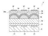
- FIG. 2 is a cross-sectional view showing the structure of the chemical sensor 3 according to the present embodiment.
- the chemical sensor 3 includes a photodiode 21 formed on the substrate 2, a protective insulating layer 31, a spectral layer 32, an on-chip lens 33, an antireflection layer 34 formed on the substrate 2, A planarization layer 35, a surface layer 36, and a probe material layer 37 are provided.
- a protective insulating layer 31 is laminated on the substrate 2, and a spectral layer 32 is laminated on the protective insulating layer 31.
- An on-chip lens 33 is formed on the spectral layer 32, and the on-chip lens 33 is covered with an antireflection layer 34.
- a planarizing layer 35 is laminated on the antireflection layer 34, and a surface layer 36 is laminated on the planarizing layer 35.
- a probe material layer 37 is laminated on the surface layer 36.
- the substrate 2 is made of, for example, single crystal silicon, and one main surface side of the substrate 2 is a light receiving surface, and a photodiode 21 made of an impurity region is formed on the surface layer on the light receiving surface side.
- the photodiodes 21 are two-dimensionally arranged as shown in FIG.
- the photodiode 21 may be provided only on one main surface side that is the light receiving surface side in the substrate 2 as illustrated, or may be provided from one main surface side to another main surface side.
- the chemical sensor 3 may have a CMOS (Complementary Metal Oxide Semiconductor) or CCD (Charge Coupled Device) type element structure, and element isolation or floating diffusion, not shown here, may be used as necessary. It is assumed that another impurity region is arranged.
- a gate insulating film, a gate electrode, etc. may be disposed on the substrate 2 provided with the impurity region including the photodiode 21.
- the protective insulating layer 31 is disposed so as to cover the gate insulating film and the gate electrode.
- the pixel circuit including the gate insulating film and the gate electrode may be disposed on the surface of the substrate 2 opposite to the light receiving surface.
- the protective insulating layer 31 is made of an insulating material and insulates the substrate 2 from the upper layer.
- the protective insulating layer 31 needs to transmit at least the fluorescence wavelength.
- the spectral layer 32 is made of a spectral material that attenuates the excitation light wavelength and transmits the fluorescence wavelength.
- the spectral layer 32 may be a color filter using such a pigment or dye, or may be a color filter using multilayer film interference.
- the spectral layer 32 may be provided at a different position, for example, between the planarization layer 35 and the surface layer 36.
- the on-chip lens 33 condenses incident fluorescence on the photodiode 21.
- the on-chip lens 33 is provided corresponding to each photodiode 21 and may have a hemispherical shape that is convex with respect to the light incident direction.
- One on-chip lens 33 may be provided for a plurality of photodiodes 21, but it is more efficient that one on-chip lens 33 corresponds to one photodiode 21. can do.
- the shape of the on-chip lens 33 is not limited to a hemispherical shape, and other lens shapes can be used.
- the refractive index of the on-chip lens 33 is defined as a refractive index n0.
- the on-chip lens 33 is preferably made of a material that is transparent at least in the fluorescence wavelength region to be detected, and a material having a large refractive index difference from the planarization layer 35 described later.
- the antireflection layer 34 is a layer for preventing reflection on the surface of the on-chip lens 33, and can be formed conformally along the on-chip lens 33.
- the antireflection layer 34 can be made of silicon nitride oxide or the like, and can have a multilayer structure as shown in the figure.
- the planarization layer 35 covers the on-chip lens 33 and forms a probe holding surface 35 a parallel to the substrate 2.
- the on-chip lens 33 is formed in a lens shape such as a hemispherical shape, but the planarization layer 35 forms a probe holding surface 35a for holding the probe material by embedding this shape.
- the planarizing layer 35 is made of a material having a refractive index that is sufficiently different from the refractive index n0 of the on-chip lens 33 so that the light condensing characteristic of the on-chip lens 33 to the photodiode 21 can be maintained.
- the refractive index of the planarization layer 35 is defined as a refractive index n1.
- the planarizing layer 35 is formed using a material having a small refractive index, and the refractive index n0 of the on-chip lens 33 and the refractive index n1 of the planarizing layer 35 are N1 ⁇ n0.
- the thickness of the planarizing layer 35 may be a thickness that can embed the lens shape of the on-chip lens 33.
- a material having a focal length as small as that obtained when the flattening layer 35 is replaced with air is selected and a refractive index difference
- the surface layer 36 is a layer to which the probe material is fixed. Since the on-chip lens 33 is flattened by the flattening layer 35, the surface layer 36 can be formed flat.
- the surface layer 36 can be made of diamond, silicon nitride, silicon oxide, or the like. Of these, diamond is used to form a strong bond between the probe material and the surface layer 36 by a surface treatment described later. It becomes possible.
- the surface layer 36 can be subjected to a surface treatment for improving adhesion with the probe material.
- the surface layer 36 is made of diamond, it can be aminated by ultraviolet irradiation in an ammonia gas atmosphere.
- the probe material is fixed to the surface layer 36, by introducing a carboxylic acid into the probe material, an amino bond is generated between the surface layer 36 and the probe material, and both are chemically fixed. Is possible.
- the surface layer 36 is made of silicon oxide, a functional group can be introduced by silane coupling treatment and bonded to the probe material.
- the surface treatment can be performed not only on the entire surface layer 36 but on an arbitrary region. By performing the surface treatment for each region facing the on-chip lens 33, it becomes possible to fix a probe material described later to the surface layer 36 for each on-chip lens 33.
- the chemical sensor 3 is provided to the user in this state, and the user can use an arbitrary probe material by fixing it to the probe holding surface 35a.
- the probe material layer 37 is made of a probe material (DNA (Deoxyribonucleic acid), RNA (ribonucleic acid), protein, or antigen) and is fixed to the probe holding surface 35a. As described above, the on-chip lens of the probe holding surface 35a. In the case where the surface treatment is applied to the region facing 33, the probe material layer 37 is formed only in the region subjected to the surface treatment, whereby one region of the probe material layer 37 is provided as one region. Corresponding to the on-chip lens 33 and the photodiode 21, it is possible to detect fluorescence with high accuracy.
- the distance between the probe material layer 37 and the photodiode 21 is preferably 10 ⁇ m or less. If the distance is longer than this, the light emitted from the probe material layer 37 is not sufficiently condensed on the photodiode 21, and the sensitivity and accuracy may be deteriorated.
- the chemical sensor 3 is configured as described above.
- the fluorescence generated from the probe material layer 37 is condensed on the photodiode 21 by the on-chip lens 33 and detected. Since the probe material layer 37 is laminated on the planarization layer 35 or the surface layer 36 formed immediately above, the distance from the probe material layer 37 to the photodiode 21 can be shortened, and the fluorescence is condensed. It is possible to improve the rate.
- a photodiode 21 made of an impurity region is formed on one main surface side of the substrate 2 made of single crystal silicon or the like by ion implantation from above the mask and heat treatment. Furthermore, another impurity region may be formed inside the substrate 2, and a gate insulating film and a gate electrode may be formed on the substrate.
- a protective insulating layer 31 is laminated on the substrate 2 on which the photodiode 21 is formed.
- the protective insulating layer 31 preferably has a thickness that allows the focal point of the on-chip lens 33 to be located in the photodiode 21 in consideration of the focal length of the on-chip lens 33 to be formed later.
- the spectral layer 32 is laminated on the protective insulating layer 31.
- the spectral layer 32 can be laminated by spin coating or the like.
- the on-chip lens 33 is formed on the spectral layer 32.
- the on-chip lens 33 can be formed by forming a film made of a constituent material of the on-chip lens 33 (hereinafter, a material film) and molding the film.
- an island-shaped resist pattern corresponding to each photodiode 21 is formed on the material film. Thereafter, the resist pattern is flowed by a melt flow method, and is molded into a convex lens shape by surface tension.
- the curved shape of the resist pattern can be transferred to the material film by etching the material film together with the resist pattern from above the resist pattern having a convex lens shape.
- the convex on-chip lens 33 can be formed on each photodiode 21.
- An antireflection layer 34 can be laminated on the on-chip lens 33 as necessary.
- a planarizing layer 35 is laminated on the on-chip lens 33 (or the antireflection layer 34).
- the planarizing layer 35 can be stacked by a spin coat method or the like.
- material solution when the solution of the constituent material of the planarization layer 35 (hereinafter, “material solution”) has a low viscosity, there is a limit to the coating thickness of the solution by spin coating on the on-chip lens 33.
- the material solution is applied by embedding the lens shape of the on-chip lens 33, there is no need to increase the coating film thickness. For example, a coating film of about 1 ⁇ m from the top of the on-chip lens 33.
- the material solution can be applied in thickness.
- the material solution has a low viscosity, the embedding property of the on-chip lens 33 is good, and it is possible to provide a good image quality with few image quality defects due to voids.
- the material solution is cured by heat treatment or the like, and the planarization layer 35 can be formed.
- a surface layer 36 is laminated on the planarizing layer 35 as necessary.
- the surface layer 36 can be formed by a CVD (Chemical Vapor Deposition) method or the like.
- the surface layer 36 can be subjected to a surface treatment that improves the bonding property with the probe material as described above. This surface treatment can be formed only in a region facing the on-chip lens 33.
- a probe material layer 37 is laminated on the surface layer 36 or the planarization layer 35.
- the probe material layer 37 can be formed by dropping the probe material onto the surface layer 36 or the planarizing layer 35 and bonding them.
- the probe material layer 37 can be laminated only on the region where the surface treatment is applied.
- the chemical sensor 3 can be manufactured as described above.
- 5'-fluoresceinized DNA can be used. If DNA having a complementary sequence is contained in the sample with respect to this 5′-fluoresceinized DNA, a hybridization reaction occurs, and the probe material is obtained from single-stranded DNA (ss-DNA). , Double-stranded DNA (ds-DNA).
- the photodiode 21 detects that the emission wavelength and intensity of the fluorescence change due to the change in the dielectric constant around the fluorescent molecule due to this change.
- the probe material when DNA is used as the probe material, the probe material is exemplified by using DNA that is not fluorescently labeled and using 5′-fluoresceinized DNA on the sample side.
- DNA having a sequence complementary to DNA as a probe material is contained in the sample, a hybridization reaction occurs and ds-DNA having a fluorescent label is obtained. Fluorescence emission from the fluorescent label is detected by the photodiode 21.
- DNA that is not fluorescently labeled is used as the probe material, and no fluorescent dye is introduced into the sample side.
- DNA having a sequence complementary to DNA as a probe material is contained in the sample, a hybridization reaction occurs and ds-DNA is obtained.
- the fluorescent labeling is introduced into the ds-DNA part by selectively staining only the ds-DNA and performing the fluorescent labeling using, for example, a PicoGreen double-stranded DNA quantitative reagent manufactured by Molecular probe. Fluorescence emission from the fluorescent label is detected by the photodiode 21.
- Fluorescence generated in the probe material layer 37 as described above and resulting from the combination of the target material and the probe material passes through the surface layer 36 and the planarization layer 35 and enters the on-chip lens 33. At this time, the reflection of fluorescence is prevented by the antireflection layer 34 formed on the surface of the on-chip lens 33.
- the fluorescence incident on the on-chip lens 33 is collected by the on-chip lens 33, the excitation light is removed by the spectral layer 32, passes through the protective insulating layer 31, and reaches the photodiode 21.
- the intensity of the fluorescence reaching the photodiode 21 can be improved, and crosstalk between adjacent photodiodes 21 can be prevented.
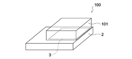
- FIG. 3 is a schematic diagram showing the chemical sensor module 100. As shown in the figure, the chemical sensor module 100 is configured by integrally connecting an excitation light source 101 to the chemical sensor 3. In FIG. 3, the excitation light source 101 is shown in close contact with the chemical sensor 3, but this is not always necessary, and there is a certain distance between the chemical sensor 3 and the excitation light source 101. Also good.
- a biomolecule detection apparatus according to a second embodiment of the present technology will be described.
- the configuration of the chemical sensor is different from that of the biomolecule detection apparatus according to the first embodiment.
- the description of the same configuration as that of the biomolecule detection apparatus according to the first embodiment is omitted.
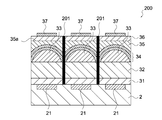
- FIG. 3 is a schematic diagram showing the structure of the chemical sensor 200 according to the present embodiment. As shown in the figure, the chemical sensor 3 includes a light shielding wall 201 in addition to the structure of the chemical sensor 3 according to the first embodiment.
- the light shielding wall 201 is a structure for preventing the crosstalk in which the fluorescence generated from the probe material layer 37 corresponding to the specific photodiode 21 is detected by the adjacent photodiode 21.
- the light shielding wall 201 can be formed between the on-chip lenses 33 from the planarization layer 35 to the protective insulating layer 31. Further, the light shielding wall 201 may be formed over a part of the layer structure such as the planarization layer 35 alone, the planarization layer 35, and the spectral layer 32.
- the light shielding wall 201 can be created as follows. That is, after the planarization layer 35 is provided, a photoresist is applied and patterned to remove a portion of the photoresist for forming the light shielding wall 201. Next, the planarizing layer 35 and the like are removed by a dry etching method, and the photoresist is also removed. Then, a negative black resist is applied, and only a portion where the light shielding wall 201 is formed is exposed. As a result, the light shielding wall 201 made of black resist can be embedded.
- the fluorescence generated from the probe material layer 37 corresponding to the specific photodiode 21 is shielded by the light shielding wall 201. Thereby, crosstalk between the photodiodes 21 can be prevented, and high detection accuracy can be obtained.
- the present technology is not limited to the above embodiments, and can be changed without departing from the gist of the present technology.
- [Chemical sensor A] A photodiode made of an impurity region is formed on one main surface side of the substrate made of single crystal silicon by ion implantation from above the mask and subsequent heat treatment, and another impurity region is formed inside the substrate. A gate insulating film and a gate electrode were formed on the substrate. Thereafter, a protective insulating layer was formed over the substrate. At this time, the protective insulating layer has a thickness adjusted so that the focal point of the on-chip lens is positioned in the photodiode in consideration of the focal length of the on-chip lens to be formed later.
- a spectral layer made of a red color filter (transmitting a wavelength of 550 nm or more) was formed on the protective insulating layer.
- a silicon nitride film was first formed on the spectral layer, and an island-shaped resist pattern corresponding to the photodiode to be written thereon was formed.
- the melt flow method was applied and heat treatment was performed to cause the resist pattern to flow, and the lens was shaped into a convex lens shape by surface tension. Thereafter, the silicon nitride film was etched together with the resist pattern from above the resist pattern having a convex lens shape, and the curved shape of the resist pattern was transferred to the silicon nitride film. Thus, a convex on-chip lens made of silicon nitride was formed on each photodiode.
- a planarizing layer was formed in a state where the lens shape of the on-chip lens was embedded.
- a transparent material having a sufficient refractive index difference with respect to silicon nitride constituting the on-chip lens was used.
- a planarization layer was formed by applying a spin coating method.
- the solvent in the solution applied on the on-chip lens was dried and removed by heat treatment at 120 ° C. for 1 minute, and then the fluorine-containing polysiloxane resin was sufficiently cured by heat treatment at 230 ° C. for 5 minutes. Thereby, the lens shape of the on-chip lens was embedded, and a flattened layer made of a fluorine-containing polysiloxane resin molded flat was formed.
- chemical sensor A a surface layer made of diamond was laminated by CVD using a mixed gas made of methane and hydrogen. Furthermore, the surface of the diamond was aminated by UV irradiation in an ammonia gas atmosphere. The distance between the photodiode of the chemical sensor thus fabricated and the surface layer surface was 7 ⁇ m.
- the chemical sensor produced in this way is designated as chemical sensor A.
- Chemical sensor B In the chemical sensor A, the surface layer was made of silicon oxide instead of diamond. Specifically, a silicon oxide was laminated on the planarizing layer by CVD. Further, the surface layer made of this silicon oxide was subjected to oxygen ashing treatment and treated with an amino silane coupling agent to aminate the surface. The chemical sensor produced in this way is designated as chemical sensor B.
- Chemical sensor E In the chemical sensor A, an on-chip lens was not formed, and a transparent resin (acrylic) was formed on the on-chip lens and the flattening layer so as to have the same film thickness as the on-chip lens and the flattening layer. .
- the chemical sensor produced in this manner is referred to as a chemical sensor E.
- Chemical sensor F In the chemical sensor B, an on-chip lens was not formed, and a transparent resin (acrylic) was formed on the on-chip lens and the flattening layer so as to have the same film thickness as the on-chip lens and the flattening layer. .
- the chemical sensor manufactured in this way is referred to as a chemical sensor F.
- the chemical sensor was treated with succinic acid to generate a carboxyl group on the surface, and then reacted with an oligonucleotide (DNA) aminated at the 5'-end.
- the oligonucleotide is 20mer, and its sequence is AAAATAAAATAAAAAATAAAT (buffer: PBS (Sodium phosphate: 10 mM; NaCl: 0.1M)).
- the buffer solution was dropped on the chemical sensor and left at 50 ° C. for 1 hour.
- PBS-Tween Sodium phosphate: 10 mM; NaCl: 0.1 M; 0.65% (w / v) Tween 20
- an oligonucleotide having a 5'-terminal fluorescein was prepared as sample DNA.
- the prepared oligonucleotide sequences are TTTTATTTTTATTTTTTTA (sequence 1) which is complementary to the above sequence and CCCCGCCCCCCCCCGCCCCG (sequence 2) which is not complementary.
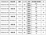
- the intensity of fluorescence from the washed chemical sensor was measured by excitation with light having a wavelength of 490 nm. Due to the characteristics of the color filter of the sensor, the intensity of the component having a wavelength of 550 nm or more in the fluorescence emitted from Fluorescein was measured. The measured intensity is shown in FIG. In the table, “ratio” is the intensity ratio between the array 1 and the array 2, and the larger the ratio, the lower the false detection rate.
- this technique can also take the following structures.
- a chemical sensor comprising: a flattening layer that covers and flattens the on-chip lens and forms a probe holding surface for holding a probe material.
- the incident light is fluorescence resulting from the binding between the probe material and the target material.
- a chemical sensor further comprising: a spectral layer made of a spectral material, which is laminated between the substrate and the on-chip lens or between the on-chip lens and the probe holding surface.
- a chemical sensor further comprising: a surface layer laminated on the planarizing layer to which the probe material is fixed.
- the chemical sensor according to any one of (1) to (4) above is made of diamond, and has been subjected to a surface treatment by ultraviolet irradiation in an ammonia gas atmosphere.
- planarizing layer is made of a material having a refractive index difference of 0.4 or more with respect to the on-chip lens.
- a chemical sensor module comprising: an excitation light source that is integrally attached to the chemical sensor and irradiates the chemical sensor with excitation light.
- a chemical sensor having a planarization layer forming a probe holding surface for holding A biomolecule detection apparatus comprising: a signal processing circuit connected to the chemical sensor and processing an output signal of the photodiode.
- Preparing a chemical sensor having a planarizing layer that forms a probe holding surface for holding A probe material layer is formed by laminating a probe material on the planarization layer, The measurement target substance is brought into contact with the probe material layer, and the target material amount contained in the measurement target substance is combined with the probe material, Remove the target substance that did not bind to the probe material, Irradiate the chemical sensor with excitation light, A biomolecule detection method in which fluorescence resulting from the binding between the target material and the probe material is detected by the photodiode.
Landscapes
- Health & Medical Sciences (AREA)
- Life Sciences & Earth Sciences (AREA)
- Immunology (AREA)
- Chemical & Material Sciences (AREA)
- Engineering & Computer Science (AREA)
- Molecular Biology (AREA)
- Biomedical Technology (AREA)
- Hematology (AREA)
- Urology & Nephrology (AREA)
- Physics & Mathematics (AREA)
- Analytical Chemistry (AREA)
- Biochemistry (AREA)
- General Health & Medical Sciences (AREA)
- General Physics & Mathematics (AREA)
- Pathology (AREA)
- Biotechnology (AREA)
- Microbiology (AREA)
- Cell Biology (AREA)
- Food Science & Technology (AREA)
- Medicinal Chemistry (AREA)
- Organic Chemistry (AREA)
- Zoology (AREA)
- Proteomics, Peptides & Aminoacids (AREA)
- Wood Science & Technology (AREA)
- Nuclear Medicine, Radiotherapy & Molecular Imaging (AREA)
- Biophysics (AREA)
- Bioinformatics & Cheminformatics (AREA)
- General Engineering & Computer Science (AREA)
- Genetics & Genomics (AREA)
- Investigating, Analyzing Materials By Fluorescence Or Luminescence (AREA)
- Solid State Image Pick-Up Elements (AREA)
Abstract
Description
上記基板は、平面状に配列する複数のフォトダイオードが形成されている。
上記オンチップレンズは、上記基板上に設けられた、入射光を上記フォトダイオードに集光する。
上記平坦化層は、上記オンチップレンズを被覆して平坦化し、プローブ材料を保持するためのプローブ保持面を形成する。
上記ケミカルセンサは、平面状に配列する複数のフォトダイオードが形成された基板と、上記基板上に設けられた入射光を上記フォトダイオードに集光するオンチップレンズと、上記オンチップレンズを被覆して平坦化しプローブ材料を保持するためのプローブ保持面を形成する平坦化層とを有する。
上記励起光源は、上記ケミカルセンサに一体的に装着され、上記ケミカルセンサに励起光を照射する。
上記ケミカルセンサは、平面状に配列する複数のフォトダイオードが形成された基板と、上記基板上に設けられた入射光を上記フォトダイオードに集光するオンチップレンズと、上記オンチップレンズを被覆して平坦化しプローブ材料を保持するためのプローブ保持面を形成する平坦化層とを有する。
上記信号処理回路は、上記ケミカルセンサに接続され、上記フォトダイオードの出力信号を処理する。
プローブ材料を上記平坦化層に積層させてプローブ材料層を形成する。
測定対象物質を上記プローブ材料層に接触させて、上記測定対象物質に含まれたターゲット材量を上記プローブ材料と結合させる。
上記プローブ材料と結合しなかった測定対象物質を除去する。
上記ケミカルセンサに励起光を照射する。
上記ターゲット材料と上記プローブ材料の結合に起因する蛍光を上記フォトダイオードによって検出する。
本技術の第1の実施形態に係る生体分子検出装置について説明する。
図1は、本実施形態に係る生体分子検出装置1の構成を示す模式図である。同図に示すように、生体分子検出装置1は、基板2上に設けられたケミカルセンサ3と、ケミカルセンサ3を駆動するための周辺回路から構成されている。詳細は後述するが、ケミカルセンサ3は、基板2上に配列された複数のフォトダイオード21を有する。
上記ケミカルセンサ3の構造について説明する。
上記ケミカルセンサ3の作製方法について説明する。
上述したケミカルセンサ3を用いた生体分子検出方法について説明する。
上記ケミカルセンサ3は、ケミカルセンサ3に励起光を照射する励起光源とモジュール化をすることが可能である。図3は、ケミカルセンサモジュール100を示す模式図である。同図に示すように、ケミカルセンサモジュール100は、ケミカルセンサ3に励起光源101が一体的に接続されて構成されている。なお、図3においては、ケミカルセンサ3に励起光源101が密着している形で記載しているが、必ずしも、その必要はなく、ケミカルセンサ3と励起光源101の間にある程度の距離があってもよい。
本技術の第2の実施形態に係る生体分子検出装置について説明する。本実施形態に係る生体分子検出装置においては、ケミカルセンサの構成が第1の実施形態に係る生体分子検出装置と異なる。以下、本実施形態において、第1の実施形態に係る生体分子検出装置と同一の構成については説明を省略する。
本実施形態に係る生体分子検出装置のケミカルセンサの構造について説明する。図3は本実施形態に係るケミカルセンサ200の構造を示す模式図である。同図に示すように、ケミカルセンサ3は、第1の実施形態に係るケミカルセンサ3の構造に加え、遮光壁201を有する。
単結晶シリコンからなる基板の一主面側に、マスク上からのイオン注入とその後の熱処理によって不純物領域からなるフォトダイオードを形成し、更に、基板の内部に他の不純物領域を形成し、さらに該基板上にゲート絶縁膜およびゲート電極を形成した。その後、基板上に保護絶縁層を成膜した。この際、保護絶縁層は、以降に形成するオンチップレンズの焦点距離を考慮し、オンチップレンズの焦点がフォトダイオード内に位置するように調整された膜厚とした。
上記ケミカルセンサAにおいて、表面層をダイヤモンドに替えてケイ素酸化物からなるものとした。具体的には、平坦化層上に、CVDによりケイ素酸化物を積層した。更に、このケイ素酸化物からなる表面層の酸素アッシング処理し、アミノ系シランカップリング剤にて処理を行い、表面をアミノ化した。このようにして作製したケミカルセンサをケミカルセンサBとする。
上記ケミカルセンサAにおいて、平坦化層を形成する際、スピンコートの膜厚を変え、更に、平坦化層の塗布を4回行うことで平坦化層の膜厚を厚くし、フォトダイオードと表面層表面の間の距離を11μmとした。このようにして作製したケミカルセンサをケミカルセンサCとする。
上記ケミカルセンサBにおいて、平坦化層を形成する際、スピンコートの膜厚を変え、更に、平坦化層の塗布を4回行うことで平坦化層の膜厚を厚くし、フォトダイオードと表面層表面の間の距離を11μmとした。このようにして作製したケミカルセンサをケミカルセンサDとする。
上記ケミカルセンサAにおいて、オンチップレンズを形成せず、オンチップレンズ及び平坦化層の部分に、透明樹脂(アクリル系)をオンチップレンズ及び平坦化層の膜厚と同じになるように形成した。このようにして作製したケミカルセンサをケミカルセンサEとする。
上記ケミカルセンサBにおいて、オンチップレンズを形成せず、オンチップレンズ及び平坦化層の部分に、透明樹脂(アクリル系)をオンチップレンズ及び平坦化層の膜厚と同じになるように形成した。このようにして作製したケミカルセンサをケミカルセンサFとする。
上記ケミカルセンサAにおいて、平坦化層を形成する際、スピンコートの膜厚を変え、更に、平坦化層の塗布を4回行うことで平坦化層の膜厚を厚くし、フォトダイオードと表面層表面の間の距離を10μmとした。このようにして作製したケミカルセンサをケミカルセンサGとする。
上記ケミカルセンサBにおいて、平坦化層を形成する際、スピンコートの膜厚を変え、更に、平坦化層の塗布を4回行うことで平坦化層の膜厚を厚くし、フォトダイオードと表面層表面の間の距離を10μmとした。このようにして作製したケミカルセンサをケミカルセンサHとする。
上記のようにしてそれぞれ作製したケミカルセンサA~Hについて、次のようにして蛍光強度測定を実施した。
サンプルDNAを充分な信頼性を持って検出するためには、今回用いた計測システムでは、強度として、約200以上の輝度を必要とする。図4より明らかなように、ケミカルセンサのフォトダイオードと表面層の表面の距離が10μmを超えると、充分な強度を得ることができなくなる。又、オンチップレンズを除いても同様で、充分な強度を得ることができなくなってしまう。さらに、配列1と配列2での強度比を見ると、表面層がダイヤモンドである場合の方がケイ素酸化物の場合よりも値が大きくなることが分かる。即ち、表面層の材質としてダイヤモンドを用いることにより、誤検出の少ないより精度のよい検出が可能となる。
平面状に配列する複数のフォトダイオードが形成された基板と、
上記基板上に設けられた、入射光を上記フォトダイオードに集光するオンチップレンズと、
上記オンチップレンズを被覆して平坦化し、プローブ材料を保持するためのプローブ保持面を形成する平坦化層と
を具備するケミカルセンサ。
上記(1)に記載のケミカルセンサであって、
前記入射光は、前記プローブ材料とターゲット材料の結合に起因する蛍光である
ケミカルセンサ。
上記(1)又は(2)に記載のケミカルセンサであって、
上記基板と上記オンチップレンズの間、又は上記オンチップレンズと上記プローブ保持面の間に積層された、分光材料からなる分光層
をさらに具備するケミカルセンサ。
上記(1)から(3)のうちいずれか一つに記載のケミカルセンサであって、
上記平坦化層に積層された、上記プローブ材料が固着する表面層
をさらに具備する
ケミカルセンサ。
上記(1)から(4)のうちいずれか一つに記載のケミカルセンサであって、
上記表面層は、ダイヤモンドからなり、アンモニアガス雰囲気中での紫外線照射による表面処理が施されている
ケミカルセンサ。
上記(1)から(5)のうちいずれか一つに記載のケミカルセンサであって、
上記表面処理は、上記オンチップレンズのそれぞれに対向する領域に形成されている
ケミカルセンサ。
上記(1)から(6)のうちいずれか一つに記載のケミカルセンサであって
上記オンチップレンズは、上記フォトダイオードのそれぞれに対して一つずつ設けられ、入射光を上記フォトダイオードのそれぞれに集光する
ケミカルセンサ。
上記(1)から(7)のうちいずれか一つに記載のケミカルセンサであって
上記オンチップレンズのそれぞれの間に設けられた遮光壁
をさらに具備するケミカルセンサ。
上記(1)から(8)のうちいずれか一つに記載のケミカルセンサであって
上記平坦化層は、上記オンチップレンズとの屈折率差が0.4以上である材料からなる
ケミカルセンサ。
上記(1)から(9)のうちいずれか一つに記載のケミカルセンサであって
上記平坦化層に積層されたプローブ材料からなるプローブ材料層
をさらに具備するケミカルセンサ。
上記(1)から(10)のうちいずれか一つに記載のケミカルセンサであって
上記プローブ材料層と上記フォトダイオードの間の距離は10μm以下である
ケミカルセンサ。
上記(1)から(11)のうちいずれか一つに記載のケミカルセンサであって、
上記プローブ材料層は、上記オンチップレンズのそれぞれに対向するように、区画されている
ケミカルセンサ。
上記(1)から(12)のうちいずれか一つに記載のケミカルセンサであって、
上記プローブ材料は、DNA、RNA、タンパク質又は抗原である
ケミカルセンサ。
平面状に配列する複数のフォトダイオードが形成された基板と、上記基板上に設けられた入射光を上記フォトダイオードに集光するオンチップレンズと、上記オンチップレンズを被覆して平坦化しプローブ材料を保持するためのプローブ保持面を形成する平坦化層とを有するケミカルセンサと、
上記ケミカルセンサに一体的に装着され、上記ケミカルセンサに励起光を照射する励起光源と
を具備するケミカルセンサモジュール。
平面状に配列する複数のフォトダイオードが形成された基板と、上記基板上に設けられた入射光を上記フォトダイオードに集光するオンチップレンズと、上記オンチップレンズを被覆して平坦化しプローブ材料を保持するためのプローブ保持面を形成する平坦化層とを有するケミカルセンサと、
上記ケミカルセンサに接続され、上記フォトダイオードの出力信号を処理する信号処理回路と
を具備する生体分子検出装置。
平面状に配列する複数のフォトダイオードが形成された基板と、上記基板上に設けられた入射光を上記フォトダイオードに集光するオンチップレンズと、上記オンチップレンズを被覆して平坦化しプローブ材料を保持するためのプローブ保持面を形成する平坦化層とを有するケミカルセンサを準備し、
プローブ材料を上記平坦化層に積層させてプローブ材料層を形成し、
測定対象物質を上記プローブ材料層に接触させて、上記測定対象物質に含まれたターゲット材量を上記プローブ材料と結合させ、
上記プローブ材料と結合しなかった測定対象物質を除去し、
上記ケミカルセンサに励起光を照射し、
上記ターゲット材料と上記プローブ材料の結合に起因する蛍光を上記フォトダイオードによって検出する
生体分子検出方法。
上記(16)に記載の生体分子検出方法であって、
上記蛍光を検出するステップでは、予め蛍光標識されている上記プローブ材料と上記ターゲット材料の相互作用による蛍光の波長及び輝度の変化を上記フォトダイオードによって検出する
生体分子検出方法。
上記(16)又は(17)に記載の生体分子検出方法であって、
上記蛍光を検出するステップでは、上記プローブ材料と結合した予め蛍光標識されているターゲット材料による蛍光を上記フォトダイオードによって検出する
生体分子検出方法。
上記(16)から(18)のうちいずれか一つに記載のケミカルセンサであって、
上記蛍光を検出するステップでは、上記プローブ材料と上記ターゲット材料の結合体に対して蛍光標識を実施し、その蛍光を上記フォトダイオードによって検出する
生体分子検出方法。
2…基板
3…ケミカルセンサ
21…フォトダイオード
31…保護絶縁層
32…分光層
33…オンチップレンズ
34…反射防止層
35…平坦化層
35a…プローブ保持面
36…表面層
37…プローブ材料層
100…ケミカルセンサモジュール
101…励起光源
200…ケミカルセンサ
201…遮光壁
Claims (19)
- 平面状に配列する複数のフォトダイオードが形成された基板と、
前記基板上に設けられた、入射光を前記フォトダイオードに集光するオンチップレンズと、
前記オンチップレンズを被覆して平坦化し、プローブ材料を保持するためのプローブ保持面を形成する平坦化層と
を具備するケミカルセンサ。 - 請求項1に記載のケミカルセンサであって、
前記入射光は、前記プローブ材料とターゲット材料の結合に起因する蛍光である
ケミカルセンサ。 - 請求項1に記載のケミカルセンサであって、
前記基板と前記オンチップレンズの間、又は前記オンチップレンズと前記プローブ保持面の間に積層された分光材料からなる分光層
をさらに具備するケミカルセンサ。 - 請求項1に記載のケミカルセンサであって、
前記平坦化層に積層された、前記プローブ材料が固着する表面層
をさらに具備する
ケミカルセンサ。 - 請求項4に記載のケミカルセンサであって、
前記表面層は、ダイヤモンドからなり、アンモニアガス雰囲気中での紫外線照射による表面処理が施されている
ケミカルセンサ。 - 請求項5に記載のケミカルセンサであって、
前記表面処理は、前記オンチップレンズのそれぞれに対向する領域に形成されている
ケミカルセンサ。 - 請求項1に記載のケミカルセンサであって、
前記オンチップレンズは、前記フォトダイオードのそれぞれに対して一つずつ設けられ、入射光を前記フォトダイオードのそれぞれに集光する
ケミカルセンサ。 - 請求項1に記載のケミカルセンサであって、
前記オンチップレンズのそれぞれの間に設けられた遮光壁
をさらに具備するケミカルセンサ。 - 請求項1に記載のケミカルセンサであって、
前記平坦化層は、前記オンチップレンズとの屈折率差が0.4以上である材料からなる
ケミカルセンサ。 - 請求項1に記載のケミカルセンサであって、
前記平坦化層に積層されたプローブ材料からなるプローブ材料層
をさらに具備するケミカルセンサ。 - 請求項10に記載のケミカルセンサであって、
前記プローブ材料層と前記フォトダイオードの間の距離は10μm以下である
ケミカルセンサ。 - 請求項10に記載のケミカルセンサであって、
前記プローブ材料層は、前記オンチップレンズのそれぞれに対向するように、区画されている
ケミカルセンサ。 - 請求項1に記載のケミカルセンサであって、
前記プローブ材料は、DNA、RNA、タンパク質又は抗原である
ケミカルセンサ。 - 平面状に配列する複数のフォトダイオードが形成された基板と、前記基板上に設けられた入射光を前記フォトダイオードに集光するオンチップレンズと、前記オンチップレンズを被覆して平坦化しプローブ材料を保持するためのプローブ保持面を形成する平坦化層とを有するケミカルセンサと、
前記ケミカルセンサに一体的に装着され、前記ケミカルセンサに励起光を照射する励起光源と
を具備するケミカルセンサモジュール。 - 平面状に配列する複数のフォトダイオードが形成された基板と、前記基板上に設けられた入射光を前記フォトダイオードに集光するオンチップレンズと、前記オンチップレンズを被覆して平坦化しプローブ材料を保持するためのプローブ保持面を形成する平坦化層とを有するケミカルセンサと、
前記ケミカルセンサに接続され、前記フォトダイオードの出力信号を処理する信号処理回路と
を具備する生体分子検出装置。 - 平面状に配列する複数のフォトダイオードが形成された基板と、前記基板上に設けられた入射光を前記フォトダイオードに集光するオンチップレンズと、前記オンチップレンズを被覆して平坦化しプローブ材料を保持するためのプローブ保持面を形成する平坦化層とを有するケミカルセンサを準備し、
プローブ材料を前記平坦化層に積層させてプローブ材料層を形成し、
測定対象物質を前記プローブ材料層に接触させて、前記測定対象物質に含まれたターゲット材量を前記プローブ材料と結合させ、
前記プローブ材料と結合しなかった測定対象物質を除去し、
前記ケミカルセンサに励起光を照射し、
前記ターゲット材料と前記プローブ材料の結合に起因する蛍光を前記フォトダイオードによって検出する
生体分子検出方法。 - 請求項16に記載の生体分子検出方法であって、
前記蛍光を検出するステップでは、予め蛍光標識されている前記プローブ材料と前記ターゲット材料の相互作用による蛍光の波長及び輝度の変化を前記フォトダイオードによって検出する
生体分子検出方法。 - 請求項16に記載の生体分子検出方法であって、
前記蛍光を検出するステップでは、前記プローブ材料と結合した予め蛍光標識されているターゲット材料による蛍光を前記フォトダイオードによって検出する
生体分子検出方法。 - 請求項16に記載の生体分子検出方法であって、
前記蛍光を検出するステップでは、前記プローブ材料と前記ターゲット材料の結合体に対して蛍光標識を実施し、その蛍光を前記フォトダイオードによって検出する
生体分子検出方法。
Priority Applications (4)
| Application Number | Priority Date | Filing Date | Title |
|---|---|---|---|
| KR1020147009129A KR102023216B1 (ko) | 2011-10-21 | 2012-10-11 | 케미컬 센서, 케미컬 센서 모듈, 생체분자 검출 장치 및 생체분자 검출 방법 |
| CN201280050546.7A CN103857997A (zh) | 2011-10-21 | 2012-10-11 | 化学传感器、化学传感器模块、生物分子检测装置及生物分子检测方法 |
| EP12842402.5A EP2770320B1 (en) | 2011-10-21 | 2012-10-11 | Chemical sensor, chemical sensor module, biomolecule detection device and biomolecule detection method |
| US14/348,988 US9670532B2 (en) | 2011-10-21 | 2012-10-11 | Chemical sensor, chemical sensor module, biomolecule detection apparatus, and biomolecule detection method |
Applications Claiming Priority (2)
| Application Number | Priority Date | Filing Date | Title |
|---|---|---|---|
| JP2011231470A JP2013088378A (ja) | 2011-10-21 | 2011-10-21 | ケミカルセンサ、ケミカルセンサモジュール、生体分子検出装置及び生体分子検出方法 |
| JP2011-231470 | 2011-10-21 |
Publications (1)
| Publication Number | Publication Date |
|---|---|
| WO2013057905A1 true WO2013057905A1 (ja) | 2013-04-25 |
Family
ID=48140574
Family Applications (1)
| Application Number | Title | Priority Date | Filing Date |
|---|---|---|---|
| PCT/JP2012/006509 Ceased WO2013057905A1 (ja) | 2011-10-21 | 2012-10-11 | ケミカルセンサ、ケミカルセンサモジュール、生体分子検出装置及び生体分子検出方法 |
Country Status (7)
| Country | Link |
|---|---|
| US (1) | US9670532B2 (ja) |
| EP (1) | EP2770320B1 (ja) |
| JP (1) | JP2013088378A (ja) |
| KR (1) | KR102023216B1 (ja) |
| CN (1) | CN103857997A (ja) |
| TW (1) | TWI503533B (ja) |
| WO (1) | WO2013057905A1 (ja) |
Cited By (1)
| Publication number | Priority date | Publication date | Assignee | Title |
|---|---|---|---|---|
| WO2021166689A1 (ja) * | 2020-02-18 | 2021-08-26 | ソニーセミコンダクタソリューションズ株式会社 | 受光装置、受光装置の製造方法、および、測距モジュール |
Families Citing this family (18)
| Publication number | Priority date | Publication date | Assignee | Title |
|---|---|---|---|---|
| SG11201707511UA (en) * | 2015-04-22 | 2017-10-30 | Shenzhen Genorivision Tech Co Ltd | A biosensor |
| WO2017045108A1 (en) | 2015-09-14 | 2017-03-23 | Shenzhen Genorivision Technology Co. Ltd. | A phototube and method of making it |
| WO2017045107A1 (en) * | 2015-09-14 | 2017-03-23 | Shenzhen Genorivision Technology Co. Ltd. | Biosensor |
| US11454591B2 (en) | 2015-12-07 | 2022-09-27 | Shenzhen Genorivision Technology Co., Ltd. | Biosensor |
| EP3472592A4 (en) * | 2016-06-21 | 2020-01-15 | Shenzhen Genorivision Technology Co., Ltd. | BIOSENSOR |
| ES2948117T3 (es) * | 2016-11-03 | 2023-08-31 | Mgi Tech Co Ltd | Biosensor |
| CN107084964B (zh) * | 2017-06-05 | 2021-02-05 | 京东方科技集团股份有限公司 | 生物传感器及其制备方法和进行生物传感的方法 |
| CN111295733B (zh) | 2017-09-19 | 2024-01-05 | 深圳华大智造科技股份有限公司 | 晶片级测序流通池制造 |
| TW201931615A (zh) * | 2017-12-06 | 2019-08-01 | 日商凸版印刷股份有限公司 | 固態攝影元件及其製造方法 |
| JP2020085666A (ja) * | 2018-11-26 | 2020-06-04 | ソニーセミコンダクタソリューションズ株式会社 | 生体由来物質検出用チップ、生体由来物質検出装置及び生体由来物質検出システム |
| JPWO2021014849A1 (ja) | 2019-07-24 | 2021-01-28 | ||
| US10957731B1 (en) * | 2019-10-04 | 2021-03-23 | Visera Technologies Company Limited | Sensor device and method for manufacturing the same |
| US11705472B2 (en) | 2019-10-10 | 2023-07-18 | Visera Technologies Company Limited | Biosensor and method of distinguishing a light |
| US11105745B2 (en) * | 2019-10-10 | 2021-08-31 | Visera Technologies Company Limited | Biosensor |
| US11630062B2 (en) * | 2019-10-10 | 2023-04-18 | Visera Technologies Company Limited | Biosensor and method of forming the same |
| CN115135988A (zh) * | 2020-02-19 | 2022-09-30 | 索尼半导体解决方案公司 | 生物体导出材料检测芯片、生物体导出材料检测装置及生物体导出材料检测系统 |
| US11557625B2 (en) * | 2020-04-20 | 2023-01-17 | Omnivision Technologies, Inc. | Image sensors with embedded wells for accommodating light emitters |
| JP7610464B2 (ja) * | 2021-04-28 | 2025-01-08 | 株式会社ジャパンディスプレイ | 検出装置 |
Citations (2)
| Publication number | Priority date | Publication date | Assignee | Title |
|---|---|---|---|---|
| JP2002202303A (ja) | 2000-12-27 | 2002-07-19 | Nikon Corp | 有機分子検出用半導体素子、有機分子検出用半導体装置及びこれを用いた有機分子の測定方法 |
| JP2006004991A (ja) | 2004-06-15 | 2006-01-05 | Casio Comput Co Ltd | 撮像装置及び生体高分子分析チップ |
Family Cites Families (14)
| Publication number | Priority date | Publication date | Assignee | Title |
|---|---|---|---|---|
| JPH11502617A (ja) * | 1995-03-10 | 1999-03-02 | メソ スケール テクノロジーズ,エルエルシー | 多重アレイの多重特異的な電気化学発光試験 |
| US6221687B1 (en) * | 1999-12-23 | 2001-04-24 | Tower Semiconductor Ltd. | Color image sensor with embedded microlens array |
| JP2001358320A (ja) | 2000-06-15 | 2001-12-26 | Sony Corp | 固体撮像素子及びその製造方法、並びにオンチップレンズ金型の製造方法 |
| US7078172B1 (en) * | 2000-08-08 | 2006-07-18 | Toyo Kohan Co., Ltd. | Substrate activation kit and method for detecting DNA and the like using the same |
| US20030035755A1 (en) * | 2001-08-16 | 2003-02-20 | Shu-Hui Chen | Organic electroluminescence (OEL)-based biochips |
| US6841663B2 (en) * | 2001-10-18 | 2005-01-11 | Agilent Technologies, Inc. | Chemical arrays |
| JP3657591B2 (ja) * | 2003-03-25 | 2005-06-08 | 独立行政法人科学技術振興機構 | pチャンネル電界効果トランジスタ及びそれを用いたセンサ |
| US6953925B2 (en) * | 2003-04-28 | 2005-10-11 | Stmicroelectronics, Inc. | Microlens integration |
| US20050233337A1 (en) * | 2004-04-19 | 2005-10-20 | Peck Bill J | Chemical arrays and methods of producing the same |
| EP1614460A1 (en) | 2004-07-08 | 2006-01-11 | Yamatake Corporation | Substrate for biochips |
| JP2007053183A (ja) * | 2005-08-17 | 2007-03-01 | Fujifilm Corp | 固体撮像素子 |
| KR100720535B1 (ko) * | 2005-10-11 | 2007-05-22 | 동부일렉트로닉스 주식회사 | 씨모스 이미지 센서 및 그 제조방법 |
| TWI346777B (en) * | 2007-07-20 | 2011-08-11 | Long Sun Huang | Micro-sensor for sensing chemical substance |
| EP2221606A3 (en) * | 2009-02-11 | 2012-06-06 | Samsung Electronics Co., Ltd. | Integrated bio-chip and method of fabricating the integrated bio-chip |
-
2011
- 2011-10-21 JP JP2011231470A patent/JP2013088378A/ja not_active Abandoned
-
2012
- 2012-09-24 TW TW101134980A patent/TWI503533B/zh not_active IP Right Cessation
- 2012-10-11 CN CN201280050546.7A patent/CN103857997A/zh active Pending
- 2012-10-11 WO PCT/JP2012/006509 patent/WO2013057905A1/ja not_active Ceased
- 2012-10-11 EP EP12842402.5A patent/EP2770320B1/en not_active Not-in-force
- 2012-10-11 US US14/348,988 patent/US9670532B2/en not_active Expired - Fee Related
- 2012-10-11 KR KR1020147009129A patent/KR102023216B1/ko not_active Expired - Fee Related
Patent Citations (2)
| Publication number | Priority date | Publication date | Assignee | Title |
|---|---|---|---|---|
| JP2002202303A (ja) | 2000-12-27 | 2002-07-19 | Nikon Corp | 有機分子検出用半導体素子、有機分子検出用半導体装置及びこれを用いた有機分子の測定方法 |
| JP2006004991A (ja) | 2004-06-15 | 2006-01-05 | Casio Comput Co Ltd | 撮像装置及び生体高分子分析チップ |
Non-Patent Citations (1)
| Title |
|---|
| See also references of EP2770320A4 |
Cited By (2)
| Publication number | Priority date | Publication date | Assignee | Title |
|---|---|---|---|---|
| WO2021166689A1 (ja) * | 2020-02-18 | 2021-08-26 | ソニーセミコンダクタソリューションズ株式会社 | 受光装置、受光装置の製造方法、および、測距モジュール |
| US12471399B2 (en) | 2020-02-18 | 2025-11-11 | Sony Semiconductor Solutions Corporation | Light receiving device, method for manufacturing light receiving device, and distance measuring module |
Also Published As
| Publication number | Publication date |
|---|---|
| JP2013088378A (ja) | 2013-05-13 |
| TWI503533B (zh) | 2015-10-11 |
| TW201321737A (zh) | 2013-06-01 |
| US20140295577A1 (en) | 2014-10-02 |
| EP2770320B1 (en) | 2017-08-09 |
| US9670532B2 (en) | 2017-06-06 |
| EP2770320A1 (en) | 2014-08-27 |
| EP2770320A4 (en) | 2015-03-18 |
| KR102023216B1 (ko) | 2019-11-04 |
| CN103857997A (zh) | 2014-06-11 |
| KR20140077904A (ko) | 2014-06-24 |
Similar Documents
| Publication | Publication Date | Title |
|---|---|---|
| KR102023216B1 (ko) | 케미컬 센서, 케미컬 센서 모듈, 생체분자 검출 장치 및 생체분자 검출 방법 | |
| JP7384967B2 (ja) | 生物学的又は化学的分析のためのバイオセンサ及びその製造方法 | |
| TWI521205B (zh) | Chemical detectors, biological molecular detection devices and biological molecular detection methods | |
| KR100822672B1 (ko) | 이미지센서를 이용한 진단장치 및 그 제조방법 | |
| AU775888B2 (en) | System and method for detecting molecules using an active pixel sensor | |
| JP6011544B2 (ja) | ケミカルセンサ、ケミカルセンサモジュール、化学物質検出装置及び化学物質検出方法 | |
| CN101769856A (zh) | 样品检测基板及制造方法、生物芯片、生物材料检测设备 | |
| CN103733341B (zh) | 图像传感器、其制造方法及检查装置 | |
| JP7065900B2 (ja) | センサ装置およびその製造方法 | |
| JP4741855B2 (ja) | 生体高分子分析チップ、分析支援装置及び生体高分子分析方法 | |
| US20170241997A1 (en) | Chemical sensor, method of producing chemical sensor, and chemical detection apparatus | |
| JP2004205335A (ja) | 光学的dnaセンサ、dna読取装置、dnaの同定方法及び光学的dnaセンサの製造方法 | |
| JP4802508B2 (ja) | 撮像装置、生体高分子分析チップ及び分析支援装置 | |
| JP3859050B2 (ja) | バイオチップ読み取り装置 | |
| JP2002350349A (ja) | 蛍光検出装置 | |
| JP4952313B2 (ja) | 蛍光検出装置及び生体高分子分析装置 | |
| JP2005351802A (ja) | 生体高分子分析チップ、生体高分子アレイフィルム、生体高分子チップの製造方法 |
Legal Events
| Date | Code | Title | Description |
|---|---|---|---|
| 121 | Ep: the epo has been informed by wipo that ep was designated in this application |
Ref document number: 12842402 Country of ref document: EP Kind code of ref document: A1 |
|
| WWE | Wipo information: entry into national phase |
Ref document number: 14348988 Country of ref document: US |
|
| ENP | Entry into the national phase |
Ref document number: 20147009129 Country of ref document: KR Kind code of ref document: A |
|
| REEP | Request for entry into the european phase |
Ref document number: 2012842402 Country of ref document: EP |
|
| WWE | Wipo information: entry into national phase |
Ref document number: 2012842402 Country of ref document: EP |
|
| NENP | Non-entry into the national phase |
Ref country code: DE |