WO2013065453A1 - 熱可塑性液晶ポリマーフィルムならびにこれを用いた積層体および回路基板 - Google Patents
熱可塑性液晶ポリマーフィルムならびにこれを用いた積層体および回路基板 Download PDFInfo
- Publication number
- WO2013065453A1 WO2013065453A1 PCT/JP2012/076086 JP2012076086W WO2013065453A1 WO 2013065453 A1 WO2013065453 A1 WO 2013065453A1 JP 2012076086 W JP2012076086 W JP 2012076086W WO 2013065453 A1 WO2013065453 A1 WO 2013065453A1
- Authority
- WO
- WIPO (PCT)
- Prior art keywords
- film
- liquid crystal
- crystal polymer
- heating
- thermoplastic liquid
- Prior art date
- Legal status (The legal status is an assumption and is not a legal conclusion. Google has not performed a legal analysis and makes no representation as to the accuracy of the status listed.)
- Ceased
Links
Images

Classifications
-
- H—ELECTRICITY
- H05—ELECTRIC TECHNIQUES NOT OTHERWISE PROVIDED FOR
- H05K—PRINTED CIRCUITS; CASINGS OR CONSTRUCTIONAL DETAILS OF ELECTRIC APPARATUS; MANUFACTURE OF ASSEMBLAGES OF ELECTRICAL COMPONENTS
- H05K1/00—Printed circuits
- H05K1/02—Details
- H05K1/03—Use of materials for the substrate
- H05K1/0313—Organic insulating material
-
- B—PERFORMING OPERATIONS; TRANSPORTING
- B32—LAYERED PRODUCTS
- B32B—LAYERED PRODUCTS, i.e. PRODUCTS BUILT-UP OF STRATA OF FLAT OR NON-FLAT, e.g. CELLULAR OR HONEYCOMB, FORM
- B32B15/00—Layered products comprising a layer of metal
- B32B15/04—Layered products comprising a layer of metal comprising metal as the main or only constituent of a layer, which is next to another layer of the same or of a different material
- B32B15/08—Layered products comprising a layer of metal comprising metal as the main or only constituent of a layer, which is next to another layer of the same or of a different material of synthetic resin
-
- B—PERFORMING OPERATIONS; TRANSPORTING
- B32—LAYERED PRODUCTS
- B32B—LAYERED PRODUCTS, i.e. PRODUCTS BUILT-UP OF STRATA OF FLAT OR NON-FLAT, e.g. CELLULAR OR HONEYCOMB, FORM
- B32B15/00—Layered products comprising a layer of metal
- B32B15/04—Layered products comprising a layer of metal comprising metal as the main or only constituent of a layer, which is next to another layer of the same or of a different material
- B32B15/08—Layered products comprising a layer of metal comprising metal as the main or only constituent of a layer, which is next to another layer of the same or of a different material of synthetic resin
- B32B15/09—Layered products comprising a layer of metal comprising metal as the main or only constituent of a layer, which is next to another layer of the same or of a different material of synthetic resin comprising polyesters
-
- B—PERFORMING OPERATIONS; TRANSPORTING
- B32—LAYERED PRODUCTS
- B32B—LAYERED PRODUCTS, i.e. PRODUCTS BUILT-UP OF STRATA OF FLAT OR NON-FLAT, e.g. CELLULAR OR HONEYCOMB, FORM
- B32B15/00—Layered products comprising a layer of metal
- B32B15/20—Layered products comprising a layer of metal comprising aluminium or copper
-
- B—PERFORMING OPERATIONS; TRANSPORTING
- B32—LAYERED PRODUCTS
- B32B—LAYERED PRODUCTS, i.e. PRODUCTS BUILT-UP OF STRATA OF FLAT OR NON-FLAT, e.g. CELLULAR OR HONEYCOMB, FORM
- B32B27/00—Layered products comprising a layer of synthetic resin
- B32B27/18—Layered products comprising a layer of synthetic resin characterised by the use of special additives
- B32B27/20—Layered products comprising a layer of synthetic resin characterised by the use of special additives using fillers, pigments, thixotroping agents
-
- B—PERFORMING OPERATIONS; TRANSPORTING
- B32—LAYERED PRODUCTS
- B32B—LAYERED PRODUCTS, i.e. PRODUCTS BUILT-UP OF STRATA OF FLAT OR NON-FLAT, e.g. CELLULAR OR HONEYCOMB, FORM
- B32B27/00—Layered products comprising a layer of synthetic resin
- B32B27/28—Layered products comprising a layer of synthetic resin comprising synthetic resins not wholly covered by any one of the sub-groups B32B27/30 - B32B27/42
- B32B27/286—Layered products comprising a layer of synthetic resin comprising synthetic resins not wholly covered by any one of the sub-groups B32B27/30 - B32B27/42 comprising polysulphones; polysulfides
-
- B—PERFORMING OPERATIONS; TRANSPORTING
- B32—LAYERED PRODUCTS
- B32B—LAYERED PRODUCTS, i.e. PRODUCTS BUILT-UP OF STRATA OF FLAT OR NON-FLAT, e.g. CELLULAR OR HONEYCOMB, FORM
- B32B27/00—Layered products comprising a layer of synthetic resin
- B32B27/32—Layered products comprising a layer of synthetic resin comprising polyolefins
-
- B—PERFORMING OPERATIONS; TRANSPORTING
- B32—LAYERED PRODUCTS
- B32B—LAYERED PRODUCTS, i.e. PRODUCTS BUILT-UP OF STRATA OF FLAT OR NON-FLAT, e.g. CELLULAR OR HONEYCOMB, FORM
- B32B27/00—Layered products comprising a layer of synthetic resin
- B32B27/32—Layered products comprising a layer of synthetic resin comprising polyolefins
- B32B27/322—Layered products comprising a layer of synthetic resin comprising polyolefins comprising halogenated polyolefins, e.g. PTFE
-
- B—PERFORMING OPERATIONS; TRANSPORTING
- B32—LAYERED PRODUCTS
- B32B—LAYERED PRODUCTS, i.e. PRODUCTS BUILT-UP OF STRATA OF FLAT OR NON-FLAT, e.g. CELLULAR OR HONEYCOMB, FORM
- B32B27/00—Layered products comprising a layer of synthetic resin
- B32B27/34—Layered products comprising a layer of synthetic resin comprising polyamides
-
- B—PERFORMING OPERATIONS; TRANSPORTING
- B32—LAYERED PRODUCTS
- B32B—LAYERED PRODUCTS, i.e. PRODUCTS BUILT-UP OF STRATA OF FLAT OR NON-FLAT, e.g. CELLULAR OR HONEYCOMB, FORM
- B32B27/00—Layered products comprising a layer of synthetic resin
- B32B27/36—Layered products comprising a layer of synthetic resin comprising polyesters
-
- B—PERFORMING OPERATIONS; TRANSPORTING
- B32—LAYERED PRODUCTS
- B32B—LAYERED PRODUCTS, i.e. PRODUCTS BUILT-UP OF STRATA OF FLAT OR NON-FLAT, e.g. CELLULAR OR HONEYCOMB, FORM
- B32B37/00—Methods or apparatus for laminating, e.g. by curing or by ultrasonic bonding
- B32B37/06—Methods or apparatus for laminating, e.g. by curing or by ultrasonic bonding characterised by the heating method
-
- B—PERFORMING OPERATIONS; TRANSPORTING
- B32—LAYERED PRODUCTS
- B32B—LAYERED PRODUCTS, i.e. PRODUCTS BUILT-UP OF STRATA OF FLAT OR NON-FLAT, e.g. CELLULAR OR HONEYCOMB, FORM
- B32B37/00—Methods or apparatus for laminating, e.g. by curing or by ultrasonic bonding
- B32B37/14—Methods or apparatus for laminating, e.g. by curing or by ultrasonic bonding characterised by the properties of the layers
- B32B37/16—Methods or apparatus for laminating, e.g. by curing or by ultrasonic bonding characterised by the properties of the layers with all layers existing as coherent layers before laminating
- B32B37/18—Methods or apparatus for laminating, e.g. by curing or by ultrasonic bonding characterised by the properties of the layers with all layers existing as coherent layers before laminating involving the assembly of discrete sheets or panels only
- B32B37/182—Methods or apparatus for laminating, e.g. by curing or by ultrasonic bonding characterised by the properties of the layers with all layers existing as coherent layers before laminating involving the assembly of discrete sheets or panels only one or more of the layers being plastic
-
- C—CHEMISTRY; METALLURGY
- C08—ORGANIC MACROMOLECULAR COMPOUNDS; THEIR PREPARATION OR CHEMICAL WORKING-UP; COMPOSITIONS BASED THEREON
- C08J—WORKING-UP; GENERAL PROCESSES OF COMPOUNDING; AFTER-TREATMENT NOT COVERED BY SUBCLASSES C08B, C08C, C08F, C08G or C08H
- C08J5/00—Manufacture of articles or shaped materials containing macromolecular substances
- C08J5/18—Manufacture of films or sheets
-
- C—CHEMISTRY; METALLURGY
- C09—DYES; PAINTS; POLISHES; NATURAL RESINS; ADHESIVES; COMPOSITIONS NOT OTHERWISE PROVIDED FOR; APPLICATIONS OF MATERIALS NOT OTHERWISE PROVIDED FOR
- C09K—MATERIALS FOR MISCELLANEOUS APPLICATIONS, NOT PROVIDED FOR ELSEWHERE
- C09K19/00—Liquid crystal materials
- C09K19/04—Liquid crystal materials characterised by the chemical structure of the liquid crystal components, e.g. by a specific unit
- C09K19/38—Polymers
- C09K19/3804—Polymers with mesogenic groups in the main chain
- C09K19/3809—Polyesters; Polyester derivatives, e.g. polyamides
-
- H—ELECTRICITY
- H05—ELECTRIC TECHNIQUES NOT OTHERWISE PROVIDED FOR
- H05K—PRINTED CIRCUITS; CASINGS OR CONSTRUCTIONAL DETAILS OF ELECTRIC APPARATUS; MANUFACTURE OF ASSEMBLAGES OF ELECTRICAL COMPONENTS
- H05K1/00—Printed circuits
- H05K1/02—Details
- H05K1/03—Use of materials for the substrate
- H05K1/0313—Organic insulating material
- H05K1/032—Organic insulating material consisting of one material
-
- H—ELECTRICITY
- H05—ELECTRIC TECHNIQUES NOT OTHERWISE PROVIDED FOR
- H05K—PRINTED CIRCUITS; CASINGS OR CONSTRUCTIONAL DETAILS OF ELECTRIC APPARATUS; MANUFACTURE OF ASSEMBLAGES OF ELECTRICAL COMPONENTS
- H05K1/00—Printed circuits
- H05K1/02—Details
- H05K1/03—Use of materials for the substrate
- H05K1/0313—Organic insulating material
- H05K1/032—Organic insulating material consisting of one material
- H05K1/0326—Organic insulating material consisting of one material containing O
-
- H—ELECTRICITY
- H05—ELECTRIC TECHNIQUES NOT OTHERWISE PROVIDED FOR
- H05K—PRINTED CIRCUITS; CASINGS OR CONSTRUCTIONAL DETAILS OF ELECTRIC APPARATUS; MANUFACTURE OF ASSEMBLAGES OF ELECTRICAL COMPONENTS
- H05K3/00—Apparatus or processes for manufacturing printed circuits
- H05K3/46—Manufacturing multilayer circuits
- H05K3/4611—Manufacturing multilayer circuits by laminating two or more circuit boards
- H05K3/4626—Manufacturing multilayer circuits by laminating two or more circuit boards characterised by the insulating layers or materials
-
- B—PERFORMING OPERATIONS; TRANSPORTING
- B32—LAYERED PRODUCTS
- B32B—LAYERED PRODUCTS, i.e. PRODUCTS BUILT-UP OF STRATA OF FLAT OR NON-FLAT, e.g. CELLULAR OR HONEYCOMB, FORM
- B32B2250/00—Layers arrangement
- B32B2250/42—Alternating layers, e.g. ABAB(C), AABBAABB(C)
-
- B—PERFORMING OPERATIONS; TRANSPORTING
- B32—LAYERED PRODUCTS
- B32B—LAYERED PRODUCTS, i.e. PRODUCTS BUILT-UP OF STRATA OF FLAT OR NON-FLAT, e.g. CELLULAR OR HONEYCOMB, FORM
- B32B2305/00—Condition, form or state of the layers or laminate
- B32B2305/55—Liquid crystals
-
- B—PERFORMING OPERATIONS; TRANSPORTING
- B32—LAYERED PRODUCTS
- B32B—LAYERED PRODUCTS, i.e. PRODUCTS BUILT-UP OF STRATA OF FLAT OR NON-FLAT, e.g. CELLULAR OR HONEYCOMB, FORM
- B32B2307/00—Properties of the layers or laminate
- B32B2307/20—Properties of the layers or laminate having particular electrical or magnetic properties, e.g. piezoelectric
- B32B2307/202—Conductive
-
- B—PERFORMING OPERATIONS; TRANSPORTING
- B32—LAYERED PRODUCTS
- B32B—LAYERED PRODUCTS, i.e. PRODUCTS BUILT-UP OF STRATA OF FLAT OR NON-FLAT, e.g. CELLULAR OR HONEYCOMB, FORM
- B32B2307/00—Properties of the layers or laminate
- B32B2307/50—Properties of the layers or laminate having particular mechanical properties
- B32B2307/538—Roughness
-
- B—PERFORMING OPERATIONS; TRANSPORTING
- B32—LAYERED PRODUCTS
- B32B—LAYERED PRODUCTS, i.e. PRODUCTS BUILT-UP OF STRATA OF FLAT OR NON-FLAT, e.g. CELLULAR OR HONEYCOMB, FORM
- B32B2309/00—Parameters for the laminating or treatment process; Apparatus details
- B32B2309/02—Temperature
-
- B—PERFORMING OPERATIONS; TRANSPORTING
- B32—LAYERED PRODUCTS
- B32B—LAYERED PRODUCTS, i.e. PRODUCTS BUILT-UP OF STRATA OF FLAT OR NON-FLAT, e.g. CELLULAR OR HONEYCOMB, FORM
- B32B2309/00—Parameters for the laminating or treatment process; Apparatus details
- B32B2309/08—Dimensions, e.g. volume
- B32B2309/10—Dimensions, e.g. volume linear, e.g. length, distance, width
- B32B2309/105—Thickness
-
- B—PERFORMING OPERATIONS; TRANSPORTING
- B32—LAYERED PRODUCTS
- B32B—LAYERED PRODUCTS, i.e. PRODUCTS BUILT-UP OF STRATA OF FLAT OR NON-FLAT, e.g. CELLULAR OR HONEYCOMB, FORM
- B32B2398/00—Unspecified macromolecular compounds
- B32B2398/20—Thermoplastics
-
- B—PERFORMING OPERATIONS; TRANSPORTING
- B32—LAYERED PRODUCTS
- B32B—LAYERED PRODUCTS, i.e. PRODUCTS BUILT-UP OF STRATA OF FLAT OR NON-FLAT, e.g. CELLULAR OR HONEYCOMB, FORM
- B32B2457/00—Electrical equipment
-
- B—PERFORMING OPERATIONS; TRANSPORTING
- B32—LAYERED PRODUCTS
- B32B—LAYERED PRODUCTS, i.e. PRODUCTS BUILT-UP OF STRATA OF FLAT OR NON-FLAT, e.g. CELLULAR OR HONEYCOMB, FORM
- B32B37/00—Methods or apparatus for laminating, e.g. by curing or by ultrasonic bonding
- B32B37/10—Methods or apparatus for laminating, e.g. by curing or by ultrasonic bonding characterised by the pressing technique, e.g. using action of vacuum or fluid pressure
-
- C—CHEMISTRY; METALLURGY
- C08—ORGANIC MACROMOLECULAR COMPOUNDS; THEIR PREPARATION OR CHEMICAL WORKING-UP; COMPOSITIONS BASED THEREON
- C08J—WORKING-UP; GENERAL PROCESSES OF COMPOUNDING; AFTER-TREATMENT NOT COVERED BY SUBCLASSES C08B, C08C, C08F, C08G or C08H
- C08J2300/00—Characterised by the use of unspecified polymers
- C08J2300/12—Polymers characterised by physical features, e.g. anisotropy, viscosity or electrical conductivity
-
- C—CHEMISTRY; METALLURGY
- C08—ORGANIC MACROMOLECULAR COMPOUNDS; THEIR PREPARATION OR CHEMICAL WORKING-UP; COMPOSITIONS BASED THEREON
- C08J—WORKING-UP; GENERAL PROCESSES OF COMPOUNDING; AFTER-TREATMENT NOT COVERED BY SUBCLASSES C08B, C08C, C08F, C08G or C08H
- C08J2367/00—Characterised by the use of polyesters obtained by reactions forming a carboxylic ester link in the main chain; Derivatives of such polymers
- C08J2367/02—Polyesters derived from dicarboxylic acids and dihydroxy compounds
- C08J2367/03—Polyesters derived from dicarboxylic acids and dihydroxy compounds the dicarboxylic acids and dihydroxy compounds having the hydroxy and the carboxyl groups directly linked to aromatic rings
-
- H—ELECTRICITY
- H05—ELECTRIC TECHNIQUES NOT OTHERWISE PROVIDED FOR
- H05K—PRINTED CIRCUITS; CASINGS OR CONSTRUCTIONAL DETAILS OF ELECTRIC APPARATUS; MANUFACTURE OF ASSEMBLAGES OF ELECTRICAL COMPONENTS
- H05K1/00—Printed circuits
- H05K1/02—Details
- H05K1/0213—Electrical arrangements not otherwise provided for
- H05K1/0237—High frequency adaptations
- H05K1/024—Dielectric details, e.g. changing the dielectric material around a transmission line
-
- H—ELECTRICITY
- H05—ELECTRIC TECHNIQUES NOT OTHERWISE PROVIDED FOR
- H05K—PRINTED CIRCUITS; CASINGS OR CONSTRUCTIONAL DETAILS OF ELECTRIC APPARATUS; MANUFACTURE OF ASSEMBLAGES OF ELECTRICAL COMPONENTS
- H05K2201/00—Indexing scheme relating to printed circuits covered by H05K1/00
- H05K2201/01—Dielectrics
- H05K2201/0137—Materials
- H05K2201/0141—Liquid crystal polymer [LCP]
-
- H—ELECTRICITY
- H05—ELECTRIC TECHNIQUES NOT OTHERWISE PROVIDED FOR
- H05K—PRINTED CIRCUITS; CASINGS OR CONSTRUCTIONAL DETAILS OF ELECTRIC APPARATUS; MANUFACTURE OF ASSEMBLAGES OF ELECTRICAL COMPONENTS
- H05K2203/00—Indexing scheme relating to apparatus or processes for manufacturing printed circuits covered by H05K3/00
- H05K2203/06—Lamination
- H05K2203/068—Features of the lamination press or of the lamination process, e.g. using special separator sheets
-
- H—ELECTRICITY
- H05—ELECTRIC TECHNIQUES NOT OTHERWISE PROVIDED FOR
- H05K—PRINTED CIRCUITS; CASINGS OR CONSTRUCTIONAL DETAILS OF ELECTRIC APPARATUS; MANUFACTURE OF ASSEMBLAGES OF ELECTRICAL COMPONENTS
- H05K3/00—Apparatus or processes for manufacturing printed circuits
- H05K3/02—Apparatus or processes for manufacturing printed circuits in which the conductive material is applied to the surface of the insulating support and is thereafter removed from such areas of the surface which are not intended for current conducting or shielding
- H05K3/022—Processes for manufacturing precursors of printed circuits, i.e. copper-clad substrates
-
- Y—GENERAL TAGGING OF NEW TECHNOLOGICAL DEVELOPMENTS; GENERAL TAGGING OF CROSS-SECTIONAL TECHNOLOGIES SPANNING OVER SEVERAL SECTIONS OF THE IPC; TECHNICAL SUBJECTS COVERED BY FORMER USPC CROSS-REFERENCE ART COLLECTIONS [XRACs] AND DIGESTS
- Y10—TECHNICAL SUBJECTS COVERED BY FORMER USPC
- Y10T—TECHNICAL SUBJECTS COVERED BY FORMER US CLASSIFICATION
- Y10T428/00—Stock material or miscellaneous articles
- Y10T428/31504—Composite [nonstructural laminate]
- Y10T428/31678—Of metal
Definitions
- the present invention relates to a thermoplastic liquid crystal polymer film capable of suppressing a change in relative dielectric constant before and after heating, and a laminate and a circuit board using the thermoplastic liquid crystal film.
- a substrate using a fluorine resin having an excellent dielectric property as an electrical insulating layer (hereinafter referred to as a PTFE substrate) or a substrate using a polyimide having an excellent heat resistance as an organic insulating layer (hereinafter referred to as a PI substrate) is used as the organic material. It has been proposed.
- the fluororesin itself has excellent high-frequency characteristics and moisture resistance, but due to the influence of glass cloth and the like used to increase dimensional stability, the high-frequency characteristics and moisture resistance of the entire substrate are low.
- the high frequency characteristics are significantly inferior to those of the PTFE substrate, and the hygroscopicity is large, and the high frequency characteristics are extremely deteriorated by moisture absorption.
- Patent Document 1 Japanese Patent Laid-Open No. 11-309803 discloses a multilayer laminated board, a manufacturing method thereof, and a multilayer mounted circuit board.
- a plurality of laminates of an adherend and a film made from a polymer capable of forming an optically anisotropic melt phase are bonded by thermocompression bonding, and one of the adjacent layers in the bonded state
- the adherend of the laminate and the adherend of the other laminate are opposed to each other, from a film made from a polymer that can form an optically anisotropic melt phase between them
- a multilayer film, wherein the laminated film and the intermediate sheet have the same chemical composition, and different heat resistances are imparted to the adjacent film and the intermediate sheet.
- a laminate is disclosed.
- Patent Document 2 Japanese Patent Application Laid-Open No. 2000-263577 discloses a method for producing a metal foil laminate and a metal foil laminate.
- a film made of a thermoplastic polymer capable of forming an optically anisotropic melt phase hereinafter referred to as a thermoplastic liquid crystal polymer film
- a metal foil is superposed on each other to form a flat surface.
- 1) First step which is a preheating step for heating to a preheating temperature up to 30 ° C.
- thermoplastic liquid crystal polymer film without applying pressure
- the second step is a degree
- the third step is about pressurize pressurization step to a pressing pressure chosen from the range of 20 kg / cm 2 to 50 kg / cm 2
- the fourth step which is a cooling step for cooling to a cooling temperature that is 30 ° C.
- the manufacturing method of the metal foil laminated board characterized by performing 5 processes is disclosed.
- an object of the present invention is to provide a thermoplastic liquid crystal polymer film that can suppress changes in its dielectric properties even when heated. Another object of the present invention is that, in addition to the above-mentioned objects, excellent dielectric properties are exhibited even when the temperature / moisture environment fluctuates, especially when the film is exposed to high temperature and / or high humidity conditions. It is to provide a thermoplastic liquid crystal polymer film.
- thermoplastic liquid crystal polymer film the dielectric properties of the obtained film may vary depending on the temperature and electric field. Yes, because when the film is formed by melt extrusion, it becomes an anisotropic layered structure in which liquid crystal polymer molecules are highly arranged.
- Design value especially when a thermoplastic liquid crystal polymer film is used It has been found that the electrical characteristics after circuit processing change greatly because of the property of thermoplasticity, because the molecular orientation changes due to heat and stress until circuit processing.
- the inventors have studied in detail the relationship between the molecular structure of liquid crystal polymers and the dielectric properties, and have succeeded in producing a film having a structure with little change due to temperature and electric field. Specifically, when manufacturing a thermoplastic liquid crystal polymer film, by combining specific steps, the liquid crystal domain structure in the liquid crystal polymer film is changed, the molecular motion during the heat treatment is suppressed, the temperature change and The inventors have found that the change in dielectric characteristics due to moisture absorption can be reduced, and completed the present invention.
- the present invention is a liquid crystal polymer film (hereinafter referred to as a thermoplastic liquid crystal polymer film) composed of a thermoplastic polymer capable of forming an optically anisotropic melt phase,
- a thermoplastic liquid crystal polymer film composed of a thermoplastic polymer capable of forming an optically anisotropic melt phase
- the rate of change of the dielectric constant ( ⁇ r2 ) after heating the film relative to the dielectric constant ( ⁇ r1 ) before heating the film is 30 ° C. lower than the melting point of the film
- the relative dielectric constant ( ⁇ r2 ) of the film after heating may be about 2.6 to 3.5, and the dielectric loss tangent (Tan ⁇ 2 ) of the film is about 0.001 to 0.01. There may be.
- the measurement temperature in this case may be in the temperature range of ⁇ 100 to 100 ° C., and the thermoplastic liquid crystal polymer film is once exposed to the conditions of 25 ° C. 50% RH and 85 ° C. 85% RH. Both of the relative dielectric constant ( ⁇ r2 ) and the dielectric loss tangent (Tan ⁇ 2 ) may exhibit the above-described values.
- the present invention may include a method for producing such a thermoplastic liquid crystal polymer film, (I) a step of melt-extruding a thermoplastic liquid crystal polymer, wherein a die shear rate that the thermoplastic liquid crystal polymer undergoes in the die region during melt extrusion from a die is 200 sec- 1 or more, (II) In the cooling process after extrusion, the ratio (Br / Dr) of the draw ratio of the draw ratio (or blow ratio: Br) in the TD direction to the draw ratio (or draw ratio: Dr) in the MD direction is 1.5.
- Stretching process for stretching as 5 (III) a heat shrinking step of heat shrinking the original film after extrusion by 1.5% or more under tension; (VI) After controlling the thermal expansion coefficient of the heat-shrinked film as a composite laminated with an adherend, the temperature is lowered by 10 ° C. from the melting point (Tm) of the film (Tm ⁇ 10 ° C.) to Tm to 10 A heat treatment step for increasing the thermal deformation temperature (Td) of the film by heating within a range of high temperature (Tm + 10 ° C.), and (V) the heat of the raw film against the film peeled off from the adherend after the heat treatment.
- An annealing step in which the film is annealed by heating within a range of a temperature lower than the deformation temperature (Td) by 80 ° C. (Td ⁇ 80 ° C.) to a temperature lower than Td by 10 ° C. (Td ⁇ 10 ° C.) Is a method for producing a thermoplastic liquid crystal polymer film.
- the present invention also relates to a laminate having a laminated structure comprising at least one film layer comprising the thermoplastic liquid crystal polymer film and at least one metal layer, wherein the film layer and the metal layer are alternately laminated. Is also included.
- an ultra-low profile metal foil can be used.
- the surface roughness of the metal layer may be 1/50 or less of the thickness of the film.
- the present invention provides the thermoplastic liquid crystal polymer film, a conductor circuit layer formed on at least one surface of the thermoplastic liquid crystal polymer film, Including a circuit board.
- the circuit board may include a plurality of conductor circuit layers.
- the present invention also includes a manufacturing method of a laminate, (I) a metal laminated film preparation step of preparing a metal laminated film in which a metal layer is thermocompression bonded to at least one surface of the liquid crystal polymer film according to any one of claims 1 to 4, (Ii) A substrate set obtained by stacking a plurality of the metal laminated films or at least one metal laminated film and at least one thermoplastic liquid crystal polymer film in a state where film layers and metal layers are alternately laminated.
- a method for producing a laminate comprising: The heating / pressing plate has a minute convex portion for absorbing thermal expansion of the metal layer.
- the fine convex portion formed on the heating / pressing plate may be a convex portion that rises from the end of the heating / pressing plate toward the central portion on the substrate set side, and the height of the convex portion at the central portion. May be about 10 to 500 ⁇ m.
- the MD direction means the mechanical axis direction of the film
- the TD direction means a direction perpendicular to this.
- thermoplastic liquid crystal polymer film of the present invention is a film having a controlled liquid crystal domain structure, the dielectric properties before and after heating can be stabilized even with a thermoplastic film.
- such films maintain the excellent dielectric properties of liquid crystal polymer films, even when the temperature and moisture environment fluctuates, and especially when the film is exposed to high temperature and / or high humidity conditions. can do.
- thermocompression bonding apparatus having a specific heating and pressing panel, it is possible to efficiently produce a laminate and a circuit board that can maintain excellent dielectric properties even after thermocompression bonding.
- thermoplastic liquid crystal polymer film of the present invention has a change rate of the relative dielectric constant ( ⁇ r2 ) after heating the film with respect to the relative dielectric constant ( ⁇ r1 ) before heating the film at a frequency of 1 to 100 GHz.
- ⁇ r2 relative dielectric constant
- ⁇ r1 relative dielectric constant
- thermoplastic liquid crystal polymer film is composed of a liquid crystal polymer that can be melt-molded (or a polymer that can form an optically anisotropic melt phase), and the thermoplastic liquid crystal polymer may be a liquid crystal polymer that can be melt-molded.
- the chemical structure is not particularly limited, and examples thereof include thermoplastic liquid crystal polyester, and thermoplastic liquid crystal polyester amide having an amide bond introduced therein.
- the thermoplastic liquid crystal polymer may be a polymer in which an aromatic polyester or an aromatic polyester amide is further introduced with an isocyanate-derived bond such as an imide bond, a carbonate bond, a carbodiimide bond, or an isocyanurate bond.
- an isocyanate-derived bond such as an imide bond, a carbonate bond, a carbodiimide bond, or an isocyanurate bond.
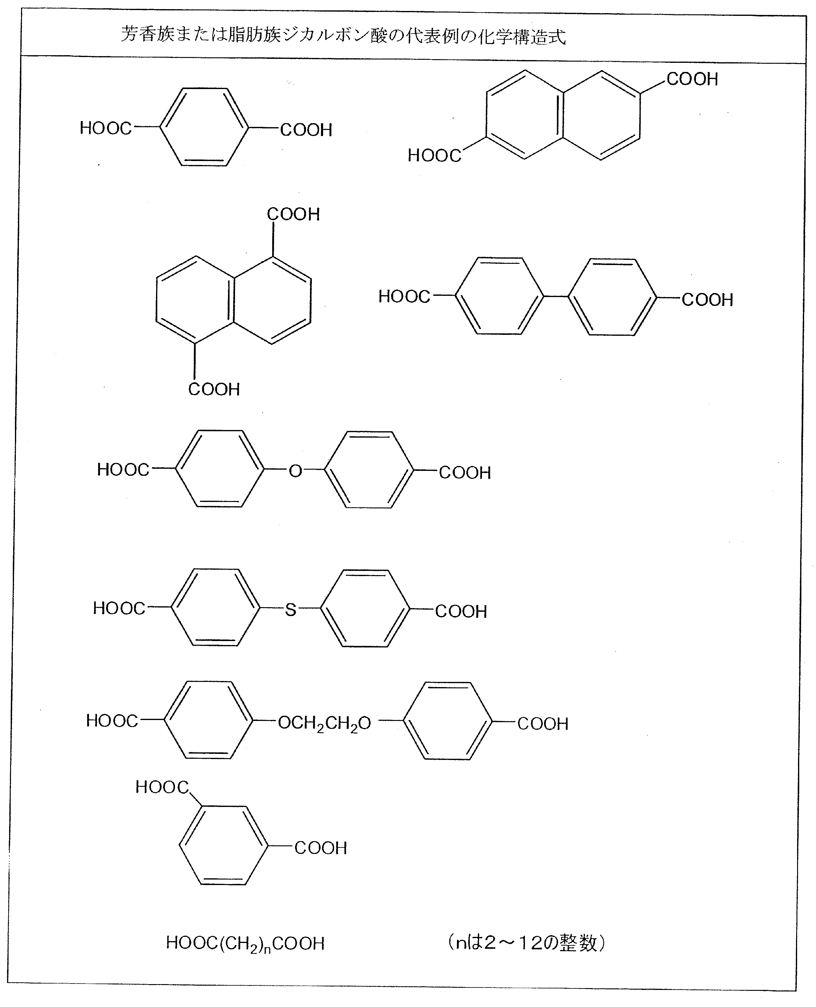
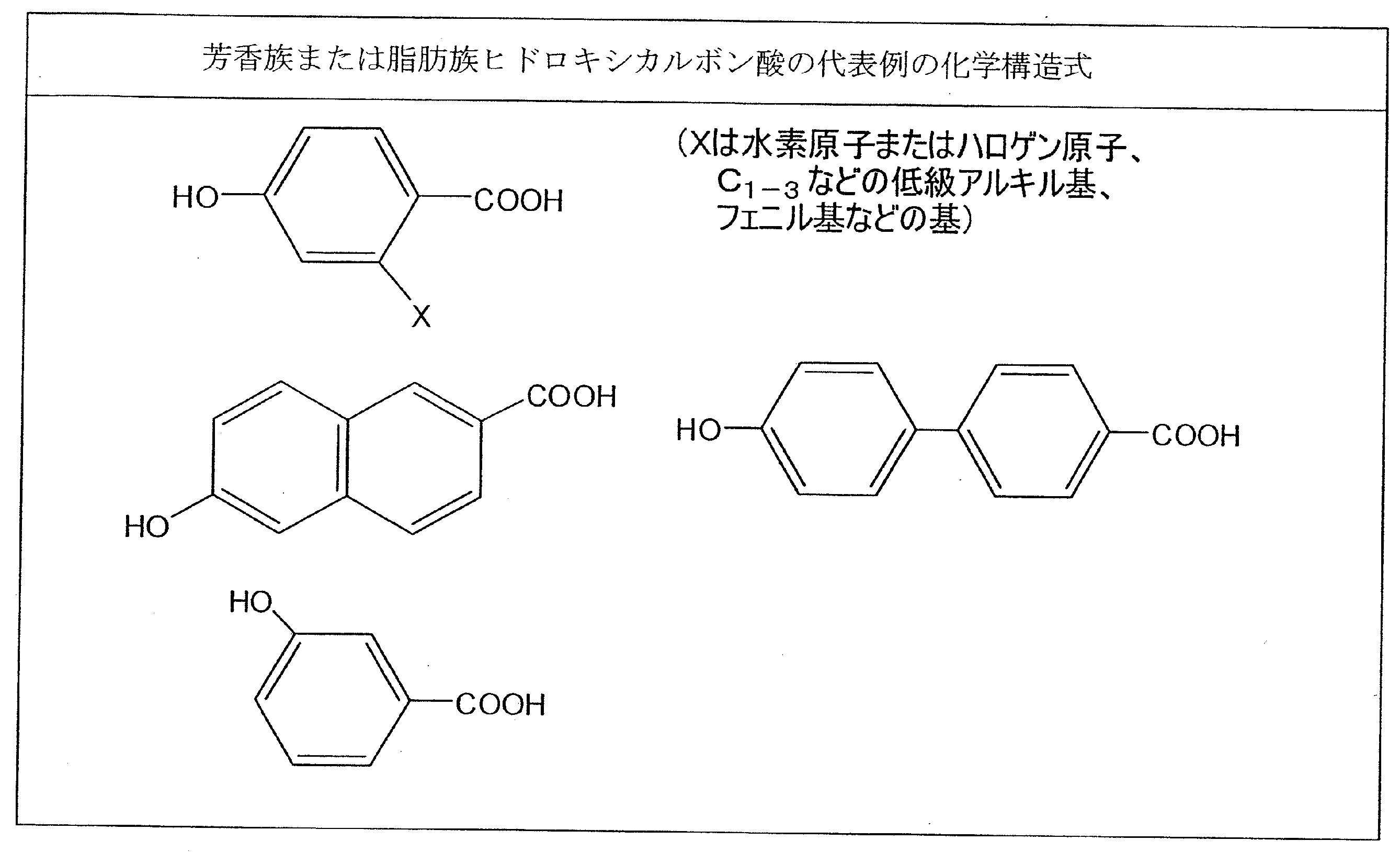
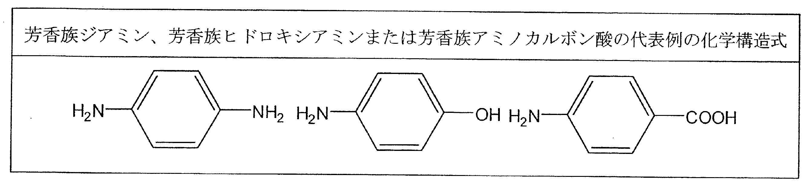
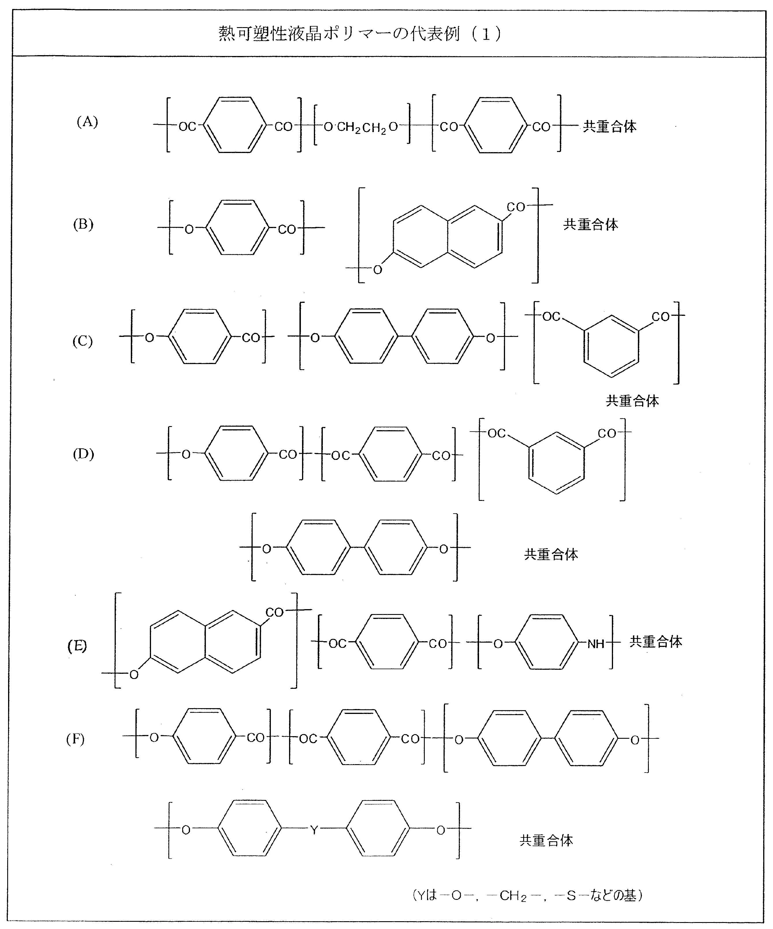
- thermoplastic liquid crystal polymer used in the present invention include known thermoplastic liquid crystal polyesters and thermoplastic liquid crystal polyester amides derived from the compounds (1) to (4) listed below and derivatives thereof. Can be mentioned. However, it goes without saying that there is an appropriate range of combinations of various raw material compounds in order to form a polymer capable of forming an optically anisotropic melt phase.
- Aromatic or aliphatic dihydroxy compounds (see Table 1 for typical examples)
- Aromatic diamine, aromatic hydroxyamine or aromatic aminocarboxylic acid (see Table 4 for typical examples)
- a polymer containing p-hydroxybenzoic acid and / or 6-hydroxy-2-naphthoic acid as at least a repeating unit is preferable.
- at least one aromatic hydroxycarboxylic acid selected from the group consisting of p-hydroxybenzoic acid and 6-hydroxy-2-naphthoic acid and 4,4 ′ A repeating unit of at least one aromatic diol selected from the group consisting of dihydroxybiphenyl and hydroquinone and at least one aromatic dicarboxylic acid selected from the group consisting of terephthalic acid, isophthalic acid and 2,6-naphthalenedicarboxylic acid Polymers containing are preferred.
- the repeating unit (A) of p-hydroxybenzoic acid is used.
- At least one aromatic hydroxycarboxylic acid (C) selected from the group consisting of p-hydroxybenzoic acid and 6-hydroxy-2-naphthoic acid, and 4,4′-dihydroxy At least one aromatic diol (D) selected from the group consisting of biphenyl and hydroquinone, and at least one aromatic dicarboxylic acid (E) selected from the group consisting of terephthalic acid, isophthalic acid and 2,6-naphthalenedicarboxylic acid.
- optical anisotropy at the time of melting referred to in the present invention can be recognized by, for example, placing a sample on a hot stage, heating and heating in a nitrogen atmosphere, and observing the transmitted light of the sample.
- the thermoplastic liquid crystal polymer preferably has a melting point (hereinafter referred to as Tm) in the range of 260 to 360 ° C., more preferably Tm of 270 to 350 ° C.
- Tm is calculated
- thermoplastic liquid crystal polymer a thermoplastic polymer such as polyethylene terephthalate, modified polyethylene terephthalate, polyolefin, polycarbonate, polyarylate, polyamide, polyphenylene sulfide, polyester ether ketone, fluororesin, etc., within the range not impairing the effects of the present invention, Various additives, fillers and the like may be added.
- thermoplastic liquid crystal polymer film used in the present invention can be obtained by extruding a thermoplastic liquid crystal polymer.
- any extrusion method such as the well-known T-die method or laminate stretching method can be applied, but the inflation method is particularly preferable.
- the extrusion process is performed by combining the following steps from the first step to the fifth step, thereby controlling the molecular structure of the liquid crystal polymer and producing a film having a small change in dielectric properties due to heating. be able to.
- thermoplastic liquid crystal polymer is melt extruded from the die by controlling the shear rate of the thermoplastic liquid crystal polymer during melt extrusion.
- the die shear rate that the thermoplastic liquid crystal polymer undergoes in the die region during melt extrusion from the die (sometimes simply referred to as shear rate) is 200 seconds ⁇ 1 or more (depending on the thickness of the film formed) ( For example, it can be selected from about 200 to 5000 seconds- 1 ), preferably about 300 to 4000 seconds- 1 .
- the longitudinal and transverse stretching ratio in the cooling process after extrusion is controlled.
- a predetermined draw ratio corresponding to a stretching ratio in the MD direction
- a blow ratio stretch ratio in the TD direction
- the draw ratio at this time is, for example, 1.5 to 5, preferably as the ratio (Br / Dr) of the draw ratio between the draw ratio (or Dr) in the MD direction and the draw ratio (or Br) in the TD direction. May be about 2.0 to 4.5.
- the distortion present in the film is relaxed by thermally shrinking the film after extrusion.
- the thermoplastic liquid crystal polymer film has a thermal shrinkage of 1% or more in the width direction under tension (for example, about 2.0 to 3.0 kg / mm 2 in the MD direction), preferably 1.5% or more.
- Heat shrink preferably the upper limit of a thermal contraction rate is suitably determined according to a film, it is about 4% normally in the width direction.
- the set temperature of the hot air drying furnace when performing heat shrinkage may be, for example, about 200 to 290 ° C., preferably about 230 to 270 ° C.
- the film once heat-shrinked is further heated near the melting temperature to increase the molecular weight of the liquid crystal domains present in the film.
- an increase in the molecular weight of the liquid crystal domain can be grasped as an increase in the heat distortion temperature of the film itself.
- the film is once heat-treated as a composite laminated with an adherend (for example, a metal foil such as a copper foil or an aluminum foil) that can maintain the form during the heat treatment of the film.
- the adhesion between the film and the adherend is usually performed by thermocompression bonding such as a hot press or a hot roller.
- the thermal expansion coefficient of the film is the same as that of the adherend (for example, about 16 ⁇ 10 ⁇ 6 to 26 ⁇ 10 ⁇ 6 cm / cm / ° C.).
- the temperature near the melting point (Tm) of the film that is, within the range of Tm ⁇ 30 (° C.) to Tm + 10 (° C.), preferably within the range of Tm ⁇ 25 (° C.) to Tm + 5 (° C.).
- Heat for 4 to 12 hours preferably about 5 to 10 hours.
- the thermal deformation temperature of the film is increased by, for example, about 40 to 80 ° C., preferably about 50 to 60 ° C., from the thermal deformation temperature of the raw film.
- the internal strain of the obtained film is relaxed by annealing treatment. Specifically, after peeling the film from the adherend, the thermoplastic liquid crystal polymer film is heated at a temperature 90 ° C. lower than the thermal deformation temperature (Td) of the film (Td ⁇ 90 ° C.) to a temperature 10 ° C. lower than Td ( Td-10 ° C.) is continuously supplied to a hot air drying furnace and heated for about 5 to 60 seconds, and the internal strain is about 0.3 to 3%, preferably 0.5 to 2.5. Remove about%.
- Td thermal deformation temperature
- thermoplastic liquid crystal polymer film of the present invention is a thermoplastic polymer, it can control the change in molecular orientation before and after heating, so that it has a high frequency range of 1 to 100 GHz.
- the change rate of the relative dielectric constant ( ⁇ r2 ) after heating the film with respect to the relative dielectric constant ( ⁇ r1 ) before heating the film changes only by 5% or less before and after heating.
- the film is heated in the range of a temperature 30 ° C. lower than the melting point of the film to a temperature 10 ° C. higher than the melting point, for example, for at least 1 hour (for example, 2 hours).
- the following formula (I) is satisfied with respect to the relative dielectric constant before and after heating.
- ⁇ r1 is a relative dielectric constant before heating the film
- ⁇ r2 is a relative dielectric constant ⁇ r2 after heating the film, and these relative dielectric constants are in the range of 1 to 100 GHz. Measured at the same frequency within.
- the relative dielectric constant is a value measured by the method described in Examples described later.
- the dielectric constant ( ⁇ r2 ) after heating of the thermoplastic liquid crystal polymer film at a frequency of 1 to 100 GHz may be, for example, 2.6 to 3.5, more preferably 2.6 to It may be 3.4.
- the dielectric loss tangent (Tan ⁇ 2 ) after heating of the thermoplastic liquid crystal polymer film may be, for example, 0.001 to 0.01, and more preferably 0.001 to 0.00. It may be 008.
- the specific dielectric constant ( ⁇ r2 ) and dielectric loss tangent (Tan ⁇ 2 ) of the thermoplastic liquid crystal polymer film after heating both show the above values in the temperature range of ⁇ 100 to 100 ° C. May be.
- the dielectric constant ( ⁇ r2 ) and dielectric loss tangent (Tan ⁇ 2 ) of the thermoplastic liquid crystal polymer film after heating are both after being exposed to 25 ° C. and 50% RH and 85 ° C. and 85% RH conditions. Even if it exists, the above-mentioned value may be shown.
- the thermoplastic liquid crystal polymer film used in the present invention may have any thickness, and includes a plate or sheet of 5 mm or less. However, when it is used for a high-frequency transmission line, the transmission loss decreases as the thickness increases, so it is necessary to increase the thickness as much as possible. However, when a thermoplastic liquid crystal polymer film is used alone as the electrical insulating layer, the film thickness is preferably in the range of 10 to 500 ⁇ m, and more preferably in the range of 15 to 200 ⁇ m. When the thickness of the film is too thin, the rigidity and strength of the film are reduced. Therefore, a method of obtaining an arbitrary thickness by laminating films having a film thickness in the range of 10 to 200 ⁇ m may be used.
- the laminate of the present invention comprises at least one film layer made of the thermoplastic polymer film and at least one metal layer, and has a laminated structure in which the film layers and metal layers are alternately laminated.
- the thermoplastic polymer films forming each film layer may have the same melting point or may have different melting points.
- the laminate can be produced by adhering a metal layer to at least one surface of the thermoplastic polymer film by thermocompression bonding.
- the laminate may be a single layer laminate having a single metal layer or a multilayer laminate having a plurality of metal layers.
- the gold used in the metal layer is preferably a metal used for electrical connection, and examples thereof include copper, gold, silver, nickel, and aluminum. Among these, copper is preferable.
- the thickness of the metal layer is preferably in the range of 1 to 50 ⁇ m, more preferably in the range of 5 to 20 ⁇ m.
- thermoplastic liquid crystal polymer film of the present invention can be directly thermocompression bonded to an ultra-low profile metal, and the surface roughness of such a metal layer is the thickness of the film on the surface facing the film. 1/50 or less, preferably 1/60 or less, more preferably 1/70 or less.
- the specific surface roughness may be, for example, 5 ⁇ m or less, preferably 3 ⁇ m or less.
- the rate of change of the relative dielectric constant ( ⁇ r3 ) of the laminate after thermocompression bonding relative to the relative dielectric constant ( ⁇ r1 ) of the film before thermocompression satisfies the following formula (II).
- the relative dielectric constant is a value measured by the method described in Examples described later.
- the dielectric constant ( ⁇ r3 ) of the laminate after thermocompression bonding may be, for example, 2.6 to 3.5, and more preferably 2.6 to 3. 4 may be sufficient.
- the dielectric loss tangent (Tan ⁇ 3 ) of the laminate after thermocompression bonding may be, for example, 0.001 to 0.01, and more preferably 0.001 to 0.008. There may be.
- the relative permittivity ( ⁇ r3 ) and dielectric loss tangent (Tan ⁇ 3 ) after thermocompression bonding of the laminate both show the above values in the temperature range of ⁇ 100 to 100 ° C. Good.
- the dielectric constant ( ⁇ r3 ) and dielectric loss tangent (Tan ⁇ 3 ) after thermocompression bonding of the laminate are both after being exposed to 25 ° C. 50% RH and 85 ° C. 85% RH conditions. May show the above-mentioned values.
- Such a laminate can be manufactured using a thermocompression bonding method such as a hot press and a heat roller as long as the dielectric properties of the thermoplastic liquid crystal polymer film do not change. Recently, a novel method for efficiently producing a laminate or a circuit board has been found.
- the production method includes (i) a metal laminated film preparation step of preparing a metal laminated film in which a metal layer is thermocompression bonded to at least one surface of the liquid crystal polymer film according to any one of claims 1 to 4, (Ii) A substrate set obtained by stacking a plurality of the metal laminated films or at least one metal laminated film and at least one thermoplastic liquid crystal polymer film in a state where film layers and metal layers are alternately laminated.
- a method for producing a laminate comprising: In the manufacturing method, the heating / pressing plate has a minute convex portion for absorbing thermal expansion of the metal layer.
- the heating and pressurizing plate since the heating and pressurizing plate has minute convex portions for absorbing the thermal expansion of the metal layer, conventionally, the thermal expansion of the metal layer, which has been necessary when performing hot pressing with the heating and pressing platen. There is no need to use an absorbent member, the thermal conductivity during hot pressing is improved, and the hot pressing cycle time can be significantly shortened compared to the prior art.
- the minute protrusions can be set as appropriate according to the coefficient of thermal expansion of the metal layer.
- the minute protrusions are end portions of the heating and pressing plate on the substrate set side.
- the convex portion that rises from the center toward the center, and the height at the center may be, for example, about 10 to 500 ⁇ m, preferably about 100 to 200 ⁇ m.
- the manufacturing method of the said laminated body can be effectively utilized with respect to the specific thermoplastic liquid crystal polymer film of this invention, and the commercially available thermoplastic liquid crystal used conventionally can be shortened in the point which can shorten a hot press cycle. It can also be effectively used for polymer films (for example, the Bexter series marketed by Kuraray Co., Ltd.).
- the circuit board includes at least a thermoplastic liquid crystal polymer film and a conductor circuit layer formed on at least one surface of the thermoplastic liquid crystal polymer film.
- the conductor circuit can be formed according to a known method. Specific examples include (a) a method of forming a conductor circuit by laminating a thermoplastic liquid crystal polymer film and a metal layer by thermocompression bonding, and then performing an etching process, etc., (b) the surface of the thermoplastic liquid crystal polymer film. And a method of forming a conductor layer by a vapor phase method such as a sputtering method, an ion plating method, a vacuum deposition method or a wet plating method to form a conductor circuit.
- a vapor phase method such as a sputtering method, an ion plating method, a vacuum deposition method or a wet plating method to form a conductor circuit.
- metal material used for forming the metal layer or conductor circuit layer
- various metals described in the above metal layer can be used.
- the manufacturing method of the said laminated body can be utilized as a method of manufacturing a circuit board, In this case, except using the metal laminated
- the circuit board may be a single-layer circuit board provided with a single metal layer (or conductor circuit layer). However, in order to satisfy the demand for higher functionality of the circuit board, a plurality of metal layers (or conductive pattern layers) are used. Is preferably a multilayer circuit board (for example, a two-layer circuit board, a three-layer circuit board, a four-layer circuit board, etc.). In this case, the metal layer patterned as necessary on the circuit board is used as a signal line or a ground plane line having a predetermined pattern.
- the circuit board Since the circuit board has a stable relative dielectric constant before and after heating even in the high frequency region, it can be used as a high frequency circuit board.
- the high-frequency circuit board is not only composed of a circuit that transmits only a high-frequency signal, but also a transmission path for converting a high-frequency signal to a low-frequency signal and outputting the generated low-frequency signal to the outside, or a high-frequency compatible component
- a transmission path for transmitting a signal that is not a high-frequency signal, such as a transmission path for supplying power supplied for driving, is also included on the same plane.
- transmission lines include various transmission lines, for example, known or common transmission lines such as a coaxial line, a strip line, a microstrip line, a coplanar line, and a parallel line.
- known or common transmission lines such as a coaxial line, a strip line, a microstrip line, a coplanar line, and a parallel line.
- the film was obtained by observing the thermal behavior of the film using a differential scanning calorimeter. In other words, the sample film was heated at a rate of 20 ° C./min to be completely melted, and then the melt was rapidly cooled to 50 ° C. at a rate of 50 ° C./min, and again raised at a rate of 20 ° C./min. The position of the endothermic peak that appeared when the film was recorded was recorded as the melting point of the film.
- Heat shrinkage rate was calculated by the following equation after measuring the dimensions of the test piece before and after the heat shrinkage with a caliper.
- thermomechanical analyzer TMA
- a tensile load of 1 g was applied to both ends of a film having a width of 5 mm and a length of 20 mm, and the temperature was increased from room temperature at a rate of 5 ° C./min until the film was broken. This is the temperature at which sudden expansion (elongation) has occurred, and the temperature at the intersection of the tangent line of the high temperature side base line and the low temperature side base line in the temperature to deformation curve is defined as the heat deformation temperature.
- the film thickness was measured using a digital thickness meter (manufactured by Mitutoyo Corporation) at a 1 cm interval in the TD direction, and the average value of 10 points arbitrarily selected from the center and the edge was taken as the film thickness. .
- the surface roughness (Rz) of the copper foil was measured at a measurement magnification of 1000 using a shape measuring microscope (manufactured by Keyence Corporation, model: VK-810). The measurement was performed by a method based on JIS B0601-1994.
- surface roughness (Rz) the reference length is extracted from the roughness curve in the direction of the average line, the average value of the altitude of the highest peak to the fifth peak (convex peak), and the bottom from the deepest to the fifth peak. The difference from the average value of the altitude of (concave bottom) is expressed in ⁇ m, and the ten-point average roughness is shown.
- the dielectric constant was measured by a resonance perturbation method at a frequency of 10 GHz.
- a 1 GHz cavity resonator (Kanto Electronics Co., Ltd.) was connected to a network analyzer (Agilent Technology “E8362B”), and a minute material (width: 2.7 mm ⁇ length: 45 mm) was connected to the cavity resonator.
- the dielectric constant and dielectric loss tangent of the material were measured from the change in resonance frequency before and after insertion for 96 hours in an environment of temperature 20 ° C. and humidity 65% RH.
- a test specimen for peeling having a width of 1.0 cm is prepared from a laminate of a liquid crystal polymer film and a metal layer, the liquid crystal polymer film is fixed to a flat plate with a double-sided adhesive tape, and the laminate is obtained by a 180 ° method according to JIS C 5016. Was peeled at a speed of 50 mm / min, and the strength (kN / m) was measured.
- Example 1 Thermotropic liquid crystal polyester [VECTRA A950 (trade name), Polyplastics Co., Ltd.] was heated and kneaded with a single screw extruder, die diameter 33.5 mm, an annular inflation die die slit interval 500 [mu] m, the die shear rate of 1000 sec - 1 was melt-extruded (first step), and then stretched so that the ratio (Br / Dr) of the stretch ratio (or Br) in the TD direction to the stretch ratio (or Dr) in the MD direction was 3 (second) Process). Subsequently, the obtained raw film (melting point: 280 ° C.) was heated in a hot air drying furnace set at 260 ° C.
- thermoplastic liquid crystal polymer film was once thermally bonded to an aluminum foil having a thickness of 50 ⁇ m to form a composite, which was heated in a hot air oven controlled at 270 ° C. for 30 seconds, and had a thermal expansion coefficient of 18 ⁇ 10 ⁇ 6 cm. Then, this composite is supplied to a hot-air circulating heat treatment furnace controlled to 270 ° C. (Tm ⁇ 10 ° C. of the raw film) for 10 hours, whereby the heat of the thermoplastic liquid crystal polymer film is changed. The deformation temperature was increased by 80 ° C. (fourth step).
- this film was supplied at a rate of 1 m / min to a hot air circulation type heat treatment furnace having a furnace length of 1 m controlled at 200 ° C. (Td-60 ° C. of the raw film). Heat treatment was performed to remove 1% of internal strain (fifth step). The obtained film had a relative dielectric constant of 3.3 measured at 1 to 100 GHz.
- Example 2 Thermotropic liquid crystal polyester [VECTRA A950 (trade name), Polyplastics Co., Ltd.] was heated and kneaded with a single screw extruder, die diameter 33.5 mm, an annular inflation die die slit interval 350 .mu.m, the die shear rate 2000 sec - 1 was melt-extruded (first step), and then stretched so that the ratio (Br / Dr) of the stretch ratio (or Br) in the TD direction to the stretch ratio (or Dr) in the MD direction was 4 (second) Process). Subsequently, the obtained raw film (melting point: 280 ° C.) was heated in a hot air drying furnace set at 260 ° C.
- thermoplastic liquid crystal polymer film was once thermally bonded to an aluminum foil having a thickness of 50 ⁇ m to form a composite, which was heated in a hot air oven controlled at 270 ° C. for 10 seconds, and had a thermal expansion coefficient of 10 ⁇ 10 ⁇ 6 cm. / Cm / ° C. Subsequently, this composite was supplied to a hot-air circulating heat treatment furnace controlled at 260 ° C. (Tm ⁇ 20 ° C. of raw film) for 8 hours, thereby increasing the thermal deformation temperature of the thermoplastic liquid crystal polymer film by 40 ° C. (Fourth step).
- this film was supplied at a rate of 1 m / min to a hot air circulation type heat treatment furnace having a furnace length of 1 m controlled at 230 ° C. (Td-30 ° C. of the raw film). Heat treatment was performed to remove 2% of internal strain (fifth step). The obtained film had a relative dielectric constant of 3.1 measured at 1 to 100 GHz.
- thermoplastic liquid crystal polymer film was once thermally bonded to an aluminum foil having a thickness of 50 ⁇ m to form a composite, and heated in a hot air oven controlled at 260 ° C. for 30 seconds, so that the thermal expansion coefficient was 10 ⁇ 10 ⁇ 6 cm. / Cm / ° C.
- the obtained film had a relative dielectric constant of 3.0 measured at 1 to 100 GHz.
- thermoplastic liquid crystal polymer film was once thermally bonded to an aluminum foil having a thickness of 50 ⁇ m to form a composite, which was heated in a hot air oven controlled at 280 ° C. for 30 seconds, and had a thermal expansion coefficient of 10 ⁇ 10 ⁇ 6 cm. / Cm / ° C. Subsequently, the composite was supplied to a hot-air circulating heat treatment furnace controlled at 280 ° C. (Tm-40 ° C. of the raw film) for 6 hours, thereby increasing the thermal deformation temperature of the thermoplastic liquid crystal polymer film by 40 ° C. (Fourth step). The obtained film had a relative dielectric constant of 3.2 measured at 1 to 100 GHz.
- the films obtained in Examples and Comparative Examples were heated at the melting point of the obtained film for 60 minutes, and the relative dielectric constant and dielectric loss tangent were measured in the temperature range of ⁇ 100 to 100 ° C. Furthermore, the heated film was further allowed to stand at 25 ° C., 50% RH and 85 ° C., 85% RH for 96 hours, and the relative dielectric constant and dielectric loss tangent of the film after being left standing were measured.
- Table 7 shows the physical properties of the films obtained in Examples and Comparative Examples.
- thermoplastic liquid crystal polymer films of Examples 1 and 2 have almost no change in relative dielectric constant before and after heating.
- the relative dielectric constant after heating is greatly changed as compared with before heating.
- the films of Examples 1 and 2 maintain a low relative dielectric constant and dielectric loss tangent under a wide temperature range and high temperature / high humidity conditions even after heating.
- the dielectric constant and dielectric loss tangent after heating are increased. Moreover, these dielectric properties are further deteriorated under high temperature and high humidity conditions.
- Example 3 A 18 ⁇ m thick copper foil (copper foil roughness: 3 ⁇ m) was superimposed on both surfaces of the thermoplastic liquid crystal polymer film produced in Example 1, and the temperature was 300 ° C. and the pressure was 30 kg / pressure using a vacuum hot press apparatus. A metal laminated film composed of a thermoplastic liquid crystal polymer film and a copper foil was produced by thermocompression bonding under the conditions of cm 2 . Next, the film produced in Example 1 was sandwiched between two metal laminated films as an intermediate sheet, and 10 sets were prepared on a heating and pressing panel. The heating / pressing plate has a gentle convex portion from the end portion toward the central portion on the substrate set side, and the height of the convex portion at the central portion is about 100 ⁇ m.
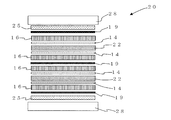
- each substrate set 12 is set in the thermocompression bonding apparatus 10 in a state where it is sandwiched between heating and pressurizing panels 18 and 18 via a release material 14 and a cushion material 16 on the outside. Further, the stainless plates 19, 19 are disposed only on the heating and pressurizing plate side, and are disposed so as to sandwich all the base material sets.
- the substrate set 12 was quickly heated to 295 ° C., and a plurality of multilayer laminates were formed in a total press time of 30 minutes.
- the interfacial adhesive strength of the obtained multilayer laminate was 0.8 kN / m.
- thermocompression bonding apparatus 20 As a thermoplastic liquid crystal polymer film, the same number of substrates as in Example 3 was prepared in the same manner as in Example 3 except that Comparative Example 1 was used. Next, as shown in FIG. 2, each substrate set 22 is set in the thermocompression bonding apparatus 20 in a state of being sandwiched between the heating and pressurizing panels 28 and 28 via the release material 14, the cushioning material 16 and the stainless steel plate 19 on the outside. did.
- the heating / pressing plate 28 does not have fine convex portions.
- a press pad 25 for correcting the distortion of the copper foil is disposed so as to sandwich all the base material sets only on the heating and pressurizing board side. Further, in order to correct the distortion of the copper foil, the stainless steel plate 19 is inserted between the cushion materials between the substrate sets, and the cushion material 16 is disposed on both sides of the stainless steel plate 19.
- the third comparative example unlike the third embodiment, requires not only a stainless steel plate between each substrate set, but also a press pad. It took time for the temperature of 22 to rise to 295 ° C., and the total press time for forming a plurality of multilayer laminates was 120 minutes. The interfacial adhesive strength of the resulting multilayer laminate is It was 0.8 kN / m.
- Example 3 and Comparative Example 3 The relative dielectric constant and dielectric loss tangent of the multilayer laminate obtained in Example 3 and Comparative Example 3 were measured in the temperature range of ⁇ 100 to 100 ° C. Further, the multilayer laminate was further allowed to stand for 96 hours at 25 ° C. and 50% RH and 85 ° C. and 85% RH, respectively, and the relative dielectric constant and dielectric loss tangent of the multilayer laminate were measured. Table 8 shows the physical properties of the multilayer laminate obtained in Example 3 and Comparative Example 3.
- the relative dielectric constant of the thermoplastic liquid crystal polymer film of Example 3 hardly changed before and after heating. Further, even when an ultra low profile copper foil was used, the thermoplastic liquid crystal polymer did not flow out of the multilayer laminate. On the other hand, in the multilayer laminate of Comparative Example 3, the relative dielectric constant after heating is greatly changed compared to before heating. Moreover, since the ultra low profile copper foil was used, the thermoplastic liquid crystal polymer flowed out of the multilayer laminate.
- thermoplastic liquid crystal polymer film of Comparative Example 1 when the hot pressing is performed in the same manner as in Example 3 except that the thermoplastic liquid crystal polymer film of Comparative Example 1 is used instead of the thermoplastic liquid crystal polymer film of Example 1, an ultra-low profile is obtained. Even if it is copper foil, a multilayer laminated board can be produced efficiently without flowing out.
- thermoplastic liquid crystal polymer film of the present invention can be used as a substrate material for electric / electronic products. Moreover, according to this invention, a board
Landscapes
- Chemical & Material Sciences (AREA)
- Engineering & Computer Science (AREA)
- Manufacturing & Machinery (AREA)
- Microelectronics & Electronic Packaging (AREA)
- Organic Chemistry (AREA)
- Materials Engineering (AREA)
- Health & Medical Sciences (AREA)
- Chemical Kinetics & Catalysis (AREA)
- Medicinal Chemistry (AREA)
- Polymers & Plastics (AREA)
- Crystallography & Structural Chemistry (AREA)
- Laminated Bodies (AREA)
- Manufacture Of Macromolecular Shaped Articles (AREA)
- Production Of Multi-Layered Print Wiring Board (AREA)
Abstract
Description
この文献では、光学的異方性の溶融相を形成し得るポリマーから作製されるフィルムと被着体との積層体が複数、熱圧着によって接合されており、接合された状態で隣接する一方の積層体の被着体と、他方の積層体の被着体とが相対向している場合には、両者の間に光学的異方性の溶融相を形成し得るポリマーから作製されるフィルムからなる中間シートが介装されており、前記積層体のフィルムおよび中間シートは、同一化学組成であり、かつ隣接するフィルムおよび中間シートに、互いに異なる耐熱性が付与されていることを特徴とする多層積層板が開示されている。
この文献には、光学的異方性の溶融相を形成し得る熱可塑性ポリマーからなるフィルム(以下、これを熱可塑性液晶ポリマーフィルムと称する)と金属箔とからなる構成材料を重ね合せて平坦な金属プレート間に挟んだ構成のセットを複数セット積み重ね、対向する加熱加圧盤間に装着し、加熱プレスして金属箔積層板を製造する方法において、対向する加熱加圧盤間に装着した後に、(1)加圧することなく、熱可塑性液晶ポリマーフィルムの融点より30℃低い温度を上限とする予熱温度まで加熱する予熱工程である第1工程、(2)2kg/cm2以下のプレス圧力を保ちながら、予熱温度から、熱可塑性液晶ポリマーフィルムの融点より5℃低い温度以上融点より5℃高い温度以下の範囲から選択される積層温度まで加熱する昇温工程である第2工程、(3)積層温度で、20kg/cm2から50kg/cm2までの範囲から選択されるプレス圧力にまで加圧する加圧工程である第3工程、および(4)加圧工程のプレス圧力を保ちながら、熱可塑性液晶ポリマーフィルムの融点より30℃以上低い冷却温度まで冷却する冷却工程である第4工程を行い、その際に、第2工程から第4工程までを30分以内の時間で行い、かつ第1工程から第4工程までを30torr以下の減圧状態で行い、次いで(5)加圧および減圧状態を解除して、金属箔積層板を取り出す排出工程である第5工程を行うことを特徴とする金属箔積層板の製造方法が開示されている。
本発明の別の目的は、前記目的に加えて、温度・水分環境が変動した場合、特に、高温および/または高湿条件下にフィルムを曝した場合であっても、優れた誘電特性を示す熱可塑性液晶ポリマーフィルムを提供することにある。
本発明の他の目的は、このような積層体または回路基板を効率よく製造する方法を提供することにある。
1~100GHzの周波数において、フィルムを加熱する前の比誘電率(εr1)に対するフィルムを加熱した後の比誘電率(εr2)の変化率が、フィルムを該フィルムの融点よりも30℃低い温度から融点より10℃高い温度の範囲で1時間加熱した場合に、下記式(I)を満たす熱可塑性液晶ポリマーフィルムである。
|εr2-εr1|/εr1×100≦5 (I)
(式中、εr1は、フィルムを加熱する前の比誘電率であり、εr2は、フィルムを加熱した後の比誘電率であり、これらの比誘電率は、同一の周波数において測定される。)
(I)熱可塑性液晶ポリマーを溶融押出する工程であって、ダイから溶融押出する際に熱可塑性液晶ポリマーがダイ領域で受けるダイ剪断速度を200秒-1以上とする溶融押出工程、
(II)押出後の冷却過程で、MD方向の延伸比(またはドロー比:Dr)に対するTD方向の延伸比(またはブロー比:Br)の延伸倍率の比(Br/Dr)を、1.5~5として延伸を行う延伸工程、
(III)押出成形後の原反フィルムを、張力下で1.5%以上、熱収縮させる熱収縮工程、
(VI)熱収縮させたフィルムを、被着体と積層した複合体としてフィルムの熱膨張係数を制御した後、フィルムの融点(Tm)から10℃低い温度(Tm-10℃)~Tmから10℃高い温度(Tm+10℃)の範囲内で加熱してフィルムの熱変形温度(Td)を増加させる熱処理工程、および
(V)熱処理後に被着体から剥離したフィルムに対して、原反フィルムの熱変形温度(Td)から80℃低い温度(Td-80℃)~Tdから10℃低い温度(Td-10℃)の範囲内で加熱してフィルムのアニール処理を行うアニール工程、
を少なくとも備える熱可塑性液晶ポリマーフィルムの製造方法である。
を少なくとも含む回路基板を包含する。なお、この回路基板は、複数の導体回路層を備えていてもよい。
(i)請求項1~4のいずれか一項に記載の液晶ポリマーフィルムの少なくとも一方の面に金属層が熱圧着された金属積層フィルムを準備する金属積層フィルム準備工程と、
(ii)複数の前記金属積層フィルム同士を、または少なくとも一つの金属積層フィルムと少なくとも一つの熱可塑性液晶ポリマーフィルムとを、フィルム層と金属層とが交互に積層した状態で積み重ねた基板セットを、少なくとも1セット準備して、対向する加熱加圧盤間に装着する基板セット装着工程と、
(iii)前記加熱加圧盤を加熱して、前記装着された基板セットを熱圧着によって接合する接合工程と、
を含む積層体の製造方法であって、
前記加熱加圧盤は、金属層の熱膨張を吸収するための微小凸部を有している。
|εr2-εr1|/εr1×100≦5 (I)
(式中、εr1は、フィルムを加熱する前の比誘電率であり、εr2は、フィルムを加熱した後の比誘電率εr2であり、これらの比誘電率は、同一の周波数において測定される。)
前記熱可塑性液晶ポリマーフィルムは、溶融成形できる液晶性ポリマー(または光学的に異方性の溶融相を形成し得るポリマー)で構成され、この熱可塑性液晶ポリマーは、溶融成形できる液晶性ポリマーであれば特にその化学的構成については特に限定されるものではないが、例えば、熱可塑性液晶ポリエステル、又はこれにアミド結合が導入された熱可塑性液晶ポリエステルアミドなどを挙げることができる。


第一工程では、溶融押出時の熱可塑性液晶ポリマーへの剪断速度を制御して、ダイから熱可塑性液晶ポリマーを溶融押出する。この際、ダイから溶融押出する際に熱可塑性液晶ポリマーがダイ領域で受けるダイ剪断速度(単に、剪断速度と称する場合がある)は、製膜する厚みなどに応じて、200秒-1以上(例えば、200~5000秒-1程度)、好ましくは300~4000秒-1程度から選択することができる。
第二工程では、押出後の冷却過程での縦横延伸比率を制御する。ダイから溶融押出されたシート(特に、リングダイを用いた場合には、円筒状シート)に対して、所定のドロー比(MD方向の延伸倍率に相当する)およびブロー比(TD方向の延伸倍率に相当する)で延伸を行う。この際の延伸倍率は、MD方向の延伸倍率(またはDr)とTD方向の延伸倍率(またはBr)とのそれぞれの延伸倍率の比(Br/Dr)として、例えば、1.5~5、好ましくは2.0~4.5程度であってもよい。
第三工程では、押出成形後のフィルムを、熱収縮させることによって、フィルム内部に存在する歪みを緩和させる。
この際、熱可塑性液晶ポリマーフィルムは、張力下(例えば、MD方向に2.0~3.0kg/mm2程度)で、幅方向に1%以上の熱収縮、好ましくは1.5%以上、熱収縮させる。なお、熱収縮率の上限は、フィルムに応じて適宜決定されるが、通常幅方向で4%程度である。熱収縮を行う際の熱風乾燥炉の設定温度は、例えば200~290℃程度、好ましくは230~270℃程度であってもよい。
そして、第四工程では、一旦熱収縮させたフィルムを、更に溶融温度付近で加熱することによって、フィルム内部に存在する液晶ドメインの分子量を増加させる。このような液晶ドメインの分子量の増加は、フィルム自体の熱変形温度の増大として把握することができる。この場合、フィルムは、一旦、該フィルムの熱処理時に形態を保持し得る被着体(例えば、銅箔、アルミニウム箔などの金属箔)と積層した複合体として熱処理を行う。フィルムと被着体の接着は、通常、熱プレス、熱ローラー等の熱圧着によって行われる。このような複合体は、フィルムの熱膨張係数が被着体の熱膨張係数と同じ熱膨張係数(たとえば、16×10-6~26×10-6cm/cm/℃程度)になるように熱処理を行った後、フィルムの融点(Tm)付近の温度、すなわち、Tm-30(℃)~Tm+10(℃)の範囲内、好ましくはTm-25(℃)~Tm+5(℃)の範囲内において4~12時間、好ましくは5~10時間程度加熱させる。その結果、フィルムの熱変形温度は、原反フィルムの熱変形温度より、例えば、40~80℃程度、好ましくは、50~60℃程度上昇する。
第五工程では、アニール処理によって、得られたフィルムの内部歪みの緩和を行なう。具体的には、被着体からフィルムを剥がした後、この熱可塑性液晶ポリマーフィルムを、フィルムの熱変形温度(Td)から90℃低い温度(Td-90℃)~Tdから10℃低い温度(Td-10℃)に制御した熱風乾燥炉に連続的に供給して、5~60秒間程度、加熱処理を行い、内部歪みを0.3~3%程度、好ましくは0.5~2.5%程度除去する。
|εr2-εr1|/εr1×100≦5 (I)
(式中、εr1は、フィルムを加熱する前の比誘電率であり、εr2は、フィルムを加熱した後の比誘電率εr2であり、これらの比誘電率は、1~100GHzの範囲内の同一の周波数において測定される。)
なお、ここで比誘電率は、後述する実施例に記載した方法により測定される値である。
本発明の積層体は、前記熱可塑性ポリマーフィルムからなる少なくとも1つのフィルム層と、少なくとも1つの金属層とを備え、前記フィルム層と金属層とが交互に積層した積層構造を有している。なお、フィルム層が複数存在する場合、各フィルム層を形成する熱可塑性ポリマーフィルムは、それぞれ同じ融点を有するものであってもよく、異なる融点を有するものであってもよい。
|εr3-εr1|/εr1×100≦5 (II)
(式中、εr1は、熱圧着前のフィルムの比誘電率であり、εr3は、フィルムと金属層との熱圧着後の比誘電率であり、これらの比誘電率は、1~100GHzの範囲内の同一の周波数において測定される。)
(ii)複数の前記金属積層フィルム同士を、または少なくとも一つの金属積層フィルムと少なくとも一つの熱可塑性液晶ポリマーフィルムとを、フィルム層と金属層とが交互に積層した状態で積み重ねた基板セットを、少なくとも1セット準備して、対向する加熱加圧盤間に装着する基板セット装着工程と、
(iii)前記加熱加圧盤を加熱して、前記装着された基板セットを熱圧着によって接合する接合工程と、
を含む積層体の製造方法であって、
前記加熱加圧盤が、金属層の熱膨張を吸収するための微小凸部を有している製造方法である。
回路基板は、熱可塑性液晶ポリマーフィルムと、前記熱可塑性液晶ポリマーフィルムの少なくとも一方の面に形成された導体回路層と、を少なくとも含んでいる。
示差走査熱量計を用いて、フィルムの熱挙動を観察して得た。つまり、供試フィルムを20℃/分の速度で昇温して完全に溶融させた後、溶融物を50℃/分の速度で50℃まで急冷し、再び20℃/分の速度で昇温した時に現れる吸熱ピークの位置を、フィルムの融点として記録した。
熱収縮率は、前記の熱収縮前後の試験片の寸法をノギスで測定し、次式により算出した。

熱機械分析装置(TMA)を用いて、幅5mm、長さ20mmのフィルムの両端に1gの引張荷重をかけ、室温から5℃/分の速度で、フィルムが破断するまで昇温したときの、急激な膨張(伸び)が発生した温度であり、温度~変形曲線における高温側のベースラインの接線と低温側のベースラインの接線の交点の温度を熱変形温度とする。
2次元測長器を用いて、加熱前の長さに対して加熱後の長さを測定し、次式により算出した。
内部歪み(%)=(加熱後の長さ-加熱前の長さ)/加熱後の長さ × 100
膜厚は、デジタル厚み計(株式会社ミツトヨ製)を用い、選られたフィルムをTD方向に1cm間隔で測定し、中心部および端部から任意に選んだ10点の平均値を膜厚とした。
形状測定顕微鏡(キーエンス(株)製、型式:VK-810) を用い、測定倍率1000倍で銅箔の表面粗度(Rz)を測定した。測定はJIS B0601―1994に準拠した方法により行った。表面粗度(Rz)は、粗さ曲線からその平均線の方向に基準長さを抜き取り、最高から5番目までの山頂(凸の頂点)の標高の平均値と、最深から5番目までの谷底(凹の底点)の標高の平均値との差をμmで表わしたもので、十点平均粗さを示している。
誘電率測定は周波数10GHzで共振摂動法により実施した。ネットワークアナライザ(Agilent Technology社製「E8362B」)に1GHzの空洞共振器((株)関東電子応用開発)を接続し、空洞共振器に微小な材料(幅:2.7mm×長さ:45mm)を挿入し、温度20℃、湿度65%RH環境下、96時間の挿入前後の共振周波数の変化から材料の誘電率および誘電正接を測定した。
液晶ポリマーフィルムと金属層との積層体から1.0cm幅の剥離用試験片を作製し、液晶ポリマーフィルムを両面接着テープで平板に固定し、JIS C 5016に準じて180°法により、積層体を50mm/分の速度で剥離したときの強度(kN/m)を測定した。
熱可塑性液晶ポリエステル〔ベクトラA950(商品名)、ポリプラスチックス社製〕を単軸押出機で加熱混練し、ダイ直径33.5mm、ダイスリット間隔500μmの環状インフレーションダイから、ダイ剪断速度1000秒-1で溶融押出し(第一工程)、その後MD方向の延伸倍率(またはDr)に対するTD方向の延伸倍率(またはBr)の比(Br/Dr)が3となるように延伸を行った(第二工程)。ついで、得られた原反フィルム(融点280℃)を張力下で260℃に設定した熱風乾燥炉で加熱することにより、2%熱収縮させた(第三工程)。さらに、この熱可塑性液晶ポリマーフィルムを、一旦、厚さ50μmのアルミニウム箔と熱接着させて複合体とし、270℃に制御した熱風炉で30秒間加熱し、熱膨張係数を18×10-6cm/cm/℃に変化させ、続いて、この複合体を270℃(原反フィルムのTm-10℃)に制御した熱風循環式熱処理炉に10時間供給することにより、熱可塑性液晶ポリマーフィルムの熱変形温度を80℃増大させた(第四工程)。そして、被着体からフィルムを剥がした後、このフィルムを、200℃(原反フィルムのTd-60℃)に制御した炉長1mの熱風循環式熱処理炉に1m/分の速度で供給して加熱処理を行い、内部歪みを1%除去した(第五工程)。得られたフィルムは、1~100GHzで測定された比誘電率が3.3であった。
熱可塑性液晶ポリエステル〔ベクトラA950(商品名)、ポリプラスチックス社製〕を単軸押出機で加熱混練し、ダイ直径33.5mm、ダイスリット間隔350μmの環状インフレーションダイから、ダイ剪断速度2000秒-1で溶融押出し(第一工程)、その後MD方向の延伸倍率(またはDr)に対するTD方向の延伸倍率(またはBr)の比(Br/Dr)が4となるように延伸を行った(第二工程)。ついで、得られた原反フィルム(融点280℃)を張力下で260℃に設定した熱風乾燥炉で加熱することにより、3%熱収縮させた(第三工程)。さらに、この熱可塑性液晶ポリマーフィルムを、一旦、厚さ50μmのアルミニウム箔と熱接着させて複合体とし、270℃に制御した熱風炉で10秒間加熱し、熱膨張係数を10×10-6cm/cm/℃に変化させた。続いて、この複合体を260℃(原反フィルムのTm-20℃)に制御した熱風循環式熱処理炉に8時間供給することにより、熱可塑性液晶ポリマーフィルムの熱変形温度を40℃増大させた(第四工程)。そして、被着体からフィルムを剥がした後、このフィルムを、230℃(原反フィルムのTd-30℃)に制御した炉長1mの熱風循環式熱処理炉に1m/分の速度で供給して加熱処理を行い、内部歪みを2%除去した(第五工程)。得られたフィルムは、1~100GHzで測定された比誘電率が3.1であった。
熱可塑性液晶ポリエステル〔ベクトラA950(商品名)、ポリプラスチックス社製〕を単軸押出機で加熱混練し、ダイ直径33.5mm、ダイスリット間隔500μmの環状インフレーションダイから、ダイ剪断速度1000秒-1で溶融押出し(第一工程)、その後MD方向の延伸倍率(またはDr)に対するTD方向の延伸倍率(またはBr)の比(Br/Dr)が3となるように延伸を行った(第二工程)。ついで、得られた原反フィルム(融点280℃)を張力下で260℃に設定した熱風乾燥炉で加熱することにより、1%熱収縮させた(第三工程)。さらに、この熱可塑性液晶ポリマーフィルムを、一旦、厚さ50μmのアルミニウム箔と熱接着させて複合体とし、260℃に制御した熱風炉で30秒間加熱し、熱膨張係数を10×10-6cm/cm/℃に変化させた。得られたフィルムは、1~100GHzで測定された比誘電率が3.0であった。
熱可塑性液晶ポリエステル〔ベクトラC950(商品名)、ポリプラスチックス社製〕を単軸押出機で加熱混練し、ダイ直径33.5mm、ダイスリット間隔400μmの環状インフレーションダイから、ダイ剪断速度1000秒-1で溶融押出し(第一工程)、その後MD方向の延伸倍率(またはDr)に対するTD方向の延伸倍率(またはBr)の比(Br/Dr)が3となるように延伸を行った(第二工程)。ついで、得られた原反フィルム(融点320℃)を張力下で270℃に設定した熱風乾燥炉で加熱することにより、1%熱収縮させた(第三工程)。さらに、この熱可塑性液晶ポリマーフィルムを、一旦、厚さ50μmのアルミニウム箔と熱接着させて複合体とし、280℃に制御した熱風炉で30秒間加熱し、熱膨張係数を10×10-6cm/cm/℃に変化させた。続いて、この複合体を280℃(原反フィルムのTm-40℃)に制御した熱風循環式熱処理炉に6時間供給することにより、熱可塑性液晶ポリマーフィルムの熱変形温度を40℃増大させた(第四工程)。得られたフィルムは、1~100GHzで測定された比誘電率が3.2であった。

実施例1で作製された熱可塑性液晶ポリマーフィルムの両面に厚さ18μmの銅箔(銅箔の粗度3μm)を重ね合わせ、真空熱プレス装置を用いて、温度が300℃、圧力が30Kg/cm2の条件で加熱圧着することにより、熱可塑性液晶ポリマーフィルムと銅箔からなる金属積層フィルムを作製した。次いで、2枚の金属積層フィルムの間に上記実施例1で作製されたフィルムをさらに中間シートとして挟み、加熱加圧盤に10セット準備した。なお、この加熱加圧盤は、基板セット側において、端部から中央部に向かってなだらかな凸部を有しており、中央部における凸部の高さは約100μmである。
熱可塑性液晶ポリマーフィルムとして、比較例1を用いる以外は、実施例3と同様にして、基板セットを実施例3と同じセット数準備した。次いで、図2に示すように、各基板セット22を、その外側に離型材14、クッション材16およびステンレス板19を介して加熱加圧盤28,28に挟まれた状態で熱圧着装置20にセットした。なお、この加熱加圧盤28は、微細凸部を有していない。また、この熱圧着装置では、加熱加圧盤側においてのみ全ての基材セットを挟み込むようにして、銅箔の歪みを補正するためのプレスパッド25が配設されている。さらに、銅箔の歪みを補正するため、各基板セット間においてクッション材の間にステンレス板19を挿入しているとともに、ステンレス板19の両側にクッション材16を配設している。
0.8kN/mであった。
実施例3および比較例3で得られた多層積層板の物性を、表8に示す。

Claims (10)
- 光学的異方性の溶融相を形成し得る熱可塑性ポリマーからなる液晶ポリマーフィルム(以下、これを熱可塑性液晶ポリマーフィルムと称する)であって、
1~100GHzの周波数において、フィルムを加熱する前の比誘電率(εr1)に対するフィルムを加熱した後の比誘電率(εr2)の変化率が、フィルムを該フィルムの融点よりも30℃低い温度から融点より10℃高い温度の範囲で1時間加熱した場合に、下記式(I)を満たす熱可塑性液晶ポリマーフィルム。
|εr2-εr1|/εr1×100≦5 (I)
(式中、εr1は、フィルムを加熱する前の比誘電率であり、εr2は、フィルムを加熱した後の比誘電率であり、これらの比誘電率は、同一の周波数において測定される。) - 請求項1において、加熱後のフィルムの比誘電率(εr2)が2.6から3.5であるとともに、前記フィルムの誘電正接(Tanδ2)が0.001から0.01である液晶ポリマーフィルム。
- 請求項1または2において、加熱後のフィルムの比誘電率(εr2)が-100~100℃の温度範囲において2.6から3.5であるとともに、前記フィルムの誘電正接(Tanδ2)が0.001から0.01である液晶ポリマーフィルム。
- 請求項1~3のいずれか一項において、加熱後のフィルムを25℃50%RHおよび85℃85%RH条件下に曝した後の比誘電率(εr2)が2.6から3.5であるとともに、前記フィルムの誘電正接(Tanδ2)が0.001から0.01である液晶ポリマーフィルム。
- 請求項1~4のいずれか一項に記載の熱可塑性液晶ポリマーフィルムからなる少なくとも1つのフィルム層と、少なくとも1つの金属層とを備え、前記フィルム層と前記金属層とを交互に積層させた積層構造を有する積層体。
- 請求項5において、金属層の表面粗さが、熱可塑性液晶ポリマーフィルムの厚さの50分の1以下である積層体。
- 請求項1~4のいずれか一項に記載の熱可塑性液晶ポリマーフィルムと、前記熱可塑性液晶ポリマーフィルムの少なくとも一方の面に形成された導体回路層と、
を少なくとも含む回路基板。 - 請求項7において、回路基板が複数の導体回路層を備える回路基板。
- (i)請求項1~4のいずれか一項に記載の液晶ポリマーフィルムの少なくとも一方の面に金属層が熱圧着された金属積層フィルムを準備する金属積層フィルム準備工程と、
(ii)複数の前記金属積層フィルム同士を、または少なくとも一つの金属積層フィルムと少なくとも一つの熱可塑性液晶ポリマーフィルムとを、フィルム層と金属層とが交互に積層した状態で積み重ねた基板セットを、少なくとも1セット準備して、対向する加熱加圧盤間に装着する基板セット装着工程と、
(iii)前記加熱加圧盤を加熱して、前記装着された基板セットを熱圧着によって接合する接合工程と、
を含む積層体の製造方法であって、
前記加熱加圧盤が、金属層の熱膨張を吸収するための微小凸部を有している製造方法。 - 請求項9の製造方法において、加熱加圧盤に形成された微小凸部が、基板セット側において加熱加圧盤の端部から中央部に向かって盛り上がる凸部であって、中央部における高さが10~500μmである製造方法。
Priority Applications (6)
| Application Number | Priority Date | Filing Date | Title |
|---|---|---|---|
| JP2013541688A JP6133782B2 (ja) | 2011-10-31 | 2012-10-09 | 熱可塑性液晶ポリマーフィルムならびにこれを用いた積層体および回路基板 |
| CN201280053901.6A CN103917582B (zh) | 2011-10-31 | 2012-10-09 | 热塑性液晶聚合物薄膜以及使用其的层叠体和电路基板 |
| EP12846753.7A EP2774945B1 (en) | 2011-10-31 | 2012-10-09 | Thermoplastic liquid crystal polymer film, and laminate and circuit board using same |
| KR1020147011823A KR102059457B1 (ko) | 2011-10-31 | 2012-10-09 | 열가소성 액정 폴리머 필름 그리고 이것을 사용한 적층체 및 회로 기판 |
| KR1020197037567A KR102161929B1 (ko) | 2011-10-31 | 2012-10-09 | 열가소성 액정 폴리머 필름 그리고 이것을 사용한 적층체 및 회로 기판 |
| US14/259,544 US9538646B2 (en) | 2011-10-31 | 2014-04-23 | Thermoplastic liquid crystal polymer film, and laminate and circuit board using same |
Applications Claiming Priority (2)
| Application Number | Priority Date | Filing Date | Title |
|---|---|---|---|
| JP2011238323 | 2011-10-31 | ||
| JP2011-238323 | 2011-10-31 |
Related Child Applications (1)
| Application Number | Title | Priority Date | Filing Date |
|---|---|---|---|
| US14/259,544 Continuation US9538646B2 (en) | 2011-10-31 | 2014-04-23 | Thermoplastic liquid crystal polymer film, and laminate and circuit board using same |
Publications (1)
| Publication Number | Publication Date |
|---|---|
| WO2013065453A1 true WO2013065453A1 (ja) | 2013-05-10 |
Family
ID=48191811
Family Applications (1)
| Application Number | Title | Priority Date | Filing Date |
|---|---|---|---|
| PCT/JP2012/076086 Ceased WO2013065453A1 (ja) | 2011-10-31 | 2012-10-09 | 熱可塑性液晶ポリマーフィルムならびにこれを用いた積層体および回路基板 |
Country Status (7)
| Country | Link |
|---|---|
| US (1) | US9538646B2 (ja) |
| EP (1) | EP2774945B1 (ja) |
| JP (2) | JP6133782B2 (ja) |
| KR (2) | KR102059457B1 (ja) |
| CN (1) | CN103917582B (ja) |
| TW (1) | TWI616328B (ja) |
| WO (1) | WO2013065453A1 (ja) |
Cited By (16)
| Publication number | Priority date | Publication date | Assignee | Title |
|---|---|---|---|---|
| JP2015199328A (ja) * | 2014-03-31 | 2015-11-12 | 新日鉄住金化学株式会社 | 金属張積層体、回路基板及びポリイミド |
| EP2832525A4 (en) * | 2012-03-29 | 2015-11-25 | Kuraray Co | THERMOPLASTIC LIQUID CRYSTAL POLYMER FILM AND METHOD FOR THE PRODUCTION THEREOF |
| CN105228374A (zh) * | 2015-08-13 | 2016-01-06 | 江苏博敏电子有限公司 | 一种印制电路板混合压合的方法 |
| JP2016132248A (ja) * | 2015-01-22 | 2016-07-25 | 上野製薬株式会社 | 積層体 |
| JP2018130959A (ja) * | 2017-02-16 | 2018-08-23 | 佳勝科技股▲ふん▼有限公司 | 高周波複合基板及び液晶組成物 |
| WO2020095988A1 (ja) * | 2018-11-08 | 2020-05-14 | 株式会社クラレ | 熱可塑性液晶ポリマーフィルムおよびそれを用いた回路基板 |
| US10743423B2 (en) | 2017-09-15 | 2020-08-11 | Azotek Co., Ltd. | Manufacturing method of composite substrate |
| JP2021061409A (ja) * | 2015-01-19 | 2021-04-15 | パナソニックIpマネジメント株式会社 | 多層プリント配線板、多層金属張積層板、樹脂付き金属箔 |
| US11044802B2 (en) | 2017-02-16 | 2021-06-22 | Azotek Co., Ltd. | Circuit board |
| US11225563B2 (en) | 2017-02-16 | 2022-01-18 | Azotek Co., Ltd. | Circuit board structure and composite for forming insulating substrates |
| WO2022113973A1 (ja) * | 2020-11-24 | 2022-06-02 | 富士フイルム株式会社 | ポリマーフィルム、及び、積層体 |
| KR20220088349A (ko) | 2020-12-18 | 2022-06-27 | 신에쓰 가가꾸 고교 가부시끼가이샤 | 열경화성 말레이미드 수지 조성물 |
| JPWO2022138618A1 (ja) * | 2020-12-25 | 2022-06-30 | ||
| WO2023163101A1 (ja) * | 2022-02-28 | 2023-08-31 | 富士フイルム株式会社 | 積層体、配線基板、配線基板の製造方法 |
| WO2023191011A1 (ja) * | 2022-03-31 | 2023-10-05 | 富士フイルム株式会社 | フィルム、及び、積層体 |
| WO2023233878A1 (ja) * | 2022-05-31 | 2023-12-07 | 富士フイルム株式会社 | フィルム及び積層体 |
Families Citing this family (38)
| Publication number | Priority date | Publication date | Assignee | Title |
|---|---|---|---|---|
| WO2014046014A1 (ja) | 2012-09-20 | 2014-03-27 | 株式会社クラレ | 回路基板およびその製造方法 |
| KR102125905B1 (ko) * | 2013-04-25 | 2020-06-24 | 삼성디스플레이 주식회사 | 인쇄 회로 기판, 표시 장치 및 인쇄 회로 기판의 제조 방법 |
| KR102469672B1 (ko) * | 2015-01-13 | 2022-11-23 | 우베 에쿠시모 가부시키가이샤 | 플렉서블 라미네이트 시트 및 이의 제조 방법 |
| JP6292356B2 (ja) * | 2015-10-08 | 2018-03-14 | 株式会社村田製作所 | 処理済シートの製造方法および樹脂多層基板の製造方法 |
| KR102403839B1 (ko) * | 2016-03-08 | 2022-05-31 | 주식회사 쿠라레 | 금속 피복 적층판의 제조 방법 및 금속 피복 적층판 |
| US20170267824A1 (en) * | 2016-03-21 | 2017-09-21 | Ticona Llc | Prepreg composite containing a crosslinked aromatic polyester |
| CN106686897A (zh) * | 2017-02-14 | 2017-05-17 | 江苏普诺威电子股份有限公司 | 印制板加工方法 |
| TWI650358B (zh) * | 2017-09-14 | 2019-02-11 | 佳勝科技股份有限公司 | 液晶高分子組成物及高頻複合基板 |
| CN108156750A (zh) * | 2018-01-11 | 2018-06-12 | 深圳市景旺电子股份有限公司 | 一种柔性电路板及其制作方法 |
| CN111196050B (zh) * | 2018-11-16 | 2021-09-14 | 佳胜科技股份有限公司 | 液晶聚合物薄膜的加工方法及其装置 |
| JP7210401B2 (ja) * | 2019-02-15 | 2023-01-23 | 住友化学株式会社 | フィルム及び積層体 |
| JP7024143B2 (ja) * | 2019-04-23 | 2022-02-22 | 株式会社クラレ | 熱可塑性液晶ポリマーフィルム、積層体、および成形体、ならびにそれらの製造方法 |
| WO2021020919A1 (ko) * | 2019-07-30 | 2021-02-04 | 삼성전자 주식회사 | 경연성 인쇄 회로 기판 및 이를 포함하는 전자 장치 |
| US11258184B2 (en) | 2019-08-21 | 2022-02-22 | Ticona Llc | Antenna system including a polymer composition having a low dissipation factor |
| US12441879B2 (en) | 2019-08-21 | 2025-10-14 | Ticona Llc | Polymer composition for laser direct structuring |
| US11637365B2 (en) | 2019-08-21 | 2023-04-25 | Ticona Llc | Polymer composition for use in an antenna system |
| CN114026156A (zh) * | 2019-08-22 | 2022-02-08 | 引能仕株式会社 | 液晶聚合物粒子、热固性树脂组合物和成型体 |
| US12142820B2 (en) | 2019-09-10 | 2024-11-12 | Ticona Llc | 5G system containing a polymer composition |
| US11555113B2 (en) | 2019-09-10 | 2023-01-17 | Ticona Llc | Liquid crystalline polymer composition |
| US12294185B2 (en) | 2019-09-10 | 2025-05-06 | Ticona Llc | Electrical connector formed from a polymer composition having a low dielectric constant and dissipation factor |
| US12209164B2 (en) | 2019-09-10 | 2025-01-28 | Ticona Llc | Polymer composition and film for use in 5G applications |
| US11912817B2 (en) | 2019-09-10 | 2024-02-27 | Ticona Llc | Polymer composition for laser direct structuring |
| US11917753B2 (en) | 2019-09-23 | 2024-02-27 | Ticona Llc | Circuit board for use at 5G frequencies |
| US11646760B2 (en) | 2019-09-23 | 2023-05-09 | Ticona Llc | RF filter for use at 5G frequencies |
| CN110760310B (zh) * | 2019-09-27 | 2021-08-10 | 深圳市信维通信股份有限公司 | 一种改善液晶聚合物制品机械性能的方法 |
| US11721888B2 (en) | 2019-11-11 | 2023-08-08 | Ticona Llc | Antenna cover including a polymer composition having a low dielectric constant and dissipation factor |
| CN212046250U (zh) * | 2020-02-20 | 2020-12-01 | 瑞声科技(沭阳)有限公司 | 液晶聚合物复合层结构 |
| US11729908B2 (en) | 2020-02-26 | 2023-08-15 | Ticona Llc | Circuit structure |
| CN111372386B (zh) * | 2020-04-22 | 2022-03-11 | 上海航天电子通讯设备研究所 | 基于多层电路板的矩形微同轴传输线制备方法及传输线 |
| US11728559B2 (en) | 2021-02-18 | 2023-08-15 | Ticona Llc | Polymer composition for use in an antenna system |
| JP7703402B2 (ja) | 2021-08-31 | 2025-07-07 | 富士フイルム株式会社 | ポリマーフィルム及び積層体 |
| JP7702311B2 (ja) * | 2021-08-31 | 2025-07-03 | 富士フイルム株式会社 | 液晶ポリマーフィルム、積層体 |
| JP7702310B2 (ja) * | 2021-08-31 | 2025-07-03 | 富士フイルム株式会社 | ポリマーフィルム、積層体 |
| JP7812631B2 (ja) | 2021-09-29 | 2026-02-10 | 富士フイルム株式会社 | ポリマーフィルム、積層体及び高速通信用基板 |
| JP7507502B2 (ja) * | 2022-03-24 | 2024-06-28 | 佳勝科技股▲ふん▼有限公司 | 多層基板 |
| TWI867310B (zh) * | 2022-03-24 | 2024-12-21 | 佳勝科技股份有限公司 | 多層板 |
| WO2024237223A1 (ja) * | 2023-05-15 | 2024-11-21 | 株式会社クラレ | 熱可塑性液晶ポリマーフィルムならびにこれを用いた積層体および回路基板 |
| WO2025047036A1 (ja) * | 2023-08-30 | 2025-03-06 | 富士フイルム株式会社 | 分散液、フィルム、積層体、配線基板、及び分散液の製造方法 |
Citations (4)
| Publication number | Priority date | Publication date | Assignee | Title |
|---|---|---|---|---|
| JPH11309803A (ja) | 1998-04-27 | 1999-11-09 | Kuraray Co Ltd | 多層積層板とその製造方法および多層実装回路基板 |
| JP2000263577A (ja) | 1999-03-18 | 2000-09-26 | Kuraray Co Ltd | 金属箔積層板の製造方法および金属箔積層板 |
| JP2010229200A (ja) * | 2009-03-26 | 2010-10-14 | Kuraray Co Ltd | 放熱性シート |
| JP2011071815A (ja) * | 2009-09-28 | 2011-04-07 | Kuraray Co Ltd | 伝送線路用熱可塑性液晶ポリマーフィルムおよび伝送線路 |
Family Cites Families (7)
| Publication number | Priority date | Publication date | Assignee | Title |
|---|---|---|---|---|
| JP2000044797A (ja) | 1998-04-06 | 2000-02-15 | Kuraray Co Ltd | 液晶ポリマ―フィルムと積層体及びそれらの製造方法並びに多層実装回路基板 |
| CN1116164C (zh) | 1998-04-09 | 2003-07-30 | 可乐丽股份有限公司 | 使用聚合物薄膜的涂层方法和由此得到的涂层体 |
| JP4216433B2 (ja) * | 1999-03-29 | 2009-01-28 | 株式会社クラレ | 回路基板用金属張積層板の製造方法 |
| WO2001025007A1 (en) * | 1999-10-07 | 2001-04-12 | Toray Industries, Inc. | Liquid crystal resin laminated film, method for manufacturing the same, and circuit board comprising liquid crystal resin laminated film |
| JP3968068B2 (ja) * | 2003-09-30 | 2007-08-29 | 株式会社クラレ | 液晶ポリマーフィルムの製造方法 |
| JP4381961B2 (ja) | 2004-11-10 | 2009-12-09 | 株式会社クラレ | 熱可塑性液晶ポリマーフィルムを用いた回路基板の製造方法 |
| JP2010208322A (ja) | 2009-02-13 | 2010-09-24 | Asahi Kasei E-Materials Corp | ポリイミド金属積層体、およびそれらを用いたプリント配線板 |
-
2012
- 2012-10-09 WO PCT/JP2012/076086 patent/WO2013065453A1/ja not_active Ceased
- 2012-10-09 JP JP2013541688A patent/JP6133782B2/ja active Active
- 2012-10-09 KR KR1020147011823A patent/KR102059457B1/ko active Active
- 2012-10-09 CN CN201280053901.6A patent/CN103917582B/zh active Active
- 2012-10-09 EP EP12846753.7A patent/EP2774945B1/en not_active Not-in-force
- 2012-10-09 KR KR1020197037567A patent/KR102161929B1/ko active Active
- 2012-10-30 TW TW101140027A patent/TWI616328B/zh active
-
2014
- 2014-04-23 US US14/259,544 patent/US9538646B2/en active Active
-
2016
- 2016-12-27 JP JP2016252396A patent/JP6640072B2/ja active Active
Patent Citations (4)
| Publication number | Priority date | Publication date | Assignee | Title |
|---|---|---|---|---|
| JPH11309803A (ja) | 1998-04-27 | 1999-11-09 | Kuraray Co Ltd | 多層積層板とその製造方法および多層実装回路基板 |
| JP2000263577A (ja) | 1999-03-18 | 2000-09-26 | Kuraray Co Ltd | 金属箔積層板の製造方法および金属箔積層板 |
| JP2010229200A (ja) * | 2009-03-26 | 2010-10-14 | Kuraray Co Ltd | 放熱性シート |
| JP2011071815A (ja) * | 2009-09-28 | 2011-04-07 | Kuraray Co Ltd | 伝送線路用熱可塑性液晶ポリマーフィルムおよび伝送線路 |
Non-Patent Citations (1)
| Title |
|---|
| See also references of EP2774945A1 * |
Cited By (27)
| Publication number | Priority date | Publication date | Assignee | Title |
|---|---|---|---|---|
| EP2832525A4 (en) * | 2012-03-29 | 2015-11-25 | Kuraray Co | THERMOPLASTIC LIQUID CRYSTAL POLYMER FILM AND METHOD FOR THE PRODUCTION THEREOF |
| JP2015199328A (ja) * | 2014-03-31 | 2015-11-12 | 新日鉄住金化学株式会社 | 金属張積層体、回路基板及びポリイミド |
| JP7113297B2 (ja) | 2015-01-19 | 2022-08-05 | パナソニックIpマネジメント株式会社 | 多層プリント配線板、多層金属張積層板、樹脂付き金属箔 |
| JP2021061409A (ja) * | 2015-01-19 | 2021-04-15 | パナソニックIpマネジメント株式会社 | 多層プリント配線板、多層金属張積層板、樹脂付き金属箔 |
| JP2016132248A (ja) * | 2015-01-22 | 2016-07-25 | 上野製薬株式会社 | 積層体 |
| CN105228374A (zh) * | 2015-08-13 | 2016-01-06 | 江苏博敏电子有限公司 | 一种印制电路板混合压合的方法 |
| CN105228374B (zh) * | 2015-08-13 | 2018-01-19 | 江苏博敏电子有限公司 | 一种印制电路板混合压合的方法 |
| US11044802B2 (en) | 2017-02-16 | 2021-06-22 | Azotek Co., Ltd. | Circuit board |
| JP2018130959A (ja) * | 2017-02-16 | 2018-08-23 | 佳勝科技股▲ふん▼有限公司 | 高周波複合基板及び液晶組成物 |
| US10813213B2 (en) | 2017-02-16 | 2020-10-20 | Azotek Co., Ltd. | High-frequency composite substrate and insulating structure thereof |
| US11225563B2 (en) | 2017-02-16 | 2022-01-18 | Azotek Co., Ltd. | Circuit board structure and composite for forming insulating substrates |
| US10743423B2 (en) | 2017-09-15 | 2020-08-11 | Azotek Co., Ltd. | Manufacturing method of composite substrate |
| WO2020095988A1 (ja) * | 2018-11-08 | 2020-05-14 | 株式会社クラレ | 熱可塑性液晶ポリマーフィルムおよびそれを用いた回路基板 |
| US11877395B2 (en) | 2018-11-08 | 2024-01-16 | Kuraray Co., Ltd. | Thermoplastic liquid crystal polymer film and circuit board using same |
| JP2021004365A (ja) * | 2018-11-08 | 2021-01-14 | 株式会社クラレ | 熱可塑性液晶ポリマーフィルムおよびそれを用いた回路基板 |
| JP6764049B1 (ja) * | 2018-11-08 | 2020-09-30 | 株式会社クラレ | 熱可塑性液晶ポリマーフィルムおよびそれを用いた回路基板 |
| JP7526622B2 (ja) | 2018-11-08 | 2024-08-01 | 株式会社クラレ | 熱可塑性液晶ポリマーフィルムの製造方法、熱可塑性液晶ポリマーフィルム、並びにそれを用いた金属張積層体および回路基板 |
| WO2022113973A1 (ja) * | 2020-11-24 | 2022-06-02 | 富士フイルム株式会社 | ポリマーフィルム、及び、積層体 |
| KR20220088349A (ko) | 2020-12-18 | 2022-06-27 | 신에쓰 가가꾸 고교 가부시끼가이샤 | 열경화성 말레이미드 수지 조성물 |
| US12162971B2 (en) | 2020-12-18 | 2024-12-10 | Shin-Etsu Chemical Co., Ltd. | Heat-curable maleimide resin composition |
| JPWO2022138618A1 (ja) * | 2020-12-25 | 2022-06-30 | ||
| JP7898387B2 (ja) | 2020-12-25 | 2026-07-31 | 富士フイルム株式会社 | 液晶ポリマーフィルム、高速通信用基板 |
| WO2023163101A1 (ja) * | 2022-02-28 | 2023-08-31 | 富士フイルム株式会社 | 積層体、配線基板、配線基板の製造方法 |
| WO2023191011A1 (ja) * | 2022-03-31 | 2023-10-05 | 富士フイルム株式会社 | フィルム、及び、積層体 |
| US12358259B2 (en) | 2022-03-31 | 2025-07-15 | Fujifilm Corporation | Film and laminate |
| WO2023233878A1 (ja) * | 2022-05-31 | 2023-12-07 | 富士フイルム株式会社 | フィルム及び積層体 |
| US12570076B2 (en) | 2022-05-31 | 2026-03-10 | Fujifilm Corporation | Film and laminate |
Also Published As
| Publication number | Publication date |
|---|---|
| KR20200003221A (ko) | 2020-01-08 |
| CN103917582B (zh) | 2017-11-24 |
| TW201323199A (zh) | 2013-06-16 |
| KR102059457B1 (ko) | 2019-12-26 |
| JP2017106020A (ja) | 2017-06-15 |
| US20140231123A1 (en) | 2014-08-21 |
| EP2774945A1 (en) | 2014-09-10 |
| TWI616328B (zh) | 2018-03-01 |
| KR20140086995A (ko) | 2014-07-08 |
| CN103917582A (zh) | 2014-07-09 |
| EP2774945A4 (en) | 2015-03-11 |
| KR102161929B1 (ko) | 2020-10-05 |
| JPWO2013065453A1 (ja) | 2015-04-02 |
| JP6133782B2 (ja) | 2017-05-24 |
| JP6640072B2 (ja) | 2020-02-05 |
| EP2774945B1 (en) | 2016-12-28 |
| US9538646B2 (en) | 2017-01-03 |
Similar Documents
| Publication | Publication Date | Title |
|---|---|---|
| JP6133782B2 (ja) | 熱可塑性液晶ポリマーフィルムならびにこれを用いた積層体および回路基板 | |
| TWI760302B (zh) | 電路基板 | |
| JP4216433B2 (ja) | 回路基板用金属張積層板の製造方法 | |
| CN104220236A (zh) | 热塑性液晶聚合物薄膜及其制造方法 | |
| WO2012090733A1 (ja) | 回路基板およびその製造方法 | |
| JP2014060449A (ja) | 高周波回路基板 | |
| WO2018186223A1 (ja) | 金属張積層板およびその製造方法 | |
| JPWO2007013330A1 (ja) | 熱可塑性液晶ポリマーフィルムで被覆した配線板の製造方法 | |
| CN115768820B (zh) | 热塑性液晶聚合物成形体、覆金属层叠体和电路基板 | |
| JP5308295B2 (ja) | 伝送線路用熱可塑性液晶ポリマーフィルムおよび伝送線路 | |
| JP2011216598A (ja) | 高周波回路基板 | |
| CN120712312A (zh) | 热塑性液晶聚合物膜和层叠体以及它们的制造方法 | |
| WO2024237225A1 (ja) | 熱可塑性液晶ポリマーフィルム、金属張積層板および積層体ならびにこれらの製造方法 | |
| WO2024176916A1 (ja) | 金属張積層板およびその製造方法、ならびに回路基板 | |
| WO2026038482A1 (ja) | 液晶ポリマーフィルム及びその製造方法、金属張積層板の製造方法、並びに回路基板の製造方法 | |
| WO2024176917A1 (ja) | 金属張積層板およびその製造方法、ならびに回路基板 | |
| TW202502522A (zh) | 熱塑性液晶聚合物薄膜以及使用其之積層體及電路基板 | |
| WO2020255871A1 (ja) | 金属張積層体の製造方法 |
Legal Events
| Date | Code | Title | Description |
|---|---|---|---|
| 121 | Ep: the epo has been informed by wipo that ep was designated in this application |
Ref document number: 12846753 Country of ref document: EP Kind code of ref document: A1 |
|
| ENP | Entry into the national phase |
Ref document number: 2013541688 Country of ref document: JP Kind code of ref document: A |
|
| REEP | Request for entry into the european phase |
Ref document number: 2012846753 Country of ref document: EP |
|
| WWE | Wipo information: entry into national phase |
Ref document number: 2012846753 Country of ref document: EP |
|
| ENP | Entry into the national phase |
Ref document number: 20147011823 Country of ref document: KR Kind code of ref document: A |
|
| NENP | Non-entry into the national phase |
Ref country code: DE |