WO2013065607A1 - 光学デバイス - Google Patents
光学デバイス Download PDFInfo
- Publication number
- WO2013065607A1 WO2013065607A1 PCT/JP2012/077765 JP2012077765W WO2013065607A1 WO 2013065607 A1 WO2013065607 A1 WO 2013065607A1 JP 2012077765 W JP2012077765 W JP 2012077765W WO 2013065607 A1 WO2013065607 A1 WO 2013065607A1
- Authority
- WO
- WIPO (PCT)
- Prior art keywords
- optical
- optical fiber
- holding member
- optical element
- face
- Prior art date
- Legal status (The legal status is an assumption and is not a legal conclusion. Google has not performed a legal analysis and makes no representation as to the accuracy of the status listed.)
- Ceased
Links
Images


Classifications
-
- G—PHYSICS
- G02—OPTICS
- G02B—OPTICAL ELEMENTS, SYSTEMS OR APPARATUS
- G02B6/00—Light guides; Structural details of arrangements comprising light guides and other optical elements, e.g. couplings
- G02B6/44—Mechanical structures for providing tensile strength and external protection for fibres, e.g. optical transmission cables
- G02B6/4439—Auxiliary devices
-
- G—PHYSICS
- G02—OPTICS
- G02B—OPTICAL ELEMENTS, SYSTEMS OR APPARATUS
- G02B6/00—Light guides; Structural details of arrangements comprising light guides and other optical elements, e.g. couplings
- G02B6/0001—Light guides; Structural details of arrangements comprising light guides and other optical elements, e.g. couplings specially adapted for lighting devices or systems
- G02B6/0003—Light guides; Structural details of arrangements comprising light guides and other optical elements, e.g. couplings specially adapted for lighting devices or systems the light guides being doped with fluorescent agents
-
- G—PHYSICS
- G02—OPTICS
- G02B—OPTICAL ELEMENTS, SYSTEMS OR APPARATUS
- G02B6/00—Light guides; Structural details of arrangements comprising light guides and other optical elements, e.g. couplings
- G02B6/24—Coupling light guides
- G02B6/36—Mechanical coupling means
- G02B6/3616—Holders, macro size fixtures for mechanically holding or positioning fibres, e.g. on an optical bench
- G02B6/3624—Fibre head, e.g. fibre probe termination
Definitions
- the present invention relates to an optical device having a light guide member and an optical element.
- Patent Document 1 discloses an optical component having a cap and a light conversion member.
- the cap includes a fitting portion having a first hole into which the ferrule is fitted, and an arrangement portion having a second hole that communicates with the first hole.
- the ferrule holds the optical fiber so that the optical fiber, which is a light guide member, passes through the ferrule.
- the light conversion member is disposed in the second hole.
- the light conversion member is fixed by low-melting glass or resin disposed between the light conversion member and the fitting portion.
- the cap is fixed to the ferrule by fitting the ferrule with the first hole and YAG welding at least a part of the side surface of the ferrule to the inner peripheral surface of the first hole.
- the end of the cap can be fixed to the ferrule.
- the cap can be fixed to the ferrule by any one of adhesive, resistance welding, press-fitting and caulking.
- Patent Document 1 after the optical fiber is bonded and fixed to the ferrule, the end face of the optical fiber and the end face of the ferrule are polished so that the end face of the optical fiber and the end face of the ferrule are arranged on the same plane.
- the ferrule abuts against the light conversion member fixed to the cap, so that the optical fiber and the light conversion member are aligned.
- the light guided through the optical fiber is reflected in the gap and the light does not enter the light conversion member.
- the optical fiber and the light conversion member are not positioned with high accuracy, light loss occurs.
- a refractive index matching material is filled in the gap.
- the end face of the optical fiber is inclined with respect to the end face of the light conversion member, the light emitted from the end face of the optical fiber does not enter the light conversion member from the desired position of the light conversion member, and the desired optical Unable to obtain characteristics.
- the desired optical characteristics cannot be obtained unless the light guide member and the optical element are positioned with high accuracy.
- the present invention has been made in view of these circumstances, and an object of the present invention is to provide an optical device in which a light guide member and an optical element are positioned with high accuracy and desired optical characteristics can be obtained.
- One aspect of the light source device of the present invention houses a light guide member that guides light, an optical element that functions by being irradiated with the light guided by the light guide member, and the light guide member.
- a first housing portion and a second housing portion for housing the optical element; and the light guide member and the optical element are optically coupled to each other.
- a holding member that holds the light guide member and the optical element inside by the second accommodating portion, and the first accommodating portion and the second accommodating portion are the holding members.
- the light guide member that communicates within the member and is accommodated in the first accommodating portion and the optical element that is accommodated in the second accommodating portion abut each other within the holding member. ing.
- an optical device in which a light guide member and an optical element are positioned with high accuracy and desired optical characteristics can be obtained.
- FIG. 1 is a diagram showing an optical device according to the first embodiment of the present invention.
- FIG. 2A is a diagram illustrating an optical device.
- FIG. 2B is a diagram illustrating an optical device.
- FIG. 3A is a diagram showing an optical device according to a first modification of the first embodiment of the present invention.
- FIG. 3B is a diagram illustrating an optical device according to a second modification of the first embodiment of the present invention.
- FIG. 4 is a diagram showing an optical device according to the second embodiment of the present invention.
- FIG. 5 is a diagram showing an optical device according to the third embodiment of the present invention.
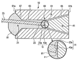
- the optical device 10 includes a light guide member such as an optical fiber 21 that guides light, an optical element 41 that functions by being irradiated with light guided by the optical fiber 21, and A holding member 61 that directly holds the optical fiber 21 and the optical element 41 is provided.
- the optical fiber 21 is disposed at one end 23 of the optical fiber 21 and has a planar emission end face 23 a that emits light. This light is, for example, laser light.
- the other end 25 side of the optical fiber 21 is covered with a coating layer (not shown) made of, for example, resin that protects the optical fiber 21.
- the optical fiber 21 is formed of at least one of glass and plastic, for example.
- the diameter of the optical fiber 21 is, for example, 0.125 mm.
- An optical element 41 as shown in FIG. 1 has a phosphor, for example.
- the optical element 41 emits light such as fluorescent light to the outside by being irradiated with the light guided by the optical fiber 21.
- the optical element 41 has, for example, a truncated cone shape.
- the optical element 41 is not limited to having a truncated cone shape, and may have a cylindrical shape, a hemispherical shape, or a parabolic shape.
- the rigidity of the optical element 41 is larger than the rigidity of the optical fiber 21.
- the optical element 41 has, for example, a planar end face 43a.
- the one end face 43a functions as an incident end face on which light emitted from the emission end face 23a is incident.
- the one end face 43a abuts the emission end face 23a optically and mechanically so that the optical fiber 21 and the optical element 41 are optically coupled.
- the one end face 43a is larger than the emission end face 23a.
- the holding member 61 as shown in FIG. 1 has a ferrule formed of, for example, at least one of zirconia, glass, and metal. This metal is made of, for example, at least one of nickel, SUS, and brass.
- the holding member 61 has, for example, a cylindrical shape. The outer diameter of the holding member 61 is, for example, 1.0 mm.
- the holding member 61 includes a first accommodating portion 63 that accommodates the one end portion 23 of the optical fiber 21 and a second accommodating portion 65 that accommodates the optical element 41. Has inside.
- the holding member 61 includes the optical fiber 21 and the optical element 41 by the first housing portion 63 and the second housing portion 65 so that the optical fiber 21 and the optical element 41 are optically coupled inside the holding member 61. Is held directly inside the holding member 61.
- the holding member 61 directly holds the optical fiber 21 without using a member in the first housing portion 63, and directly holds the optical element 41 without using a member in the second housing portion 65.
- the optical fiber 21 accommodated in the first accommodating portion 63 and the optical element 41 accommodated in the second accommodating portion 65 are in direct contact with each other inside the holding member 61. More specifically, only the exit end face 23a of the optical fiber 21 and the one end face 43a of the optical element 41 are in optical and mechanical contact so as to be optically coupled to each other.
- the first accommodating portion 63 and the second accommodating portion 65 are configured so that the light emitted from the emission end face 23 a of the optical fiber 21 enters the one end face 43 a of the optical element 41.
- they communicate with each other inside the holding member 61.
- the first housing portion 63 and the second housing portion 65 communicate with each other in the axial direction of the holding member 61, for example, at the center of gravity of the holding member 61.
- the central axis of the first housing part 63 and the central axis of the second housing part 65 are coaxial so that the light emitted from the emission end face 23a of the optical fiber 21 enters the one end face 43a of the optical element 41. It is arranged.
- the 1st accommodating part 63 and the 2nd accommodating part 65 are arrange
- the first housing portion 63 is disposed on the one end surface 61 a side of the holding member 61
- the second housing portion 65 is disposed on the other end surface 61 b side of the holding member 61.
- the first accommodating portion 63 is provided for the holding member 61 to hold the optical fiber 21 and functions as a holding hole for holding the optical fiber 21.
- the first housing portion 63 functions as an insertion hole for inserting the optical fiber 21 into the holding member 61.
- the first housing portion 63 is larger than the optical fiber 21 so that the first housing portion 63 has a size that allows deformation and movement of the optical fiber 21. Is also big. That is, the optical fiber 21 accommodated in the first accommodating portion 63 can be bent, deformed, and moved inside the first accommodating portion 63, and the emission end face 23a follows the one end face 43a so that the entire emission end face 23a is integrated.
- the first accommodating portion 63 is formed to be slightly larger than the optical fiber 21 so as to come into surface contact with the end surface 43a.
- the first accommodating portion 63 has, for example, a cylindrical shape.
- the diameter of the 1st accommodating part 63 is 0.13 mm, for example.
- the holding member 61 has a thickness of, for example, 0.87 mm.
- the holding member 61 guides the one end portion 23 of the optical fiber 21 to the first accommodating portion 63 so that the optical fiber 21 is accommodated in the first accommodating portion 63.
- the guide port 67 is disposed on the one end surface 61 a of the holding member 61.
- the guide port 67 communicates with the outside of the optical device 10 and the first housing portion 63.
- the guide port 67 has a truncated cone shape whose diameter is reduced from the one end surface 61 a of the holding member 61 toward the other end surface 61 b of the holding member 61, and is a tapered taper.
- the above-described coating layer (not shown) is disposed only on the one end surface 61 a side of the holding member 61, specifically, near the guide port 67, and is not inserted into the first housing portion 63. For this reason, the one end part 23 of the optical fiber 21 is exposed from the coating layer.
- the second accommodating portion 65 is disposed so that the holding member 61 holds the optical element 41, and functions as a holding hole.
- the second accommodating portion 65 functions as an insertion hole for inserting the optical element 41 into the holding member 61.
- the second accommodating portion 65 has the same shape as the optical element 41, for example, a truncated cone shape. Therefore, the second accommodating portion 65 is reduced in diameter from the other end surface 61b toward the one end surface 61a.
- the second accommodating portion 65 has substantially the same size as the optical element 41 and has a size such that the optical element 41 adheres to the second accommodating portion 65.
- the second accommodating portion 65 may have a size that allows the optical element 41 to fit into the second accommodating portion 65.
- the second accommodating portion 65 penetrates the other end surface 61 b of the holding member 61 in the axial direction of the holding member 61.
- the optical device 10 further includes a refractive index adjusting material 81 disposed at least in the optical coupling portion 11 formed to optically couple the optical fiber 21 and the optical element 41.
- the optical coupling unit 11 includes, for example, an emission end face 23a, one end face 43a, and between the emission end face 23a and the one end face 43a in the axial direction of the holding member 61.
- the refractive index adjusting material 81 is applied to, for example, the emission end face 23a and the one end face 43a, and is interposed between the emission end face 23a and the one end face 43a in the axial direction of the holding member 61.
- the refractive index adjusting material 81 is not limited to this, and may be filled with a communication portion 69 in which the first storage portion 63 and the second storage portion 65 communicate with each other.
- the refractive index adjusting material 81 is bonded to the optical fiber 21, the optical element 41, and the inner peripheral surface of the holding member 61, and also functions as an adhesive that bonds the optical fiber 21 and the optical element 41 to the holding member 61.
- the refractive index adjusting member 81 is filled in at least a part of the first accommodating portion 63 and at least a part of the guide port 67 in order to bond the optical fiber 21 including the coating layer to the holding member 61.
- the refractive index adjusting material 81 is filled in at least a part of the second accommodating portion 65 in order to adhere the optical element 41 to the holding member 61.
- the refractive index adjusting material 81 is filled in a defoamed state.
- Such a refractive index adjusting material 81 is, for example, any one of an optical adhesive, silicone oil, silicone adhesive, silicone resin, and epoxy.
- the refractive index adjusting material 81 is an adhesive that hardens when heated in a high-temperature tank, for example.
- the refractive index adjusting material 81 is bonded to the optical fiber 21, the optical element 41, and the inner peripheral surface of the holding member 61 by curing, and bonds the optical fiber 21 and the optical element 41 to the holding member 61.
- the cured refractive index adjusting material 81 is bonded to the optical fiber 21, the optical element 41, and the inner peripheral surface of the holding member 61, so that the optical fiber 21, the optical element 41, and the holding member 61 are integrated.
- the cured refractive index adjusting material 81 is formed as a rigidity improving member that improves the rigidity of the optical device 10.
- the refractive index adjusting material 81 adjusts the refractive index in the optical coupling portion 11 as desired. For this reason, the refractive index adjusting material 81 has a refractive index higher than the refractive index of air. Further, the refractive index adjusting material 81 further has light resistance. Such a refractive index adjusting material 81 is disposed in order to improve the optical coupling efficiency between the optical fiber 21 and the optical element 41 and to obtain desired optical characteristics.
- the refractive index adjusting material 81 is filled in, for example, the first housing portion 63 and the second housing portion 65 in a defoamed state.
- the refractive index adjusting material 81 is, for example, the first storage portion 63, specifically, the second storage portion 65 while applying pressure with a dispenser so as not to leak after overflowing from the one end surface 61 a side of the holding member 61.
- the liquid is injected from the other end surface 61 b of the holding member 61 into the holding member 61.
- the optical element 41 is inserted into the second housing portion 65 from the other end surface 61b side of the holding member 61 so as to come into contact with the inner peripheral surface of the holding member 61 in the second housing portion 65, and the second housing portion. 65. Since the optical element 41 has substantially the same size as the second housing portion 65, the optical element 41 is positioned with high accuracy in the second housing portion 65.
- the optical fiber 21 is guided to the first housing portion 63 by the guide port 67. Then, the optical fiber 21 is inserted into the first accommodating portion 63 from the guide port 67 so that only the emission end surface 23 a contacts the one end surface 43 a and is accommodated in the first accommodating portion 63.
- first accommodation portion 63 and the second accommodation portion 65 are disposed on the central axis of the holding member 61, for example.
- the optical fiber 21 and the optical element 41 are disposed on the central axis of the holding member 61.
- the holding member 61 is The optical fiber 21 is directly held in the first housing part 63 without any member. Therefore, a part of the emission end face 23a always comes into direct contact with the one end face 43a. At this time, an opening angle ⁇ 1 is formed between the emission end face 23a and the one end face 43a.
- a member (not shown) is held so as to cover the optical fiber 21 as in Patent Document 1 described above, and the optical fiber 21 is attached to the central axis of the first accommodating portion 63 together with a member (not shown).
- the holding member 61 indirectly holds the optical fiber 21 via the member (not shown) in the first housing portion 63.
- the 1st accommodating part 63 shall be very small rather than the member which is not shown in figure.
- the end surface of a member (not shown) is in contact with the one end surface 43a while being inclined with respect to the one end surface 43a. Therefore, the output end face 23a and the one end face 43a are separated from each other, and an opening angle ⁇ 2 (not shown) is formed between the output end face 23a and the one end face 43a.
- the distance between the emission end face 23a and the one end face 43a is shorter than the distance when a member (not shown) is provided. Thereby, the optical coupling efficiency between the optical fiber 21 and the optical element 41 is improved, and desired optical characteristics are obtained.
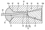
- the first accommodating portion 63 communicates with the second accommodating portion 65 inside the holding member 61, is slightly larger than the optical fiber 21, and accommodates only the optical fiber 21 as a member. Yes. Therefore, as shown in FIG. 2A, even if the optical fiber 21 is inserted into the first housing portion 63 while being skewed with respect to the central axis of the first housing portion 63, the entire emission end surface 23a is the one end surface 43a. It is possible to adjust the inclination of the optical fiber 21 so as to come into surface contact with each other (see FIG. 1). Thus, the optical fiber 21 is positioned with high accuracy.
- the member (not shown) including the optical fiber 21 is bent so that the opening angle ⁇ 2 is 0 or smaller than the opening angle ⁇ 1.
- the 1st accommodating part 63 is slightly larger than the optical fiber 21, and accommodates only the optical fiber 21 as a member.
- the first housing portion 63 has a size that allows deformation and movement of the optical fiber 21. Therefore, as shown in FIG.
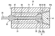
- the optical fiber 21 is When inserted into the first accommodating portion 63, only the emission end face 23a comes into contact with the one end face 43a, so that the optical fiber 21 having a lower rigidity than the optical element 41 is bent as shown in FIG. 2B. At this time, the optical fiber 21 bends so that the output end face 23a follows the one end face 43a. As a result, as shown in FIG. 2B, the entire emission end face 23a comes into surface contact with the one end face 43a. As a result, the optical fiber 21 is positioned with high accuracy, the optical coupling efficiency between the optical fiber 21 and the optical element 41 is improved, and desired optical characteristics are obtained.
- the holding member 61 is inserted into the high temperature bath and heated. Thereby, the refractive index adjusting material 81 is cured. Therefore, the optical fiber 21 and the optical element 41 are bonded to the inner peripheral surface of the holding member 61 and held by the holding member 61 in a state where the emission end face 23 a is in contact with the one end face 43 a. Thereby, the optical device 10 is assembled.
- the first accommodation portion 63 and the second accommodation portion 65 communicate with each other inside the holding member 61, and the optical fiber 21 accommodated in the first accommodation portion 63 and the second accommodation portion 63. Only the optical element 41 accommodated in the accommodating portion 65 is in direct contact with each other inside the holding member 61. Thereby, in this embodiment, the distance between the optical fiber 21 and the optical element 41 can be reduced, the optical fiber 21 and the optical element 41 can be positioned with high accuracy, and the optical coupling efficiency between the optical fiber 21 and the optical element 41 is improved. And desired optical characteristics can be obtained.
- the holding member 61 directly holds the optical fiber 21 in the first housing portion 63 without using any member. Therefore, in this embodiment, as shown in FIG. 2A, even if the optical fiber 21 is skewed with respect to the central axis of the first housing portion 63 and inserted into the first housing portion 63, the emission end face 23a and The one end face 43a can be brought into contact with each other. At this time, in this embodiment, the distance between the emission end face 23a and the one end face 43a can be made shorter than the distance when a member (not shown) is provided. Therefore, in this embodiment, the optical coupling efficiency between the optical fiber 21 and the optical element 41 can be improved, and desired optical characteristics can be obtained.
- the first accommodating portion 63 communicates with the second accommodating portion 65 inside the holding member 61, is slightly larger than the optical fiber 21, and accommodates only the optical fiber 21 as a member. Yes. Therefore, in this embodiment, as shown in FIG. 2A, even if the optical fiber 21 is skewed with respect to the central axis of the first housing portion 63 and inserted into the first housing portion 63, the entire emission end face 23 a Can adjust the inclination of the optical fiber 21 so as to be in surface contact with the one end face 43a (see FIG. 1). Thus, in this embodiment, the optical fiber 21 can be positioned with high accuracy.
- the 1st accommodating part 63 is slightly larger than the optical fiber 21, and accommodates only the optical fiber 21 as a member.
- the first housing portion 63 has a size that allows deformation and movement of the optical fiber 21. Therefore, in this embodiment, as shown in FIG. 2B, even if the optical element 41 is accommodated with a slight inclination with respect to the central axis of the holding member 61, and the one end surface 43 a is inclined with respect to the central axis of the holding member 61.
- the optical fiber 21 having a lower rigidity than the optical element 41 can be bent by the output end face 23a coming into contact with the one end face 43a.
- the optical fiber 21 bends so that the output end face 23a follows the one end face 43a. Thereby, in this embodiment, the whole emission end surface 23a can be in surface contact with the one end surface 43a. Therefore, in this embodiment, the optical fiber 21 can be positioned with high accuracy, the optical coupling efficiency between the optical fiber 21 and the optical element 41 can be improved, and desired optical characteristics can be obtained.
- the holding member 61 indirectly holds the optical fiber 21 via a member (not shown), the optical fiber 21 and the member (not shown) are housed in the first housing portion 63, and the member (not shown) can tilt.
- the first accommodating portion 63 needs to be large. Thereby, the thickness of the holding member 61 in the periphery of the first accommodating portion 63 becomes thinner than that in the present embodiment.
- the holding member 61 directly holds the optical fiber 21 and only the optical fiber 21 is accommodated in the first accommodating portion 63. Therefore, in the present embodiment, the thickness of the holding member 61 in the periphery of the first accommodating portion 63 can be increased compared to the case where a member (not shown) is provided, and the holding member 61 is missing or cracked. Can be prevented. And in this embodiment, the intensity
- the holding member 61 directly holds the optical fiber 21, heat generated from the optical fiber 21 can be directly transmitted to the holding member 61, and heat dissipation can be improved.
- the optical axis 21 and the optical element 41 can be easily and accurately arranged by coaxially arranging the central axis of the first accommodating part 63 and the central axis of the second accommodating part 65.
- the optical fiber 21 and the optical element 41 can be reliably optically coupled.
- the refractive index adjusting material 81 can improve the optical coupling efficiency between the optical fiber 21 and the optical element 41 and obtain desired optical characteristics.
- the optical fiber 21 and the optical element 41 can be bonded to the holding member 61 by the refractive index adjusting material 81, and the optical fiber 21 and the optical element 41 can be easily positioned.
- the inclination of only the optical fiber 21 is adjusted, and only the optical fiber 21 is bent.
- the positional shift and optical loss at the time of optical coupling can be suppressed.
- the optical coupling portion 11 formed for optically coupling the optical fiber 21 and the optical element 41 communicates with the outside of the holding member 61, and the communication disposed inside the holding member 61.
- a portion 71 is further provided.
- the communication unit 71 functions as a discharge unit that discharges the bubbles that have escaped from the refractive index adjusting material 81 in the optical coupling unit 11 to the outside of the holding member 61.
- the communication portion 71 is disposed along the radial direction of the holding member 61.
- two communicating portions 71 are disposed, for example, and one communicating portion 71 and the other communicating portion 71 are disposed 180 degrees apart from each other in the circumferential direction of the holding member 61. Yes.
- the communication portion 71 is disposed up to the one end face 43a side along the axial direction of the holding member 61, and the holding member 61 has a lower portion than the first accommodating portion 63. Disposed in the radial direction. In this case, the diameter of the first accommodating portion 63 is increased, for example, toward the one end face 43a so as to communicate with the communicating portion 71 in the optical coupling portion 11.
- the communication part 71 can reliably discharge the bubbles that have escaped from the refractive index adjusting material 81 to the outside of the holding member 61. Therefore, in this modification, it can prevent reliably that a bubble mixes in the optical coupling part 11, can prevent that optical coupling efficiency falls with a bubble, and can obtain a desired optical characteristic reliably.
- the number, shape, and size of the communication portions 71 are not particularly limited.
- the first accommodating portion 63 is formed to be tapered so as to become thinner toward the second accommodating portion 65 in the axial direction of the holding member 61.
- the first accommodating portion 63 has a truncated cone shape that is reduced in diameter toward the second accommodating portion 65, for example.
- the 1st accommodating part 63 has a taper shape.
- the diameter on the one end face 61 a side is larger than the diameter of the optical fiber 21.
- the first accommodating portion 63 also serves as the guide port 67.
- the optical fiber 21 can be easily inserted into the first accommodating portion 63 by the first accommodating portion 63 formed in a tapered shape, and the optical fiber 21 can be positioned with higher accuracy.
- the gap between the optical fiber 21 and the inner peripheral surface of the holding member 61 in the first accommodating portion 63 is formed larger on the one end surface 61a side than in the first embodiment. . Therefore, when the optical fiber 21 is accommodated in the first accommodating part 63 after the refractive index adjusting material 81 is filled in the first accommodating part 63, in this embodiment, the optical fiber 21 is replaced with the first accommodating part 63.
- the optical fiber 21 can be positioned freely.
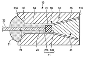
- the optical device 10 further includes an elastic member 91 that is disposed in the optical coupling portion 11 formed to optically couple the optical fiber 21 and the optical element 41 and has a rigidity lower than that of the optical fiber 21.
- the elastic member 91 is interposed between the emission end surface 23 a of the optical fiber 21 and the one end surface 43 a of the optical element 41 in the axial direction of the holding member 61.
- the elastic member 91 prevents the emission end face 23a and the one end face 43a from being damaged when the emission end face 23a of the optical fiber 21 and the one end face 43a of the optical element 41 come into contact with each other, and cushions an impact at the time of contact. Functions as a cushioning material.
- the elastic member 91 is, for example, rubber formed of silicon resin.
- the elastic member 91 is disposed in advance on either the emission end face 23a or the one end face 43a.
- the elastic member 91 is housed in the first housing portion 63 together with the optical fiber 21, as shown in FIG.
- the elastic member 91 is accommodated in the second accommodating portion 65 together with the optical element 41.
- the elastic member 91 only needs to be disposed in at least one of the first housing portion 63 and the second housing portion 65.
- the emitting end surface 23a of the optical fiber 21 and the one end surface 43a of the optical element 41 are in contact with each other by the elastic member 91, the emitting end surface 23a and the one end surface 43a can be prevented from being damaged. Shock can be buffered when touching.
- the elastic member 91 has a higher transmittance than the transmittance of air. Therefore, in this embodiment, even if the elastic member 91 is interposed between the emission end surface 23a and the one end surface 43a, the optical coupling efficiency can be prevented from being lowered by the elastic member 91, and desired optical characteristics can be obtained. it can.
- the present invention is not limited to the above-described embodiment as it is, and can be embodied by modifying the constituent elements without departing from the scope of the invention in the implementation stage. Further, various inventions can be formed by appropriately combining a plurality of constituent elements disclosed in the embodiment.
Landscapes
- Physics & Mathematics (AREA)
- General Physics & Mathematics (AREA)
- Optics & Photonics (AREA)
- Optical Couplings Of Light Guides (AREA)
- Light Guides In General And Applications Therefor (AREA)
- Optical Fibers, Optical Fiber Cores, And Optical Fiber Bundles (AREA)
Abstract
光学デバイス10は、光を導光する、例えば光ファイバ21などの導光部材と、前記光ファイバによって導光された光が照射されることで機能する、例えば蛍光体を有する光学素子41と、保持部材61とを有している。前記保持部材は、前記光ファイバの一端部23を収容する第1の収容部63と、前記光学素子を収容する第2の収容部65とを、前記保持部材の内部に有している。前記保持部材は、前記第1の収容部と前記第2の収容部とによって前記光ファイバと前記光学素子とを前記保持部材の内部で直接保持している。前記第1の収容部と前記第2の収容部とは、前記保持部材の内部にて連通している。前記第1の収容部に収容される前記光ファイバと、前記第2の収容部に収容される前記光学素子とは、前記保持部材の内部にて互いに直接当接している。前記第1の収容部は、前記第1の収容部が前記光ファイバの変形及び移動を許容する大きさを有するように、前記光ファイバよりも大きい。
Description
本発明は、導光部材と光学素子とを有する光学デバイスに関する。
例えば特許文献1は、キャップと光変換部材とを有する光部品を開示している。
キャップは、フェルールが嵌合する第1の孔を有する嵌合部と、第1の孔に通じる第2の孔を有する配置部とを有している。フェルールは、導光部材である光ファイバがフェルールを挿通するように、光ファイバを保持している。
光変換部材は、第2の孔に配設されている。光変換部材は、光変換部材と嵌合部との間に配設された低融点ガラスまたは樹脂によって固定されている。
キャップは、フェルールが嵌合する第1の孔を有する嵌合部と、第1の孔に通じる第2の孔を有する配置部とを有している。フェルールは、導光部材である光ファイバがフェルールを挿通するように、光ファイバを保持している。
光変換部材は、第2の孔に配設されている。光変換部材は、光変換部材と嵌合部との間に配設された低融点ガラスまたは樹脂によって固定されている。
なおフェルールが第1の孔と嵌合し、フェルールの側面の少なくとも一部が第1の孔の内周面にYAG溶接されることにより、キャップはフェルールに固定されている。またキャップの端部がフェルールと固定することもできる。
また、接着剤と抵抗溶接と圧入とかしめとのいずれかによって、キャップはフェルールに固定することも可能である。
特許文献1において、光ファイバがフェルールに接着固定した後に、光ファイバの端面とフェルールの端面とが同一平面上に配設されるように、光ファイバの端面とフェルールの端面とが研磨される。そしてフェルールはキャップに固定されている光変換部材に突き当たることで、光ファイバと光変換部材とが位置あわせされている。
しかしながら、この位置あわせにおいて、フェルールの端面と光変換部材の端面とが平行に配設されることは困難である。よってほとんどの場合、フェルールの端面は光変換部材の端面に対して傾いてしまい、フェルールの端面と光学部材の端面とが完全に突き当たることは困難である。従って、フェルールの一部分のみが光変換部材に突き当たり、光ファイバと光変換部材との間には隙間が生じる。
例えば空気がこの隙間に介在すると、光ファイバを導光した光は隙間において反射し、光は光変換部材に入射しない。このように光ファイバと光変換部材とが高精度に位置決めされないと、光の損失が生じる。
この点を解消するために、例えば屈折率整合材が隙間に充填される。しかしこの場合、光ファイバの端面が光変換部材の端面に対して傾いるため、光ファイバの端面から出射される光は光変換部材の所望の位置から光変換部材に入射せず、所望の光学特性を得られない。
このように、導光部材と光学素子とが高精度に位置決めされないと、所望の光学特性が得られない。
本発明は、これらの事情に鑑みてなされたものであり、導光部材と光学素子とが高精度に位置決めされ、所望の光学特性を得られる光学デバイスを提供することを目的とする。
本発明の光源デバイスの一態様は、光を導光する導光部材と、前記導光部材によって導光された前記光を照射されることで機能する光学素子と、前記導光部材を収容する第1の収容部と、前記光学素子を収容する第2の収容部とを内部に有し、前記導光部材と前記光学素子とが内部で光結合するように、前記第1の収容部と前記第2の収容部とによって前記導光部材と前記光学素子とを内部で保持している保持部材と、を具備し、前記第1の収容部と前記第2の収容部とは、前記保持部材の内部にて連通し、前記第1の収容部に収容される前記導光部材と、前記第2の収容部に収容される前記光学素子とは、前記保持部材の内部にて互いに当接している。
本発明によれば、導光部材と光学素子とが高精度に位置決めされ、所望の光学特性を得られる光学デバイスを提供することができる。
以下、図面を参照して本発明の実施形態について詳細に説明する。
[第1の実施形態]
[構成]
図1と図2Aと図2Bとを参照して第1の実施形態について説明する。
[光学デバイス10]
図1に示すように、光学デバイス10は、光を導光する例えば光ファイバ21などの導光部材と、光ファイバ21によって導光された光を照射されることで機能する光学素子41と、光ファイバ21と光学素子41とを直接保持する保持部材61とを有している。
[第1の実施形態]
[構成]
図1と図2Aと図2Bとを参照して第1の実施形態について説明する。
[光学デバイス10]
図1に示すように、光学デバイス10は、光を導光する例えば光ファイバ21などの導光部材と、光ファイバ21によって導光された光を照射されることで機能する光学素子41と、光ファイバ21と光学素子41とを直接保持する保持部材61とを有している。
[光ファイバ21]
図1に示すように、光ファイバ21は、光ファイバ21の一端部23に配設され、光を出射する平面状の出射端面23aを有している。この光は、例えばレーザ光である。光ファイバ21の他端部25側は、光ファイバ21を保護する例えば樹脂製の図示しない被覆層によって覆われている。光ファイバ21は、例えばガラスとプラスチックとの少なくとも一方によって形成されている。光ファイバ21の直径は、例えば0.125mmである。
図1に示すように、光ファイバ21は、光ファイバ21の一端部23に配設され、光を出射する平面状の出射端面23aを有している。この光は、例えばレーザ光である。光ファイバ21の他端部25側は、光ファイバ21を保護する例えば樹脂製の図示しない被覆層によって覆われている。光ファイバ21は、例えばガラスとプラスチックとの少なくとも一方によって形成されている。光ファイバ21の直径は、例えば0.125mmである。
[光学素子41]
図1に示すような光学素子41は、例えば蛍光体を有している。光学素子41は、光ファイバ21によって導光された光を照射されることで、例えば蛍光などの光を外部に出射する。光学素子41は、例えば円錐台形状を有している。なお光学素子41は、円錐台形状を有することに限定することはなく、円柱形状や半球形状や放物形状を有していてもよい。光学素子41の剛性は、光ファイバ21の剛性よりも大きい。光学素子41は、例えば平面状の一端面43aを有している。一端面43aは、出射端面23aから出射された光が入射する入射端面として機能する。この一端面43aは、光ファイバ21と光学素子41とが光結合するために、出射端面23aと光学的及び機械的に当接する。一端面43aは、出射端面23aよりも大きい。
図1に示すような光学素子41は、例えば蛍光体を有している。光学素子41は、光ファイバ21によって導光された光を照射されることで、例えば蛍光などの光を外部に出射する。光学素子41は、例えば円錐台形状を有している。なお光学素子41は、円錐台形状を有することに限定することはなく、円柱形状や半球形状や放物形状を有していてもよい。光学素子41の剛性は、光ファイバ21の剛性よりも大きい。光学素子41は、例えば平面状の一端面43aを有している。一端面43aは、出射端面23aから出射された光が入射する入射端面として機能する。この一端面43aは、光ファイバ21と光学素子41とが光結合するために、出射端面23aと光学的及び機械的に当接する。一端面43aは、出射端面23aよりも大きい。
[保持部材61]
図1に示すような保持部材61は、例えばジルコニアとガラスと金属との少なくとも1つによって形成されているフェルールを有している。この金属は、例えばニッケルとSUSと真鍮との少なくとも1つによって構成されている。保持部材61は、例えば円筒形状を有している。保持部材61の外径は、例えば1.0mmである。
図1に示すような保持部材61は、例えばジルコニアとガラスと金属との少なくとも1つによって形成されているフェルールを有している。この金属は、例えばニッケルとSUSと真鍮との少なくとも1つによって構成されている。保持部材61は、例えば円筒形状を有している。保持部材61の外径は、例えば1.0mmである。
また図1に示すように、保持部材61は、光ファイバ21の一端部23を収容する第1の収容部63と、光学素子41を収容する第2の収容部65とを、保持部材61の内部に有している。そして保持部材61は、光ファイバ21と光学素子41とが保持部材61の内部で光結合するように、第1の収容部63と第2の収容部65とによって光ファイバ21と光学素子41とを保持部材61の内部で直接保持している。このように保持部材61は、第1の収容部63において部材を介さずに光ファイバ21を直接保持し、第2の収容部65において部材を介さずに光学素子41を直接保持している。第1の収容部63に収容される光ファイバ21と、第2の収容部65に収容される光学素子41とは、保持部材61の内部にて互いに直接当接している。より詳細には、光ファイバ21の出射端面23aと、光学素子41の一端面43aとのみが、互いに光結合するように光学的及び機械的に当接している。
図1に示すように、第1の収容部63と第2の収容部65とは、光ファイバ21の出射端面23aから出射した光が光学素子41の一端面43aに入射するように、保持部材61の軸方向において保持部材61の内部にて互いに連通している。詳細には、第1の収容部63と第2の収容部65とは、保持部材61の軸方向において、例えば保持部材61の重心にて、互いに連通している。また第1の収容部63の中心軸と第2の収容部65の中心軸とは、光ファイバ21の出射端面23aから出射した光が光学素子41の一端面43aに入射するように、同軸上に配設されている。このため第1の収容部63と第2の収容部65とは、例えば保持部材61の中心軸上に配設されている。第1の収容部63は保持部材61の一端面61a側に配設され、第2の収容部65は保持部材61の他端面61b側に配設されている。
第1の収容部63は、保持部材61が光ファイバ21を保持するために配設されており、光ファイバ21を保持する保持孔として機能する。また第1の収容部63は、光ファイバ21が保持部材61に挿入される挿入孔として機能する。図1と図2Aと図2Bとに示すように、第1の収容部63は、第1の収容部63が光ファイバ21の変形及び移動を許容する大きさを有するように、光ファイバ21よりも大きい。つまり、第1の収容部63に収容された光ファイバ21が第1の収容部63の内部にて撓み、変形及び移動でき、出射端面23aが一端面43aに追従して出射端面23a全面が一端面43aと面当接するように、第1の収容部63は光ファイバ21よりも微小に大きくなるように形成されている。
第1の収容部63は、例えば円柱形状を有している。第1の収容部63の直径は、例えば0.13mmである。このため、第1の収容部63の径方向において、保持部材61は、例えば0.87mmの肉厚を有することとなる。
なお図1に示すように、保持部材61は、光ファイバ21が第1の収容部63に収容されるように、光ファイバ21の一端部23を第1の収容部63にガイドするガイド口67を有している。ガイド口67は、保持部材61の一端面61aに配設されている。ガイド口67は、光学デバイス10の外部及び第1の収容部63と連通している。ガイド口67は、保持部材61の一端面61aから保持部材61の他端面61b側に向かって縮径している円錐台形状を有しており、傾斜しているテーパとなっている。なお前述した図示しない被覆層は、保持部材61の一端面61a側、詳細にはガイド口67付近にまで配設されているのみであり、第1の収容部63には挿入されない。このため光ファイバ21の一端部23は、被覆層から露出している。
第2の収容部65は、保持部材61が光学素子41を保持するために配設されており、保持孔として機能する。また第2の収容部65は、光学素子41が保持部材61に挿入される挿入孔として機能する。第2の収容部65は、光学素子41と同形状、例えば円錐台形状を有している。よって、第2の収容部65は、他端面61bから一端面61aに向かって縮径している。第2の収容部65は、光学素子41と略同一の大きさ、且つ光学素子41が第2の収容部65と接着する大きさを有している。なお第2の収容部65は、光学素子41が第2の収容部65と嵌合する大きさを有していてもよい。第2の収容部65は、保持部材61の軸方向において、保持部材61の他端面61bを貫通している。
[屈折率調整材81]
また図1に示すように、光学デバイス10は、光ファイバ21と光学素子41とが光結合するために形成される光結合部11に少なくとも配設される屈折率調整材81をさらに有している。この場合、光結合部11は、例えば、出射端面23aと、一端面43aと、保持部材61の軸方向において出射端面23aと一端面43aとの間とを含む。そして屈折率調整材81は、例えば出射端面23aと一端面43aとに塗布され、保持部材61の軸方向において出射端面23aと一端面43aとの間に介在する。なお屈折率調整材81は、これに限定されることは無く、第1の収容部63と第2の収容部65とが互いに連通する連通部分69にて充填されていても良い。
また図1に示すように、光学デバイス10は、光ファイバ21と光学素子41とが光結合するために形成される光結合部11に少なくとも配設される屈折率調整材81をさらに有している。この場合、光結合部11は、例えば、出射端面23aと、一端面43aと、保持部材61の軸方向において出射端面23aと一端面43aとの間とを含む。そして屈折率調整材81は、例えば出射端面23aと一端面43aとに塗布され、保持部材61の軸方向において出射端面23aと一端面43aとの間に介在する。なお屈折率調整材81は、これに限定されることは無く、第1の収容部63と第2の収容部65とが互いに連通する連通部分69にて充填されていても良い。
また屈折率調整材81は、光ファイバ21と光学素子41と保持部材61の内周面とに接着し、光ファイバ21と光学素子41とを保持部材61に接着する接着剤としても機能する。この場合、屈折率調整材81は、被覆層を含む光ファイバ21を保持部材61に接着するために、第1の収容部63の少なくとも一部とガイド口67の少なくとも一部に充填される。また屈折率調整材81は、光学素子41を保持部材61に接着するために、第2の収容部65の少なくとも一部に充填される。
屈折率調整材81は、脱泡された状態で充填される。
屈折率調整材81は、脱泡された状態で充填される。
このような屈折率調整材81は、例えば、光学用の接着剤と、シリコーンオイルと、シリコーン接着剤と、シリコーン樹脂と、エポキシ等の接着剤とのいずれか1つである。
なお屈折率調整材81は、例えば高温槽で加熱されることで硬化する接着剤である。屈折率調整材81は、硬化によって光ファイバ21と光学素子41と保持部材61の内周面とに接着し、光ファイバ21と光学素子41とを保持部材61に接着する。硬化した屈折率調整材81は、光ファイバ21と光学素子41と保持部材61の内周面とに接着することで、光ファイバ21と光学素子41と保持部材61と一体となる。また硬化した屈折率調整材81は、光学デバイス10の剛性を向上させる剛性向上部材として形成される。
また屈折率調整材81は、光結合部11における屈折率を所望に調整する。このため屈折率調整材81は、空気の屈折率よりも高い屈折率を有している。また、屈折率調整材81は、耐光性をさらに有している。このような屈折率調整材81は、光ファイバ21と光学素子41との光結合効率を向上させ、所望の光学特性を得るために配設されている。
[組立方法]
次に図1と図2Aと図2Bとを参照して本実施形態における光学デバイス10の組立方法について説明する。
屈折率調整材81は、脱泡された状態で、例えば第1の収容部63と第2の収容部65とに充填される。このとき屈折率調整材81は、例えば、第1の収容部63、詳細には保持部材61の一端面61a側から溢れてから漏れないように、ディスペンサで圧力をかけながら第2の収容部65、詳細には保持部材61の他端面61bから保持部材61の内部に注入される。
次に図1と図2Aと図2Bとを参照して本実施形態における光学デバイス10の組立方法について説明する。
屈折率調整材81は、脱泡された状態で、例えば第1の収容部63と第2の収容部65とに充填される。このとき屈折率調整材81は、例えば、第1の収容部63、詳細には保持部材61の一端面61a側から溢れてから漏れないように、ディスペンサで圧力をかけながら第2の収容部65、詳細には保持部材61の他端面61bから保持部材61の内部に注入される。
光学素子41は、第2の収容部65における保持部材61の内周面と当接するように、保持部材61の他端面61b側から第2の収容部65に挿入されて、第2の収容部65に収容される。光学素子41は、第2の収容部65と略同一の大きさを有しているため、第2の収容部65に高精度に位置決めされる。
光ファイバ21は、ガイド口67によって第1の収容部63にガイドされる。そして光ファイバ21は、出射端面23aのみが一端面43aと当接するように、ガイド口67から第1の収容部63に挿入されて、第1の収容部63に収容される。
なお第1の収容部63と第2の収容部65とは例えば保持部材61の中心軸上に配設されている。このため、光ファイバ21と光学素子41とは保持部材61の中心軸上に配設される。
なお図2Aに示すように、本実施形態では、光ファイバ21が第1の収容部63の中心軸に対して斜行して第1の収容部63に挿入されたとしても、保持部材61は第1の収容部63において部材を介さずに光ファイバ21を直接保持している。よって出射端面23aの一部は一端面43aと必ず直接当接する。このとき出射端面23aと一端面43aとの間に開き角度をθ1が形成される。
ここで本実施形態とは異なり、例えば前述した特許文献1のように図示しない部材が光ファイバ21を覆うように保持し、光ファイバ21が図示しない部材と共に第1の収容部63の中心軸に対して斜行して第1の収容部63に挿入されたとする。つまり保持部材61は、第1の収容部63において、この図示しない部材を介して光ファイバ21を間接的に保持したとする。この場合、第1の収容部63は、図示しない部材よりも極微小に大きいとする。またこの場合、図示しない部材の端面は、一端面43aに対して傾斜した状態で、一端面43aと当接する。よって、出射端面23aと一端面43aとは離れ、出射端面23aと一端面43aとの間に開き角度をθ2(不図示)が形成される。
そして図1に示す開き角度θ1は、図示しない開き角度θ2よりも図示しない部材の厚み分だけ小さくなる。よって、出射端面23aと一端面43aとの距離は、図示しない部材が配設されている場合の距離に比べて短くなる。これにより、光ファイバ21と光学素子41との光結合効率は向上し、所望の光学特性が得られる。
また開き角度θ2が0または開き角度θ1よりも小さくなるように、図示しない部材を含む光ファイバ21の傾きを調整することは、図示しない部材と第1の収容部63との間の極微小な隙間との関係によって容易ではない。
しかしながら本実施形態では、第1の収容部63は、第2の収容部65と保持部材61の内部にて連通し、光ファイバ21よりも微小に大きく、部材として光ファイバ21のみを収容している。このため図2Aに示すように、光ファイバ21が第1の収容部63の中心軸に対して斜行して第1の収容部63に挿入されたとしても、出射端面23a全面が一端面43aと面当接するように(図1参照)、光ファイバ21の傾きの調整は可能である。このように光ファイバ21は、高精度に位置決めされる。
しかしながら本実施形態では、第1の収容部63は、第2の収容部65と保持部材61の内部にて連通し、光ファイバ21よりも微小に大きく、部材として光ファイバ21のみを収容している。このため図2Aに示すように、光ファイバ21が第1の収容部63の中心軸に対して斜行して第1の収容部63に挿入されたとしても、出射端面23a全面が一端面43aと面当接するように(図1参照)、光ファイバ21の傾きの調整は可能である。このように光ファイバ21は、高精度に位置決めされる。
また前述した図示しない部材が光ファイバ21を保持している場合、開き角度をθ2が0または開き角度θ1よりも小さくなるように、光ファイバ21を含む図示しない部材が撓むことは、図示しない部材の剛性と、図示しない部材と第1の収容部63との間の極微小な隙間との関係によって容易ではない。
しかしながら本実施形態では、第1の収容部63は、光ファイバ21よりも微小に大きく、部材として光ファイバ21のみを収容している。また第1の収容部63は、光ファイバ21の変形及び移動を許容する大きさを有している。よって図2Aに示すように、光学素子41が保持部材61の中心軸に対して微小に傾いて収容され、一端面43aが保持部材61の中心軸に対して傾いたとしても、光ファイバ21が第1の収容部63に挿入された際、出射端面23aのみが一端面43aと当接することで、図2Bに示すように光学素子41よりも剛性が低い光ファイバ21は撓む。このとき、出射端面23aが一端面43aに追従するように、光ファイバ21は撓む。これにより、図2Bに示すように、出射端面23a全面は、一端面43aと面当接する。結果として、光ファイバ21は高精度に位置決めされ、光ファイバ21と光学素子41との光結合効率は向上し、所望の光学特性が得られる。
しかしながら本実施形態では、第1の収容部63は、光ファイバ21よりも微小に大きく、部材として光ファイバ21のみを収容している。また第1の収容部63は、光ファイバ21の変形及び移動を許容する大きさを有している。よって図2Aに示すように、光学素子41が保持部材61の中心軸に対して微小に傾いて収容され、一端面43aが保持部材61の中心軸に対して傾いたとしても、光ファイバ21が第1の収容部63に挿入された際、出射端面23aのみが一端面43aと当接することで、図2Bに示すように光学素子41よりも剛性が低い光ファイバ21は撓む。このとき、出射端面23aが一端面43aに追従するように、光ファイバ21は撓む。これにより、図2Bに示すように、出射端面23a全面は、一端面43aと面当接する。結果として、光ファイバ21は高精度に位置決めされ、光ファイバ21と光学素子41との光結合効率は向上し、所望の光学特性が得られる。
このような状態で、保持部材61は、高温槽に挿入され加熱される。これにより屈折率調整材81は、硬化する。よって、光ファイバ21と光学素子41とは、出射端面23aが一端面43aと当接した状態で、保持部材61の内周面に接着し、保持部材61によって保持される。
これにより、光学デバイス10が組み立てられる。
これにより、光学デバイス10が組み立てられる。
[効果]
このように本実施形態では、第1の収容部63と第2の収容部65とが保持部材61の内部にて連通し、第1の収容部63に収容される光ファイバ21と第2の収容部65に収容される光学素子41とのみが保持部材61の内部にて直接互いに当接している。これにより本実施形態では、光ファイバ21と光学素子41との間の距離を低減でき、光ファイバ21と光学素子41とを高精度に位置決めでき、光ファイバ21と光学素子41との光結合効率を向上でき、所望の光学特性を得ることができる。
このように本実施形態では、第1の収容部63と第2の収容部65とが保持部材61の内部にて連通し、第1の収容部63に収容される光ファイバ21と第2の収容部65に収容される光学素子41とのみが保持部材61の内部にて直接互いに当接している。これにより本実施形態では、光ファイバ21と光学素子41との間の距離を低減でき、光ファイバ21と光学素子41とを高精度に位置決めでき、光ファイバ21と光学素子41との光結合効率を向上でき、所望の光学特性を得ることができる。
また本実施形態は、保持部材61は第1の収容部63において部材を介さずに光ファイバ21を直接保持している。よって本実施形態では、図2Aに示すように、光ファイバ21が第1の収容部63の中心軸に対して斜行して第1の収容部63に挿入されたとしても、出射端面23aと一端面43aとを互いに当接させることができる。またこのとき、本実施形態では、出射端面23aと一端面43aとの距離を、図示しない部材が配設されている場合の距離に比べて短くできる。よって本実施形態では、光ファイバ21と光学素子41との光結合効率を向上でき、所望の光学特性を得ることができる。
また本実施形態では、第1の収容部63は、第2の収容部65と保持部材61の内部にて連通し、光ファイバ21よりも微小に大きく、部材として光ファイバ21のみを収容している。
よって本実施形態では、図2Aに示すように、光ファイバ21が第1の収容部63の中心軸に対して斜行して第1の収容部63に挿入されたとしても、出射端面23a全面が一端面43aと面当接するように(図1参照)、光ファイバ21の傾きを調整できる。このように本実施形態では、光ファイバ21を高精度に位置決めできる。
よって本実施形態では、図2Aに示すように、光ファイバ21が第1の収容部63の中心軸に対して斜行して第1の収容部63に挿入されたとしても、出射端面23a全面が一端面43aと面当接するように(図1参照)、光ファイバ21の傾きを調整できる。このように本実施形態では、光ファイバ21を高精度に位置決めできる。
また本実施形態では、第1の収容部63は、光ファイバ21よりも微小に大きく、部材として光ファイバ21のみを収容している。また第1の収容部63は、光ファイバ21の変形及び移動を許容する大きさを有している。
よって本実施形態では、図2Bに示すように、光学素子41が保持部材61の中心軸に対して微小に傾いて収容され、一端面43aが保持部材61の中心軸に対して傾いたとしても、光ファイバ21が第1の収容部63に挿入された際、出射端面23aが一端面43aと当接することで、光学素子41よりも剛性が低い光ファイバ21は撓むことができる。このとき、出射端面23aが一端面43aに追従するように、光ファイバ21は撓む。これにより本実施形態では、出射端面23a全面は一端面43aと面当接することができる。よって本実施形態では、光ファイバ21を高精度に位置決めでき、光ファイバ21と光学素子41との光結合効率を向上でき、所望の光学特性を得ることができる。
よって本実施形態では、図2Bに示すように、光学素子41が保持部材61の中心軸に対して微小に傾いて収容され、一端面43aが保持部材61の中心軸に対して傾いたとしても、光ファイバ21が第1の収容部63に挿入された際、出射端面23aが一端面43aと当接することで、光学素子41よりも剛性が低い光ファイバ21は撓むことができる。このとき、出射端面23aが一端面43aに追従するように、光ファイバ21は撓む。これにより本実施形態では、出射端面23a全面は一端面43aと面当接することができる。よって本実施形態では、光ファイバ21を高精度に位置決めでき、光ファイバ21と光学素子41との光結合効率を向上でき、所望の光学特性を得ることができる。
例えば、保持部材61が図示しない部材を介して光ファイバ21を間接的に保持し、光ファイバ21と図示しない部材とが第1の収容部63に収容され、図示しない部材が傾くことができる場合、第1の収容部63は大きくなる必要がある。これにより第1の収容部63の周辺における保持部材61の肉厚が、本実施形態に比べて薄くなる。しかしながら本実施形態では、保持部材61が光ファイバ21を直接保持し、光ファイバ21のみが第1の収容部63に収容される。よって本実施形態では、図示しない部材が配設されている場合に比べて、第1の収容部63の周辺における保持部材61の肉厚を厚くすることができ、保持部材61が欠けることや割れることを防止できる。そして本実施形態では、光学デバイス10の強度を向上でき、部品加工の歩留まりを向上できる。
また本実施形態では、保持部材61が光ファイバ21を直接保持するために、光ファイバ21から生じた熱を保持部材61に直接伝達でき、放熱性を向上できる。
また本実施形態では、第1の収容部63の中心軸と第2の収容部65の中心軸とを同軸上に配設することで、光ファイバ21と光学素子41とを容易且つ高精度に位置決めでき、光ファイバ21と光学素子41とを確実に光結合できる。
また本実施形態では、屈折率調整材81によって、光ファイバ21と光学素子41との光結合効率を向上でき、所望の光学特性を得ることができる。また本実施形態では、屈折率調整材81によって、光ファイバ21と光学素子41とを保持部材61に接着でき、光ファイバ21と光学素子41とを容易に位置決めできる。
また本実施形態では、光ファイバ21のみの傾きを調整し、光ファイバ21のみを撓ませている。これにより本実施形態では、光学素子41の傾きを調整させる場合に比べて、光結合時の位置ずれ及び光学損失を抑えることができる。
[第1の変形例と第2の変形例]
次に図3Aと図3Bとを参照して本実施形態の第1の変形例と第2の変形例とについて説明する。
光学デバイス10は、光ファイバ21と光学素子41とが光結合するために形成される光結合部11と、保持部材61の外部とを連通し、保持部材61の内部に配設されている連通部71をさらに有している。連通部71は、光結合部11における屈折率調整材81から抜けた気泡を保持部材61の外部に排出する排出部として機能する。
次に図3Aと図3Bとを参照して本実施形態の第1の変形例と第2の変形例とについて説明する。
光学デバイス10は、光ファイバ21と光学素子41とが光結合するために形成される光結合部11と、保持部材61の外部とを連通し、保持部材61の内部に配設されている連通部71をさらに有している。連通部71は、光結合部11における屈折率調整材81から抜けた気泡を保持部材61の外部に排出する排出部として機能する。
図3Aに示す第1の変形例において、連通部71は、保持部材61の径方向に沿って配設されている。図3Aに示すように、例えば連通部71は例えば2つ配設されており、一方の連通部71と他方の連通部71とは保持部材61の周方向において互いに180度離れて配設されている。
また図3Bに示す第2の変形例において、連通部71は、保持部材61の軸方向に沿って一端面43a側まで配設されており、第1の収容部63に対して保持部材61の径方向においてずれて配設されている。この場合、第1の収容部63は、光結合部11において連通部71と連通するように、例えば一端面43aに向かって拡径している。
このように本変形例では、連通部71によって、屈折率調整材81から抜けた気泡を保持部材61の外部に確実に排出できる。よって本変形例では、気泡が光結合部11に混入することを確実に防止でき、気泡によって光結合効率が低下することを防止でき、所望の光学特性が確実に得ることができる。
なお連通部71の数と形状と大きさとは、特に限定されない。
なお連通部71の数と形状と大きさとは、特に限定されない。
[第2の実施形態]
次に図4を参照して第2の実施形態について説明する。
第1の収容部63は、保持部材61の軸方向において、第2の収容部65に向かって細くなるように先細に形成されている。第1の収容部63は、例えば第2の収容部65に向かって縮径している円錐台形状を有している。このように第1の収容部63は、テーパ形状を有している。第1の収容部63において、一端面61a側の径の大きさは、光ファイバ21の直径よりも大きい。第1の収容部63は、ガイド口67を兼ねる。
次に図4を参照して第2の実施形態について説明する。
第1の収容部63は、保持部材61の軸方向において、第2の収容部65に向かって細くなるように先細に形成されている。第1の収容部63は、例えば第2の収容部65に向かって縮径している円錐台形状を有している。このように第1の収容部63は、テーパ形状を有している。第1の収容部63において、一端面61a側の径の大きさは、光ファイバ21の直径よりも大きい。第1の収容部63は、ガイド口67を兼ねる。
これにより本実施形態では、先細に形成された第1の収容部63によって、光ファイバ21を第1の収容部63に容易に挿入でき、光ファイバ21をより高精度に位置決めできる。
また本実施形態では、第1の実施形態と比べて、一端面61a側において、光ファイバ21と、第1の収容部63における保持部材61の内周面との間の隙間が大きく形成される。よって屈折率調整材81が第1の収容部63に充填された後に、光ファイバ21が第1の収容部63に収容される場合、本実施形態では、光ファイバ21を第1の収容部63に容易に収容でき、光ファイバ21を自在に位置決めできる。
[第3の実施形態]
次に図5を参照して第3の実施形態について説明する。
光学デバイス10は、光ファイバ21と光学素子41とが光結合するために形成される光結合部11に配設され、光ファイバ21の剛性よりも低い剛性を有する弾性部材91をさらに有する。弾性部材91は、保持部材61の軸方向において、光ファイバ21の出射端面23aと光学素子41の一端面43aとの間に介在している。弾性部材91は、光ファイバ21の出射端面23aと光学素子41の一端面43aとが当接する際、出射端面23aと一端面43aとが損傷することを防止し、当接時の衝撃を緩衝する緩衝材として機能する。弾性部材91は、例えばシリコン樹脂によって形成されているゴムなどである。
例えば、弾性部材91は、出射端面23aと一端面43aとのどちらか一方に予め配設されている。弾性部材91が出射端面23aに配設されている場合、図5に示すように弾性部材91は光ファイバ21と共に、第1の収容部63に収容される。弾性部材91が一端面43aに配設されている場合、弾性部材91は光学素子41と共に第2の収容部65に収容される。なお弾性部材91は、第1の収容部63と第2の収容部65との少なくとも一方に配設されていればよい。
これにより本実施形態では、弾性部材91によって、光ファイバ21の出射端面23aと光学素子41の一端面43aとが当接する際、出射端面23aと一端面43aとが損傷することを防止でき、当接時の衝撃を緩衝できる。
また本実施形態では、弾性部材91は、空気の透過率よりも高い透過率を有している。よって本実施形態では、弾性部材91が出射端面23aと一端面43aとの間に介在していても、弾性部材91によって光結合効率が低下することを防止でき、所望の光学特性を得ることができる。
本発明は、上記実施形態そのままに限定されるものではなく、実施段階ではその要旨を逸脱しない範囲で構成要素を変形して具体化できる。また、上記実施形態に開示されている複数の構成要素の適宜な組み合せにより種々の発明を形成できる。
Claims (7)
- 光を導光する導光部材と、
前記導光部材によって導光された前記光を照射されることで機能する光学素子と、
前記導光部材を収容する第1の収容部と、前記光学素子を収容する第2の収容部とを内部に有し、前記導光部材と前記光学素子とが内部で光結合するように、前記第1の収容部と前記第2の収容部とによって前記導光部材と前記光学素子とを内部で保持している保持部材と、
を具備し、
前記第1の収容部と前記第2の収容部とは、前記保持部材の内部にて連通し、
前記第1の収容部に収容される前記導光部材と、前記第2の収容部に収容される前記光学素子とは、前記保持部材の内部にて互いに当接している光学デバイス。 - 前記第1の収容部は、前記第1の収容部が前記導光部材の変形及び移動を許容する大きさを有するように、前記導光部材よりも大きい請求項1に記載の光学デバイス。
- 前記第1の収容部の中心軸と前記第2の収容部の中心軸とは、同軸上に配設されている請求項1または請求項2に記載の光学デバイス。
- 前記導光部材と前記光学素子とが光結合するために形成される光結合部に少なくとも配設され、前記光結合部における屈折率を所望に調整し、空気の屈折率よりも高い屈折率を有する屈折率調整材をさらに具備する請求項1乃至請求項3のいずれか1項に記載の光学デバイス。
- 前記保持部材は、前記光結合部と、前記保持部材の外部とを連通し、前記保持部材の内部に配設されている連通部をさらに有している請求項4に記載の光学デバイス。
- 前記第1の収容部は、前記保持部材の軸方向において、前記第2の収容部に向かって細くなるように先細に形成されている請求項1乃至請求項5のいずれか1項に記載の光学デバイス。
- 前記導光部材と前記光学素子とが光結合するために形成される光結合部に配設され、前記導光部材の剛性よりも低い剛性を有する弾性部材をさらに具備する請求項1乃至請求項6のいずれか1項に記載の光学デバイス。
Priority Applications (3)
| Application Number | Priority Date | Filing Date | Title |
|---|---|---|---|
| CN201280053962.2A CN104024899A (zh) | 2011-10-31 | 2012-10-26 | 光学设备 |
| EP12845211.7A EP2775332A4 (en) | 2011-10-31 | 2012-10-26 | OPTICAL DEVICE |
| US14/260,343 US9535225B2 (en) | 2011-10-31 | 2014-04-24 | Optical device |
Applications Claiming Priority (2)
| Application Number | Priority Date | Filing Date | Title |
|---|---|---|---|
| JP2011-238548 | 2011-10-31 | ||
| JP2011238548A JP2013097097A (ja) | 2011-10-31 | 2011-10-31 | 光学デバイス |
Related Child Applications (1)
| Application Number | Title | Priority Date | Filing Date |
|---|---|---|---|
| US14/260,343 Continuation US9535225B2 (en) | 2011-10-31 | 2014-04-24 | Optical device |
Publications (1)
| Publication Number | Publication Date |
|---|---|
| WO2013065607A1 true WO2013065607A1 (ja) | 2013-05-10 |
Family
ID=48191956
Family Applications (1)
| Application Number | Title | Priority Date | Filing Date |
|---|---|---|---|
| PCT/JP2012/077765 Ceased WO2013065607A1 (ja) | 2011-10-31 | 2012-10-26 | 光学デバイス |
Country Status (5)
| Country | Link |
|---|---|
| US (1) | US9535225B2 (ja) |
| EP (1) | EP2775332A4 (ja) |
| JP (1) | JP2013097097A (ja) |
| CN (1) | CN104024899A (ja) |
| WO (1) | WO2013065607A1 (ja) |
Families Citing this family (2)
| Publication number | Priority date | Publication date | Assignee | Title |
|---|---|---|---|---|
| DE102016112879B4 (de) * | 2016-07-13 | 2020-01-23 | Steiner-Optik Gmbh | Fernoptische Einrichtung, insbesondere Zielfernrohr |
| CN120276107A (zh) * | 2025-06-09 | 2025-07-08 | 中国科学院长春光学精密机械与物理研究所 | 一种插拔式星点板手动更换结构 |
Citations (6)
| Publication number | Priority date | Publication date | Assignee | Title |
|---|---|---|---|---|
| JPS61207463A (ja) * | 1985-03-12 | 1986-09-13 | Toray Silicone Co Ltd | 光通信フアイバ接合部の屈折率整合用弾性体組成物 |
| JPH0312613A (ja) * | 1989-05-30 | 1991-01-21 | Hughes Microelectronics Ltd | 光電部品及びその製造方法 |
| JPH0571805U (ja) * | 1991-05-07 | 1993-09-28 | 日本電気硝子株式会社 | 光ファイバ永久接続器 |
| JP2007188059A (ja) | 2005-12-12 | 2007-07-26 | Nichia Chem Ind Ltd | 光部品、光変換部材及び発光装置 |
| JP2008224979A (ja) * | 2007-03-12 | 2008-09-25 | Sumitomo Electric Ind Ltd | 光照射ファイバ及び光照射ファイバの製造方法 |
| JP2010160948A (ja) * | 2009-01-07 | 2010-07-22 | Olympus Corp | 光源装置 |
Family Cites Families (19)
| Publication number | Priority date | Publication date | Assignee | Title |
|---|---|---|---|---|
| GB1569615A (en) * | 1976-10-19 | 1980-06-18 | Standard Telephones Cables Ltd | Coupling optical fibres |
| US4290667A (en) | 1976-02-03 | 1981-09-22 | International Standard Electric Corporation | Optical fibre terminations and connectors |
| JPS6161505A (ja) | 1984-09-03 | 1986-03-29 | Nippon Telegr & Teleph Corp <Ntt> | スタビライザ装置 |
| JPS6161505U (ja) * | 1984-09-25 | 1986-04-25 | ||
| US4725117A (en) * | 1984-11-13 | 1988-02-16 | Raychem Corporation | Optical fiber contact and method of terminating an optical fiber using same |
| JPS6223008A (ja) * | 1985-07-24 | 1987-01-31 | Oki Electric Ind Co Ltd | コリメ−タ |
| US4924612A (en) * | 1987-04-14 | 1990-05-15 | Kopelman Robert Z | Fiber optic sign |
| US4919510A (en) | 1989-05-04 | 1990-04-24 | Corning Incorporated | Optical fiber connector and method |
| US5039193A (en) * | 1990-04-03 | 1991-08-13 | Focal Technologies Incorporated | Fibre optic single mode rotary joint |
| US6550983B1 (en) * | 1996-01-18 | 2003-04-22 | Stratos Lightwave Llc | Optical package with alignment means and method of assembling an optical package |
| WO2006011571A1 (ja) * | 2004-07-28 | 2006-02-02 | Kyocera Corporation | 光源装置および該光源装置を備える内視鏡 |
| EP1795798B1 (en) * | 2004-10-01 | 2013-07-03 | Nichia Corporation | Light-emitting device |
| EP1903361B1 (en) * | 2006-09-22 | 2020-04-01 | Nippon Electric Glass Co., Ltd. | Optical component and light emitting device using the same |
| EP2130484B1 (en) * | 2008-06-04 | 2011-04-20 | FUJIFILM Corporation | Illumination device for use in endoscope |
| US10718909B2 (en) * | 2008-07-29 | 2020-07-21 | Glenair, Inc. | Expanded beam fiber optic connection system |
| CN102414850B (zh) * | 2009-04-21 | 2014-07-09 | 皇家飞利浦电子股份有限公司 | 具有磷光体的照明装置 |
| US20110229077A1 (en) * | 2010-03-19 | 2011-09-22 | Davide Domenico Fortusini | Small-form-factor fiber optic interface devices with an internal lens |
| JP5489827B2 (ja) * | 2010-04-06 | 2014-05-14 | オリンパス株式会社 | 光学デバイス |
| US8861900B2 (en) * | 2012-02-23 | 2014-10-14 | Corning Incorporated | Probe optical assemblies and probes for optical coherence tomography |
-
2011
- 2011-10-31 JP JP2011238548A patent/JP2013097097A/ja active Pending
-
2012
- 2012-10-26 EP EP12845211.7A patent/EP2775332A4/en not_active Withdrawn
- 2012-10-26 CN CN201280053962.2A patent/CN104024899A/zh active Pending
- 2012-10-26 WO PCT/JP2012/077765 patent/WO2013065607A1/ja not_active Ceased
-
2014
- 2014-04-24 US US14/260,343 patent/US9535225B2/en active Active
Patent Citations (6)
| Publication number | Priority date | Publication date | Assignee | Title |
|---|---|---|---|---|
| JPS61207463A (ja) * | 1985-03-12 | 1986-09-13 | Toray Silicone Co Ltd | 光通信フアイバ接合部の屈折率整合用弾性体組成物 |
| JPH0312613A (ja) * | 1989-05-30 | 1991-01-21 | Hughes Microelectronics Ltd | 光電部品及びその製造方法 |
| JPH0571805U (ja) * | 1991-05-07 | 1993-09-28 | 日本電気硝子株式会社 | 光ファイバ永久接続器 |
| JP2007188059A (ja) | 2005-12-12 | 2007-07-26 | Nichia Chem Ind Ltd | 光部品、光変換部材及び発光装置 |
| JP2008224979A (ja) * | 2007-03-12 | 2008-09-25 | Sumitomo Electric Ind Ltd | 光照射ファイバ及び光照射ファイバの製造方法 |
| JP2010160948A (ja) * | 2009-01-07 | 2010-07-22 | Olympus Corp | 光源装置 |
Non-Patent Citations (1)
| Title |
|---|
| See also references of EP2775332A4 |
Also Published As
| Publication number | Publication date |
|---|---|
| US9535225B2 (en) | 2017-01-03 |
| JP2013097097A (ja) | 2013-05-20 |
| CN104024899A (zh) | 2014-09-03 |
| EP2775332A4 (en) | 2015-07-22 |
| US20140233904A1 (en) | 2014-08-21 |
| EP2775332A1 (en) | 2014-09-10 |
Similar Documents
| Publication | Publication Date | Title |
|---|---|---|
| JP4583438B2 (ja) | 光レセプタクル、光モジュール及び光モジュールの製造方法 | |
| US20150369991A1 (en) | Light diffusing fiber lighting device having a single lens | |
| US11966087B2 (en) | Ferrule structure, method for manufacturing ferrule structure, ferrule, and lens unit | |
| TWI638195B (zh) | 光模組 | |
| US7874741B2 (en) | Optical module and process for manufacturing the same | |
| CN106170726A (zh) | 光纤组件及光耦合装置、光纤耦合装置 | |
| JP2015038592A (ja) | 光レセプタクル | |
| US8967880B2 (en) | Optical collimator and optical connector using same | |
| US7708472B2 (en) | Optical module holder, optical module, and optical connector | |
| KR20140119083A (ko) | 광 결합 부재 및 광 커넥터 | |
| WO2013065607A1 (ja) | 光学デバイス | |
| US8783969B2 (en) | Illumination device and method of implementing illumination device | |
| JP2016173600A (ja) | 光学デバイス | |
| JP4927763B2 (ja) | 光モジュール用ホルダ、光モジュールおよび光コネクタ | |
| JP2020008813A (ja) | 光モジュール | |
| JP2014149465A (ja) | 光学部品及びこれを備える光学装置 | |
| JP2006276736A (ja) | 光レセプタクル及びそれを用いた光モジュール | |
| EP2824491B1 (en) | Optical connector | |
| WO2018097072A1 (ja) | 光モジュールおよび光モジュールの製造方法 | |
| WO2016194467A1 (ja) | 光モジュール及び光レセプタクル | |
| JP2013037200A (ja) | 光結合デバイス | |
| JP2012198429A (ja) | 多心式光ファイバホルダとホルダ本体部 | |
| JP2013088720A (ja) | 光結合デバイス | |
| JP2009288572A (ja) | 光モジュール及び光モジュールの組立方法 | |
| JP2015096978A (ja) | 光レセプタクル |
Legal Events
| Date | Code | Title | Description |
|---|---|---|---|
| 121 | Ep: the epo has been informed by wipo that ep was designated in this application |
Ref document number: 12845211 Country of ref document: EP Kind code of ref document: A1 |
|
| NENP | Non-entry into the national phase |
Ref country code: DE |
|
| WWE | Wipo information: entry into national phase |
Ref document number: 2012845211 Country of ref document: EP |