WO2013065672A1 - Dispositif de protection contre les décharges électrostatiques - Google Patents
Dispositif de protection contre les décharges électrostatiques Download PDFInfo
- Publication number
- WO2013065672A1 WO2013065672A1 PCT/JP2012/078009 JP2012078009W WO2013065672A1 WO 2013065672 A1 WO2013065672 A1 WO 2013065672A1 JP 2012078009 W JP2012078009 W JP 2012078009W WO 2013065672 A1 WO2013065672 A1 WO 2013065672A1
- Authority
- WO
- WIPO (PCT)
- Prior art keywords
- discharge
- protection device
- esd protection
- facing
- conductor
- Prior art date
- Legal status (The legal status is an assumption and is not a legal conclusion. Google has not performed a legal analysis and makes no representation as to the accuracy of the status listed.)
- Ceased
Links
Images






Classifications
-
- H—ELECTRICITY
- H02—GENERATION; CONVERSION OR DISTRIBUTION OF ELECTRIC POWER
- H02H—EMERGENCY PROTECTIVE CIRCUIT ARRANGEMENTS
- H02H9/00—Emergency protective circuit arrangements for limiting excess current or voltage without disconnection
- H02H9/04—Emergency protective circuit arrangements for limiting excess current or voltage without disconnection responsive to excess voltage
-
- H—ELECTRICITY
- H01—ELECTRIC ELEMENTS
- H01T—SPARK GAPS; OVERVOLTAGE ARRESTERS USING SPARK GAPS; SPARKING PLUGS; CORONA DEVICES; GENERATING IONS TO BE INTRODUCED INTO NON-ENCLOSED GASES
- H01T4/00—Overvoltage arresters using spark gaps
- H01T4/10—Overvoltage arresters using spark gaps having a single gap or a plurality of gaps in parallel
- H01T4/12—Overvoltage arresters using spark gaps having a single gap or a plurality of gaps in parallel hermetically sealed
-
- H—ELECTRICITY
- H02—GENERATION; CONVERSION OR DISTRIBUTION OF ELECTRIC POWER
- H02H—EMERGENCY PROTECTIVE CIRCUIT ARRANGEMENTS
- H02H9/00—Emergency protective circuit arrangements for limiting excess current or voltage without disconnection
- H02H9/04—Emergency protective circuit arrangements for limiting excess current or voltage without disconnection responsive to excess voltage
- H02H9/044—Physical layout, materials not provided for elsewhere
-
- H—ELECTRICITY
- H05—ELECTRIC TECHNIQUES NOT OTHERWISE PROVIDED FOR
- H05K—PRINTED CIRCUITS; CASINGS OR CONSTRUCTIONAL DETAILS OF ELECTRIC APPARATUS; MANUFACTURE OF ASSEMBLAGES OF ELECTRICAL COMPONENTS
- H05K1/00—Printed circuits
- H05K1/02—Details
- H05K1/0213—Electrical arrangements not otherwise provided for
- H05K1/0254—High voltage adaptations; Electrical insulation details; Overvoltage or electrostatic discharge protection ; Arrangements for regulating voltages or for using plural voltages
- H05K1/0257—Overvoltage protection
- H05K1/0259—Electrostatic discharge [ESD] protection
-
- H—ELECTRICITY
- H05—ELECTRIC TECHNIQUES NOT OTHERWISE PROVIDED FOR
- H05K—PRINTED CIRCUITS; CASINGS OR CONSTRUCTIONAL DETAILS OF ELECTRIC APPARATUS; MANUFACTURE OF ASSEMBLAGES OF ELECTRICAL COMPONENTS
- H05K9/00—Screening of apparatus or components against electric or magnetic fields
- H05K9/0067—Devices for protecting against damage from electrostatic discharge
-
- H—ELECTRICITY
- H05—ELECTRIC TECHNIQUES NOT OTHERWISE PROVIDED FOR
- H05K—PRINTED CIRCUITS; CASINGS OR CONSTRUCTIONAL DETAILS OF ELECTRIC APPARATUS; MANUFACTURE OF ASSEMBLAGES OF ELECTRICAL COMPONENTS
- H05K9/00—Screening of apparatus or components against electric or magnetic fields
- H05K9/0073—Shielding materials
- H05K9/0079—Electrostatic discharge protection, e.g. ESD treated surface for rapid dissipation of charges
Definitions
- the present invention relates to an ESD protection device, and more particularly, to an ESD protection device in which a discharge occurs between opposing portions of a discharge electrode exposed in a cavity formed inside a ceramic multilayer substrate.
- ESD Electro-Static Discharge
- a charged conductive object such as a human body
- another conductive object such as an electronic device
- ESD causes problems such as damage and malfunction of electronic devices. In order to prevent this, it is necessary to prevent an excessive voltage generated during discharge from being applied to the circuit of the electronic device.
- An ESD protection device is used for such an application, and is also called a surge absorbing element or a surge absorber.
- the ESD protection device is disposed, for example, between the signal line of the circuit and the ground (ground). Since the ESD protection device has a structure in which a pair of discharge electrodes are spaced apart from each other, the ESD protection device has a high resistance in a normal use state, and a signal does not flow to the ground side. On the other hand, when an excessive voltage is applied, for example, when static electricity is applied from an antenna of a mobile phone or the like, a discharge is generated between the discharge electrodes of the ESD protection device, and the static electricity can be guided to the ground side. Thereby, a voltage due to static electricity is not applied to a circuit subsequent to the ESD device, and the circuit can be protected.
- the cavity 3 and the discharge electrodes 6 and 8 facing each other with a gap 5 are formed inside the ceramic multilayer substrate 2.
- the discharge electrodes 6 and 8 include opposing portions 7 and 9 formed along the inner surface of the cavity portion 3.
- the discharge electrodes 6 and 8 extend from the cavity 3 to the outer peripheral surface of the ceramic multilayer substrate 2 and are connected to external electrodes 6x and 8x formed outside the ceramic multilayer substrate 2, that is, on the surface of the ceramic multilayer substrate 2. Yes.
- the external electrodes 6x and 8x are used for mounting the ESD protection device 1.
- An auxiliary electrode 4 in which a conductive material is dispersed is formed adjacent to the opposing portions 7 and 9 of the discharge electrodes 6 and 8 and the portion where the interval 5 between the opposing portions 7 and 9 is formed.
- the discharge start voltage can be set by adjusting the distance 5 between the opposing portions 7 and 9 of the discharge electrodes 6 and 8 and the amount and type of the conductive material contained in the auxiliary electrode 4 (for example, Patent Document 1). reference).
- the ESD protection device When the ESD protection device is repeatedly discharged, the opposing portions of the discharge electrodes are melted or peeled off due to heat and impact during discharge, resulting in a large gap between the opposing portions of the discharge electrodes, resulting in a high discharge start voltage. Therefore, the discharge characteristics may be deteriorated.
- the discharge electrode when the discharge electrode is formed by printing a conductive paste, the discharge electrodes 14 and 15 formed along the inner surface of the cavity portion 13 as shown in the cross-sectional view of the main part in FIG.
- the ends of the facing portions 14a and 15a are often formed thin.
- the opposing portion 14a of the discharge electrode 14 on the electron receiving side is peeled off or melted and shortened as shown in the cross-sectional view of the main part of FIG. Since the gap between the opposed portions 14a and 15a tends to be large, the deterioration of the discharge characteristics becomes a more serious problem.
- the ceramic constituting the ceramic multilayer substrate which is the main body of the ESD protection device
- sintering occurs when the glass component diffuses into the thinly formed tip of the opposing portion of the discharge electrode during firing of the ESD protection device.
- the opposite portion of the discharge electrode in the oversintered state is that the metal particles grow larger due to heat during discharge, the metal particles are isolated in a ball shape, so-called spheroidized state, and the discharge gap is substantially increased. Discharge characteristics are likely to deteriorate.
- the auxiliary electrode when the glass component is oversintered, the conductive material particles grow due to heat during discharge, the distance between the conductive material particles increases, and the effect of promoting discharge is reduced. Discharge characteristics are likely to deteriorate.
- the present invention intends to provide an ESD protection device capable of suppressing deterioration of discharge characteristics due to repeated discharge.
- the present invention provides an ESD protection device configured as follows.
- the ESD protection device includes: a) an insulating multilayer substrate in which a plurality of insulating layers are stacked; (b) a cavity formed inside the insulating multilayer substrate; and (c) along an inner surface of the cavity. At least a pair of discharge electrodes formed and having opposing portions facing each other at an interval; (d) an external electrode formed on the surface of the insulating multilayer substrate and connected to the discharge electrode; When viewed through in the stacking direction in which the insulating layers of the insulating multilayer substrate are stacked, the facing direction in which the facing portions of the discharge electrode face each other, or the direction perpendicular to both the stacking direction and the facing direction And a conductor portion formed inside the ceramic multilayer substrate so as to cover at least one of the opposing ends of the opposing portion of the discharge electrode.
- the temperature rise at the facing portion of the discharge electrode is suppressed even when the discharge is repeated. For this reason, it is possible to prevent the discharge characteristics from deteriorating due to the gap between the opposing portions of the discharge electrode becoming large due to the melting of the opposing portions of the discharge electrode due to the heat generated during the discharge or peeling.
- the conductor portion is formed so as to cover at least one of the opposing ends of the opposing portion of the discharge electrode when seen through in the stacking direction.
- the insulating layer of at least one layer of the insulating multilayer substrate is disposed between the conductor portion and the facing portion of the discharge electrode.
- the conductor portion widely covers the opposing portion of the discharge electrode along the opposing tip of the opposing portion of the discharge electrode, and has a large area facing the opposing tip of the opposing portion of the discharge electrode, so that the heat during discharge High effect to escape. Therefore, it is possible to more reliably suppress the deterioration of the discharge characteristics.
- the insulating multilayer substrate is a ceramic multilayer substrate containing a glass component.
- the glass component on the side opposite to the facing portion of the discharge electrode with respect to the conductor portion is prevented from moving toward the facing portion of the discharge electrode by the conductor portion.
- the discharge electrode further includes a discharge auxiliary portion formed in a facing region where the tips of the facing portions of the discharge electrode face each other at a shortest distance and including a dispersed metal material and a semiconductor material.
- the conductor portion is formed so as to cover the facing region when seen through in the stacking direction.
- the metal material and the semiconductor material of the discharge assisting portion are arranged in a state of being dispersed in the opposing region, the electrons easily move, so that a discharge phenomenon occurs efficiently and the discharge characteristics are stabilized.
- the conductor portion can effectively dissipate heat generated in the facing region during discharge.
- the insulating multilayer substrate is a ceramic multilayer substrate containing a glass component
- the glass component on the side opposite to the discharge auxiliary portion with respect to the conductor portion during firing of the ESD protection device is directed toward the discharge auxiliary portion by the conductor portion. Movement is blocked. Thereby, since oversintering of the discharge auxiliary
- the conductor portion is arranged in the stacking direction and on the side opposite to the cavity portion with respect to the facing portion of the discharge electrode.
- the conductor portion can be disposed at a position closer to the facing portion of the discharge electrode, so that heat can be radiated more effectively.
- the insulating multilayer substrate is a ceramic multilayer substrate containing a glass component, the diffusion of the glass component can be more effectively suppressed during firing of the ESD protection device.
- the conductor portion is disposed at a plurality of locations between different insulating layers of the insulating multilayer substrate.
- the conductor portion is disposed on both sides in the stacking direction with respect to the facing portion of the discharge electrode.
- the heat radiation and the suppression of the diffusion of the glass component can be more reliably performed by disposing the conductor portions on both main surface sides of the facing portion of the discharge electrode.
- the conductor portion is electrically connected to the discharge electrode.
- an outer conductor portion formed on the surface of the insulating multilayer substrate is further provided.
- the conductor portion and the outer conductor portion are electrically connected.
- a seal layer that is disposed between the facing portion of the discharge electrode and the insulating layer of the insulating layer substrate, and further suppresses transmission of components contained in the insulating layer of the insulating layer substrate.
- the component contained in the insulating multilayer substrate is less likely to reach the opposing portion of the discharge electrode due to the suppression of the permeation of the seal layer, so the opposing portion of the discharge electrode is affected by the component contained in the insulating multilayer substrate. It is possible to suppress the deterioration of the discharge characteristics.
- the insulating multilayer substrate is a ceramic multilayer substrate containing a glass component, it is possible to suppress deterioration of discharge characteristics due to oversintering of the opposing portion of the discharge electrode and the discharge auxiliary portion due to diffusion of the glass component.
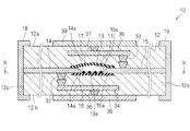
- Example 1-1 It is sectional drawing of an ESD protection device.
- Example 1-1 It is sectional drawing of an ESD protection device.
- Example 1-2 It is principal part sectional drawing of an ESD protection device.
- Example 2-1 It is principal part sectional drawing of an ESD protection device.
- Example 2-2 It is principal part sectional drawing of an ESD protection device.
- Example 3-1 It is principal part sectional drawing of an ESD protection device.
- Example 3-2 It is principal part sectional drawing of an ESD protection device.
- Example 4 It is principal part sectional drawing of an ESD protection device.
- Example 5-1 It is principal part sectional drawing of an ESD protection device.
- Example 5-2 It is principal part sectional drawing of an ESD protection device.
- Example It is principal part sectional drawing of an ESD protection device. (Conventional example)
- Example 1-1 An ESD protection device 10 of Example 1-1 will be described with reference to FIGS. 1 and 2.
- FIG. 1 An ESD protection device 10 of Example 1-1 will be described with reference to FIGS. 1 and 2.
- FIG. 1 is a cross-sectional view of the ESD protection device 10.
- FIG. 2 is a cross-sectional view of a principal part taken along line XX in FIG.
- the ESD protection device 10 includes a cavity portion 13 and a pair of discharge electrodes 14 formed inside a ceramic multilayer substrate 12 in which a plurality of ceramic layers are stacked in the vertical direction in FIG. 15.
- the discharge electrodes 14, 15 have opposing portions 14 a, 15 a that are formed along the inner surface of the cavity portion 13, are opposed to each other with an interval, and are exposed in the cavity portion 13.
- External electrodes 18 and 19 are formed on the end faces 12 p and 12 q of the ceramic multilayer substrate 12, and the external electrodes 18 and 19 are connected to the discharge electrodes 14 and 15.
- the external electrodes 18 and 19 are used for mounting the ESD protection device 10 on a circuit board or the like.
- conductor portions 34 and 35 disposed between the ceramic layers of the ceramic multilayer substrate 12 and via conductors 32 and 33; 36 and 37 penetrating the ceramic layers of the ceramic multilayer substrate 12 are provided. Is formed.
- the conductor portions 34 and 35 are connected to the discharge electrodes 14 and 15 via the via conductors 32 and 33.
- the conductor portions 34, 35, the via conductors 32, 33 and the discharge electrodes 14, 15 are conductors that conduct electricity and heat well, and the conductor portions 34, 35 are electrically connected to the discharge electrodes 14, 15.
- External conductor portions 38 and 39 are formed on the upper surface 12 a and the lower surface 12 b of the ceramic multilayer substrate 12.
- the external conductor portions 38 and 39 are connected to the conductor portions 34 and 35 via the via conductors 36 and 37.
- the conductor portions 34, 35, the via conductors 36, 37 and the external conductors 38, 39 are conductors that pass electricity and heat well, and the conductor portions 34, 35 are electrically connected to the external conductors 38, 39.
- Seal layers 16 and 17 are formed between the ceramic multilayer substrate 12 and the cavity 13.
- the sealing layers 16 and 17 are made of ceramics having a higher sintering temperature than the ceramics constituting the ceramic multilayer substrate 12, for example.
- the discharge assisting part 11 includes a dispersed metal material and a semiconductor material.
- assistant part 11 also in the area
- it may be formed on the opposing portions 14a, 15a of the discharge electrodes 14, 15 or between the opposing portions 14a, 15a of the discharge electrodes 14, 15 and the seal layer 16.
- the ESD protection device 10 when a voltage of a predetermined level or more is applied between the external electrodes 18 and 19, the discharge is generated in the cavity 13, that is, between the opposed portions 14 a and 15 a of the discharge electrodes 14 and 15. appear.
- Heat generated at the time of discharge is radiated from the conductor portions 34 and 35 to the outside of the ESD protection device 10 via the via conductors 36 and 37 and the external conductor portions 38 and 39, or from the conductor portions 34 and 35 to the via conductors 32, 33, The heat is radiated to the outside of the ESD protection device 10 through the discharge electrodes 14 and 15 and the external electrodes 18 and 19. By such heat radiation, it is possible to suppress the temperature rise of the facing portions 14a and 15a of the discharge electrodes 14 and 15.
- the opposing portions 14a and 15a of the discharge electrodes 14 and 15 are melted or peeled off due to repeated discharge, whereby the gap between the opposing portions 14a and 15a of the discharge electrodes 14 and 15 is increased, or the ball is turned into a ball and discharged. It can be suppressed that the gap between the opposed portions 14a and 15a of the electrodes 14 and 15 is substantially increased and the discharge characteristics are deteriorated.
- the glass component on the side opposite to the facing portions 14a and 15a of the discharge electrodes 14 and 15 with respect to the conductor portions 34 and 35 is transferred to the discharge electrodes 14 and 15 by the conductor portions 34 and 35. Movement toward the facing portions 14a and 15a and the discharge assisting portion 11 is prevented. This suppresses oversintering of the opposing portions 14a and 15a of the discharge electrodes 14 and 15 and the discharge assisting portion 11 due to the glass component, so It is possible to suppress discharge characteristic deterioration caused by sintering.
- the conductor portions 34 and 35 are disposed at a plurality of positions, that is, on both sides in the stacking direction of the ceramic layers of the ceramic multilayer substrate 12 with respect to the facing portions 14a and 15a of the discharge electrodes 14 and 15, heat dissipation and glass component diffusion suppression are performed. And can be performed more reliably.
- the conductor portions 34 and 35 broadly cover the opposing portions 14a and 15a of the discharge electrodes 14 and 15 along the opposite ends 14s and 15s of the opposing portions 14a and 15a of the discharge electrodes 14 and 15, and are seen through in the stacking direction. It is sometimes formed so as to cover the facing region 13s.
- the conductor portions 34 and 35 have a large area facing the tips 14s and 15s of the facing portions 14a and 15a of the discharge electrodes 14 and 15 that are opposite to each other, and have a high effect of releasing heat during discharge. It can be surely suppressed.
- Example 1-2 An ESD protection device 10a according to Example 1-2 will be described with reference to FIG.
- the ESD protection device 10a of Example 1-2 is configured in substantially the same manner as the ESD protection device 10 of Example 1-1.
- the same reference numerals are used for the same components as in the embodiment 1-1, and the description will focus on the differences from the embodiment 1-1.
- FIG. 3 is a cross-sectional view of the main part of the ESD protection device 10a.
- the ESD protection device 10a includes conductor portions 34a and 35a, external conductor portions 38a and 39a, and via conductors 32a arranged between the ceramic layers of the ceramic multilayer substrate 12 in the same manner as in Example 1-1.
- 33a; 36a, 37a, both of which are arranged on one side of the cavity 13, that is, on the opposite side of the cavity 13 in the stacking direction with respect to the opposing parts 14a, 15a of the discharge electrodes 14, 15. Yes.
- the conductor portions 34a and 35a are connected to the discharge electrodes 14 and 15 via the via conductors 32a and 33a, and are connected to the external conductor portions 38a and 39a via the via conductors 36a and 37a. Since the outer conductor portions 38a and 39a are sufficiently separated from each other, no discharge occurs between the outer conductor portions 38a and 39a.
- the conductor portions 34a and 35a are connected to the facing portions 14a of the discharge electrodes 14 and 15. , 15a to dissipate heat more effectively. Moreover, diffusion of the glass component can be more effectively suppressed. Since the conductor portions 34a and 35a are provided at a plurality of locations, it is possible to more reliably perform heat dissipation and suppression of glass component diffusion. Therefore, it is possible to suppress deterioration of discharge characteristics due to repeated discharge.
- Example 2-1 An ESD protection device 10b according to Example 2-1 will be described with reference to FIG.
- FIG. 4 is a cross-sectional view of the main part of the ESD protection device 10b.
- the conductor portions 34 and 35 disposed between the ceramic layers of the ceramic multilayer substrate 12 are arranged on the opposing portions 14a and 14a of the discharge electrodes 14 and 15, respectively. It is arranged on both sides in the stacking direction with respect to 15 a and is connected to the discharge electrodes 14 and 15 via via conductors 32 and 33.
- the external conductor portions 38 and 39 and the via conductors 36 and 37 that were in Example 1-1 (see FIG. 1) are not provided.
- the conductor portions 34 and 35 are disposed on both main surface sides of the facing portions 14a and 15a of the discharge electrodes 14 and 15, and the conductor portions 34 and 35 are connected to the discharge electrodes 14 and 15, Heat dissipation and suppression of diffusion of glass components can be performed more reliably. Therefore, it is possible to suppress deterioration of discharge characteristics due to repeated discharge.
- Example 2-2 An ESD protection device 10c of Example 2-2 will be described with reference to FIG.
- FIG. 5 is a cross-sectional view of the main part of the ESD protection device 10c.
- the ESD protection device 10c is similar to the embodiment 1-2 in that the cavity 13 is in one side of the cavity 13, that is, the opposing parts 14a and 15a of the discharge electrodes 14 and 15 in the stacking direction.
- Conductor portions 34a and 35a and via conductors 32a and 33a arranged on the opposite side are provided.
- the external conductor portions 38a and 39a and the via conductors 36a and 37a connected to the external conductor portions 38a and 39a, which were in the embodiment 1-2 (see FIG. 3), are not provided.
- the conductor portions 34a and 35a are connected to the facing portions 14a of the discharge electrodes 14 and 15. , 15a to dissipate heat more effectively. Moreover, diffusion of the glass component can be more effectively suppressed.
- the conductor portions 34a and 35a are provided at a plurality of locations, it is possible to more reliably suppress heat dissipation and diffusion of glass components. Therefore, it is possible to suppress deterioration of discharge characteristics due to repeated discharge.
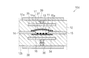
- Example 3-1 An ESD protection device 10d of Example 3-1 will be described with reference to FIG.
- FIG. 6 is a cross-sectional view of the main part of the ESD protection device 10d.
- the conductor portions 34 and 35 are connected to the external conductor portions 38 and 39 via the via conductors 36 and 37, as in the case of Example 1-1.
- the conductor portions 34 and 35 and the via conductors 32 and 33 connected to the discharge electrodes 14 and 15 in the embodiment 1-1 are not provided.
- the ESD protection device 10d is not electrically connected to the discharge electrodes 14 and 15 and the conductor portions 34 and 35, the via conductors 36 and 37, and the external conductor portions 38 and 39, the ESD protection device 10d can dissipate heat. The diffusion of components can be suppressed. Therefore, it is possible to suppress deterioration of discharge characteristics due to repeated discharge.
- Example 3-2 An ESD protection device 10e of Example 3-2 will be described with reference to FIG.
- FIG. 7 is a cross-sectional view of an essential part of the ESD protection device 10e cut along a position corresponding to the line XX in FIG.
- conductor portions 34e and 35e are arranged between ceramic layers of the ceramic multilayer substrate 12 on which the discharge electrodes 14 and 15 are arranged.
- the conductor portions 34e and 35e extend to the side surfaces 12s and 12t of the ceramic multilayer substrate 12, and are connected to the external conductor portions 38e and 39e formed on the side surfaces 12s and 12t of the ceramic multilayer substrate 12.
- the conductor portions 34e and 35e are formed in the stacking direction in which the ceramic layers of the ceramic multilayer substrate 12 are stacked (in the direction perpendicular to the paper surface in FIG. 7) and in the facing direction in which the facing portions 14a and 15a of the discharge electrodes 14 and 15 face each other (see FIG. 7).
- the opposing ends 14 a, 15 a of the discharge electrodes 14, 15 are covered with the opposite ends 14 s, 15 s and further discharged.
- the tip portions 14a and 15s of the facing portions 14a and 15a of the electrodes 14 and 15 are formed so as to cover the facing region 13s facing each other at the shortest distance.
- part of the heat generated during discharge is radiated from the conductor portions 34e and 35e to the outside of the ESD protection device 10e via the external conductor portions 38e and 39e.
- the temperature rise of 14a and 15a can be suppressed.
- the glass component diffusion at the time of baking can be suppressed by the conductor parts 34e and 35e. Therefore, it is possible to suppress deterioration of discharge characteristics due to repeated discharge.
- Example 4 An ESD protection device 10f of Example 4 will be described with reference to FIG.
- FIG. 8 is a cross-sectional view of the main part of the ESD protection device 10f.
- the ESD protection device 10f is disposed on both sides in the stacking direction of the cavity portion 13, that is, on both sides in the stacking direction with respect to the opposing portions 14a and 15a of the discharge electrodes 14 and 15, as in Example 1-1.
- the conductor parts 34 and 35 are provided.
- the external conductor portions 38 and 39 and the via conductors 32 and 33; 36 and 37 that are in the embodiment 1-1 (see FIG. 1) are not provided.
- the ESD protection device 10f a part of heat generated at the time of discharge is radiated from the opposing portions 14a, 15a of the discharge electrodes 14, 15 to the conductor portions 34, 35. Moreover, the conductor parts 34 and 35 can suppress glass component diffusion during firing. Therefore, it is possible to suppress deterioration of discharge characteristics due to repeated discharge.
- Example 5-1 An ESD protection device 10g of Example 5-1 will be described with reference to FIG.
- FIG. 9 is a sectional view of an essential part of the ESD protection device 10g.
- the ESD protection device 10g is similar to the fourth embodiment in that the cavity 13 is one side in the stacking direction of the cavity 13, that is, the cavity 13 in the stacking direction with respect to the opposing portions 14a and 15a of the discharge electrodes 14 and 15.
- a conductor portion 34 disposed on the opposite side is provided.
- the conductor part 35 which was in Example 4 (see FIG. 8) is not provided.
- the conductor portions 34 and 35 are connected to the facing portions 14a and 15a of the discharge electrodes 14 and 15, respectively. It is possible to dissipate heat more effectively by disposing the conductor portion 34 at a position closer to. Moreover, the conductor part 34 can suppress the glass component diffusion at the time of baking. Therefore, it is possible to suppress deterioration of discharge characteristics due to repeated discharge.
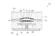
- Example 5-2 An ESD protection device 10h according to Example 5-2 will be described with reference to FIG.
- FIG. 10 is a cross-sectional view of the main part of the ESD protection device 10h.
- the ESD protection device 10 h includes the hollow portion 13 among the conductor portions 33, 34, the via conductors 36, 37, and the external conductor portions 38, 38 in the embodiment 3-1 (see FIG. 6).
- the conductor part 35, the via conductor 37, and the outer conductor part 39 arranged on the cavity part 13 side are not provided.
- the ESD protection device 10h can radiate heat from the conductor part 34 to the outside of the ESD protection device 10h via the external conductor part 38. Moreover, the conductor part 34 can suppress the glass component diffusion at the time of baking. Therefore, it is possible to suppress deterioration of discharge characteristics due to repeated discharge.
- the ceramic material used as the material of the ceramic layer of the ceramic multilayer substrate is a material having a composition centered on Ba, Al, and Si. Each material is prepared and mixed to have a predetermined composition, and calcined at 800-1000 ° C. The obtained calcined powder is pulverized with a zirconia ball mill for 12 hours to obtain a ceramic powder. To this ceramic powder, an organic solvent such as toluene and echinene is added and mixed. Further, a binder and a plasticizer are added and mixed to obtain a slurry. The slurry thus obtained is molded by a doctor blade method to obtain a ceramic green sheet having a thickness of 50 ⁇ m.
- the ceramic multilayer substrate In order for the ceramic multilayer substrate to contain a glass component, glass is added to the ceramic raw material powder in advance. You may use the ceramic raw material powder with which glass is produced
- an electrode paste for forming the discharge electrode is prepared.
- An electrode paste is obtained by adding a solvent to a binder resin composed of 80 wt% Cu powder having an average particle size of about 1.5 ⁇ m and ethyl cellulose, and stirring and mixing with a roll.
- the mixed paste for forming the discharge auxiliary part is prepared by mixing Cu powder having an average particle diameter of about 3 ⁇ m as a metal material and silicon carbide (SiC) having an average particle diameter of 1 ⁇ m as a semiconductor material at a predetermined ratio, and a binder resin and a solvent. It is obtained by adding and stirring with a roll and mixing.
- the binder resin and the solvent are 40 wt%, and the remaining 60 wt% is Cu powder and silicon carbide.
- the resin paste consists of a resin and a solvent.
- a resin that decomposes and disappears upon firing is used.
- PET polypropylene
- ethyl cellulose acrylic resin and the like.
- a seal layer forming paste for forming the seal layer is prepared by the same method as the electrode paste.
- a seal layer forming paste (alumina paste) is obtained by stirring and mixing a binder resin composed of 50 wt% Al 2 O 3 powder having an average particle diameter of about 1 ⁇ m, ethyl cellulose, and the like with a solvent and 50 w%.
- the solid component of the seal layer forming paste is not particularly limited as long as it has a higher sintering temperature than the ceramic material of the ceramic multilayer substrate.
- alumina, zirconia, magnesia, mullite, quartz or the like can be selected.
- the electrode paste is filled into the through hole by screen printing to form a portion that becomes a via conductor.
- the through hole may be formed using a mold.
- a seal layer forming paste is applied by screen printing on a ceramic green sheet that becomes a ceramic layer adjacent to the discharge electrode, thereby forming a portion that becomes a seal layer.
- the mixed paste is applied by screen printing so as to form a predetermined pattern on the ceramic green sheet that becomes one of the ceramic layers adjacent to the discharge electrode in order to form a discharge assisting portion.
- a concave portion provided in advance in the ceramic green sheet may be filled with the mixed paste of silicon carbide / Cu powder.
- electrode paste is applied by screen printing to form a discharge electrode having a facing portion.
- the discharge electrode was formed to have a thickness of 100 ⁇ m and a discharge gap width (a dimension of a distance between the opposed tips of the facing portions) of 30 ⁇ m.
- a resin paste is applied by screen printing in order to form a cavity on the top.
- an electrode paste is applied by screen printing on a ceramic green sheet that becomes one of the ceramic layers adjacent to the conductor part and the external conductor part, thereby forming the conductor part and the external conductor part. You may form a conductor part and an external conductor part using metal foil.
- the manufacturing process can be simplified, but other metals such as Al, Au, and Ni may be used. Use of Ag with high thermal conductivity is effective for heat dissipation.
- the conductor part and the outer conductor part are preferably thick and highly dense in order to improve heat dissipation and suppress glass diffusion.
- the denseness can be increased, and the thickness can be increased by increasing the solid content ratio of the conductive paste or by increasing the plate thickness of the printing pattern.
- the conductor part and the outer conductor part are formed of a metal foil, it is only necessary to increase the thickness of the metal foil.
- Firing Next firing is performed in an N 2 atmosphere in the same manner as a normal ceramic multilayer substrate.
- a rare gas such as Ar or Ne
- the temperature region in which the ceramic material is contracted and sintered may be fired in a rare gas atmosphere such as Ar and Ne.
- a rare gas atmosphere such as Ar and Ne.
- an electrode material such as Ag
- an air atmosphere may be used.
- the resin paste disappears and a cavity is formed. Moreover, the organic solvent in a ceramic green sheet, the binder resin in a mixed paste, and a solvent are also lose
- electrolytic Ni—Sn plating is performed on the external electrodes.
- the semiconductor material in the mixed paste is not particularly limited to the above materials.
- metal semiconductors such as silicon and germanium, carbides such as silicon carbide, titanium carbide, zirconium carbide, molybdenum carbide and tungsten carbide, nitrides such as titanium nitride, zirconium nitride, chromium nitride, vanadium nitride and tantalum nitride, titanium silicide , Silicides such as zirconium silicide, tungsten silicide, molybdenum silicide, chromium silicide, chromium silicide, titanium boride, zirconium boride, chromium boride, lanthanum boride, molybdenum boride, tungsten boride, etc.
- Oxides such as borides, zinc oxide, and strontium titanate can be used.
- silicon and silicon carbide are particularly preferable because they are relatively inexpensive and various particle size variations are commercially available.
- These semiconductor materials may be used alone or in admixture of two or more. Further, the semiconductor material may be used by appropriately mixing with a resistance material such as alumina or BAS material.
- the metal material in the mixed paste is not particularly limited to the above materials. Cu, Ag, Pd, Pt, Al, Ni, W, Mo, alloys thereof, or combinations thereof may be used.
- a resin paste is applied to form the hollow portion, but it is sufficient that the resin paste disappears even if it is not a resin, such as carbon. You may arrange
- the method of cutting before firing and dividing into chips was shown.
- the ceramic green sheets formed in an aggregated state are laminated and divided grooves are formed in the laminate formed by pressure bonding. After forming, firing, and plating, each chip may be cut.
- the ESD discharge response was evaluated for each sample.
- the ESD discharge responsiveness was measured by an electrostatic discharge immunity test defined in the IEC standard, IEC61000-4-2. 8 kV was applied by contact discharge, and the peak voltage during discharge was detected on the protection circuit side.
- ESD repeatability was evaluated.
- Application of 8 kV was performed 100 times by contact discharge, and then the discharge responsiveness to the ESD was evaluated.
- ESD voltage resistance is poor when the peak voltage detected on the protection circuit side is 700V or more (x mark), peak voltage is 600V or more and less than 700V is good (circle mark), and peak voltage is particularly good when the peak voltage is less than 600V ( ⁇ ).
- Table 1 below shows the evaluation results.
- the unit of the numerical value (peak voltage) in the “ESD discharge responsiveness” column and the “ESD repetition resistance” column is V.
- each example shows improvement in the initial ESD discharge response.
- a heat radiating conductor electrode
- the former having higher heat dissipation improves the ESD repeatability than the latter.
- Example 1-1 FIG. 1
- Example 3-1 FIG. 6
- Example 2-1 FIG. 4
- the heat-dissipating conductor is connected to the discharge electrode
- the heat-dissipating conductor is connected to the external conductor
- the heat-dissipating conductor is connected to the opposite side of the discharge electrode from both sides.
- the heat dissipating effect is enhanced by arranging the heat-dissipating conductor part so that it is covered not in the same layer as the opposite part of the discharge electrode but in the stacking direction. , ESD repeatability is improved.
- the body of the ESD protection device is not limited to a ceramic multilayer substrate, and may be an insulating multilayer substrate in which an insulating layer such as a resin is laminated.
- the conductor portion may be configured such that the width of the portion covering the facing portion of one discharge electrode is different from the width of the portion covering the facing portion of the other discharge electrode. For example, since heat is generated at the facing portion of the discharge electrode on the side receiving electrons during discharge, the width of the portion covering the facing portion of the discharge electrode on the side receiving electrons during discharging covers the facing portion of the other discharge electrode If the conductor portion is formed so as to be larger than the width of the substrate and heat dissipation is promoted, deterioration of the discharge characteristics can be suppressed more reliably.
- the conductor portions are collectively placed on the side where the number of ceramic layers of the ceramic multilayer substrate is relatively large with respect to the discharging electrode. Then, it is more effective.
- the cavity is preferably disposed on the side opposite to the conductor, that is, on the side where the number of ceramic layers of the ceramic multilayer substrate is relatively small with respect to the portion facing the discharge electrode.
- Discharge auxiliary part 12 Ceramic multilayer substrate 12a Upper surface 12b Lower surface 12p, 12q End surface (surface) 12s, 12t Side surface 13 Cavity portion 13s Opposing region 14 Discharge electrode 14a Opposing portion 14s Tip 15 Discharge electrode 15a Opposing portion 15s Tip 15 Conductor portion 16, 17 Seal layer 18, 19 External electrode 32, 32a Via conductor 33, 33a Via conductor 33 , 34 Conductor part 34 Conductor part 34, 35 Conductor part 34a, 35a Conductor part 34e, 35e Conductor part 35 Conductor part 36 Via conductor 36, 36a Via conductor 37, 37a Via conductor 38, 38a, 38e External conductor part 39, 39a, 39e outer conductor
Landscapes
- Structure Of Printed Boards (AREA)
- Production Of Multi-Layered Print Wiring Board (AREA)
- Ceramic Capacitors (AREA)
Abstract
La présente invention se rapporte à un dispositif de protection contre les décharges électrostatiques avec lequel il est possible de réduire la dégradation des caractéristiques de décharge résultant de décharges répétées et l'excès de frittage résultant de la diffusion d'un composant de verre. Une partie creuse (13), au moins une paire d'électrodes de décharge (14, 15) et des parties conductrices (34, 35) sont formées à l'intérieur d'un substrat isolant à plusieurs couches (12) dans lequel sont empilées une pluralité de couches isolantes. Les électrodes de décharge (14, 15) sont pourvues de parties en vis-à-vis (14a, 15a) qui sont formées le long des faces intérieures de la partie creuse (13), un espace étant agencé entre ces dernières, et qui se font face. Les électrodes de décharge (14, 15) sont, de plus, raccordées à des électrodes extérieures (18, 19). Les parties conductrices (34, 35) sont formées de sorte à couvrir au moins l'une des extrémités avant opposées (14s, 15s) des parties en vis-à-vis (14a, 15a) des électrodes de décharge (14, 15) lorsqu'on regarde dans la direction d'empilement dans laquelle sont empilées les couches isolantes du substrat isolant à plusieurs couches (12), dans la direction de vis-à-vis dans laquelle les parties en vis-à-vis (14a, 15a) des électrodes de décharge (14, 15) se font face, ou dans une direction qui est perpendiculaire à la fois à la direction d'empilement et à la direction de vis-à-vis.
Priority Applications (2)
| Application Number | Priority Date | Filing Date | Title |
|---|---|---|---|
| JP2013541778A JP5741708B2 (ja) | 2011-11-01 | 2012-10-30 | Esd保護デバイス |
| US14/267,483 US9590417B2 (en) | 2011-11-01 | 2014-05-01 | ESD protective device |
Applications Claiming Priority (2)
| Application Number | Priority Date | Filing Date | Title |
|---|---|---|---|
| JP2011-239961 | 2011-11-01 | ||
| JP2011239961 | 2011-11-01 |
Related Child Applications (1)
| Application Number | Title | Priority Date | Filing Date |
|---|---|---|---|
| US14/267,483 Continuation US9590417B2 (en) | 2011-11-01 | 2014-05-01 | ESD protective device |
Publications (1)
| Publication Number | Publication Date |
|---|---|
| WO2013065672A1 true WO2013065672A1 (fr) | 2013-05-10 |
Family
ID=48192019
Family Applications (1)
| Application Number | Title | Priority Date | Filing Date |
|---|---|---|---|
| PCT/JP2012/078009 Ceased WO2013065672A1 (fr) | 2011-11-01 | 2012-10-30 | Dispositif de protection contre les décharges électrostatiques |
Country Status (3)
| Country | Link |
|---|---|
| US (1) | US9590417B2 (fr) |
| JP (1) | JP5741708B2 (fr) |
| WO (1) | WO2013065672A1 (fr) |
Cited By (5)
| Publication number | Priority date | Publication date | Assignee | Title |
|---|---|---|---|---|
| WO2016129317A1 (fr) * | 2015-02-10 | 2016-08-18 | 株式会社村田製作所 | Structure de protection contre les décharges électrostatiques et son procédé de production |
| WO2016208383A1 (fr) * | 2015-06-22 | 2016-12-29 | 株式会社村田製作所 | Dispositif de protection contre les décharges électrostatiques et procédé de fabrication de dispositif de protection contre les décharges électrostatiques |
| JP2017010850A (ja) * | 2015-06-24 | 2017-01-12 | 株式会社村田製作所 | Esd保護装置 |
| JP2023003099A (ja) * | 2021-06-23 | 2023-01-11 | Tdk株式会社 | 過渡電圧保護デバイス |
| JP2023005443A (ja) * | 2021-06-29 | 2023-01-18 | Tdk株式会社 | 過渡電圧保護デバイス |
Families Citing this family (8)
| Publication number | Priority date | Publication date | Assignee | Title |
|---|---|---|---|---|
| JP5991453B1 (ja) * | 2014-11-19 | 2016-09-14 | 株式会社村田製作所 | Esd保護素子、およびesd保護素子付きコモンモードチョークコイル |
| DE102015116278A1 (de) * | 2015-09-25 | 2017-03-30 | Epcos Ag | Überspannungsschutzbauelement und Verfahren zur Herstellung eines Überspannungsschutzbauelements |
| CN109891680B (zh) * | 2016-11-04 | 2021-11-16 | 阿莫技术有限公司 | 功能性接触器 |
| CN109891679B (zh) | 2016-11-04 | 2021-11-02 | 阿莫技术有限公司 | 功能性接触器 |
| KR102565034B1 (ko) | 2016-11-09 | 2023-08-09 | 주식회사 아모텍 | 기능성 컨택터 |
| WO2024206934A1 (fr) * | 2023-03-31 | 2024-10-03 | Ppc Broadband, Inc. | Éclateur de circuit imprimé à tension d'amorçage améliorée pour protéger un dispositif électronique connecté à l'éclateur |
| FR3161815A1 (fr) | 2024-04-30 | 2025-10-31 | Safran Electronics & Defense | Dispositif de protection pour composant électronique, système de protection et circuit électronique associés |
| FR3161816A1 (fr) | 2024-04-30 | 2025-10-31 | Safran Electronics & Defense | Dispositif de protection pour composant électronique, système de protection et circuit électronique associés |
Citations (4)
| Publication number | Priority date | Publication date | Assignee | Title |
|---|---|---|---|---|
| JP2003123936A (ja) * | 2001-10-16 | 2003-04-25 | Matsushita Electric Ind Co Ltd | 電子部品およびその製造方法 |
| JP2009016616A (ja) * | 2007-07-05 | 2009-01-22 | Tdk Corp | サージ吸収素子及び発光装置 |
| WO2009136535A1 (fr) * | 2008-05-08 | 2009-11-12 | 株式会社 村田製作所 | Substrat incorporant une fonction de protection contre les décharges électrostatiques |
| WO2011040435A1 (fr) * | 2009-09-30 | 2011-04-07 | 株式会社村田製作所 | Dispositif de protection contre les décharges électrostatiques et procédé de fabrication associé |
Family Cites Families (3)
| Publication number | Priority date | Publication date | Assignee | Title |
|---|---|---|---|---|
| JP2008146514A (ja) | 2006-12-13 | 2008-06-26 | Canon Inc | 情報処理装置、情報処理装置の制御方法、および情報処理装置の制御プログラム |
| CN101933204B (zh) * | 2008-02-05 | 2015-06-03 | 株式会社村田制作所 | Esd保护器件 |
| EP2352211B1 (fr) * | 2008-11-26 | 2017-12-20 | Murata Manufacturing Co. Ltd. | Dispositif de protection contre les decharges electrostatiques et son procede de fabrication |
-
2012
- 2012-10-30 WO PCT/JP2012/078009 patent/WO2013065672A1/fr not_active Ceased
- 2012-10-30 JP JP2013541778A patent/JP5741708B2/ja active Active
-
2014
- 2014-05-01 US US14/267,483 patent/US9590417B2/en active Active
Patent Citations (4)
| Publication number | Priority date | Publication date | Assignee | Title |
|---|---|---|---|---|
| JP2003123936A (ja) * | 2001-10-16 | 2003-04-25 | Matsushita Electric Ind Co Ltd | 電子部品およびその製造方法 |
| JP2009016616A (ja) * | 2007-07-05 | 2009-01-22 | Tdk Corp | サージ吸収素子及び発光装置 |
| WO2009136535A1 (fr) * | 2008-05-08 | 2009-11-12 | 株式会社 村田製作所 | Substrat incorporant une fonction de protection contre les décharges électrostatiques |
| WO2011040435A1 (fr) * | 2009-09-30 | 2011-04-07 | 株式会社村田製作所 | Dispositif de protection contre les décharges électrostatiques et procédé de fabrication associé |
Cited By (12)
| Publication number | Priority date | Publication date | Assignee | Title |
|---|---|---|---|---|
| WO2016129317A1 (fr) * | 2015-02-10 | 2016-08-18 | 株式会社村田製作所 | Structure de protection contre les décharges électrostatiques et son procédé de production |
| CN107112726A (zh) * | 2015-02-10 | 2017-08-29 | 株式会社村田制作所 | 静电放电保护构造体以及其制造方法 |
| JPWO2016129317A1 (ja) * | 2015-02-10 | 2017-08-31 | 株式会社村田製作所 | 静電気放電保護構造体およびその製造方法 |
| CN107112726B (zh) * | 2015-02-10 | 2019-01-29 | 株式会社村田制作所 | 静电放电保护构造体以及其制造方法 |
| WO2016208383A1 (fr) * | 2015-06-22 | 2016-12-29 | 株式会社村田製作所 | Dispositif de protection contre les décharges électrostatiques et procédé de fabrication de dispositif de protection contre les décharges électrostatiques |
| JPWO2016208383A1 (ja) * | 2015-06-22 | 2017-12-28 | 株式会社村田製作所 | Esd保護装置およびesd保護装置の製造方法 |
| US10320154B2 (en) | 2015-06-22 | 2019-06-11 | Murata Manufacturing Co., Ltd. | ESD protection device and manufacturing method for ESD protection device |
| JP2017010850A (ja) * | 2015-06-24 | 2017-01-12 | 株式会社村田製作所 | Esd保護装置 |
| JP2023003099A (ja) * | 2021-06-23 | 2023-01-11 | Tdk株式会社 | 過渡電圧保護デバイス |
| JP7322925B2 (ja) | 2021-06-23 | 2023-08-08 | Tdk株式会社 | 過渡電圧保護デバイス |
| JP2023005443A (ja) * | 2021-06-29 | 2023-01-18 | Tdk株式会社 | 過渡電圧保護デバイス |
| JP7425976B2 (ja) | 2021-06-29 | 2024-02-01 | Tdk株式会社 | 過渡電圧保護デバイス |
Also Published As
| Publication number | Publication date |
|---|---|
| US9590417B2 (en) | 2017-03-07 |
| JP5741708B2 (ja) | 2015-07-01 |
| JPWO2013065672A1 (ja) | 2015-04-02 |
| US20140240878A1 (en) | 2014-08-28 |
Similar Documents
| Publication | Publication Date | Title |
|---|---|---|
| JP5741708B2 (ja) | Esd保護デバイス | |
| JP4434314B2 (ja) | Esd保護デバイス | |
| US8711537B2 (en) | ESD protection device and method for producing the same | |
| JP5557060B2 (ja) | Esd保護装置の製造方法 | |
| JP5590122B2 (ja) | Esd保護デバイス | |
| JPWO2010067503A1 (ja) | Esd保護デバイス | |
| JP5403370B2 (ja) | Esd保護装置 | |
| JP5660412B2 (ja) | Esd保護デバイス | |
| JP5954447B2 (ja) | Esd保護装置 | |
| JP5614315B2 (ja) | Esd保護装置 | |
| JP5403075B2 (ja) | Esd保護装置 | |
| CN105164875B (zh) | Esd保护装置 | |
| JP5605413B2 (ja) | Esd保護デバイスとその製造方法 | |
| WO2013146324A1 (fr) | Dispositif de protection contre les décharges électrostatiques et procédé de production associé |
Legal Events
| Date | Code | Title | Description |
|---|---|---|---|
| 121 | Ep: the epo has been informed by wipo that ep was designated in this application |
Ref document number: 12845729 Country of ref document: EP Kind code of ref document: A1 |
|
| ENP | Entry into the national phase |
Ref document number: 2013541778 Country of ref document: JP Kind code of ref document: A |
|
| NENP | Non-entry into the national phase |
Ref country code: DE |
|
| 122 | Ep: pct application non-entry in european phase |
Ref document number: 12845729 Country of ref document: EP Kind code of ref document: A1 |