WO2013073242A1 - 周期的構造体、および、それを用いた測定方法 - Google Patents
周期的構造体、および、それを用いた測定方法 Download PDFInfo
- Publication number
- WO2013073242A1 WO2013073242A1 PCT/JP2012/070878 JP2012070878W WO2013073242A1 WO 2013073242 A1 WO2013073242 A1 WO 2013073242A1 JP 2012070878 W JP2012070878 W JP 2012070878W WO 2013073242 A1 WO2013073242 A1 WO 2013073242A1
- Authority
- WO
- WIPO (PCT)
- Prior art keywords
- periodic structure
- electromagnetic wave
- measured
- resonance
- gap
- Prior art date
- Legal status (The legal status is an assumption and is not a legal conclusion. Google has not performed a legal analysis and makes no representation as to the accuracy of the status listed.)
- Ceased
Links
Images









Classifications
-
- G—PHYSICS
- G01—MEASURING; TESTING
- G01N—INVESTIGATING OR ANALYSING MATERIALS BY DETERMINING THEIR CHEMICAL OR PHYSICAL PROPERTIES
- G01N21/00—Investigating or analysing materials by the use of optical means, i.e. using sub-millimetre waves, infrared, visible or ultraviolet light
- G01N21/01—Arrangements or apparatus for facilitating the optical investigation
-
- G—PHYSICS
- G01—MEASURING; TESTING
- G01N—INVESTIGATING OR ANALYSING MATERIALS BY DETERMINING THEIR CHEMICAL OR PHYSICAL PROPERTIES
- G01N21/00—Investigating or analysing materials by the use of optical means, i.e. using sub-millimetre waves, infrared, visible or ultraviolet light
- G01N21/17—Systems in which incident light is modified in accordance with the properties of the material investigated
- G01N21/25—Colour; Spectral properties, i.e. comparison of effect of material on the light at two or more different wavelengths or wavelength bands
- G01N21/31—Investigating relative effect of material at wavelengths characteristic of specific elements or molecules, e.g. atomic absorption spectrometry
- G01N21/35—Investigating relative effect of material at wavelengths characteristic of specific elements or molecules, e.g. atomic absorption spectrometry using infrared light
- G01N21/3581—Investigating relative effect of material at wavelengths characteristic of specific elements or molecules, e.g. atomic absorption spectrometry using infrared light using far infrared light; using Terahertz radiation
- G01N21/3586—Investigating relative effect of material at wavelengths characteristic of specific elements or molecules, e.g. atomic absorption spectrometry using infrared light using far infrared light; using Terahertz radiation by Terahertz time domain spectroscopy [THz-TDS]
-
- G—PHYSICS
- G01—MEASURING; TESTING
- G01N—INVESTIGATING OR ANALYSING MATERIALS BY DETERMINING THEIR CHEMICAL OR PHYSICAL PROPERTIES
- G01N21/00—Investigating or analysing materials by the use of optical means, i.e. using sub-millimetre waves, infrared, visible or ultraviolet light
- G01N21/75—Systems in which material is subjected to a chemical reaction, the progress or the result of the reaction being investigated
- G01N21/77—Systems in which material is subjected to a chemical reaction, the progress or the result of the reaction being investigated by observing the effect on a chemical indicator
- G01N21/7703—Systems in which material is subjected to a chemical reaction, the progress or the result of the reaction being investigated by observing the effect on a chemical indicator using reagent-clad optical fibres or optical waveguides
- G01N21/774—Systems in which material is subjected to a chemical reaction, the progress or the result of the reaction being investigated by observing the effect on a chemical indicator using reagent-clad optical fibres or optical waveguides the reagent being on a grating or periodic structure
Definitions
- the present invention relates to a periodic structure and a measurement method using the same.
- an object to be measured is held in a void arrangement structure (periodic structure), an electromagnetic wave is irradiated to the periodic structure on which the object to be measured is held, A method of measuring a characteristic of an object to be measured by analyzing a transmittance spectrum is used. Specifically, for example, there is a method of analyzing a transmittance spectrum by irradiating a terahertz wave to a metal mesh to which a protein to be measured is attached.
- Patent Document 1 International Publication No. 2011/027642
- the polarization direction of electromagnetic waves is applied to a flat periodic structure having a plurality of voids that are not mirrored with respect to a certain virtual surface.
- a method of irradiating an electromagnetic wave so as to be orthogonal to a virtual plane and measuring a characteristic of an object to be measured based on a change in frequency characteristic of the electromagnetic wave scattered by a periodic structure is disclosed.
- Non-Patent Document 1 (Dai Onishi et al., “Optical characteristics of gold nano slit ring structure having plasmon resonance frequency in terahertz band”, Nanotech Japan, Focus 26 ⁇ 11th> Optical characteristics of gold nano slit ring structure, 2010 On October 8, 1980, Vol.3, No.5), a structure in which nano slit rings having gaps (slits) are periodically arranged on a substrate has a plasmon resonance frequency in the terahertz band. It is disclosed.
- Non-Patent Document 1 since resonators such as independent slit rings are periodically arranged on the substrate, it is necessary to adjust and optimize the interval between the resonators in order to obtain desired characteristics. there were. Since this interval is very small (approximately 1/10) compared to the size of the resonator, the variation becomes large during actual manufacturing. For this reason, when the structure described in Non-Patent Document 1 is irradiated with an electromagnetic wave such as a terahertz wave, many unnecessary resonances occur, and it is difficult to detect the object to be measured based on the change in the scattering spectrum. It is done.
- an electromagnetic wave such as a terahertz wave
- An object of the present invention is to provide a periodic structure as a highly sensitive measuring device capable of measuring various kinds of objects to be measured in various amounts independently, and a measuring method using the periodic structure. .
- the present invention is a plate-like periodic structure in which at least two voids penetrating in a direction perpendicular to the main surface are periodically arranged in at least one direction on the main surface,
- the shape of the gap is a shape that is not mirror-symmetric with respect to a virtual surface that is one of the surfaces orthogonal to the main surface,
- the gap portion has a constricted portion in which a gap interval which is a width in a direction parallel to an intersection line of the main surface and the virtual surface is partially narrowed. is there.
- the periodic structure of the present invention holds an object to be measured in the periodic structure, Irradiating linearly polarized electromagnetic waves in a direction perpendicular to the main surface of the periodic structure, Detecting electromagnetic waves forward scattered or back scattered by the periodic structure,
- the dip waveform generated in the frequency characteristic of the forward-scattered electromagnetic wave or the peak waveform generated in the frequency characteristic of the back-scattered electromagnetic wave varies depending on the presence of the object to be measured. It is preferably used in a measurement method for measuring.
- the gap interval on both sides of the constricted portion is wider than that of the constricted portion.
- the present invention holds the object to be measured in the above periodic structure, Irradiating linearly polarized electromagnetic waves in a direction perpendicular to the main surface of the periodic structure, Detecting electromagnetic waves forward scattered or back scattered by the periodic structure, The dip waveform generated in the frequency characteristic of the forward-scattered electromagnetic wave or the peak waveform generated in the frequency characteristic of the back-scattered electromagnetic wave varies depending on the presence of the object to be measured. It also relates to a measuring method characterized by measuring.
- the resonance generated by the first step is a TE11 mode-like resonance and the resonance generated by the second step is an LC resonance.
- the frequency of the dip waveform or the peak waveform based on the resonance generated by the second step is 1/10 to 10 times the frequency of the dip waveform or the peak waveform based on the resonance generated by the first step. Furthermore, it is preferable that the width of the constricted portion in the direction parallel to the intersection line between the main surface and the virtual surface is adjusted.
- a dip waveform caused by resonance in two different modes for example, TE11 mode-like resonance and LC resonance
- a variety of objects to be measured can be measured. That is, it is possible to detect an object to be measured based on another measurement principle using one periodic structure.
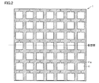
- FIG. 2 is a front view showing a periodic structure according to Embodiment 1.
- FIG. It is a front view which shows the unit structure of the periodic structure shown in FIG. 6 is a front view showing a periodic structure according to Embodiment 2.
- FIG. 10 is a front view showing a periodic structure according to Embodiment 3.
- FIG. It is a front view which shows another example of the periodic structure of Embodiment 3.
- 2 is a diagram showing a transmittance spectrum obtained in Example 1.
- FIG. (A), (b) is an electric field strength distribution diagram when irradiating the electromagnetic wave of the frequency in the dip waveform at the time of irradiating the Y polarized wave of FIG. (C), (d) is an electric field strength distribution diagram when the electromagnetic wave of the frequency in the dip waveform at the time of irradiating Z polarization is irradiated.
- 6 is a diagram showing a transmittance spectrum of Y-polarized light obtained in Example 2.
- FIG. 6 is a diagram showing a transmittance spectrum of Z-polarized light obtained in Example 2.
- FIG. (A) is a perspective view which shows the unit structure of the periodic structure shown in FIG.
- FIG. 6 is a front view showing a periodic structure of Comparative Example 1.
- FIG. 6 is a front view showing a unit structure of a periodic structure in Comparative Example 1.
- FIG. 6 is a diagram showing a transmittance spectrum obtained in Comparative Example 1.
- FIG. It is a figure which shows the transmittance
- FIG. It is a figure which shows the transmittance
- FIG. 1 is a schematic diagram showing the overall structure of a measuring apparatus used in the measuring method of the present invention.
- This measuring apparatus uses an electromagnetic wave (for example, a terahertz wave having a frequency of 20 GHz to 120 THz) generated by irradiating a semiconductor material with laser light emitted from a laser 7 (for example, a short light pulse laser). It is.
- an electromagnetic wave for example, a terahertz wave having a frequency of 20 GHz to 120 THz
- a laser 7 for example, a short light pulse laser
- the laser light emitted from the laser 7 is branched into two paths by the half mirror 70.
- One is irradiated to the photoconductive element 77 on the electromagnetic wave generation side, and the other is a plurality of mirrors 71 (numbering is omitted for the same function), so that the light on the reception side passes through the time delay stage 76.
- the conductive element 78 is irradiated.
- the photoconductive elements 77 and 78 a general element in which a dipole antenna having a gap portion is formed in LT-GaAs (low temperature growth GaAs) can be used.
- a fiber type laser a laser using a solid such as titanium sapphire, or the like can be used.
- the semiconductor surface may be used without an antenna, or an electro-optic crystal such as a ZnTe crystal may be used.
- an appropriate bias voltage is applied by the power supply 80 to the gap portion of the photoconductive element 77 on the generation side.
- the generated electromagnetic wave is made into a parallel beam by the parabolic mirror 72 and irradiated to the periodic structure 1 by the parabolic mirror 73.
- the periodic structure 1 may remain in a concave portion of a measuring device (microplate) described later, and is removed from the measuring device (microplate). Also good.
- the terahertz wave transmitted through the periodic structure 1 is received by the photoconductive element 78 by the parabolic mirrors 74 and 75.
- the electromagnetic wave signal received by the photoconductive element 78 is amplified by the amplifier 84 and then acquired through the lock-in amplifier 82.
- a signal processing such as Fourier transform is performed by a PC (personal computer) 83 including a calculating means
- the transmittance spectrum of the periodic structure 1 is calculated.
- the bias voltage from the power supply 80 applied to the gap of the photoconductive element 77 on the generation side is modulated (amplitude 5V to 30V) by the signal of the oscillator 81.
- the S / N ratio can be improved by performing synchronous detection.
- THz-TDS terahertz time domain spectroscopy
- FT-IR Fourier transform infrared spectroscopy
- FIG. 1 shows the case where the transmittance of electromagnetic waves is measured, but in the present invention, the reflectance of electromagnetic waves may be measured.
- the transmittance in transmission in the zeroth direction and the reflectance in reflection in the zeroth direction are measured.
- the grating interval of the diffraction grating is s
- the incident angle is i
- the diffraction angle is ⁇
- the wavelength is ⁇
- the electromagnetic wave used in the measurement method of the present invention is preferably an electromagnetic wave (terahertz wave) having a wavelength ⁇ of 0.3 ⁇ m to 15 mm (frequency: 20 GHz to 1 PHz).
- ahertz wave having a wavelength ⁇ of 0.3 ⁇ m to 15 mm (frequency: 20 GHz to 1 PHz).
- the electromagnetic wave examples include a terahertz wave generated by a light rectifying effect of an electro-optic crystal such as ZnTe using a short light pulse laser as a light source.
- an electro-optic crystal such as ZnTe
- a terahertz wave emitted from a high-pressure mercury lamp or a high-temperature ceramic can be used.
- Specific examples of the electromagnetic wave include visible light emitted from a semiconductor laser or a photodiode.
- the electromagnetic wave irradiated to the periodic structure in the measurement method of the present invention is preferably a linearly polarized electromagnetic wave.
- the linearly polarized electromagnetic wave may be a linearly polarized electromagnetic wave emitted from a non-polarized light or a circularly polarized light source after passing through a (linear) polarizer, or a linearly polarized electromagnetic wave emitted from a polarized light source. It may be.
- a wire grid etc. can be used as a linear polarizer.
- “measuring the characteristics of an object to be measured” means performing various qualities such as quantification and dielectric constant of a compound to be measured, for example, a small amount of an object to be measured such as in a solution.
- the case of measuring the content of or the case of identifying the object to be measured Specifically, for example, the periodic structure is immersed in a solution in which the object to be measured is dissolved, and after the object to be measured is attached to the surface of the periodic structure, the solvent and excess object to be measured are washed, The method of measuring the characteristic of a to-be-measured object using the above measuring apparatuses after drying a structural body is mentioned.
- the amount of the object to be measured is determined by comparing with a calibration curve created based on frequency characteristics obtained by measuring various amounts of the object to be measured in advance. It is preferable to calculate.
- the periodic structure of the present invention is a plate-like periodic structure in which at least two voids penetrating in a direction perpendicular to the main surface are periodically arranged in at least one direction on the main surface.
- all of the voids may be periodically arranged, and within a range that does not impair the effects of the present invention, some of the voids are periodically arranged and other voids are aperiodic. May be arranged.
- the periodic structure according to the present invention is characterized in that (1) the shape of the gap is not mirror-symmetrical with respect to a virtual plane that is one of the surfaces orthogonal to the main surface, and (2) The gap portion has a constricted portion.
- the “constricted portion” means a portion where the width (gap interval) in the direction parallel to the intersection line between the main surface of the periodic structure and the virtual surface is partially narrowed.
- the electric field direction of the electromagnetic wave coincides with the electric field direction at the time of resonance of the constricted portion.
- LC resonance occurs because energy transfer to the LC resonator occurs.
- the gap is wide on both sides of the constricted portion.
- the LC resonance becomes stronger and the sensitivity of the measurement using the LC resonance is improved compared to the case where the gap interval is wide only on one side of the constricted portion (when the constricted portion is at the end of the gap). To do.
- the periodic structure is preferably a quasi-periodic structure or a periodic structure.
- a quasi-periodic structure is a structure that does not have translational symmetry but is maintained in order. Examples of the quasi-periodic structure include a Fibonacci structure as a one-dimensional quasi-periodic structure and a Penrose structure as a two-dimensional quasi-periodic structure.
- a periodic structure is a structure having spatial symmetry as represented by translational symmetry. One-dimensional periodic structure, two-dimensional periodic structure, and three-dimensional periodic structure according to the symmetry dimension. Classified into the body. Examples of the one-dimensional periodic structure include a wire grid structure and a one-dimensional diffraction grating. Examples of the two-dimensional periodic structure include a mesh filter and a two-dimensional diffraction grating. Among these periodic structures, a two-dimensional periodic structure is preferably used.
- the characteristic of the object to be measured is measured based on at least one parameter related to the frequency characteristic of the electromagnetic wave scattered by the periodic structure.
- the dip waveform generated in the frequency characteristic of the electromagnetic wave forward scattered (transmitted) by the periodic structure, the peak waveform generated in the frequency characteristic of the electromagnetic wave dispersed backward (reflected), and the like change depending on the presence of the object to be measured.
- the characteristics of the object to be measured can be measured based on the above.
- the dip waveform is a frequency characteristic (for example, transmittance spectrum) of the periodic structure in a frequency range in which the ratio of the detected electromagnetic wave to the irradiated electromagnetic wave (for example, the transmittance of the electromagnetic wave) is relatively large. It is the waveform of the part of the valley type (convex downward) seen partially.
- the peak waveform is a part of the frequency characteristic (for example, reflectance spectrum) of the periodic structure in a frequency range in which the ratio of the detected electromagnetic wave to the irradiated electromagnetic wave (for example, the reflectance of the electromagnetic wave) is relatively small. It is a mountain-shaped (convex upward) waveform.
- the polarization direction is perpendicular to the virtual plane when each gap is regarded as a waveguide.
- LC resonance Is preferably generated.
- the TE11 mode-like resonance includes TE11 mode resonance and mode resonance similar to the TE11 mode.
- the dip waveform in the frequency characteristic of the forward scattered electromagnetic wave or the peak waveform in the frequency characteristic of the back scattered electromagnetic wave becomes sharp and the measurement sensitivity is improved. is there.
- the frequency shift amount of the dip waveform or peak waveform before and after the object to be measured is held on the periodic structure increases, the measurement sensitivity of the object to be measured can be improved.
- the measurement sensitivity is improved in the second step. That is, in the first step, a sample having an extremely small size is measured with respect to a portion having a TE11 mode electric field, that is, the space size of the entire void arrangement structure, whereas in the second step, Since a very small sample is measured using a space size (electric field generated there) that is narrower than the entire metal mesh around the constricted portion, the sensitivity is improved.
- the periodic structure of the present invention can detect a dip waveform generated by resonance in two different modes (for example, TE11 mode-like resonance and LC resonance) by changing the polarization direction.
- Various objects can be measured in various quantities with the periodic structure. That is, measurement can be performed with two sensitivities using one sensor.
- a measurement object is arranged at a position, and a first step of performing measurement by irradiating a first electromagnetic wave (Z polarized wave) whose polarization direction is perpendicular to the virtual plane is performed.
- Z polarized wave a first electromagnetic wave
- the size of the gap is appropriately designed according to the measurement method, the material properties of the periodic structure, the frequency of the electromagnetic wave used, etc., and it is difficult to generalize the range, but the electromagnetic wave scattered forward
- the lattice spacing of the gaps (for example, P shown in FIG. 3) is 1/10 or more of the wavelength of the electromagnetic wave used for measurement. It is preferably 10 times or less. When the lattice spacing of the gap is outside this range, scattering may be difficult to occur.
- gap part is 1/10 or more and 10 times or less of the wavelength of the electromagnetic waves used for a measurement. If the pore size of the gap is out of this range, the intensity of the transmitted (forward scattered) electromagnetic wave becomes weak and it may be difficult to detect the signal.
- the frequency of the dip waveform or peak waveform based on the resonance generated by the second step is 1/10 to 10 times the frequency of the dip waveform or peak waveform based on the resonance generated by the first step. It is preferable that the gap interval of the constricted part (notch part, slit) is adjusted. Thereby, it becomes possible to measure the first step and the second step simultaneously or individually using the same measuring device, and the device cost can be reduced.
- the average thickness of the periodic structure is appropriately designed according to the measurement method, the material characteristics of the periodic structure, the frequency of the electromagnetic wave used, etc., but it is difficult to generalize the range.
- it is preferably not more than several times the wavelength of the electromagnetic wave used for measurement. If the average thickness of the structure is larger than this range, the intensity of the electromagnetic waves scattered forward becomes weak and it may be difficult to detect the signal.
- the periodic structure of the present invention usually has a structure in which the entire structure is integrally coupled. Therefore, individual resonators such as fine rings like the structure described in Non-Patent Document 1 are used. It is not necessary to adjust the interval between the resonators, which is necessary when the resonators are periodically arranged, and the influence of unnecessary resonance caused by the interval between the resonators is small (or absent).
- the object may be directly attached to the periodic structure via a support film or the like. It may be attached. From the viewpoint of performing measurement with high reproducibility by improving measurement sensitivity and suppressing variation in measurement, it is preferable to attach the measurement object directly to the surface of the periodic structure.
- the case where the object to be measured is directly attached to the periodic structure is not limited to the case where a chemical bond or the like is directly formed between the surface of the periodic structure and the object to be measured. This includes a case where an object to be measured is bound to the host molecule with respect to a periodic structure to which is bound.
- the chemical bond include a covalent bond (for example, a covalent bond between a metal and a thiol group), a van der Waals bond, an ionic bond, a metal bond, a hydrogen bond, and the like, and preferably a covalent bond.
- the host molecule is a molecule that can specifically bind the analyte, and examples of the combination of the host molecule and the analyte include an antigen and an antibody, a sugar chain and a protein, a lipid and a protein, Examples include low molecular weight compounds (ligands) and proteins, proteins and proteins, single-stranded DNA and single-stranded DNA, and the like.
- ligands low molecular weight compounds
- the periodic structure When the object to be measured is directly attached to the periodic structure, it is preferable to use a periodic structure in which at least a part of the surface is formed of a conductor.
- a conductor is an object (material) that conducts electricity, and includes not only metals but also semiconductors.
- the metal a metal that can be bonded to a functional group of a compound having a functional group such as a hydroxy group, a thiol group, or a carboxyl group, a metal that can coat a functional group such as a hydroxy group or an amino group on the surface, and these An alloy of these metals can be mentioned.
- gold, silver, copper, iron, nickel, chromium, silicon, germanium, and the like can be given, preferably gold, silver, copper, nickel, and chromium, and more preferably gold.
- the thiol group can be bonded to the surface of the periodic structure, particularly when the object to be measured has a thiol group (—SH group).
- the functional group can be bonded to the surface of the periodic structure, which is advantageous.
- semiconductors include group IV semiconductors (Si, Ge, etc.), group II-VI semiconductors (ZnSe, CdS, ZnO, etc.), group III-V semiconductors (GaAs, InP, GaN, etc.), group IV compounds, and the like.
- Compound semiconductors such as semiconductors (SiC, SiGe, etc.), I-III-VI group semiconductors (CuInSe2, etc.), and organic semiconductors can be used.
- the object to be measured at a position where the electric field strength due to resonance is relatively strong for example, the surface of the portion where the electric field strength due to resonance of the periodic structure is relatively strong is bonded to the object under measurement.
- a method of covering with a high substance and selectively holding an object to be measured on the portion can be mentioned.
- FIG. 1 One embodiment of the periodic structure of the present invention is shown in FIG.
- the periodic structure shown in FIG. 2 has a constricted part (notch part) 11a at one end of a rectangular gap.
- the overall shape of the gap portion 11 including the constricted portion 11a is a shape that is not mirror-symmetrical with respect to a virtual plane that is one of the surfaces orthogonal to the main surface of the periodic structure 1, and
- the gap portion 11 has a constricted portion 11a in which a gap interval (a width in a direction parallel to the intersection line of the main surface and the imaginary surface) is partially narrowed.
- the periodic structure shown in FIG. 2 is a structure in which the unit structures 10 having the gaps 11 shown in FIG.
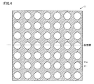
- FIG. 4 Another embodiment of the periodic structure of the present invention is shown in FIG.
- the periodic structure shown in FIG. 4 has a constricted part (notch part) 11a at one end of a circular gap.
- the entire shape of the gap 11 including the constricted portion 11a is a shape that is not mirror-symmetric with respect to a virtual plane (one of the planes orthogonal to the main surface of the periodic structure 1).
- gap part 11 has the narrow part 11a in which the gap space
- FIG. 5 Yet another embodiment of the periodic structure of the present invention is shown in FIG.
- the periodic structure shown in FIG. 5 has a slit portion (constricted portion) 11a in a part of a rectangular gap.
- the constricted portion 11a needs to be provided so as not to be mirror-symmetric with respect to the virtual plane.
- the overall shape of the gap 11 including the constricted portion 11a is a shape that is not mirror-symmetrical with respect to a virtual plane that is one of the surfaces orthogonal to the main surface of the periodic structure 1.
- gap part 11 has the narrow part 11a in which the gap space
- the constricted portion 11 a is configured so that the shape of the entire gap portion 11 is mirror-symmetric with respect to a plane perpendicular to both the virtual plane and the main surface of the periodic structure 1.
- the entire shape of the gap 11 is provided so as not to be a mirror target with respect to a plane perpendicular to both the virtual plane and the main surface of the periodic structure 1. It may be.
- the overall shape (outer shape) of the periodic structure is not limited to a square shape as shown in FIGS. 2 to 6, and any shape can be selected as long as it is a closed shape such as a rectangular shape or a circular shape. .
- gap part is not limited to one place, You may provide multiple.
- Example 1 Using 3D electromagnetic field simulation software (Micro-stripes, manufactured by CST), simulation calculation was performed on the frequency characteristics of the electromagnetic wave transmittance of the periodic structure as shown in FIG. The calculation was performed by using periodic boundary conditions for the unit structure constituting the periodic structure.
- 3D electromagnetic field simulation software Micro-stripes, manufactured by CST
- FIG. 3 is a front view showing a unit structure of the periodic structure shown in FIG.
- One main surface of the unit structure 10 was an incident surface, the opposite surface was a detection surface, and the other surfaces were periodic boundaries (dotted line portions).
- P is set to 260 ⁇ m
- D2 is set to 180 ⁇ m
- T plate thickness
- G is set to 20 ⁇ m
- L is set to 50 ⁇ m.
- the material of the periodic structure was Au.
- the unit structure was divided into unit cells whose dimensions in the XYZ directions were all 5 ⁇ m.
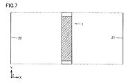
- the wave source 20 irradiates linearly polarized electromagnetic waves (plane waves) perpendicularly to the main surface of the periodic structure 1 from the wave source 20 and transmits the electromagnetic waves transmitted through the periodic structure 1. Detection is performed by the detection surface 21 provided on the opposite side.
- the case where the first electromagnetic wave (Y-polarized wave) whose deflection direction is perpendicular to the virtual plane shown in FIG. 2 (the Y-axis direction in FIGS. 3 and 7) is irradiated, and the deflection direction was calculated for each of the cases where the second electromagnetic wave (Z-polarized wave) that was parallel to the virtual plane shown in FIG. 2 (the Z-axis direction in FIGS. 3 and 7) was irradiated.
- the distance between the periodic structure 1 and the wave source 20 was 300 ⁇ m
- the distance between the periodic structure 1 and the detection surface 21 was 300 ⁇ m.
- FIG. 8 shows the frequency characteristics (transmittance spectrum) of the transmittance of the periodic structure 1 obtained by calculation.
- FIGS. 9A and 9B are electric field intensity distribution diagrams when the electromagnetic wave having the frequency in the dip waveform in the case of irradiating the Y polarized wave in FIG. 8 is shown in FIGS. 9A and 9B.
- FIGS. 9C and 9D show electric field intensity distribution diagrams when the electromagnetic wave having the frequency in FIG. 3A and 3C are views seen from the X-axis direction in FIG. 3, and FIGS. 3B and 3D are views seen from the Z-axis direction in FIG.
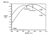
- the change in the dip waveform in FIG. 10 is shown in FIGS.
- FIG. 10 shows a case where Y-polarized light (first electromagnetic wave) is irradiated
- FIG. 11 shows a case where Z-polarized light (second electromagnetic wave) is irradiated. From these results, it is considered that measurement using the periodic structure of the present invention is possible both in the case of irradiating electromagnetic waves having two different polarization directions.
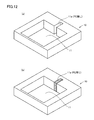
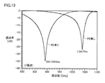
- Example 3 As for the periodic structure (periodic structure as shown in FIG. 2) similar to that of the first embodiment, as shown in FIG. 12, there is nothing in the notch (constricted portion) 11a of the gap 11 (FIG. 12 (a)) and changes in the dip waveform in the transmittance spectrum when the constricted portion 11a is filled with polyethylene are shown in FIG. FIG. 13 shows a case where Z polarization (second electromagnetic wave) is applied. Comparing the result of FIG. 13 with the result of FIG. 11, the dip waveform based on the presence of the measured object is obtained by holding the measured object only in the constricted portion when irradiating the Z polarized wave (second electromagnetic wave). It is thought that the measurement sensitivity of the measurement using the periodic structure of the present invention is improved.
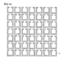
- Comparative Example 1 As a comparative example, for a periodic structure having a structure in which independent slit ring resonators 3 are periodically arranged as shown in FIG. 14, simulation calculation of frequency characteristics of electromagnetic wave transmittance is performed in the same manner as in Example 1. Went. However, in the comparative example 1, it calculated only about the case where Y polarization (1st electromagnetic wave) was irradiated.
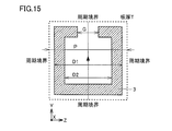
- FIG. 15 is a front view showing a unit structure of the periodic structure shown in FIG.
- One principal surface of the slit ring resonator 3 is an incident surface, and the opposite surface is a detection surface, and the periodic boundary is set as shown by a dotted line in FIG.
- G was set to 0 ⁇ m (that is, a ring resonator having no slit was subjected to simulation).
- D1 was set to 260 ⁇ m
- D2 was set to 180 ⁇ m
- T (plate thickness) was set to 60 ⁇ m
- P (pitch) was set to 280, 300, 340 and 420 ⁇ m.
- the material of the periodic structure was Au.
- the unit structure was divided into unit cells whose dimensions in the XYZ directions were all 5 ⁇ m.
- notch waveforms are generated in the passband in all pitch P waveforms compared to the transmittance spectrum in the case of irradiation with Y-polarized light in FIG.
- Example 4 In this example, the periodic structure shown in FIG. 2 was actually produced, and the transmittance spectrum was measured by terahertz time domain spectroscopy (THz-TDS).
- THz-TDS terahertz time domain spectroscopy
- a procedure for manufacturing the structure shown in FIG. 2 will be described below.
- a conductive plate having a 300 mm square smooth surface was prepared, and a photosensitive resin layer was applied and dried to a thickness of 100 ⁇ m on one surface.
- a photomask in which the periodic structure in the main surface of FIG. 2 was developed was prepared, and a portion corresponding to the gap 11 in FIG. 2 was UV cured.
- the non-cured resin component was removed by rinsing, and the conductor plate other than the portion corresponding to the gap 11 in FIG. 2 was exposed.
- An extremely thin release layer was formed on the exposed portion of the conductor plate by applying and drying a release polymer solution on the surface on which patterning by photolithography was completed.
- the conductor plate thus obtained was placed in a Ni electroplating bath and energized to form a Ni plating film with a thickness of 60 ⁇ m only on the exposed portion of the conductor plate. After plating, the cured resin remaining on the conductor plate was removed with a solvent, and the Ni-plated structure was peeled from the conductor plate to obtain a Ni plate-like periodic structure.
- the obtained periodic structure is irradiated with each of the first electromagnetic wave (Y polarized wave) and the second electromagnetic wave (Z polarized wave) in the same manner as in Example 1, and the frequency characteristics of the transmittance are shown in FIG. Measurement was performed by THz-TDS using an apparatus as shown.
- FIG. 17 shows the frequency characteristics of the transmittance when each of the first electromagnetic wave (Y polarized wave) and the second electromagnetic wave (Z polarized wave) is irradiated. From the results of FIG. 17, it can be seen that the same results as the simulation results of Example 1 shown in FIG.
- Example 5 A polyethylene film having a thickness of 10 ⁇ m was prepared as an object to be measured. The transmittance spectrum was measured in the same manner as in Example 4 with this film in close contact with one main surface of the periodic structure produced in Example 4.
- FIG. 18 shows the frequency characteristics of the transmittance when each of the first electromagnetic wave (Y polarized wave) and the second electromagnetic wave (Z polarized wave) is irradiated. From the results of FIG. 18, it can be seen that the same results as the simulation results of Example 2 shown in FIGS.
- Example 6 With respect to the periodic structure produced in Example 4, the transmittance spectrum of Z-polarized light (second electromagnetic wave) when the object to be measured was arranged only in the constricted portion 11a was measured.
- Example 4 spin-coat the surface of the periodic structure obtained in Example 4 (the constricted portion 11a is also filled with the photosensitive resin), Next, after preparing a photomask that exposes only the notch, align the periodic structure, cure the resin only in the notch, and remove the other non-exposed parts by rinsing, so that only the constricted part A sample in which the photosensitive resin remained was obtained (a state in which the photosensitive resin was filled instead of PE in FIG. 9B).
- the transmittance spectrum of Z polarization was measured in the same manner as in Example 3.
- the Z-polarized transmittance spectrum was measured in the same manner for only the periodic structure obtained in Example 4 in which no photosensitive resin was filled. The measurement results are shown in FIG.
- examples of the film to be measured such as a polyethylene film or a photosensitive resin are shown.
- biomolecules such as proteins, sugar chains, DNA, and organic / inorganic compounds are measured. It is good.
Landscapes
- Physics & Mathematics (AREA)
- Spectroscopy & Molecular Physics (AREA)
- Health & Medical Sciences (AREA)
- General Physics & Mathematics (AREA)
- Life Sciences & Earth Sciences (AREA)
- Chemical & Material Sciences (AREA)
- Analytical Chemistry (AREA)
- Biochemistry (AREA)
- General Health & Medical Sciences (AREA)
- Immunology (AREA)
- Pathology (AREA)
- Toxicology (AREA)
- Investigating Or Analysing Materials By Optical Means (AREA)
Abstract
Description
前記空隙部の形状が、前記主面と直交する面の1つである仮想面に対して鏡映対称とならない形状であり、
前記空隙部は、前記主面と前記仮想面の交線と平行な方向の幅であるギャップ間隔が部分的に狭くなった括れ部を有していることを特徴とする、周期的構造体である。
前記周期的構造体の主面に対して垂直方向に、直線偏光の電磁波を照射し、
前記周期的構造体で前方散乱または後方散乱された電磁波を検出し、
前記前方散乱された電磁波の周波数特性に生じるディップ波形、または、前記後方散乱された電磁波の周波数特性に生じるピーク波形が、前記被測定物の存在により変化することに基づいて被測定物の特性を測定する測定方法に用いられることが好ましい。
前記周期的構造体の主面に対して垂直方向に、直線偏光の電磁波を照射し、
前記周期的構造体で前方散乱または後方散乱された電磁波を検出し、
前記前方散乱された電磁波の周波数特性に生じるディップ波形、または、前記後方散乱された電磁波の周波数特性に生じるピーク波形が、前記被測定物の存在により変化することに基づいて被測定物の特性を測定することを特徴とする測定方法にも関する。
前記周期的構造体に対し、偏光方向が前記仮想面に対して平行である第2の電磁波を照射する第2のステップを含み、
前記第1のステップと前記第2のステップで、異なるモードの共振が生じることが好ましい。
s(sin i -sin θ)=nλ …(1)
と表すことができる。上記「0次方向」の0次とは、上記式(1)のnが0の場合を指す。sおよびλは0となり得ないため、n=0が成立するのは、sin i -sin θ=0の場合のみである。従って、上記「0次方向」とは、入射角と回折角が等しいとき、つまり電磁波の進行方向が変わらないような方向を意味する。
本発明の周期的構造体は、主面に垂直な方向に貫通した少なくとも2つの空隙部が、主面上の少なくとも一方向に周期的に配置された平板状の周期的構造体である。ここで、空隙部は、その全てが周期的に配置されていてもよく、本発明の効果を損なわない範囲で、一部の空隙部が周期的に配置され、他の空隙部が非周期的に配置されていてもよい。
本発明の周期的構造体の一実施形態を図2に示す。図2に示す周期的構造体は、方形の空隙の一端に括れ部(切欠部)11aを有している。本実施形態では、括れ部11aを含む空隙部11の全体形状は、周期的構造体1の主面と直交する面の1つである仮想面に対して鏡映対称とならない形状であり、かつ、空隙部11は、ギャップ間隔(上記主面と上記仮想面の交線と平行な方向の幅)が部分的に狭くなった括れ部11aを有している。
本発明の周期的構造体の別の実施形態を図4に示す。図4に示す周期的構造体は、円形の空隙の一端に括れ部(切欠部)11aを有している。本実施形態においても、括れ部11aを含む空隙部11の全体形状は、仮想面(周期的構造体1の主面と直交する面の1つ)に対して鏡映対称とならない形状であり、かつ、空隙部11は、ギャップ間隔が部分的に狭くなった括れ部11aを有している。
本発明の周期的構造体のさらに別の実施形態を図5に示す。図5に示す周期的構造体は、方形の空隙の一部にスリット部(括れ部)11aを有している。この括れ部11aは、仮想面に対して鏡映対称とならないように設けられる必要がある。本実施形態においても、括れ部11aを含む空隙部11の全体形状は、周期的構造体1の主面と直交する面の1つである仮想面に対して鏡映対称とならない形状であり、かつ、空隙部11は、ギャップ間隔が部分的に狭くなった括れ部11aを有している。
3次元電磁界シミュレーションソフト(Micro-stripes、CST社製)を用いて、図2に示すような周期的構造体の電磁波透過率の周波数特性についてのシミュレーション計算を行った。計算は、周期的構造体を構成する単位構造について、周期境界条件を用いることで行った。
実施例1と同様の周期的構造体(図2に示すような周期的構造体)について、その主面に厚み10μmポリエチレンフィルム(比誘電率=2.4)を密着させたときの透過率スペクトルにおけるディップ波形の変化を図10および図11に示す。図10はY偏波(第1の電磁波)を照射した場合、図11はZ偏波(第2の電磁波)を照射した場合を示す。これらの結果から、異なる2つの偏波方向を有する電磁波を照射した場合の双方で、本発明の周期的構造体を用いた測定が可能であると考えられる。
実施例1と同様の周期的構造体(図2に示すような周期的構造体)について、図12に示すように、その空隙部11の切欠部(括れ部)11aに何もない場合(図12(a))と、括れ部11aにポリエチレンを充填した場合での透過率スペクトルにおけるディップ波形の変化を図13に示す。図13はZ偏波(第2の電磁波)を照射した場合を示している。図13の結果を図11の結果と比較すると、Z偏波(第2の電磁波)を照射する場合において、括れ部のみに被測定物を保持することにより、被測定物の存在に基づくディップ波形の周波数シフト量が増加し、本発明の周期的構造体を用いた測定の測定感度が向上すると考えられる。
比較例として、図14に示されるような、独立したスリットリング共振器3周期的に配列された構造を有する周期的構造体について、実施例1と同様にして電磁波透過率の周波数特性のシミュレーション計算を行った。ただし、比較例1では、Y偏波(第1の電磁波)を照射した場合のみについて計算を行った。
本実施例では、図2に示す周期的構造体を実際に作製し、テラヘルツ時間領域分光法(THz-TDS)による透過率スペクトルの測定を行った。
被測定物として厚み10μmのポリエチレン製フィルムを用意した。このフィルムを、実施例4で作製した周期的構造体の一方の主面に密着させた状態で、実施例4と同様にして透過率スペクトルを測定した。
実施例4で作製した周期的構造体に対して、括れ部11aにのみ被測定物を配置した時のZ偏波(第2の電磁波)の透過率スペクトルを測定した。
Claims (7)
- 主面に垂直な方向に貫通した少なくとも2つの空隙部が、前記主面上の少なくとも一方向に周期的に配置された平板状の周期的構造体であって、
前記空隙部の形状が、前記主面と直交する面の1つである仮想面に対して鏡映対称とならない形状であり、
前記空隙部は、前記主面と前記仮想面の交線と平行な方向の幅であるギャップ間隔が部分的に狭くなった括れ部を有していることを特徴とする、周期的構造体。 - 前記周期的構造体に被測定物を保持し、
前記周期的構造体の主面に対して垂直方向に、直線偏光の電磁波を照射し、
前記周期的構造体で前方散乱または後方散乱された電磁波を検出し、
前記前方散乱された電磁波の周波数特性に生じるディップ波形、または、前記後方散乱された電磁波の周波数特性に生じるピーク波形が、前記被測定物の存在により変化することに基づいて被測定物の特性を測定する測定方法に用いられる、請求項1に記載の周期的構造体。 - 前記空隙部において、前記括れ部の両側の前記ギャップ間隔が前記括れ部よりも広くなっている、請求項1または2に記載の周期的構造体。
- 請求項1に記載の周期的構造体に被測定物を保持し、
前記周期的構造体の主面に対して垂直方向に、直線偏光の電磁波を照射し、
前記周期的構造体で前方散乱または後方散乱された電磁波を検出し、
前記前方散乱された電磁波の周波数特性に生じるディップ波形、または、前記後方散乱された電磁波の周波数特性に生じるピーク波形が、前記被測定物の存在により変化することに基づいて被測定物の特性を測定することを特徴とする測定方法。 - 前記周期的構造体に対し、偏光方向が前記仮想面に対して垂直である第1の電磁波を照射する第1のステップ、および/または、
前記周期的構造体に対し、偏光方向が前記仮想面に対して平行である第2の電磁波を照射する第2のステップを含み、
前記第1のステップと前記第2のステップで、異なるモードの共振が生じる、請求項4に記載の測定方法。 - 前記第1のステップにより生じる共振がTE11モード様共振であり、前記第2のステップにより生じる共振がLC共振である、請求項5に記載の測定方法。
- 前記第2のステップにより生じる共振に基づく前記ディップ波形または前記ピーク波形の周波数が、前記第1のステップにより生じる共振に基づく前記ディップ波形または前記ピーク波形の周波数の1/10~10倍になるように、前記括れ部の前記主面と前記仮想面の交線と平行な方向の幅が調節されている、請求項5または6に記載の測定方法。
Priority Applications (2)
| Application Number | Priority Date | Filing Date | Title |
|---|---|---|---|
| EP12850549.2A EP2781908A4 (en) | 2011-11-18 | 2012-08-17 | PERIODIC STRUCTURE AND MEASURING METHOD EMPLOYING IT |
| US14/278,593 US20140247452A1 (en) | 2011-11-18 | 2014-05-15 | Periodic structure and measurement method using the same |
Applications Claiming Priority (2)
| Application Number | Priority Date | Filing Date | Title |
|---|---|---|---|
| JP2011-252405 | 2011-11-18 | ||
| JP2011252405 | 2011-11-18 |
Related Child Applications (1)
| Application Number | Title | Priority Date | Filing Date |
|---|---|---|---|
| US14/278,593 Continuation US20140247452A1 (en) | 2011-11-18 | 2014-05-15 | Periodic structure and measurement method using the same |
Publications (1)
| Publication Number | Publication Date |
|---|---|
| WO2013073242A1 true WO2013073242A1 (ja) | 2013-05-23 |
Family
ID=48429323
Family Applications (1)
| Application Number | Title | Priority Date | Filing Date |
|---|---|---|---|
| PCT/JP2012/070878 Ceased WO2013073242A1 (ja) | 2011-11-18 | 2012-08-17 | 周期的構造体、および、それを用いた測定方法 |
Country Status (4)
| Country | Link |
|---|---|
| US (1) | US20140247452A1 (ja) |
| EP (1) | EP2781908A4 (ja) |
| JP (1) | JPWO2013073242A1 (ja) |
| WO (1) | WO2013073242A1 (ja) |
Cited By (1)
| Publication number | Priority date | Publication date | Assignee | Title |
|---|---|---|---|---|
| JP2019060841A (ja) * | 2017-09-22 | 2019-04-18 | グローリー株式会社 | 電磁波センサ、電磁波検出装置、媒体処理装置及び媒体検査装置 |
Families Citing this family (3)
| Publication number | Priority date | Publication date | Assignee | Title |
|---|---|---|---|---|
| JP6938291B2 (ja) * | 2017-09-08 | 2021-09-22 | 東芝テック株式会社 | センサ、検出装置及び検出システム |
| JP7208032B2 (ja) * | 2019-01-28 | 2023-01-18 | キヤノン株式会社 | 半導体装置 |
| JP7314026B2 (ja) * | 2019-11-14 | 2023-07-25 | 東芝テック株式会社 | 検出装置及び基板 |
Citations (4)
| Publication number | Priority date | Publication date | Assignee | Title |
|---|---|---|---|---|
| WO2011027642A1 (ja) | 2009-09-03 | 2011-03-10 | 株式会社村田製作所 | 被測定物の特性を測定する方法、および平板状の周期的構造体 |
| JP2011515688A (ja) * | 2008-03-28 | 2011-05-19 | ドリッテ パテントポートフォーリオ ベタイリグングスゲゼルシャフト ミット ベシュレンクテル ハフツング ウント コンパニー コマンディートゲゼルシャフト | 表面センサの製造方法、表面センサシステムおよび表面センサの使用 |
| WO2011077949A1 (ja) * | 2009-12-22 | 2011-06-30 | 株式会社村田製作所 | 被測定物の特性を測定する方法および測定装置 |
| WO2011142155A1 (ja) * | 2010-05-12 | 2011-11-17 | 株式会社村田製作所 | 被測定物の特性を測定する方法、それに用いられる空隙配置構造体および測定装置 |
Family Cites Families (1)
| Publication number | Priority date | Publication date | Assignee | Title |
|---|---|---|---|---|
| JP4911965B2 (ja) * | 2005-12-09 | 2012-04-04 | 株式会社アドバンテスト | 測定用構造体、測定装置、方法およびプログラム |
-
2012
- 2012-08-17 WO PCT/JP2012/070878 patent/WO2013073242A1/ja not_active Ceased
- 2012-08-17 EP EP12850549.2A patent/EP2781908A4/en not_active Withdrawn
- 2012-08-17 JP JP2013544155A patent/JPWO2013073242A1/ja active Pending
-
2014
- 2014-05-15 US US14/278,593 patent/US20140247452A1/en not_active Abandoned
Patent Citations (4)
| Publication number | Priority date | Publication date | Assignee | Title |
|---|---|---|---|---|
| JP2011515688A (ja) * | 2008-03-28 | 2011-05-19 | ドリッテ パテントポートフォーリオ ベタイリグングスゲゼルシャフト ミット ベシュレンクテル ハフツング ウント コンパニー コマンディートゲゼルシャフト | 表面センサの製造方法、表面センサシステムおよび表面センサの使用 |
| WO2011027642A1 (ja) | 2009-09-03 | 2011-03-10 | 株式会社村田製作所 | 被測定物の特性を測定する方法、および平板状の周期的構造体 |
| WO2011077949A1 (ja) * | 2009-12-22 | 2011-06-30 | 株式会社村田製作所 | 被測定物の特性を測定する方法および測定装置 |
| WO2011142155A1 (ja) * | 2010-05-12 | 2011-11-17 | 株式会社村田製作所 | 被測定物の特性を測定する方法、それに用いられる空隙配置構造体および測定装置 |
Non-Patent Citations (5)
| Title |
|---|
| DAI OHNISHI ET AL.: "Optical properties of gold nano-slit-rings with plasmonic resonance frequencies in terahertz region", NANOTECH JAPAN, FOCUS 26 <11-TH> OPTICAL PROPERTIES OF GOLD NANO-SLIT RINGS, vol. 3, no. 5, 8 October 2010 (2010-10-08) |
| DAI OHNISHI ET AL.: "Optical properties of gold nano-slit-rings with plasmonic resonance frequencies in terahertz region", NANOTECH JAPAN, FOCUS 26 <11-TH> OPTICAL PROPERTIES OF GOLD NANO-SLIT-RINGS, vol. 3, no. 5, 8 October 2010 (2010-10-08) |
| GADOT F ET AL.: "Infrared response of a metamaterial made of gold wires and split ring resonators deposited on silicon", OPTICAL AND QUANTUM ELECTRONICS, vol. 39, no. 4/6, 3 July 2007 (2007-07-03), pages 273 - 284, XP019532406 * |
| See also references of EP2781908A4 |
| SINGH R ET AL.: "Random terahertz metamaterials", JOURNAL OF OPTICS, vol. 12, no. 1, January 2010 (2010-01-01), pages 015101, XP020170915 * |
Cited By (2)
| Publication number | Priority date | Publication date | Assignee | Title |
|---|---|---|---|---|
| JP2019060841A (ja) * | 2017-09-22 | 2019-04-18 | グローリー株式会社 | 電磁波センサ、電磁波検出装置、媒体処理装置及び媒体検査装置 |
| JP7181700B2 (ja) | 2017-09-22 | 2022-12-01 | グローリー株式会社 | 電磁波検出装置、媒体処理装置及び媒体検査装置 |
Also Published As
| Publication number | Publication date |
|---|---|
| EP2781908A4 (en) | 2015-07-08 |
| EP2781908A1 (en) | 2014-09-24 |
| US20140247452A1 (en) | 2014-09-04 |
| JPWO2013073242A1 (ja) | 2015-04-02 |
Similar Documents
| Publication | Publication Date | Title |
|---|---|---|
| JP5582192B2 (ja) | 被測定物の特性を測定する方法 | |
| JP5761416B2 (ja) | 平板状の周期的構造体 | |
| JP5609654B2 (ja) | 被測定物の測定方法 | |
| JP5914474B2 (ja) | 被測定物の測定方法 | |
| WO2013073242A1 (ja) | 周期的構造体、および、それを用いた測定方法 | |
| JP5418721B2 (ja) | 測定構造体、その製造方法、および、それを用いた測定方法 | |
| JP5828899B2 (ja) | 測定用デバイス、および、それを用いた被測定物の特性測定方法 | |
| JP5991426B2 (ja) | 空隙配置構造体およびそれを用いた測定方法 | |
| WO2011013452A1 (ja) | 被測定物の特性を測定する方法、測定装置およびフィルタ装置 | |
| JP5967201B2 (ja) | 空隙配置構造体およびそれを用いた測定方法 | |
| JPWO2011142155A1 (ja) | 被測定物の特性を測定する方法、それに用いられる空隙配置構造体および測定装置 | |
| JP5384648B2 (ja) | 被測定物の特性を測定する方法 | |
| WO2014132692A1 (ja) | 測定デバイスおよびその製造方法 | |
| JP2013024639A (ja) | 被測定物の測定方法 |
Legal Events
| Date | Code | Title | Description |
|---|---|---|---|
| 121 | Ep: the epo has been informed by wipo that ep was designated in this application |
Ref document number: 12850549 Country of ref document: EP Kind code of ref document: A1 |
|
| REEP | Request for entry into the european phase |
Ref document number: 2012850549 Country of ref document: EP |
|
| WWE | Wipo information: entry into national phase |
Ref document number: 2012850549 Country of ref document: EP |
|
| ENP | Entry into the national phase |
Ref document number: 2013544155 Country of ref document: JP Kind code of ref document: A |
|
| NENP | Non-entry into the national phase |
Ref country code: DE |