WO2013084589A1 - 半導体装置および半導体装置製造方法 - Google Patents
半導体装置および半導体装置製造方法 Download PDFInfo
- Publication number
- WO2013084589A1 WO2013084589A1 PCT/JP2012/076452 JP2012076452W WO2013084589A1 WO 2013084589 A1 WO2013084589 A1 WO 2013084589A1 JP 2012076452 W JP2012076452 W JP 2012076452W WO 2013084589 A1 WO2013084589 A1 WO 2013084589A1
- Authority
- WO
- WIPO (PCT)
- Prior art keywords
- metal
- semiconductor device
- bus bar
- outer case
- circuit board
- Prior art date
- Legal status (The legal status is an assumption and is not a legal conclusion. Google has not performed a legal analysis and makes no representation as to the accuracy of the status listed.)
- Ceased
Links
Images


Classifications
-
- H—ELECTRICITY
- H02—GENERATION; CONVERSION OR DISTRIBUTION OF ELECTRIC POWER
- H02M—APPARATUS FOR CONVERSION BETWEEN AC AND AC, BETWEEN AC AND DC, OR BETWEEN DC AND DC, AND FOR USE WITH MAINS OR SIMILAR POWER SUPPLY SYSTEMS; CONVERSION OF DC OR AC INPUT POWER INTO SURGE OUTPUT POWER; CONTROL OR REGULATION THEREOF
- H02M7/00—Conversion of AC power input into DC power output; Conversion of DC power input into AC power output
- H02M7/003—Constructional details, e.g. physical layout, assembly, wiring or busbar connections
-
- H—ELECTRICITY
- H05—ELECTRIC TECHNIQUES NOT OTHERWISE PROVIDED FOR
- H05K—PRINTED CIRCUITS; CASINGS OR CONSTRUCTIONAL DETAILS OF ELECTRIC APPARATUS; MANUFACTURE OF ASSEMBLAGES OF ELECTRICAL COMPONENTS
- H05K13/00—Apparatus or processes specially adapted for manufacturing or adjusting assemblages of electric components
-
- H—ELECTRICITY
- H05—ELECTRIC TECHNIQUES NOT OTHERWISE PROVIDED FOR
- H05K—PRINTED CIRCUITS; CASINGS OR CONSTRUCTIONAL DETAILS OF ELECTRIC APPARATUS; MANUFACTURE OF ASSEMBLAGES OF ELECTRICAL COMPONENTS
- H05K7/00—Constructional details common to different types of electric apparatus
- H05K7/14—Mounting supporting structure in casing or on frame or rack
- H05K7/1422—Printed circuit boards receptacles, e.g. stacked structures, electronic circuit modules or box like frames
- H05K7/1427—Housings
- H05K7/1432—Housings specially adapted for power drive units or power converters
- H05K7/14322—Housings specially adapted for power drive units or power converters wherein the control and power circuits of a power converter are arranged within the same casing
-
- H—ELECTRICITY
- H10—SEMICONDUCTOR DEVICES; ELECTRIC SOLID-STATE DEVICES NOT OTHERWISE PROVIDED FOR
- H10W—GENERIC PACKAGES, INTERCONNECTIONS, CONNECTORS OR OTHER CONSTRUCTIONAL DETAILS OF DEVICES COVERED BY CLASS H10
- H10W40/00—Arrangements for thermal protection or thermal control
- H10W40/10—Arrangements for heating
-
- H—ELECTRICITY
- H10—SEMICONDUCTOR DEVICES; ELECTRIC SOLID-STATE DEVICES NOT OTHERWISE PROVIDED FOR
- H10W—GENERIC PACKAGES, INTERCONNECTIONS, CONNECTORS OR OTHER CONSTRUCTIONAL DETAILS OF DEVICES COVERED BY CLASS H10
- H10W40/00—Arrangements for thermal protection or thermal control
- H10W40/60—Securing means for detachable heating or cooling arrangements, e.g. clamps
- H10W40/611—Bolts or screws
-
- H—ELECTRICITY
- H10—SEMICONDUCTOR DEVICES; ELECTRIC SOLID-STATE DEVICES NOT OTHERWISE PROVIDED FOR
- H10W—GENERIC PACKAGES, INTERCONNECTIONS, CONNECTORS OR OTHER CONSTRUCTIONAL DETAILS OF DEVICES COVERED BY CLASS H10
- H10W42/00—Arrangements for protection of devices
-
- H—ELECTRICITY
- H10—SEMICONDUCTOR DEVICES; ELECTRIC SOLID-STATE DEVICES NOT OTHERWISE PROVIDED FOR
- H10W—GENERIC PACKAGES, INTERCONNECTIONS, CONNECTORS OR OTHER CONSTRUCTIONAL DETAILS OF DEVICES COVERED BY CLASS H10
- H10W72/00—Interconnections or connectors in packages
-
- H—ELECTRICITY
- H10—SEMICONDUCTOR DEVICES; ELECTRIC SOLID-STATE DEVICES NOT OTHERWISE PROVIDED FOR
- H10W—GENERIC PACKAGES, INTERCONNECTIONS, CONNECTORS OR OTHER CONSTRUCTIONAL DETAILS OF DEVICES COVERED BY CLASS H10
- H10W76/00—Containers; Fillings or auxiliary members therefor; Seals
- H10W76/10—Containers or parts thereof
-
- H—ELECTRICITY
- H10—SEMICONDUCTOR DEVICES; ELECTRIC SOLID-STATE DEVICES NOT OTHERWISE PROVIDED FOR
- H10W—GENERIC PACKAGES, INTERCONNECTIONS, CONNECTORS OR OTHER CONSTRUCTIONAL DETAILS OF DEVICES COVERED BY CLASS H10
- H10W90/00—Package configurations
-
- H—ELECTRICITY
- H10—SEMICONDUCTOR DEVICES; ELECTRIC SOLID-STATE DEVICES NOT OTHERWISE PROVIDED FOR
- H10W—GENERIC PACKAGES, INTERCONNECTIONS, CONNECTORS OR OTHER CONSTRUCTIONAL DETAILS OF DEVICES COVERED BY CLASS H10
- H10W40/00—Arrangements for thermal protection or thermal control
- H10W40/20—Arrangements for cooling
- H10W40/25—Arrangements for cooling characterised by their materials
- H10W40/255—Arrangements for cooling characterised by their materials having a laminate or multilayered structure, e.g. direct bond copper [DBC] ceramic substrates
-
- H—ELECTRICITY
- H10—SEMICONDUCTOR DEVICES; ELECTRIC SOLID-STATE DEVICES NOT OTHERWISE PROVIDED FOR
- H10W—GENERIC PACKAGES, INTERCONNECTIONS, CONNECTORS OR OTHER CONSTRUCTIONAL DETAILS OF DEVICES COVERED BY CLASS H10
- H10W40/00—Arrangements for thermal protection or thermal control
- H10W40/40—Arrangements for thermal protection or thermal control involving heat exchange by flowing fluids
- H10W40/47—Arrangements for thermal protection or thermal control involving heat exchange by flowing fluids by flowing liquids, e.g. forced water cooling
-
- H—ELECTRICITY
- H10—SEMICONDUCTOR DEVICES; ELECTRIC SOLID-STATE DEVICES NOT OTHERWISE PROVIDED FOR
- H10W—GENERIC PACKAGES, INTERCONNECTIONS, CONNECTORS OR OTHER CONSTRUCTIONAL DETAILS OF DEVICES COVERED BY CLASS H10
- H10W76/00—Containers; Fillings or auxiliary members therefor; Seals
- H10W76/10—Containers or parts thereof
- H10W76/12—Containers or parts thereof characterised by their shape
- H10W76/13—Containers comprising a conductive base serving as an interconnection
- H10W76/136—Containers comprising a conductive base serving as an interconnection having other interconnections perpendicular to the conductive base
-
- H—ELECTRICITY
- H10—SEMICONDUCTOR DEVICES; ELECTRIC SOLID-STATE DEVICES NOT OTHERWISE PROVIDED FOR
- H10W—GENERIC PACKAGES, INTERCONNECTIONS, CONNECTORS OR OTHER CONSTRUCTIONAL DETAILS OF DEVICES COVERED BY CLASS H10
- H10W90/00—Package configurations
- H10W90/701—Package configurations characterised by the relative positions of pads or connectors relative to package parts
- H10W90/751—Package configurations characterised by the relative positions of pads or connectors relative to package parts of bond wires
- H10W90/753—Package configurations characterised by the relative positions of pads or connectors relative to package parts of bond wires between laterally-adjacent chips
Definitions
- the present invention relates to a semiconductor device having a semiconductor element such as a power semiconductor element (IGBT: Insulated Gate Bipolar Transistor) and a semiconductor device manufacturing method for manufacturing the semiconductor device.
- a semiconductor element such as a power semiconductor element (IGBT: Insulated Gate Bipolar Transistor)
- IGBT Insulated Gate Bipolar Transistor
- IPM Intelligent Power Module
- the IPM is a power module in which a drive circuit and a control circuit for a power device such as a power MOSFET (Metal Oxide Semiconductor Field Effect Transistor) for power control and an IGBT are incorporated.
- IPM is used in a wide range of fields as being useful for reducing the size and weight of devices, reducing development costs, and shortening the development period.
- Patent Document 2 a semiconductor device has been proposed in which the upper part of the columnar block is protruded from the upper surface of the resin case, and external parts are supported by a screw seat and fixed to the screw seat by a fastening screw.
- the semiconductor device includes an outer case in which a semiconductor element is housed, a circuit board on which a control circuit is mounted, and a metal component.
- the metal part includes a first attachment portion, a second attachment portion, and a bus bar.
- the first attachment portion attaches the circuit board to the outer case, and is connected to the ground pattern of the circuit board at the time of attachment.
- the second attachment portion attaches an external device to the outer case and is grounded at the time of attachment.
- the bus bar connects the first attachment portion and the second attachment portion.
- the semiconductor device includes a first attachment portion that attaches a circuit board to an outer case and connects to a ground pattern of the circuit board, a second attachment portion that attaches an external device to the outer case and grounds, and first and first It was set as the structure provided with the metal component containing the bus bar which connects 2 attachment parts mutually. As a result, it is possible to improve the noise resistance performance by eliminating the need to review the circuit configuration and increase the number of retrofitted components.
- the semiconductor device manufacturing method when the circuit board is fastened and fixed to the metal support provided in the outer case with screws, the ground pattern of the circuit board is connected to the metal support. Further, when the external device is fastened and fixed to the ring portion provided in the outer case with a screw, the protruding portion of the screw protruding to the outside from the outer case is grounded. And it decided to manufacture a semiconductor device by connecting a metal support
- FIG. 7 is a partial cross-sectional view showing the main part of the semiconductor device when FIG. 6 is viewed from the B direction. It is a figure which shows the structure of a metal component. It is a figure which shows the other structure of a metal component. It is a figure which shows the other structure of a metal component. It is a figure which shows the other structure of a metal component. It is a figure which shows the other structure of a metal component. It is a figure which shows the flowchart of the semiconductor device manufacturing method which concerns on embodiment of this invention.
- FIG. 1 is a diagram illustrating a configuration example of a semiconductor device according to an embodiment of the present invention.
- the semiconductor device 1 includes a circuit board 10, an enclosing case 20, and a metal component 30, and corresponds to, for example, an IPM module.
- a control circuit 11 is mounted on the surface of the circuit board 10.
- the outer case 20 is a resin case in which the semiconductor element 23 is housed.
- the metal component 30 is included in the outer case 20 and includes a first attachment portion 31a, a second attachment portion 32a, and a bus bar 33a.
- the first attachment portion 31a is provided to attach the circuit board 10 to the outer case 20 and to connect with a ground pattern (hereinafter referred to as a GND pattern) of the circuit board 10 at the time of attachment.
- the second mounting portion 32a is provided to attach the external device 4 to the outer case 20 and to be grounded at the time of mounting.
- Examples of the external device 4 include cooling fins and other device housings.
- the bus bar 33a connects the first attachment portion 31a and the second attachment portion 32a.
- the semiconductor device 1 has the circuit board 10 attached to the outer case 20, the first attachment portion 31 a connected to the GND pattern of the circuit board 10, and the external device 4 attached to the outer case 20.
- the metal part 30 includes a second attachment portion 32a that is grounded at the time of attachment, and a bus bar 33a that connects the first attachment portion 31a and the second attachment portion 32a.
- the GND pattern of the circuit board 10 is electrically connected to the grounded second mounting portion 32a. Therefore, noise generated on the circuit board 10 or noise that has entered the circuit board 10 can be efficiently released from the grounding location.
- FIG. 2 is a plan view of the IPM module
- FIG. 3 is a cross-sectional view of the IPM module when FIG. 2 is viewed from the A direction.
- the IPM module 2 includes a circuit board 100 and an enclosing case 200.
- a heat radiating base plate 210 is positioned on the bottom surface of the outer case 200, and cooling fins 40 for cooling the heat radiating base plate 210 are provided on the lower surface side of the heat radiating base plate 210.
- An insulating substrate 220 on which a circuit pattern or a conductive material is laid is mounted on the upper surface of the heat dissipation base plate 210, and a semiconductor element such as an IGBT 23 is mounted on the insulating substrate 220 (mounting of IGBT or the like). The part will be described later with reference to FIG. 4).
- the resin outer case 200 is provided with an open screw seat 301 for attaching the circuit board 100.
- the circuit board 100 is fastened and fixed to the screw seat 301 by screws a1 to a4 at the four corners, and is attached to the upper surface of the outer casing 200 (in FIG. 3, the screws a1 and a2 are fastened to the screw seat 301). Is shown).
- control circuits 101-1 to 101-6 composed of circuit elements such as an IC (Integrated Circuit), an LSI (Large Scale Integration), a transistor, a resistor, and a capacitor are mounted. Yes.
- a connector 120 into which an external connection cable is inserted and control terminals 102-1 to 102-8 are mounted on the surface of the circuit board 100.
- the control terminals 102-1 to 102-8 connect the gate line of the IGBT 23 housed in the outer case 200 and the control circuits 101-1 to 101-6, and the control terminals 101-1 to 101-6 It is a relay terminal that performs switching control of the IGBT 23 according to the transmitted control signal.
- a main terminal (U) 201-1, a main terminal (V) 201-2, and a main terminal (W) 201-3 are provided on one side of the frame portion of the outer casing 200, and the other side of the frame portion.
- the main terminal (U) 201-1, main terminal (V) 201-2, and main terminal (W) 201-3 are terminals for driving an external motor by switching control of the IGBT 23.
- the power supply terminal (P) 202-1 and the power supply terminal (N) 202-2 are terminals to which power is supplied from the outside.
- openings 250-1 to 250-4 are provided at the four corners of the frame of the outer case 200, and screws b1 to b4 are respectively inserted into the openings 250-1 to 250-4 and fastened.
- the outer casing 200 and the cooling fin 40 are connected.
- a ring portion 302 is provided inside the frame portion of the outer case 200.
- the ring portion 302 connects the outer case 200 and the heat radiating base plate 210. Then, the screws b1 to b4 are inserted into the ring portion 302, and the outer case 200 and the cooling fin 40 are fastened and fixed with the heat dissipation base plate 210 interposed therebetween (in FIG. 3, provided in the opening 250-1). Only the fastening part of the ring part 302 is shown).
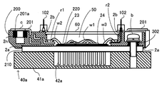
- FIG. 4 is a cross-sectional view of the outer case and the cooling fin. The structure inside the outer casing 200 in a state where the circuit board 100 is not attached to the outer casing 200 and the inner structure of the water-cooled cooling fin 40a are shown.
- a heat radiating base plate 210 On the bottom surface of the enclosing case 200, a heat radiating base plate 210 that is fixed to the opening step surface 2a with an adhesive and closes the opening is provided.
- An insulating substrate 220 on which a circuit pattern or a conductive material is laid is mounted on the upper surface of the heat dissipation base plate 210.
- the insulating substrate 220 is mounted with a chip such as an IGBT 23 or a FWD 24 (Free Wheeling Diode) that is a diode for commutating a load current.
- the plurality of IGBTs 23 and the FWD 24 are connected to each other by bonding wires w1.
- lead terminals r1 and r2 are embedded in the frame portion of the outer casing 200 by insert molding, and are connected to the IGBT 23 by bonding wires w2 and w3.
- the data line of the IGBT 23 is connected to the lead terminal r1 through the bonding wire w2, and the lead terminal r1 is connected to the main terminal 201 for driving the motor.
- the gate line of the IGBT 23 is connected to the lead terminal r2 through the bonding wire w3, and the lead terminal r2 is connected to the control terminal 102.
- the main terminal 201 is provided with an opening hole 201a.
- the screw c is inserted into the opening hole 201a and fastened to the nut 2n formed in the outer case 200, so that the main terminal 201 is installed on the surface of the outer case 200 in a bent state. .
- the internal space of the outer case 200 is filled with a sealing material 50 of gel resin (for example, silicone resin). Further, the opening step surface 2b of the outer case 200 is fixed with an adhesive, and the opening portion is closed with a cover plate 60 made of insulating resin.
- a sealing material 50 of gel resin for example, silicone resin
- a screw b is inserted into the ring portion 302 that is insert-molded in the frame portion of the outer case 200, and the outer case 200 and the cooling fin 40a are fastened and fixed.
- the cooling fin 40a is a water-cooling type cooling fin, and in the case of the water-cooling type, a plurality of fins 42a are provided in the water jacket 41a.
- the cooling fins 40a shown above are water-cooled, but may be air-cooled.
- Fig. 5 shows the configuration of the cooling fins.
- (A) is a water-cooling type cooling fin 40a
- (b) is an air-cooling type cooling fin 40b.
- the fin 42b has a structure that directly contacts the air.
- the cooling fin attached to the outer case 200 may be either water-cooled or air-cooled.
- noise countermeasure pattern design is performed. Or adding noise countermeasure parts such as bypass capacitors and shield plates.
- the present technology has been made in view of the above points, and provides a semiconductor device and a semiconductor device manufacturing method that improve noise resistance performance without requiring a review of the circuit configuration and an increase in retrofitted components.
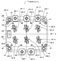
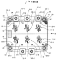
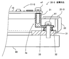
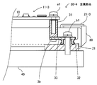
- FIG. 6 is a plan view of the semiconductor device according to the embodiment of the present invention
- FIG. 7 is a partial cross-sectional view showing the main part of the semiconductor device when FIG. 6 is viewed from the B direction.
- the semiconductor device 1 a includes a circuit board 10 and an enclosing case 20.
- a heat radiating base plate 21 is positioned on the bottom surface of the outer casing 20, and a cooling fin 40 (water-cooled type or air-cooled type) for cooling the heat radiating base plate 21 is provided on the lower surface side of the heat radiating base plate 21. May be provided).
- An insulating substrate 22 on which a circuit pattern or a conductive material is laid is mounted on the upper surface of the heat dissipation base plate 21, and a semiconductor element such as an IGBT 23 is mounted on the insulating substrate 22 (a semiconductor such as an IGBT).
- the element mounting portion has the same basic configuration as that of FIG.
- the resin surrounding case 20 is provided with a metal support 31 for mounting the circuit board 10.
- the circuit board 10 is attached to the upper surface of the surrounding case 20 by fastening the four corners to the metal support 31 with screws a1 to a4 (corresponding to the first screw) (in FIG. 7, in the metal support 31). On the other hand, the state where the screws a1 and a2 are fastened is shown).
- control circuits 11-1 to 11-6 each including circuit elements such as an IC, an LSI, a transistor, a resistor, and a capacitor are mounted. Further, a connector 12 into which an external connection cable is inserted and control terminals 12-1 to 12-8 are mounted on the surface of the circuit board 10.
- the control terminals 12-1 to 12-8 connect the gate line of the IGBT 23 built in the outer casing 20 to the control circuits 11-1 to 11-6, and are connected to the control circuits 11-1 to 11-6. It is a relay terminal that performs switching control of the IGBT 23 according to the transmitted control signal.
- a main terminal (U) 21-1, a main terminal (V) 21-2, and a main terminal (W) 21-3 are provided on one side of the frame portion of the surrounding case 20, and the other side of the frame portion is provided.
- a power supply terminal (P) 22-1 and a power supply terminal (N) 22-2 are provided.
- the main terminal (U) 21-1, main terminal (V) 21-2, and main terminal (W) 21-3 are terminals for driving an external motor by switching control of the IGBT 23.
- the power supply terminal (P) 22-1 and the power supply terminal (N) 22-2 are terminals to which power is supplied from the outside.
- openings 25-1 to 25-4 are provided at the four corners of the frame of the outer case 20, and screws b1 to b4 (corresponding to the second screw) are provided in the openings 25-1 to 25-4.
- the outer case 20 and the cooling fin 40 are fastened and fixed by being inserted and fastened (FIG. 7 shows only the fastened portion of the ring portion 32 provided in the opening 25-1). .
- the metal part 30 is provided at one location on the upper right opening 25-1 among the four corners of the frame of the outer case 20.
- the metal parts 30 may be provided in any of the other openings 25-2 to 25-4, or the metal parts 30 may be provided not only in one place but also in a plurality of places. Good.
- the metal component 30 includes a metal column 31, a ring portion 32, and a metal bus bar 33.
- the metal support 31 serves as a screw seat for fastening and fixing the circuit board 10 to the outer case 20 with the screw a1.
- the screw a1 is inserted into the metal support 31 and the circuit board 10 is fastened and fixed to the outer case 20.
- the metal support 31 is connected to the GND pattern on the back surface of the circuit board 10 when the circuit board 10 is attached to the outer case 20.
- the ring portion 32 connects the heat radiating base plate 21 included in the outer case 20 and the outer case 20.
- the ring portion 32 serves as a screw seat for fastening and fixing the cooling fin 40 to the outer case 20 with the screw b1.
- the screw b1 is inserted into the ring portion 32, and the cooling fin 40 is inserted into the outer case 20. Fastened and fixed.
- the ring portion 32 is grounded through a screw b1 protruding outside the outer case 20.
- the metal bus bar 33 connects the metal column 31 and the ring portion 32.
- the screw b1 protruding outside the outer case 20 fastens and fixes the outer case 20 and the cooling fin 40, the protruding portion of the screw b1 from the outer case 20 is not attached to the cooling fin 40.
- the GND pattern of the circuit board 10 is connected to the metal support 31, the ring part 32 is connected to the metal surface of the cooling fin 40 via the screw b 1, and the metal bus bar 33 is connected to the metal support 31 and the ring part. 32 is connected.
- the GND pattern of the circuit board 10 is electrically connected to the metal surface of the cooling fin 40 via the metal column 31, the metal bus bar 33, and the ring portion 32. Since the metal surface of the cooling fin 40 is grounded to the reference ground plane, the GND pattern of the circuit board 10 is grounded to the reference ground plane through the metal surface of the cooling fin 40.
- an insulator such as a silicon compound may be inserted between the heat dissipation base plate 21 and the cooling fin 40 to enhance the cooling effect.
- the contact surfaces of the heat radiating base plate 21 and the cooling fin 40 are electrically insulated.
- the outer casing 20 and the cooling fin 40 are fixedly installed by inserting the screw b1 into the metal of the cooling fin 40 and sandwiching the heat dissipation base plate 21. Therefore, the metal component 30 is electrically connected via the screw b1 and is not insulated by silicon compound or the like.
- the semiconductor device 1a there is no problem even if an insulator such as a silicon compound is inserted between the heat dissipation base plate 21 and the cooling fin 40. Therefore, also in the semiconductor device 1a, it is possible to increase the thermal conductivity and increase the cooling effect by inserting an insulator such as a silicon compound so that the heat radiating base plate 21 and the cooling fin 40 are more closely attached. is there.
- the external device 4 is the cooling fin 40, but the external device 4 may be a casing of another device.
- the outer casing 20 and the casing are fastened and fixed by the screw b1 protruding to the outside of the outer casing 20, so that the GND pattern of the circuit board 10 is connected to the metal of the casing via the metal component 30. It is electrically connected to the surface, and the same effect as described above can be obtained.
- FIG. 8 is a diagram showing the configuration of the metal part.
- the metal part 30-1 includes three parts including a metal column 31, a ring part 32, and a metal bus bar 33.
- One end of the metal bus bar 33 is fixed to a protrusion provided at the tip of the metal column 31.
- the other end of the metal bus bar 33 is fastened and fixed to the ring portion 32 with a screw b1.
- one end of the metal bus bar 33 is fixed to the protrusion provided at the tip of the metal column 31, but other connection methods may be used.
- the recess of the metal support 31 and the metal bus bar 33 can be fitted together, or the hole diameter of the metal bus bar 33 can be expanded to fit the body of the metal support 31.
- the screw a ⁇ b> 1 may be penetrated from the bottom surface of the metal column 31, and one end of the metal bus bar 33 may be fixed to the metal column 31 at the portion of the screw a ⁇ b> 1 that has penetrated.
- a metal part 30-2 shown in FIG. 9 is a single part in which the metal column 31, the ring portion 32, and the metal bus bar 33 are integrally molded. Thus, the structure by which each component is integrally molded may be sufficient.
- the metal part 30-3 shown in FIG. 10 includes a part 3a in which a metal column 31 and a metal bus bar 33 are integrally molded, and a ring portion 32.
- a metal bus bar 33 of the component 3a is fastened and fixed to the ring portion 32 with a screw b1.
- the metal part 30-4 shown in FIG. 11 includes a part 3 b in which the ring portion 32 and the metal bus bar 33 are integrally molded, and a metal column 31.
- one end of the metal bus bar 33 of the component 3b is fastened and fixed to the metal column 31 with a screw a1.
- the metal part 30 may be formed of either a part in which the metal column 31 and the metal bus bar 33 are integrally molded or a part in which the ring part 32 and the metal bus bar 33 are integrally molded.
- the metal component 30 is fixed to the outer case 20 by integral molding such as insert molding.
- FIG. 12 is a flowchart of the semiconductor device manufacturing method according to the embodiment of the present invention.
- the semiconductor device 1 has the first mounting portion that attaches the circuit board to the outer case and connects to the ground pattern of the circuit board, and the second attachment that attaches the external device to the outer case and grounds it. And a metal part including a bus bar that connects the first and second attachment portions to each other.
- the GND pattern of the circuit board is connected to the reference GND (reference ground plane) through a metal part at the shortest distance, it is possible to significantly reduce the wiring inductor and improve the noise resistance performance. . Furthermore, it is possible to cope with a noise signal durability test up to a high frequency band.
- the semiconductor device manufacturing method when the circuit board is fastened and fixed to the metal support provided in the outer case with screws, the ground pattern of the circuit board is connected to the metal support.
- an external device when fastened and fixed to the ring portion provided in the outer case with a screw, the screw protrudes to the outside and is grounded. And it decided to manufacture a semiconductor device by connecting a metal support
Landscapes
- Engineering & Computer Science (AREA)
- Microelectronics & Electronic Packaging (AREA)
- Power Engineering (AREA)
- Manufacturing & Machinery (AREA)
- Cooling Or The Like Of Electrical Apparatus (AREA)
- Chemical & Material Sciences (AREA)
- Materials Engineering (AREA)
- Shielding Devices Or Components To Electric Or Magnetic Fields (AREA)
Abstract
耐ノイズ性能の向上を図る。 半導体装置(1)は、回路基板(10)、外囲ケース(20)および金属部品(30)を備える。回路基板(10)の表面には、制御回路(11)が実装されている。外囲ケース(20)は、半導体素子(23)を内装している樹脂製のケースである。金属部品(30)は、外囲ケース(20)内部に含まれ、第1の取付部(31a)、第2の取付部(32a)およびバスバー(33a)を備えている。第1の取付部(31a)は、外囲ケース(20)に回路基板(10)を取り付け、取り付け時には、回路基板(10)の接地パターンと接続する。第2の取付部(32a)は、外囲ケース(20)に外部機器(4)を取り付け、取り付け時に接地される。バスバー(33a)は、第1の取付部(31a)と第2の取付部(32a)とを接続する。
Description
本発明は、パワー半導体素子(IGBT:Insulated Gate Bipolar Transistor)等の半導体素子を有する半導体装置および半導体装置を製造する半導体装置製造方法に関する。
近年、電子機器の高速化が進み、小型化、低消費電力化が進展している。このような状況は、外来ノイズに対する電子機器の耐ノイズ性の観点からは、厳しい傾向にある。
また、携帯端末、FM(Frequency Modulation)、AM(Amplitude Modulation)ラジオなどの外来ノイズの発生源は増加する一途であり、従来の妨害性のノイズ除去に加えて、電子機器の耐ノイズ性が強く求められている。
また、携帯端末、FM(Frequency Modulation)、AM(Amplitude Modulation)ラジオなどの外来ノイズの発生源は増加する一途であり、従来の妨害性のノイズ除去に加えて、電子機器の耐ノイズ性が強く求められている。
一方、IPM(Intelligent Power Module:インテリジェントパワーモジュール)と呼ばれるパワーモジュールが開発されている。
IPMは、電力制御用のパワーMOSFET(Metal Oxide Semiconductor Field Effect Transistor)やIGBTなどのパワーデバイスの駆動回路および制御回路を組み込んだパワーモジュールである。IPMは、装置の小型・軽量化、開発コストの低減、開発期間の短縮などに役立つものとして広い分野で用いられている。
IPMは、電力制御用のパワーMOSFET(Metal Oxide Semiconductor Field Effect Transistor)やIGBTなどのパワーデバイスの駆動回路および制御回路を組み込んだパワーモジュールである。IPMは、装置の小型・軽量化、開発コストの低減、開発期間の短縮などに役立つものとして広い分野で用いられている。
IPMのノイズ対策においては、特に車載用のIPMなどでは、過酷な使用環境となるために、従来のレベル以上の厳しいノイズ対策を行うことが重要である。
従来技術として、突出した金属製筒状カラーの端面が放熱ベース板に当接することによって開口段差面と放熱ベース板との間に形成されたギャップに接着剤が介在している半導体装置が提案されている(特許文献1)。
従来技術として、突出した金属製筒状カラーの端面が放熱ベース板に当接することによって開口段差面と放熱ベース板との間に形成されたギャップに接着剤が介在している半導体装置が提案されている(特許文献1)。
また、柱状ブロックの上部を樹脂ケースの上面に突き出して備え、外付け部品をねじ座で支持するとともに締結ねじにてねじ座に固定する半導体装置が提案されている(特許文献2)。
従来の耐ノイズ性の向上対策としては、ノイズ対策用のパターン設計を行ったり、バイパスコンデンサを追加したりしていた。さらには、シールド板を追加して、放射ノイズの遮断、または外部に放射ノイズを放出するのを防ぐという対策などが行われていた。
しかし、ノイズ対策用のパターン設計を行う場合には、回路構成の見直しが必要となるために、開発工数の増加が発生してしまうといった問題があった。
また、バイパスコンデンサやシールド板等のノイズ対策用部品を追加する場合には、実装・回路規模およびコストの増加が生じるといった問題があった。
また、バイパスコンデンサやシールド板等のノイズ対策用部品を追加する場合には、実装・回路規模およびコストの増加が生じるといった問題があった。
本発明はこのような点に鑑みてなされたものであり、回路構成の見直しや後付け部品増加を不要として、耐ノイズ性能の向上を図った半導体装置を提供することを目的とする。
また、本発明の他の目的は、回路構成の見直しや後付け部品増加を不要として、耐ノイズ性能の向上を図った半導体装置製造方法を提供することである。
また、本発明の他の目的は、回路構成の見直しや後付け部品増加を不要として、耐ノイズ性能の向上を図った半導体装置製造方法を提供することである。
上記課題を解決するために、半導体装置が提供される。半導体装置は、半導体素子が内装されている外囲ケースと、制御回路が実装されている回路基板と、金属部品とを有する。
また、金属部品は、第1の取付部、第2の取付部およびバスバーを備える。第1の取付部は、外囲ケースに回路基板を取り付け、取り付け時に回路基板の接地パターンと接続する。第2の取付部は、外囲ケースに外部機器を取り付け、取り付け時に接地する。バスバーは、第1の取付部と第2の取付部とを接続する。
半導体装置は、外囲ケースへ回路基板を取り付け、回路基板の接地パターンと接続する第1の取付部と、外囲ケースへ外部機器を取り付け、接地する第2の取付部と、第1、第2の取付部を互いに接続するバスバーとを含む金属部品を備える構成とした。これにより、回路構成の見直しや後付け部品増加を不要として、耐ノイズ性能の向上を図ることが可能になる。
半導体装置製造方法は、外囲ケースに設けられている金属支柱に回路基板をねじで締結固定した際に、回路基板の接地パターンを金属支柱に接続させる。また、外囲ケースに設けられているリング部に外部機器をねじで締結固定した際に、外囲ケースから外部に突出したねじの突出部分を接地させる。そして、金属支柱とリング部とを金属バスバーで接続して半導体装置を製造することとした。これにより、回路構成の見直しや後付け部品増加を不要として、耐ノイズ性能の向上を図ることが可能になる。
本発明の上記および他の目的、特徴および利点は本発明の例として好ましい実施の形態を表す添付の図面と関連した以下の説明により明らかになるであろう。
以下、本発明の実施の形態を図面を参照して説明する。図1は本発明の実施の形態に係る半導体装置の構成例を示す図である。半導体装置1は、回路基板10、外囲ケース20および金属部品30を備え、例えば、IPMモジュール等に該当する。
回路基板10の表面には、制御回路11が実装されている。外囲ケース20は、半導体素子23を内装している樹脂製のケースである。
金属部品30は、外囲ケース20内部に含まれ、第1の取付部31a、第2の取付部32aおよびバスバー33aを備えている。第1の取付部31aは、外囲ケース20に回路基板10を取り付け、取り付け時には、回路基板10の接地パターン(以下、GNDパターンと呼ぶ)と接続するために設けられている。
金属部品30は、外囲ケース20内部に含まれ、第1の取付部31a、第2の取付部32aおよびバスバー33aを備えている。第1の取付部31aは、外囲ケース20に回路基板10を取り付け、取り付け時には、回路基板10の接地パターン(以下、GNDパターンと呼ぶ)と接続するために設けられている。
また、第2の取付部32aは、外囲ケース20に外部機器4を取り付け、取り付け時に接地されるために設けられている。外部機器4としては、例えば、冷却フィンや、その他装置の筐体などが該当する。そして、バスバー33aは、第1の取付部31aと第2の取付部32aとを接続する。
このように、半導体装置1は、外囲ケース20へ回路基板10を取り付けて、かつ回路基板10のGNDパターンと接続する第1の取付部31aと、外囲ケース20へ外部機器4を取り付けて、取り付け時に接地する第2の取付部32aと、第1の取付部31aと第2の取付部32aを接続するバスバー33aと、を含む金属部品30を備える構成とした。
このような構成により、回路基板10のGNDパターンは、接地されている第2の取付部32aに電気的に接続することになる。このため、回路基板10上で発生したノイズ、または回路基板10に侵入したノイズを効率よく接地箇所から逃がすことができる。
これにより、回路構成の見直しや後付け部品増加を不要として、耐ノイズ性能の向上を図ることが可能になる。なお、半導体装置1の具体的な構成については、図6以降で後述する。
次に一般的なIPMモジュールの構成について説明する。図2はIPMモジュールの平面図であり、図3は図2をA方向から見たときのIPMモジュールの断面図である。
IPMモジュール2は、回路基板100および外囲ケース200を備える。また、外囲ケース200の底面部には放熱ベース板210が位置しており、放熱ベース板210の下面側には、放熱ベース板210を冷却するための冷却フィン40が備えられている。
IPMモジュール2は、回路基板100および外囲ケース200を備える。また、外囲ケース200の底面部には放熱ベース板210が位置しており、放熱ベース板210の下面側には、放熱ベース板210を冷却するための冷却フィン40が備えられている。
なお、放熱ベース板210の上面には、回路パターンまたは導電材料が敷設されている絶縁基板220が搭載され、絶縁基板220上には、IGBT23等の半導体素子が実装されている(IGBT等の実装部分については図4で後述する)。
樹脂製の外囲ケース200には、回路基板100を取り付けるための開口したねじ座301が設けられている。回路基板100は、四隅がねじa1~a4によってねじ座301に締結固定されて、外囲ケース200の上面に取り付けられている(図3では、ねじ座301に対してねじa1、a2が締結している状態を示している)。
また、回路基板100の表面には、IC(Integrated Circuit)、LSI(Large Scale Integration)、トランジスタ、抵抗およびコンデンサなどの各回路素子から構成される制御回路101-1~101-6が実装されている。
さらに、回路基板100の表面には、外部接続用のケーブルが挿入されるコネクタ120と、制御端子102-1~102-8が実装されている。
制御端子102-1~102-8は、外囲ケース200に内装されているIGBT23のゲート線と、制御回路101-1~101-6とを接続し、制御回路101-1~101-6から送信される制御信号により、IGBT23のスイッチング制御を行う中継端子となっている。
制御端子102-1~102-8は、外囲ケース200に内装されているIGBT23のゲート線と、制御回路101-1~101-6とを接続し、制御回路101-1~101-6から送信される制御信号により、IGBT23のスイッチング制御を行う中継端子となっている。
一方、外囲ケース200の額縁部分の一辺には、主端子(U)201-1、主端子(V)201-2および主端子(W)201-3が設けられ、額縁部分の他の一辺には、電源端子(P)202-1および電源端子(N)202-2が設けられている。
主端子(U)201-1、主端子(V)201-2および主端子(W)201-3は、IGBT23のスイッチング制御により、外部のモータを駆動するための端子である。電源端子(P)202-1および電源端子(N)202-2は、外部から電源が供給される端子である。
また、外囲ケース200の額縁四隅には、開口部250-1~250-4が設けられており、開口部250-1~250-4にねじb1~b4がそれぞれ挿入して締結することにより、外囲ケース200と冷却フィン40とが接続している。
ここで、開口部250-1~250-4には、外囲ケース200の額縁部分内部に、リング部302が設けられている。リング部302は、外囲ケース200と放熱ベース板210とを接続している。そして、リング部302にねじb1~b4が挿入し、放熱ベース板210を挟んで、外囲ケース200と冷却フィン40とが締結固定されている(図3では、開口部250-1に設けられているリング部302の締結部分のみ示している)。
図4は外囲ケースおよび冷却フィンの断面図である。回路基板100が外囲ケース200に取り付けられていない状態の外囲ケース200内部の構造と、水冷式の冷却フィン40aの内部構造とを示している。
外囲ケース200の底面には、開口段差面2aに接着剤で固着して開口を閉蓋する放熱ベース板210が設けられている。また、放熱ベース板210の上面には、回路パターンまたは導電材料が敷設されている絶縁基板220が搭載されている。
絶縁基板220には、IGBT23や、負荷電流を転流させるためのダイオードであるFWD24(Free Wheeling Diode)等のチップが実装されている。
複数のIGBT23およびFWD24はそれぞれ、ボンディングワイヤw1で互いに接続されている。さらに、外囲ケース200の額縁部分には、リード端子r1、r2がインサート成形で埋め込まれ、IGBT23とボンディングワイヤw2、w3で接続されている。
複数のIGBT23およびFWD24はそれぞれ、ボンディングワイヤw1で互いに接続されている。さらに、外囲ケース200の額縁部分には、リード端子r1、r2がインサート成形で埋め込まれ、IGBT23とボンディングワイヤw2、w3で接続されている。
IGBT23のデータ線は、ボンディングワイヤw2を介して、リード端子r1と接続し、リード端子r1は、モータ駆動用の主端子201と接続している。また、IGBT23のゲート線は、ボンディングワイヤw3を介して、リード端子r2と接続し、リード端子r2は、制御端子102と接続している。
主端子201には、開口穴201aが設けられている。開口穴201aには、ねじcが挿入し、外囲ケース200に形成されているナット2nに締結することにより、主端子201は、屈曲した状態で外囲ケース200の表面上に設置されている。
また、外囲ケース200の内部空間には、ゲル状樹脂(例えば、シリコーン樹脂)の封止材50が充填されている。また、外囲ケース200の開口段差面2bには、接着剤で固着して、絶縁樹脂製の蓋板60で開口部分が閉蓋される。
一方、外囲ケース200の額縁部分にインサート成型されているリング部302には、ねじbが挿入され、外囲ケース200と冷却フィン40aとが締結固定されている。
冷却フィン40aは、水冷式の冷却フィンを示しており、水冷式の場合は、ウォータージャケット41aの中に複数のフィン42aが設けられている。なお、上記に示した冷却フィン40aは、水冷式としたが、空冷式であってもよい。
冷却フィン40aは、水冷式の冷却フィンを示しており、水冷式の場合は、ウォータージャケット41aの中に複数のフィン42aが設けられている。なお、上記に示した冷却フィン40aは、水冷式としたが、空冷式であってもよい。
図5に冷却フィンの構成を示す。(a)は水冷式の冷却フィン40aであり、(b)は空冷式の冷却フィン40bである。空冷式の場合は、フィン42bが直接空気に触れる構造を有している。外囲ケース200に取り付けられる冷却フィンとしては、水冷式または空冷式のいずれであってもよい。
ここで、上記のような従来のIPMモジュール2の構成では、回路基板100上で発生したノイズ、またはコネクタ120を通じて回路基板100に侵入したノイズを除去するために、ノイズ対策用のパターン設計を行ったり、バイパスコンデンサやシールド板等のノイズ対策用部品を追加したりしていた。
しかし、ノイズ対策用のパターン設計を行う場合には、回路構成の見直しが必要となるために、開発工数の増加が発生し、また、バイパスコンデンサやシールド板等のノイズ対策用部品を追加する場合には、実装・回路規模およびコストの増加が生じることになる。
本技術はこのような点に鑑みてなされたものであり、回路構成の見直しや後付け部品増加を不要として、耐ノイズ性能の向上を図った半導体装置および半導体装置製造方法を提供するものである。
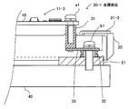
次に本技術の半導体装置の一例として、上記のIPMモジュール2に対して、本技術の半導体装置を適用した際の構成について詳しく説明する。図6は本発明の実施の形態に係る半導体装置の平面図であり、図7は、図6をB方向から見たときの半導体装置の要部を示す部分断面図である。
半導体装置1aは、回路基板10および外囲ケース20を備える。また、外囲ケース20の底面部には放熱ベース板21が位置しており、放熱ベース板21の下面側には、放熱ベース板21を冷却するための冷却フィン40(水冷式、空冷式いずれでもよい)が備えられている。
なお、放熱ベース板21の上面には、回路パターンまたは導電材料が敷設されている絶縁基板22が搭載され、絶縁基板22上には、IGBT23等の半導体素子が実装されている(IGBT等の半導体素子の実装部分については、上述の図4と基本構成は同じであるので説明は省略する)。
樹脂製の外囲ケース20には、回路基板10を取り付けるための金属支柱31が設けられている。回路基板10は、四隅がねじa1~a4(第1のねじに該当)によって金属支柱31に締結されることにより、外囲ケース20の上面に取り付けられている(図7では、金属支柱31に対してねじa1、a2が締結している状態を示している)。
また、回路基板10の表面には、IC、LSI、トランジスタ、抵抗およびコンデンサなどの各回路素子から構成される制御回路11-1~11-6が実装されている。
さらに、回路基板10の表面には、外部接続用のケーブルが挿入されるコネクタ12と、制御端子12-1~12-8が実装されている。
さらに、回路基板10の表面には、外部接続用のケーブルが挿入されるコネクタ12と、制御端子12-1~12-8が実装されている。
制御端子12-1~12-8は、外囲ケース20に内装されているIGBT23のゲート線と、制御回路11-1~11-6とを接続し、制御回路11-1~11-6から送信される制御信号により、IGBT23のスイッチング制御を行う中継端子となっている。
一方、外囲ケース20の額縁部分の一辺には、主端子(U)21-1、主端子(V)21-2および主端子(W)21-3が設けられ、額縁部分の他の一辺には、電源端子(P)22-1および電源端子(N)22-2が設けられている。
主端子(U)21-1、主端子(V)21-2および主端子(W)21-3は、IGBT23のスイッチング制御により、外部のモータを駆動するための端子である。電源端子(P)22-1および電源端子(N)22-2は、外部から電源が供給される端子である。
また、外囲ケース20の額縁四隅には、開口部25-1~25-4が設けられており、開口部25-1~25-4にねじb1~b4(第2のねじに該当)がそれぞれ挿入して締結することにより、外囲ケース20と冷却フィン40とが締結固定されている(図7では、開口部25-1に設けられているリング部32の締結部分のみ示している)。
次に金属部品30について説明する。金属部品30は、図6では、外囲ケース20の額縁四隅のうち、右上の開口部25-1の一箇所に設けられている。なお、これは一例であって、他の開口部25-2~25-4のいずれかに金属部品30を設けてもよいし、一箇所に限らず、複数箇所に金属部品30を設けてもよい。
図7において、金属部品30は、金属支柱31、リング部32および金属バスバー33を備えている。金属支柱31は、外囲ケース20に回路基板10をねじa1で締結固定して取り付けるためのねじ座となり、金属支柱31にねじa1が挿入されて、外囲ケース20に回路基板10が締結固定されている。また、金属支柱31は、外囲ケース20に回路基板10が取り付けられたときには、回路基板10の裏面のGNDパターンに接続される。
リング部32は、外囲ケース20内に含まれている放熱ベース板21と、外囲ケース20とを接続している。また、リング部32は、外囲ケース20に冷却フィン40をねじb1で締結固定して取り付けるためのねじ座となり、リング部32にねじb1が挿入されて、外囲ケース20に冷却フィン40が締結固定されている。
さらに、リング部32は、外囲ケース20の外部に突出したねじb1を通じて接地している。金属バスバー33は、金属支柱31とリング部32とを接続している。
ここで、外囲ケース20の外部に突出したねじb1は、外囲ケース20と冷却フィン40とを締結固定しているので、ねじb1の外囲ケース20からの突出部分は、冷却フィン40の金属面(シャーシ)に接続している。
ここで、外囲ケース20の外部に突出したねじb1は、外囲ケース20と冷却フィン40とを締結固定しているので、ねじb1の外囲ケース20からの突出部分は、冷却フィン40の金属面(シャーシ)に接続している。
そして、回路基板10のGNDパターンは、金属支柱31に接続し、リング部32は、ねじb1を介して冷却フィン40の金属面に接続し、さらに、金属バスバー33は、金属支柱31とリング部32とを接続している。
したがって、回路基板10のGNDパターンは、金属支柱31、金属バスバー33およびリング部32を介して、冷却フィン40の金属面に電気的に接続していることになる。冷却フィン40の金属面は、基準大地面に接地されているので、回路基板10のGNDパターンは、冷却フィン40の金属面を通じて、基準大地面に接地されることになる。
このような半導体装置1aの構成により、回路基板10上で発生したノイズ、または回路基板10に侵入したノイズを、効率よく基準大地面へ放出することができる。このため、回路構成の見直しや後付け部品増加を不要として、耐ノイズ性能の向上を図ることが可能になる。
なお、放熱ベース板21と冷却フィン40との間には、冷却効果を高めるため、例えば、シリコンコンパウンドなどのような絶縁物が挿入される場合がある。
この場合、放熱ベース板21と冷却フィン40との互いの接触面は、電気的に絶縁することになる。しかし、本技術では、冷却フィン40の金属内にねじb1が挿入して、放熱ベース板21を挟んで、外囲ケース20と冷却フィン40とが固定設置される構造となっている。したがって、金属部品30は、ねじb1を介して電気的に接続しており、シリコンコンパウンド等で絶縁されてしまうことはない。
この場合、放熱ベース板21と冷却フィン40との互いの接触面は、電気的に絶縁することになる。しかし、本技術では、冷却フィン40の金属内にねじb1が挿入して、放熱ベース板21を挟んで、外囲ケース20と冷却フィン40とが固定設置される構造となっている。したがって、金属部品30は、ねじb1を介して電気的に接続しており、シリコンコンパウンド等で絶縁されてしまうことはない。
このため、半導体装置1aでは、放熱ベース板21と冷却フィン40との間に、シリコンコンパウンドなどのような絶縁物を挿入しても何ら問題はない。したがって、半導体装置1aにおいても、シリコンコンパウンドなどのような絶縁物を挿入して、放熱ベース板21と冷却フィン40とをより密着させて、熱伝導性を高めて冷却効果を上げることが可能である。
なお、上記では、外部機器4を冷却フィン40としたが、外部機器4としては、その他装置の筐体としてもよい。この場合、外囲ケース20の外部に突出したねじb1によって、外囲ケース20と筐体とが締結固定することにより、回路基板10のGNDパターンが、金属部品30を介して、筐体の金属面に電気的に接続することになり、上記と同様の効果を得ることができる。
次に金属部品30を構成する部品の組み合わせパターンについて説明する。図8は金属部品の構成を示す図である。金属部品30-1は、金属支柱31、リング部32および金属バスバー33の3つの部品を備える。
金属バスバー33の一端は、金属支柱31の先端に設けられている突起部と固定されている。また、金属バスバー33の他端は、ねじb1でリング部32に締結固定されている。
なお、上記では、金属バスバー33の一端は、金属支柱31の先端に設けられている突起部と固定されるとしたが、他の連結方法にしてもよい。
例えば、金属支柱31の凹部と、金属バスバー33を嵌め合わせたり、または金属バスバー33の孔径を広げて、金属支柱31の胴部に嵌め合わせるようにすることも可能である。さらに、ねじa1を金属支柱31の底面から貫通させて、貫通したねじa1の部分で、金属バスバー33の一端を金属支柱31に固定してもよい。
例えば、金属支柱31の凹部と、金属バスバー33を嵌め合わせたり、または金属バスバー33の孔径を広げて、金属支柱31の胴部に嵌め合わせるようにすることも可能である。さらに、ねじa1を金属支柱31の底面から貫通させて、貫通したねじa1の部分で、金属バスバー33の一端を金属支柱31に固定してもよい。
図9~図11は金属部品の他の構成を示す図である。図9に示す金属部品30-2は、金属支柱31、リング部32および金属バスバー33が一体成型した1つの部品となっている。このように、各部品が一体成型されている構成であってもよい。
また、図10に示す金属部品30-3は、金属支柱31と金属バスバー33とが一体成型した部品3aと、リング部32とを備える。この場合、部品3aの金属バスバー33の一端がねじb1でリング部32に締結固定されている。
さらに、図11に示す金属部品30-4は、リング部32と金属バスバー33とが一体成型した部品3bと、金属支柱31とを備える。この場合、部品3bの金属バスバー33の一端がねじa1で金属支柱31に締結固定されている。
このように、金属支柱31と金属バスバー33とが一体成型した部品、またはリング部32と金属バスバー33とが一体成型した部品のいずれかで金属部品30を構成してもよい。なお、金属部品30は、例えばインサート成形等の一体成形により、外囲ケース20に固定されている。
次に半導体装置製造方法のフローについて説明する。図12は本発明の実施の形態に係る半導体装置製造方法のフローチャートを示す図である。
〔S1〕半導体素子が内装されている外囲ケースに設けられた金属支柱に、制御回路が実装されている回路基板を第1のねじで締結固定した際に、回路基板のGNDパターンを金属支柱に接続させる。
〔S1〕半導体素子が内装されている外囲ケースに設けられた金属支柱に、制御回路が実装されている回路基板を第1のねじで締結固定した際に、回路基板のGNDパターンを金属支柱に接続させる。
〔S2〕外囲ケースに設けられたリング部に、外部機器を第2のねじで締結固定した際に、外囲ケースから外部に突出した第2のねじの突出部分を接地させる。
〔S3〕金属支柱とリング部とを金属バスバーで接続する。
〔S3〕金属支柱とリング部とを金属バスバーで接続する。
以上説明したように、半導体装置1は、外囲ケースへ回路基板を取り付け、回路基板の接地パターンと接続する第1の取付部と、外囲ケースへ外部機器を取り付け、接地する第2の取付部と、第1、第2の取付部を互いに接続するバスバーとを含む金属部品を備える構成とした。
これにより、回路構成の見直しや後付け部品増加を不要として、耐ノイズ性能の向上を図ることが可能になる。
また、回路基板のGNDパターンを、金属部品を介して、基準GND(基準大地面)へ最短距離で接続するので、配線インダクタを大幅に低減して、耐ノイズ性能を向上させることが可能になる。さらに、高周波数帯までのノイズ信号耐用試験に対応することも可能になる。
また、回路基板のGNDパターンを、金属部品を介して、基準GND(基準大地面)へ最短距離で接続するので、配線インダクタを大幅に低減して、耐ノイズ性能を向上させることが可能になる。さらに、高周波数帯までのノイズ信号耐用試験に対応することも可能になる。
さらにまた、半導体装置製造方法は、外囲ケースに設けられた金属支柱に回路基板をねじで締結固定した際に、回路基板の接地パターンを金属支柱に接続させる。また、外囲ケースに設けられたリング部に外部機器をねじで締結固定した際に、ねじを外部に突出させて接地させる。そして、金属支柱とリング部とを金属バスバーで接続して半導体装置を製造することとした。
これにより、回路構成の見直しや後付け部品増加を不要として、耐ノイズ性能の向上を図ることが可能になる。また、回路基板のGNDパターンを、金属部品を介して、基準GND(基準大地面)へ最短距離で接続するので、配線インダクタを大幅に低減して、耐ノイズ性能を向上させることが可能になる。さらに、高周波数帯までのノイズ信号耐用試験に対応することも可能になる。
以上、実施の形態を例示したが、実施の形態で示した各部の構成は同様の機能を有する他のものに置換することができる。また、他の任意の構成物や工程が付加されてもよい。
上記については単に本発明の原理を示すものである。さらに、多数の変形、変更が当業者にとって可能であり、本発明は上記に示し、説明した正確な構成および応用例に限定されるものではなく、対応するすべての変形例および均等物は、添付の請求項およびその均等物による本発明の範囲とみなされる。
上記については単に本発明の原理を示すものである。さらに、多数の変形、変更が当業者にとって可能であり、本発明は上記に示し、説明した正確な構成および応用例に限定されるものではなく、対応するすべての変形例および均等物は、添付の請求項およびその均等物による本発明の範囲とみなされる。
1 半導体装置
10 回路基板
11 制御回路
20 外囲ケース
23 半導体素子
30 金属部品
31a 第1の取付部
32a 第2の取付部
33a バスバー
4 外部機器
10 回路基板
11 制御回路
20 外囲ケース
23 半導体素子
30 金属部品
31a 第1の取付部
32a 第2の取付部
33a バスバー
4 外部機器
Claims (13)
- 半導体素子が内装されている外囲ケースと、
制御回路が実装されている回路基板と、
前記外囲ケースに前記回路基板を取り付け、取り付け時に前記回路基板の接地パターンと接続する第1の取付部と、前記外囲ケースに外部機器を取り付け、取り付け時に接地する第2の取付部とを有し、前記第1の取付部と前記第2の取付部とをバスバーで接続する金属部品と、
を有することを特徴とする半導体装置。 - 前記金属部品は、
前記外囲ケースに前記回路基板を第1のねじで締結固定して取り付けるためのねじ座となり、前記回路基板の接地パターンと接続する、前記第1の取付部である金属支柱と、
前記外囲ケースに前記外部機器を第2のねじで締結固定して取り付けるためのねじ座となり、前記外囲ケースの外部に突出した前記第2のねじを通じて接地する、前記第2の取付部である金属製のリング部と、
前記金属支柱と前記リング部とを接続する、前記バスバーである金属バスバーと、
を備えることを特徴とする請求の範囲第1項記載の半導体装置。 - 前記外囲ケースの外部に突出した前記第2のねじによって、前記外囲ケースと前記外部機器である冷却フィンとが締結固定することにより、前記回路基板の接地パターンが、前記金属部品を介して、前記冷却フィンの金属面に電気的に接続することを特徴とする請求の範囲第2項記載の半導体装置。
- 前記外囲ケースの外部に突出した前記第2のねじによって、前記外囲ケースと前記外部機器である筐体とが締結固定することにより、前記回路基板の接地パターンが、前記金属部品を介して、前記筐体の金属面に電気的に接続することを特徴とする請求の範囲第2項記載の半導体装置。
- 前記金属支柱、前記リング部および前記金属バスバーは、個別の部品であり、前記金属バスバーの一端は、前記金属支柱の先端に設けられている突起部と固定され、前記金属バスバーの他端は、前記第2のねじで前記リング部に締結固定されていることを特徴とする請求の範囲第2項記載の半導体装置。
- 前記金属支柱、前記リング部および前記金属バスバーは、一体成型した1つの部品であることを特徴とする請求の範囲第2項記載の半導体装置。
- 前記金属支柱、前記リング部および前記金属バスバーは、前記金属支柱と前記金属バスバーとが一体成型した部品、または前記金属バスバーと前記リング部とが一体成型した部品のいずれかであることを特徴とする請求の範囲第2項記載の半導体装置。
- 半導体装置製造方法において、
半導体素子が内装されている外囲ケースに設けられている金属支柱に、制御回路が実装されている回路基板を第1のねじで締結固定した際に、前記回路基板の接地パターンを前記金属支柱に接続させ、
前記外囲ケースに設けられているリング部に、外部機器を第2のねじで締結固定した際に、前記外囲ケースから外部に突出した前記第2のねじの突出部分を接地させ、
前記金属支柱と前記リング部とを金属バスバーで接続して、半導体装置を製造する半導体装置製造方法。 - 前記外囲ケースの外部に突出した前記第2のねじによって、前記外囲ケースと前記外部機器である冷却フィンとを締結固定して、前記回路基板の接地パターンを、前記冷却フィンの金属面に電気的に接続させることを特徴とする請求の範囲第8項記載の半導体装置製造方法。
- 前記外囲ケースの外部に突出した前記第2のねじによって、前記外囲ケースと前記外部機器である筐体とを締結固定して、前記回路基板の接地パターンを、前記筐体の金属面に電気的に接続させることを特徴とする請求の範囲第8項記載の半導体装置製造方法。
- 前記金属支柱、前記リング部および前記金属バスバーは、個別の部品であり、前記金属バスバーの一端は、前記第1のねじで前記金属支柱に締結固定させ、前記金属バスバーの他端は、前記第2のねじで前記リング部に締結固定させることを特徴とする請求の範囲第8項記載の半導体装置製造方法。
- 前記金属支柱、前記リング部および前記金属バスバーは、一体成型した1つの部品であることを特徴とする請求の範囲第8項記載の半導体装置製造方法。
- 前記金属支柱、前記リング部および前記金属バスバーは、前記金属支柱と前記金属バスバーとが一体成型した部品、または前記金属バスバーと前記リング部とが一体成型した部品のいずれかであることを特徴とする請求の範囲第8項記載の半導体装置製造方法。
Priority Applications (3)
| Application Number | Priority Date | Filing Date | Title |
|---|---|---|---|
| CN201280055736.8A CN103930991B (zh) | 2011-12-08 | 2012-10-12 | 半导体器件及半导体器件制造方法 |
| EP12855732.9A EP2790216B1 (en) | 2011-12-08 | 2012-10-12 | Semiconductor device and semiconductor device manufacturing method |
| US14/276,665 US9576913B2 (en) | 2011-12-08 | 2014-05-13 | Semiconductor device and manufacturing method of semiconductor device |
Applications Claiming Priority (2)
| Application Number | Priority Date | Filing Date | Title |
|---|---|---|---|
| JP2011-269190 | 2011-12-08 | ||
| JP2011269190 | 2011-12-08 |
Related Child Applications (1)
| Application Number | Title | Priority Date | Filing Date |
|---|---|---|---|
| US14/276,665 Continuation US9576913B2 (en) | 2011-12-08 | 2014-05-13 | Semiconductor device and manufacturing method of semiconductor device |
Publications (1)
| Publication Number | Publication Date |
|---|---|
| WO2013084589A1 true WO2013084589A1 (ja) | 2013-06-13 |
Family
ID=48573972
Family Applications (1)
| Application Number | Title | Priority Date | Filing Date |
|---|---|---|---|
| PCT/JP2012/076452 Ceased WO2013084589A1 (ja) | 2011-12-08 | 2012-10-12 | 半導体装置および半導体装置製造方法 |
Country Status (5)
| Country | Link |
|---|---|
| US (1) | US9576913B2 (ja) |
| EP (1) | EP2790216B1 (ja) |
| JP (1) | JPWO2013084589A1 (ja) |
| CN (1) | CN103930991B (ja) |
| WO (1) | WO2013084589A1 (ja) |
Cited By (4)
| Publication number | Priority date | Publication date | Assignee | Title |
|---|---|---|---|---|
| JP2017037951A (ja) * | 2015-08-10 | 2017-02-16 | 日産自動車株式会社 | 電力変換装置 |
| EP3057217A4 (en) * | 2013-10-07 | 2017-07-12 | Hitachi Automotive Systems, Ltd. | Power conversion device |
| JP2018139278A (ja) * | 2017-02-24 | 2018-09-06 | 三菱電機株式会社 | 半導体装置、半導体装置の製造方法 |
| JP2023541621A (ja) * | 2020-09-15 | 2023-10-03 | 華為技術有限公司 | パワーモジュール及びその製造方法、コンバータ、並びに電子機器 |
Families Citing this family (22)
| Publication number | Priority date | Publication date | Assignee | Title |
|---|---|---|---|---|
| JP5991440B2 (ja) * | 2013-09-10 | 2016-09-14 | 三菱電機株式会社 | 半導体装置、半導体モジュール |
| JP2015056614A (ja) * | 2013-09-13 | 2015-03-23 | 株式会社東芝 | 半導体装置部品および半導体装置 |
| JP6323557B2 (ja) * | 2014-07-17 | 2018-05-16 | 富士電機株式会社 | 半導体装置 |
| CN105870073B (zh) * | 2015-01-22 | 2019-02-15 | 台达电子工业股份有限公司 | 功率模块的封装结构 |
| TWI557857B (zh) * | 2015-01-22 | 2016-11-11 | 台達電子工業股份有限公司 | 功率模組之封裝結構 |
| JP6119787B2 (ja) * | 2015-03-31 | 2017-04-26 | トヨタ自動車株式会社 | ケース体に対する回路基板の姿勢維持構造 |
| EP3196932A1 (en) * | 2016-01-21 | 2017-07-26 | ABB Technology Oy | Cooled electrical assembly |
| US10347549B2 (en) * | 2016-04-30 | 2019-07-09 | Littelfuse, Inc. | Power semiconductor device module having mechanical corner press-fit anchors |
| US10062621B2 (en) * | 2016-04-30 | 2018-08-28 | Ixys, Llc | Power semiconductor device module having mechanical corner press-fit anchors |
| DE112016007133B4 (de) * | 2016-08-10 | 2021-08-12 | Mitsubishi Electric Corporation | Halbleitervorrichtung |
| JP6750416B2 (ja) * | 2016-09-14 | 2020-09-02 | 富士電機株式会社 | 半導体モジュールおよび半導体モジュールの製造方法 |
| JP6818877B2 (ja) * | 2017-04-20 | 2021-01-20 | 三菱電機株式会社 | 電力変換装置 |
| WO2018230030A1 (ja) * | 2017-06-14 | 2018-12-20 | 三菱電機株式会社 | 電流検出装置及び電力変換装置 |
| DE102018118181A1 (de) | 2018-07-27 | 2020-01-30 | Ebm-Papst Mulfingen Gmbh & Co. Kg | Steuerungselektronik in modularer Bauweise |
| DE102019109461A1 (de) * | 2019-04-10 | 2020-10-15 | Schaeffler Technologies AG & Co. KG | Leistungsmodul mit zwischenkreiskondensator |
| JP2021019487A (ja) * | 2019-07-24 | 2021-02-15 | 株式会社デンソー | 半導体モジュール構造 |
| DE102019133678B4 (de) * | 2019-12-10 | 2024-04-04 | Audi Ag | Anordnung für elektronische Bauteile |
| EP3852138B1 (en) | 2020-01-20 | 2023-11-08 | Infineon Technologies Austria AG | An electronic module comprising a semiconductor package connected to a fluid heatsink |
| US12495511B2 (en) * | 2021-03-10 | 2025-12-09 | Hitachi Astemo, Ltd. | Electronic control device |
| JP7595757B2 (ja) * | 2021-05-11 | 2024-12-06 | 三菱電機株式会社 | 電力変換装置 |
| JP7183373B1 (ja) * | 2021-11-15 | 2022-12-05 | 三菱電機株式会社 | 電力変換装置 |
| DE102024202691A1 (de) * | 2024-03-21 | 2025-09-25 | Zf Friedrichshafen Ag | Verbindungssystem zwischen mindestens einer Leiterplatte und einem Gehäuse |
Citations (6)
| Publication number | Priority date | Publication date | Assignee | Title |
|---|---|---|---|---|
| JPH08293578A (ja) * | 1995-04-21 | 1996-11-05 | Toshiba Corp | 半導体装置 |
| JP2001211663A (ja) * | 2000-01-28 | 2001-08-03 | Sanden Corp | モータ駆動用インバータ装置 |
| JP3196540B2 (ja) | 1994-12-09 | 2001-08-06 | 富士電機株式会社 | 半導体装置 |
| JP2005085840A (ja) * | 2003-09-05 | 2005-03-31 | Mitsubishi Electric Corp | 電力用半導体装置 |
| JP3750427B2 (ja) | 1999-07-23 | 2006-03-01 | 富士電機デバイステクノロジー株式会社 | 半導体装置 |
| WO2010150471A1 (en) * | 2009-06-25 | 2010-12-29 | Fuji Electric Systems Co., Ltd. | Semiconductor device |
Family Cites Families (12)
| Publication number | Priority date | Publication date | Assignee | Title |
|---|---|---|---|---|
| US4574470A (en) * | 1984-03-19 | 1986-03-11 | Trilogy Computer Development Partners, Ltd. | Semiconductor chip mounting system |
| JP4218193B2 (ja) * | 2000-08-24 | 2009-02-04 | 三菱電機株式会社 | パワーモジュール |
| DE10254910B4 (de) * | 2001-11-26 | 2008-12-24 | AutoNetworks Technologies, Ltd., Nagoya | Schaltkreisbildende Einheit und Verfahren zu deren Herstellung |
| JP3813098B2 (ja) * | 2002-02-14 | 2006-08-23 | 三菱電機株式会社 | 電力用半導体モジュール |
| JP4022440B2 (ja) * | 2002-07-01 | 2007-12-19 | 株式会社オートネットワーク技術研究所 | 回路ユニット |
| KR100488518B1 (ko) * | 2002-11-14 | 2005-05-11 | 삼성전자주식회사 | 반도체 장치의 방열 시스템 |
| JP4404726B2 (ja) * | 2004-08-31 | 2010-01-27 | 三菱電機株式会社 | 車載用電力変換装置 |
| JP4615289B2 (ja) * | 2004-11-12 | 2011-01-19 | 三菱電機株式会社 | 半導体装置 |
| DE102006018161A1 (de) * | 2006-04-19 | 2007-10-25 | Patent-Treuhand-Gesellschaft für elektrische Glühlampen mbH | Elektronisches Bauelementmodul |
| DE102009017621B3 (de) * | 2009-04-16 | 2010-08-19 | Semikron Elektronik Gmbh & Co. Kg | Vorrichtung zur Verringerung der Störabstrahlung in einem leistungselektronischen System |
| JP5219290B2 (ja) * | 2009-06-02 | 2013-06-26 | 株式会社ケーヒン | グラウンド端子を有する電子装置 |
| JP2011216619A (ja) * | 2010-03-31 | 2011-10-27 | Nippon Steel Chem Co Ltd | 積層構造体及びその製造方法 |
-
2012
- 2012-10-12 CN CN201280055736.8A patent/CN103930991B/zh active Active
- 2012-10-12 EP EP12855732.9A patent/EP2790216B1/en active Active
- 2012-10-12 WO PCT/JP2012/076452 patent/WO2013084589A1/ja not_active Ceased
- 2012-10-12 JP JP2013548139A patent/JPWO2013084589A1/ja active Pending
-
2014
- 2014-05-13 US US14/276,665 patent/US9576913B2/en active Active
Patent Citations (6)
| Publication number | Priority date | Publication date | Assignee | Title |
|---|---|---|---|---|
| JP3196540B2 (ja) | 1994-12-09 | 2001-08-06 | 富士電機株式会社 | 半導体装置 |
| JPH08293578A (ja) * | 1995-04-21 | 1996-11-05 | Toshiba Corp | 半導体装置 |
| JP3750427B2 (ja) | 1999-07-23 | 2006-03-01 | 富士電機デバイステクノロジー株式会社 | 半導体装置 |
| JP2001211663A (ja) * | 2000-01-28 | 2001-08-03 | Sanden Corp | モータ駆動用インバータ装置 |
| JP2005085840A (ja) * | 2003-09-05 | 2005-03-31 | Mitsubishi Electric Corp | 電力用半導体装置 |
| WO2010150471A1 (en) * | 2009-06-25 | 2010-12-29 | Fuji Electric Systems Co., Ltd. | Semiconductor device |
Non-Patent Citations (1)
| Title |
|---|
| See also references of EP2790216A4 |
Cited By (9)
| Publication number | Priority date | Publication date | Assignee | Title |
|---|---|---|---|---|
| EP3057217A4 (en) * | 2013-10-07 | 2017-07-12 | Hitachi Automotive Systems, Ltd. | Power conversion device |
| US9814154B2 (en) | 2013-10-07 | 2017-11-07 | Hitachi Automotive Systems, Ltd. | Power converter |
| JP2017037951A (ja) * | 2015-08-10 | 2017-02-16 | 日産自動車株式会社 | 電力変換装置 |
| JP2018139278A (ja) * | 2017-02-24 | 2018-09-06 | 三菱電機株式会社 | 半導体装置、半導体装置の製造方法 |
| US10340217B2 (en) | 2017-02-24 | 2019-07-02 | Mitsubishi Electric Corporation | Semiconductor device including a cylindrical electrode inserted into a looped portion of an electrode |
| US10651121B2 (en) | 2017-02-24 | 2020-05-12 | Mitsubishi Electric Corporation | Semiconductor device manufacturing method including forming a wide portion spreading over a looped portion |
| DE102017223094B4 (de) | 2017-02-24 | 2022-04-28 | Mitsubishi Electric Corporation | Halbleitervorrichtung und Herstellungsverfahren für eine Halbleitervorrichtung |
| JP2023541621A (ja) * | 2020-09-15 | 2023-10-03 | 華為技術有限公司 | パワーモジュール及びその製造方法、コンバータ、並びに電子機器 |
| JP7691208B2 (ja) | 2020-09-15 | 2025-06-11 | 華為技術有限公司 | パワーモジュール及びその製造方法、コンバータ、並びに電子機器 |
Also Published As
| Publication number | Publication date |
|---|---|
| CN103930991A (zh) | 2014-07-16 |
| US9576913B2 (en) | 2017-02-21 |
| EP2790216A4 (en) | 2015-10-07 |
| CN103930991B (zh) | 2018-05-22 |
| EP2790216A1 (en) | 2014-10-15 |
| JPWO2013084589A1 (ja) | 2015-04-27 |
| EP2790216B1 (en) | 2020-01-22 |
| US20140246768A1 (en) | 2014-09-04 |
Similar Documents
| Publication | Publication Date | Title |
|---|---|---|
| WO2013084589A1 (ja) | 半導体装置および半導体装置製造方法 | |
| JP3501685B2 (ja) | 電力変換装置 | |
| JP3516789B2 (ja) | 半導体パワーモジュール | |
| US6313991B1 (en) | Power electronics system with fully-integrated cooling | |
| US9978672B1 (en) | Transistor package with terminals coupled via chip carrier | |
| US10163752B2 (en) | Semiconductor device | |
| CN104604354A (zh) | 车载用功率转换装置 | |
| JP2007227957A (ja) | 半導体装置モジュール | |
| JPWO2016031462A1 (ja) | パワー半導体モジュール | |
| CN216930700U (zh) | 功率模块 | |
| JP2001186778A (ja) | 電力変換装置 | |
| JP5968542B2 (ja) | パワーモジュール | |
| CN111385985B (zh) | 电动车集成控制器 | |
| CN117558719A (zh) | 一种功率变换器、封装结构以及散热结构 | |
| JP6745386B1 (ja) | 電力変換装置 | |
| US20150001702A1 (en) | Semiconductor module and semiconductor device | |
| CN110364499B (zh) | 多封装顶侧冷却 | |
| CN106061143A (zh) | 电子控制单元 | |
| US8890313B2 (en) | Through-hole electronic device with double heat-sink | |
| CN113853737B (zh) | 电力转换装置及电力转换装置的制造方法 | |
| JP4055643B2 (ja) | インバータ装置 | |
| US9202766B2 (en) | Package for power device and method of making the same | |
| US8816515B2 (en) | Semiconductor module having sliding case and manufacturing method thereof | |
| JP2010177453A (ja) | 半導体装置 | |
| JP3482913B2 (ja) | 半導体モジュール |
Legal Events
| Date | Code | Title | Description |
|---|---|---|---|
| 121 | Ep: the epo has been informed by wipo that ep was designated in this application |
Ref document number: 12855732 Country of ref document: EP Kind code of ref document: A1 |
|
| ENP | Entry into the national phase |
Ref document number: 2013548139 Country of ref document: JP Kind code of ref document: A |
|
| WWE | Wipo information: entry into national phase |
Ref document number: 2012855732 Country of ref document: EP |
|
| NENP | Non-entry into the national phase |
Ref country code: DE |