WO2013084778A1 - プリディストータ、プリディストータ制御方法 - Google Patents
プリディストータ、プリディストータ制御方法 Download PDFInfo
- Publication number
- WO2013084778A1 WO2013084778A1 PCT/JP2012/080864 JP2012080864W WO2013084778A1 WO 2013084778 A1 WO2013084778 A1 WO 2013084778A1 JP 2012080864 W JP2012080864 W JP 2012080864W WO 2013084778 A1 WO2013084778 A1 WO 2013084778A1
- Authority
- WO
- WIPO (PCT)
- Prior art keywords
- signal
- distortion
- carrier
- sub
- band
- Prior art date
- Legal status (The legal status is an assumption and is not a legal conclusion. Google has not performed a legal analysis and makes no representation as to the accuracy of the status listed.)
- Ceased
Links
Images









Classifications
-
- H—ELECTRICITY
- H03—ELECTRONIC CIRCUITRY
- H03F—AMPLIFIERS
- H03F1/00—Details of amplifiers with only discharge tubes, only semiconductor devices or only unspecified devices as amplifying elements
- H03F1/32—Modifications of amplifiers to reduce non-linear distortion
- H03F1/3241—Modifications of amplifiers to reduce non-linear distortion using predistortion circuits
- H03F1/3247—Modifications of amplifiers to reduce non-linear distortion using predistortion circuits using feedback acting on predistortion circuits
-
- H—ELECTRICITY
- H03—ELECTRONIC CIRCUITRY
- H03F—AMPLIFIERS
- H03F1/00—Details of amplifiers with only discharge tubes, only semiconductor devices or only unspecified devices as amplifying elements
- H03F1/32—Modifications of amplifiers to reduce non-linear distortion
- H03F1/3241—Modifications of amplifiers to reduce non-linear distortion using predistortion circuits
-
- H—ELECTRICITY
- H03—ELECTRONIC CIRCUITRY
- H03F—AMPLIFIERS
- H03F3/00—Amplifiers with only discharge tubes or only semiconductor devices as amplifying elements
- H03F3/189—High-frequency amplifiers, e.g. radio frequency amplifiers
- H03F3/19—High-frequency amplifiers, e.g. radio frequency amplifiers with semiconductor devices only
-
- H—ELECTRICITY
- H03—ELECTRONIC CIRCUITRY
- H03F—AMPLIFIERS
- H03F3/00—Amplifiers with only discharge tubes or only semiconductor devices as amplifying elements
- H03F3/20—Power amplifiers, e.g. Class B amplifiers, Class C amplifiers
- H03F3/24—Power amplifiers, e.g. Class B amplifiers, Class C amplifiers of transmitter output stages
- H03F3/245—Power amplifiers, e.g. Class B amplifiers, Class C amplifiers of transmitter output stages with semiconductor devices only
-
- H—ELECTRICITY
- H04—ELECTRIC COMMUNICATION TECHNIQUE
- H04B—TRANSMISSION
- H04B1/00—Details of transmission systems, not covered by a single one of groups H04B3/00 - H04B13/00; Details of transmission systems not characterised by the medium used for transmission
- H04B1/02—Transmitters
- H04B1/04—Circuits
- H04B1/0475—Circuits with means for limiting noise, interference or distortion
-
- H—ELECTRICITY
- H04—ELECTRIC COMMUNICATION TECHNIQUE
- H04L—TRANSMISSION OF DIGITAL INFORMATION, e.g. TELEGRAPHIC COMMUNICATION
- H04L27/00—Modulated-carrier systems
- H04L27/32—Carrier systems characterised by combinations of two or more of the types covered by groups H04L27/02, H04L27/10, H04L27/18 or H04L27/26
- H04L27/34—Amplitude- and phase-modulated carrier systems, e.g. quadrature-amplitude modulated carrier systems
- H04L27/36—Modulator circuits; Transmitter circuits
- H04L27/366—Arrangements for compensating undesirable properties of the transmission path between the modulator and the demodulator
- H04L27/367—Arrangements for compensating undesirable properties of the transmission path between the modulator and the demodulator using predistortion
- H04L27/368—Arrangements for compensating undesirable properties of the transmission path between the modulator and the demodulator using predistortion adaptive predistortion
-
- H—ELECTRICITY
- H04—ELECTRIC COMMUNICATION TECHNIQUE
- H04L—TRANSMISSION OF DIGITAL INFORMATION, e.g. TELEGRAPHIC COMMUNICATION
- H04L27/00—Modulated-carrier systems
- H04L27/32—Carrier systems characterised by combinations of two or more of the types covered by groups H04L27/02, H04L27/10, H04L27/18 or H04L27/26
- H04L27/34—Amplitude- and phase-modulated carrier systems, e.g. quadrature-amplitude modulated carrier systems
- H04L27/38—Demodulator circuits; Receiver circuits
- H04L27/3818—Demodulator circuits; Receiver circuits using coherent demodulation, i.e. using one or more nominally phase synchronous carriers
-
- H—ELECTRICITY
- H03—ELECTRONIC CIRCUITRY
- H03F—AMPLIFIERS
- H03F2200/00—Indexing scheme relating to amplifiers
- H03F2200/336—A I/Q, i.e. phase quadrature, modulator or demodulator being used in an amplifying circuit
-
- H—ELECTRICITY
- H04—ELECTRIC COMMUNICATION TECHNIQUE
- H04B—TRANSMISSION
- H04B1/00—Details of transmission systems, not covered by a single one of groups H04B3/00 - H04B13/00; Details of transmission systems not characterised by the medium used for transmission
- H04B1/02—Transmitters
- H04B1/04—Circuits
- H04B2001/0408—Circuits with power amplifiers
- H04B2001/0425—Circuits with power amplifiers with linearisation using predistortion
-
- H—ELECTRICITY
- H04—ELECTRIC COMMUNICATION TECHNIQUE
- H04L—TRANSMISSION OF DIGITAL INFORMATION, e.g. TELEGRAPHIC COMMUNICATION
- H04L5/00—Arrangements affording multiple use of the transmission path
- H04L5/0001—Arrangements for dividing the transmission path
- H04L5/0003—Two-dimensional division
- H04L5/0005—Time-frequency
- H04L5/0007—Time-frequency the frequencies being orthogonal, e.g. OFDM(A) or DMT
- H04L5/001—Time-frequency the frequencies being orthogonal, e.g. OFDM(A) or DMT the frequencies being arranged in component carriers
Definitions
- the present invention relates to a predistorter that compensates for distortion components generated in a power amplifier and a predistorter control method.
- Non-Patent Document 1 and Non-Patent Document 2 use a model of nonlinear characteristics based on a power series to generate a distortion compensation signal capable of compensating for a distortion component having frequency dependence.
- the output signal y (t) of the predistorter can be expressed as in Equation (1). .
- the second term is a distortion compensation signal
- 2 x (t) represents a third-order distortion component generated by the third-order distortion generator of the predistorter
- a 1 is a linear gain.
- a 3 represents a complex coefficient given to a third-order distortion vector adjuster that adjusts the amplitude and phase of the third-order distortion component
- h 3 (t) represents a frequency that gives a frequency characteristic to the output of the third-order distortion vector adjuster. It represents the impulse response of the characteristic compensator, and * (asterisk) represents convolution.
- the distortion compensation signal is generated by digital signal processing.
- a 3 and h 3 (t) are appropriately adjusted so that the distortion component having frequency dependency generated in the power amplifier is reduced.
- CA carrier aggregation
- carriers frequency bands
- CA carrier aggregation
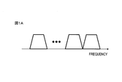
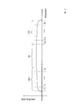
- FIG. 1A a case where a continuous frequency band is used as shown in FIG. 1A
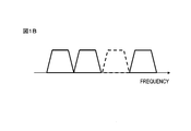
- FIG. 1B a case where a discontinuous frequency band is used as shown in FIG. 1B.
- FIG. 1B shows an example in which the frequency bands are relatively close to each other, there are cases where the frequency bands are widely separated.
- the signal transmitted using the first frequency band is s 1 (t)
- the signal transmitted using the second frequency band is s 2 (t)
- the input signal x (t) of the predistorter is x
- (t) s 1 (t) + s 2 (t)
- the output signal y (t) of the predistorter can be expressed as in equation (2).
- Equation (2) if the third-order distortion component generated by the third-order distortion generator of the predistorter is d C (t), d C (t) can be expressed as Equation (3).
- predistorter in the case of using a plurality of frequency bands, there is a predistorter prepared independently for each frequency band as in, for example, “JP 2006-191673 A (Reference 1)”.
- a predistorter is prepared independently for each frequency band, so that the intermodulation distortion components of s 1 (t) and s 2 (t) cannot be generated by the predistorter. Therefore, even when the predistorter of Reference 1 is used, distortion components generated in the power amplifier remain.
- the conventional predistorter has a problem that the intermodulation distortion components of s 1 (t) and s 2 (t) cannot be sufficiently reduced.
- the present invention has been made in view of such a point, and an object thereof is to provide a predistorter capable of compensating for an intermodulation distortion component generated in a power amplifier even when CA is used.
- the predistorter of the present invention includes a linear transmission path, a plurality of signal generation units, a sub-signal generation unit, a signal distribution unit, a signal synthesis unit, and a control unit.
- the linear transmission path transmits an input signal including a plurality of carriers with a delay.
- the plurality of signal generators For each carrier included in the input signal, the plurality of signal generators generate an individual carrier distortion signal that is a distortion component generated by the carrier, adjust the individual carrier distortion signal, and output an individual carrier distortion compensation signal .
- the sub-signal generating unit generates an intermodulation distortion signal generated between carriers from the input signal and the individual carrier distortion signal, and extracts at least a component in the same frequency band as the carrier from the intermodulation distortion signal.
- a modulation distortion signal is generated, the carrier intermodulation distortion signal is adjusted, and a carrier intermodulation distortion compensation signal is output.
- the signal distribution unit distributes the input signal to the linear transmission path, the signal generation unit, and the sub signal generation unit.
- the signal synthesis unit generates a distortion compensation signal by combining the individual carrier distortion compensation signal and the carrier intermodulation distortion compensation signal, and generates an output signal by combining the input signal delayed by the linear transmission path and the distortion compensation signal. Then, the output signal is output to the amplification device.
- the control unit controls the signal generation unit and the sub signal generation unit using a feedback signal from the amplification device.
- an intermodulation distortion compensation signal corresponding to an intermodulation distortion component between carriers can be independently generated by the sub-signal generation unit, and the phase and amplitude of the signal are independently adjusted. Therefore, even when CA is used, the intermodulation distortion component generated in the power amplifier can be compensated.
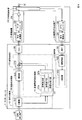
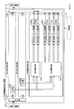
- FIG. 2 is a block diagram illustrating the overall configuration of the predistorter according to the first embodiment.
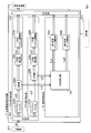
- FIG. 3 is a block diagram illustrating a configuration of a distortion compensation signal generation path according to the first embodiment.
- produces with a power amplifier.
- FIG. 10 is a block diagram illustrating the overall configuration of a predistorter according to a first modification.
- FIG. 6 is a block diagram illustrating a configuration of a distortion compensation signal generation path according to a first modification.
- FIG. Flowchart P14 of the control method in the predistorter of Example 1 Modification 2.
- FIG. 3 is a block diagram illustrating an overall configuration of a predistorter according to a second embodiment.
- FIG. 6 is a block diagram illustrating a configuration of a distortion compensation signal generation path according to the second embodiment.
- Embodiment 2 A block diagram showing an overall configuration of a predistorter according to a first modification.
- Embodiment 2 A block diagram showing a configuration of a distortion compensation signal generation path of a first modification.
- Embodiment 2 The block diagram which shows the whole structure of the predistorter of the modification 2.
- Embodiment 2 A block diagram showing a configuration of a distortion compensation signal generation path of a second modification.
- FIG. 9 is a block diagram illustrating an overall configuration of a predistorter according to a third embodiment.
- FIG. 10 is a block diagram illustrating a configuration of a distortion compensation signal generation path according to the third embodiment.
- FIG. The flowchart P33 of the control method in the predistorter of Example 3.
- FIG. 10 is a block diagram illustrating a configuration of a distortion compensation signal generation path according to a modification of the third embodiment.
- FIG. 9 is a block diagram illustrating the overall configuration of a predistorter according to a fourth embodiment.
- FIG. 1 is a block diagram illustrating a configuration of a distortion compensation signal generation path according to a fourth embodiment.
- FIG. 2 is a block diagram illustrating a configuration of a distortion compensation signal generation path according to a fourth embodiment.
- the signal transmitted using the first frequency band is s 1 (t)
- the signal transmitted using the second frequency band is s 2 (t)
- s 1 (t) can be extracted from x (t) by using a digital filter such as an FIR filter.
- a third-order distortion component d A (t)
- 2 s 1 (t) is generated from the extracted s 1 (t).
- the intermodulation distortion components d CA (t) and d CB (t) that can be expressed by the expressions (A-2) and (A-3) are extracted from the expression (A-1).
- each distortion component generated in the same frequency band is extracted.
- the phase and amplitude of the extracted intermodulation distortion components d A (t), d B (t), d CA (t), and d CB (t) are individually adjusted to obtain a distortion compensation signal.
- FIG. 2 is a block diagram showing the overall configuration of the predistorter 10 and peripheral devices according to this embodiment.
- FIG. 3 is a block diagram showing a configuration of a distortion compensation signal generation path 110 included in the predistorter 10 according to the present embodiment.
- Peripheral devices of this embodiment are an amplification device 20, a feedback signal generation device 30, a signal generation device 40, and an output terminal 50.
- the predistorter 10 of this embodiment includes a distortion compensation signal generation path 110, a control section 140, a linear transmission path 150, a signal distribution section 160, a signal synthesis section 170, a digital / analog converter (hereinafter referred to as DAC) 180, and an analog digital.
- a converter hereinafter referred to as ADC 190 is included.
- the signal generator 40 includes an I-phase signal and a Q-phase signal (hereinafter also referred to as an I / Q signal), and has different N B (hereinafter, N B represents a predetermined integer of 2 or more) frequency bands.
- N B represents a predetermined integer of 2 or more
- An input signal which is a digital signal used simultaneously is output. In the following description, as an example the case where the N B and 2.
- the signal distributor 160 includes a distributor 1610 and a distributor 1620.
- the distributor 1610 distributes the input signal output from the signal generator 40 to the linear transmission path 150 and the distortion compensation signal generation path 110.
- the distribution unit 1620 will be described in the description of the distortion compensation signal generation path 110 described later.
- the linear transmission path 150 includes a delay unit 1510.
- the delay unit 1510 delays the input signal by a delay time generated in the distortion compensation signal generation path 110.
- the signal synthesis unit 170 includes an adder 1710 and a synthesis unit 1720.
- the adder 1710 combines the input signal output from the linear transfer path 150 and the distortion compensation signal output from the distortion compensation signal generation path 110.
- the combining unit 1720 will be described in the description of the distortion compensation signal generation path 110 described later.
- the DAC 180 converts the digital signal output from the signal synthesis unit 170 into an analog signal.
- the amplification device 20 includes a quadrature modulator 210, an up-converter 220, and a power amplifier 230.
- the quadrature modulator 210 performs quadrature modulation on the analog signal output from the DAC 180.
- the up-converter 220 up-converts the signal output from the quadrature modulator 210 to a target frequency.
- the power amplifier 230 amplifies the signal output from the up-converter 220 to a target power.
- the output terminal 50 supplies the signal output from the amplification device 20 to the antenna via a duplexer or the like (not shown).
- the feedback signal generation device 30 includes a directional coupler 310, a down converter 320, and a quadrature demodulator 330.
- the directional coupler 310 takes a part of the signal output from the amplification device 20 into the feedback signal generation device 30.
- the down converter 320 down-converts the signal output from the directional coupler 310 to a predetermined frequency.
- the quadrature demodulator 330 demodulates the signal output from the down converter 320 into an I-phase signal and a Q-phase signal and generates a feedback signal.
- the ADC 190 converts the analog signal output from the feedback signal generator 30 into a digital signal.
- the control unit 140 includes a controller 1410 and a strain observer 1420.
- the distortion observer 1420 measures the distortion component power generated by the power amplifier 230 from the digital signal output from the ADC 190 for each bandwidth designated in advance.
- the controller 1410 refers to the observation result output from the distortion observer 1420 and controls the distortion compensation signal generation path 110 so as to reduce the distortion component generated in the power amplifier 230. Details of the operation of the controller 1410 will be described later.
- the distortion compensation signal generation path 110 includes signal generation units 120 a and 120 b and a sub signal generation unit 130.
- the distributor 1620 distributes the input signal output from the distributor 1610 to the signal generators 120a and 120b and the sub-signal generator 130.
- the combining unit 1720 generates a distortion compensation signal by combining the signals output from the signal generation units 120a and 120b and the sub signal generation unit 130, and outputs the distortion compensation signal to the adder 1710.
- the delay times of the signals output from the signal generators 120a and 120b and the sub-signal generator 130 are adjusted to be the same using a delay unit or the like (not shown).
- the signal generator 120a includes a digital filter 1210a, a third-order distortion generator 1220a, a distributor 1230a, and a third-order distortion vector adjuster 1240a.
- the digital filter 1210a passes only components in a predesignated frequency band (for example, one frequency band in FIG. 1A) including the signal s 1 (t) in the input signal x (t) output from the distributor 1620.
- Third-order distortion generator 1220a is, N D order distortion component (hereinafter, N D represents a predetermined odd 3 or more) for generating a signal s 1 to the output of the digital filter 1210a to (t) N D th power Then, the individual carrier distortion signal d A (t) is generated.
- the distributor 1230a distributes the individual carrier distortion signal d A (t) output from the third-order distortion generator 1220a to the sub-signal generator 130 and the third-order distortion vector adjuster 1240a.
- Third-order distortion vector adjuster 1240a adjusts the phase and amplitude of individual carrier distortion signal d A (t) output from distributor 1230a based on the control information provided from controller 1410 to generate an individual carrier distortion compensation signal. Generate and output to the synthesis unit 1720.
- the signal generator 120b includes a digital filter 1210b, a third-order distortion generator 1220b, a distributor 1230b, and a third-order distortion vector adjuster 1240b.
- the digital filter 1210b is a frequency band (for example, another frequency band in FIG. 1A) that includes a signal s 2 (t) that is different from the frequency band that the digital filter 1210a passes among the input signal x (t) output from the distributor 1620. ) Only the ingredients are allowed to pass through.
- the third-order distortion generator 1220b generates an individual carrier distortion signal d B (t) by raising the signal s 2 (t) output from the digital filter 1210b to the third power in order to generate a third-order distortion component.
- the distributor 1230b distributes the individual carrier distortion signal d B (t) output from the third-order distortion generator 1220b to the sub-signal generator 130 and the third-order distortion vector adjuster 1240b.
- Third-order distortion vector adjuster 1240b adjusts the phase and amplitude of individual carrier distortion signal d B (t) output from distributor 1230b based on the control information provided from controller 1410 to generate an individual carrier distortion compensation signal. Generate and output to the synthesis unit 1720.
- Sub-signal generator 130 includes sub-third-order distortion generator 1320, phase adjusters 1350a and 1350b, combiner 1360, sub-distributor 1330, sub-digital filters 1310a and 1310b, and sub-third-order distortion vector adjusters 1340a and 1340b.
- the sub third-order distortion generator 1320 generates the third-order distortion component expressed by the equation (3) by cubed the input signal output from the distribution unit 1620.
- the phase adjuster 1350a adjusts the phase of the individual carrier distortion signal d A (t) output from the distributor 1230a.
- the phase adjuster 1350b adjusts the phase of the individual carrier distortion signal d B (t) output from the distributor 1230b.
- the synthesizer 1360 synthesizes the signals output from the sub-third-order distortion generator 1320 and the phase adjusters 1350a and 1350b, respectively, and generates a signal represented by Expression (A-1).
- the sub distributor 1330 distributes the signal output from the combiner 1360 to the sub digital filters 1310a and 1310b.
- the sub digital filter 1310a passes only the component 2
- the sub digital filter 1310b passes only the component 2
- the sub third-order distortion vector adjuster 1340a adjusts the phase and amplitude of the carrier intermodulation distortion signal d CA (t) output from the sub digital filter 1310a based on the control information provided from the controller 1410, thereby adjusting the cross carrier distortion.
- a compensation signal is generated and output to the synthesis unit 1720.
- the sub third-order distortion vector adjuster 1340b adjusts the phase and amplitude of the carrier intermodulation distortion signal d CB (t) output from the sub digital filter 1310b based on the control information provided from the controller 1410, thereby adjusting the cross carrier distortion.
- a compensation signal is generated and output to the synthesis unit 1720.
- a phase setting method of the phase adjuster 1350a and the phase adjuster 1350b will be described.
- a signal transmitted using the first frequency band output from the signal generator 40 is s 1 (t)
- a signal transmitted using the second frequency band is s 2 (t).
- the digital filter 1210a passes only s 1 (t), and the digital filter 1210b passes only s 2 (t).
- the signal d C (t) output from the sub third-order distortion generator 1320 is as shown in Expression (4).
- Phase adjuster 1350a adjusts the phase of the d A (t) so as to cancel the component of d A (t) from d C (t). That is, the phase of d A (t) is set to the opposite phase and is set to ⁇ d A (t). Alternatively, the amplitude of d A (t) is inverted to ⁇ d A (t).
- Phase adjuster 1350b adjusts the phase of the d B (t) so as to cancel the component of d B (t) from d C (t). That is, the phase of d B (t) is set to the opposite phase and is set to ⁇ d B (t). Alternatively, the amplitude of d B (t) is inverted to ⁇ d B (t).
- an amplitude adjuster (not shown) that adjusts the amplitude may be installed after the phase adjuster 1350a and the phase adjuster 1350b.
- the amplitude adjuster checks the amplitudes of d A (t) and d B (t) in advance, and adjusts the amplitudes so as to match the components to be canceled in d C (t).
- FIG. 4 is a schematic diagram showing a spectrum of a signal output from the power amplifier 230.
- the signal band SB1 corresponds to the signal s 1 (t) transmitted using the first frequency band
- the signal band SB2 corresponds to the signal s 2 (t) transmitted using the second frequency band.
- the distortion observer 1420 includes a band indicated by a third-order distortion component lower band 3DL1, a third-order distortion component upper band 3DU1, a third-order distortion component lower band 3DL2, and a third-order distortion component upper band 3DU2 in the spectrum shown in FIG. Measure the power inside.
- the bandwidths of the third-order distortion components 3DL1, 3DU1, 3DL2, and 3DU2 are the same as the signal bandwidths SB1 and SB2.
- an index such as the adjacent channel leakage power ratio (ACLR)
- ACLR adjacent channel leakage power ratio
- the power in the signal band SB1 and the signal band SB2 is also measured.
- Bandwidth of each band SB1, SB2 and detuning point from center frequency Fc1, Fc2 detuning points Fd1 (-), Fd1 (+), Fd2 (-), Fd2 (+) shown in Fig. 4) are arbitrary However, it is desirable to match the specifications of the wireless communication system.
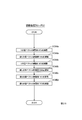
- FIG. 5 shows an adjustment processing flow P11 in which the controller 1410 of this embodiment controls the distortion compensation signal generation path 110.
- the adjustment process flow P11 includes adjustment of the third-order distortion vector adjuster 1240a (S1240a), adjustment of the sub-third-order distortion vector adjuster 1340a (S1340a), adjustment of the third-order distortion vector adjuster 1240b (S1240b), and sub-third-order distortion.
- the vector adjuster 1340b is adjusted (S1340b) in order.
- the controller 1410 is, for example, a perturbation method (“T. Nojima and T.
- ⁇ Adjustment of third-order distortion vector adjuster 1240a> (In case of perturbation method) A case where the perturbation method is used as a method of adjusting the phase value and the amplitude value given to the third-order distortion vector adjuster 1240a will be described.
- the controller 1410 designates power measurement in either the third-order distortion component upper band 3DU1 or the third-order distortion component lower band 3DL1 to the distortion observer 1420 so as to reduce the power in the band.
- the phase value and the amplitude value of the third-order distortion vector adjuster 1240a are respectively adjusted.
- phase value XP Specified before and after the arbitrarily set phase value XP (it does not have to be the same as the initial value in the adjustment of other third-order distortion vector adjusters 1240b and sub-third-order distortion vector adjusters 1340a and 1340b described later)
- the power PD in the band is measured, the phase is changed by a predetermined offset value ⁇ XP in the direction in which the power PD decreases, and the power PD is measured by the distortion observer 1420.
- the phase value XP MIN at which the power PD is equal to or less than a predetermined threshold value TH is obtained.
- the obtained phase value XP MIN is set in the third-order distortion vector adjuster 1240a.
- a quadratic function has been described as an example.
- the phase value with the lowest power among the measured powers can be defined as XP MIN. Good.
- the amplitude value is set after the phase value is set. However, when the sensitivity of the distortion component generated in the power amplifier 230 is higher than the phase value, the amplitude value is set. You may go first.
- R In order to specify a quadratic function using the least square method, R needs to be at least 3. However, since R can be approximated with higher accuracy by increasing R, it is within the range allowed by calculation conditions and other requirements. And R may be larger than 3. In addition, it is simplest to set R to the same number in setting the phase value and the amplitude value. However, if it is necessary to improve the approximation accuracy of either the phase value or the amplitude value, the setting of the phase value and the amplitude value is performed. R may be a different value.
- the third-order distortion vector adjuster 1240b and the sub-third-order distortion vector adjuster 1340b are adjusted by designating either the third-order distortion component upper band 3DU2 or the third-order distortion component lower band 3DL2
- the phase value and the amplitude value of the third-order distortion vector adjuster 1240b and the sub-third-order distortion vector adjuster 1340b are adjusted in the same procedure as the adjustment of the third-order distortion vector adjuster 1240a so as to reduce power.
- the value of R may be different from that of the third-order distortion vector adjuster 1240a depending on the required approximation accuracy.
- the processing time for setting the phase value and the amplitude value is longer than that in the calculation method using quadratic function approximation, but the distortion compensation amount of the predistorter may be increased.
- the phase value and the amplitude value can be set in a shorter time than the perturbation method.
- the setting of the phase value and the amplitude value may be appropriately selected according to the time required for processing and the required distortion compensation amount. In addition, either method may be selected instead of being selected.
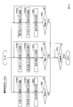
- FIG. 6 shows an adjustment processing flow P12 in which the controller 1410 of this embodiment controls the distortion compensation signal generation path 110.
- the distortion observer 1420 measures the power of each band of the distortion component (S901). . Determining power measured in band or all is below a predetermined threshold value P TH (S991). If the power of all the bands is equal to or less than the threshold value PTH , the adjustment process flow P12 is terminated. When the condition is not satisfied, the process returns to the adjustment (S1240a) of the third-order distortion vector adjuster 1240a. A series of repetition processing is repeated until the condition is satisfied in S991 or a predetermined number of times.
- the order of processing is adjusted by the sub third-order distortion vector adjuster 1340a from the viewpoint of reducing the number of repetitions (S1340a),
- the order of the adjustment of the third-order distortion vector adjuster 1240a (S1240a), the adjustment of the sub-third-order distortion vector adjuster 1340b (S1340b), and the adjustment of the third-order distortion vector adjuster 1240b (S1240b) may be used.
- adjustment of the third-order distortion vector adjuster 1240a (S1240a), adjustment of the third-order distortion vector adjuster 1240b (S1240b), adjustment of the sub-third-order distortion vector adjuster 1340a (S1340a), and sub-third-order distortion vector adjuster 1340b
- the order of adjustment (S1340b) may be used. Since the power amplifier may have different characteristics, confirm in advance in which order in the possible combinations it will reach the threshold PTH or less with the smallest number of iterations, and perform processing in that confirmed order It is good.
- Adjustment Processing Flow P13 of Embodiment 1 In the adjustment process flow P11 and the adjustment process flow P12, the adjustment from the third-order distortion vector adjuster 1240a to the sub-third-order distortion vector adjuster 1340b is performed in a predetermined order, but in parallel as in the adjustment process flow P13. It is good also as what is processed. When the influence due to the mutual dependence of the distortion components is small, there are cases where the processing can be made to be equal to or less than the threshold value PTH in a shorter processing time by performing the processing independently in parallel for each frequency band.
- FIG. 7 shows an adjustment processing flow P13 in which the controller 1410 of this embodiment controls the distortion compensation signal generation path 110.
- the adjustment processing flow P13 sequentially performs adjustment of the third-order distortion vector adjuster 1240a (S1240a) and adjustment of the sub-third-order distortion vector adjuster 1340a (S1340a), and the third-order distortion component lower band 3DL1 and the third-order distortion component upper side.
- Each power in the band 3DL1 is measured (S902). Determining power measured in band or all is below a predetermined threshold value P TH (S992).
- P TH predetermined threshold value
- the adjustment of the third-order distortion vector adjuster 1240b (S1240b) and the adjustment of the sub-third-order distortion vector adjuster 1340b (S1340b) are performed in order, and the third-order distortion component upper band 3DU2 and the third-order distortion component lower band 3DL2 Each power is measured (S903). Determining power measured in band or all is below a predetermined threshold value P TH (S993). When the condition is not satisfied, the process returns to the adjustment (S1240b) of the third-order distortion vector adjuster 1240b. When both the conditions are satisfied in S992 and S993, the adjustment processing flow P13 is terminated (S999).
- the threshold value P TH may be a single value or a threshold value may be set for each band.
- the threshold value of each band is set according to the required distortion component tolerance. It is desirable to set. The same applies to any embodiment or modification described below.
- the nonlinear characteristics of the power amplifier may depend on the average power or instantaneous power of the signal input to the power amplifier. Therefore, a lookup table that refers to the amplitude and phase given to the third-order distortion vector adjuster according to the average power or instantaneous power of the signal input to the power amplifier may be used.
- the average power is used as an index
- the amplitude and phase to be given to the third-order distortion vector adjuster are obtained in advance using the adjustment processing flow described above for each predetermined average power, and the amplitude and phase are associated with the average power. In the lookup table.
- the average power of the signal input to the predistorter is observed, and the amplitude and phase of the third-order distortion vector adjuster corresponding to the average power are used.
- the amplitude and phase of the third-order distortion vector adjuster can be changed according to the average power, there are cases where the distortion component can be compensated more than when the amplitude and phase are fixed. The same applies when referring to the amplitude and phase according to the instantaneous power.
- [Modification 1 of Example 1] In order to simplify the configuration of the distortion compensation signal generation path, it can be configured as in the following modification.
- the third-order distortion is replaced with the sub-third-order distortion generator 1320, the phase adjusters 1350a and 1350b, the combiner 1360, the sub-distributor 1330, and the sub-digital filters 1310a and 1310b.
- the calculator 1370 By including the calculator 1370, the number of parts can be reduced, and the configuration of the distortion compensation signal generation path can be simplified.
- FIG. 8 is a block diagram showing the overall configuration of the predistorter 11 and peripheral devices according to this modification.
- FIG. 9 is a block diagram showing a configuration of a distortion compensation signal generation path 111 provided in the predistorter 11 according to this modification.
- the predistorter 11 of this modification includes a distortion compensation signal generation path 111, a control section 140, a linear transmission path 150, a signal distribution section 161, a signal synthesis section 170, a DAC 180, and an ADC 190.
- the signal distributor 161 includes a distributor 1610 and a distributor 1621.
- the distortion compensation signal generation path 111 includes signal generation units 121 a and 121 b and a sub signal generation unit 131.
- the distributor 1621 distributes the input signal x (t) output from the distributor 1610 to the signal generators 121a and 121b.
- the signal generator 121a includes a digital filter 1210a, a distributor 1230a, a third-order distortion generator 1220a, and a third-order distortion vector adjuster 1240a.
- the digital filter 1210a passes only the component of the frequency band designated in advance among the input signal x (t) output from the distributing unit 1621 and generates the individual carrier input signal s 1 (t).
- the distributor 1230a distributes the individual carrier input signal s 1 (t) output from the digital filter 1210a to the sub-signal generator 131 and the third-order distortion generator 1220a.
- the third-order distortion generator 1220a generates the individual carrier distortion signal d A (t) by raising the individual carrier input signal s 1 (t) output from the distributor 1220a to the third power in order to generate a third-order distortion component.
- Third-order distortion vector adjuster 1240a adjusts the phase and amplitude of individual carrier distortion signal d A (t) output from third-order distortion generator 1220a on the basis of control information provided from controller 1410, thereby adjusting individual carrier distortion.
- a compensation signal is generated and output to the synthesis unit 1720.
- the signal generator 121b includes a digital filter 1210b, a distributor 1230b, a third-order distortion generator 1220b, and a third-order distortion vector adjuster 1240b.
- the digital filter 1210b passes only the component of the frequency band designated in advance among the input signal x (t) output from the distributing unit 1621 and generates the individual carrier input signal s 2 (t).
- the distributor 1230b distributes the individual carrier input signal s 2 (t) output from the digital filter 1210b to the sub-signal generator 131 and the third-order distortion generator 1220b.
- the third-order distortion generator 1220b generates the individual carrier distortion signal d B (t) by raising the individual carrier input signal s 2 (t) output from the distributor 1220b to the third power in order to generate a third-order distortion component.
- Third-order distortion vector adjuster 1240b adjusts the phase and amplitude of individual carrier distortion signal d B (t) output from third-order distortion generator 1220b based on the control information provided from controller 1410, and thereby adjusts the individual carrier distortion.
- a compensation signal is generated and output to the synthesis unit 1720.
- the sub-signal generator 131 includes a third-order distortion calculator 1370 and sub-third-order distortion vector adjusters 1340a and 1340b.
- Third-order distortion calculator 1370 calculates carrier intermodulation distortion signal d CA (t) from individual carrier input signal s 1 (t) output from distributor 1230a and individual carrier input signal s 2 (t) output from distributor 1230b.
- D CB (t) are generated and output to the sub third-order distortion vector adjusters 1340a and 1340b, respectively.
- 2 s 1 (t) and d CB (t) 2
- the sub-third-order distortion vector adjuster 1340a adjusts the phase and amplitude of the carrier intermodulation distortion signal d CA (t) output from the third-order distortion calculator 1370 based on the control information provided from the controller 1410, and performs mutual adjustment.
- a carrier distortion compensation signal is generated and output to the synthesis unit 1720.
- the sub-third-order distortion vector adjuster 1340b adjusts the phase and amplitude of the carrier intermodulation distortion signal d CB (t) output from the third-order distortion calculator 1370 based on the control information given from the controller 1410, so A carrier distortion compensation signal is generated and output to the synthesis unit 1720.
- the adjustment process flow in which the controller 1410 of this modification controls the distortion compensation signal generation path 111 is the same as that in the first embodiment.
- the frequency band as an example can correspond by also above concept for the case where the the N B 3 above. More specifically, for example, if the first embodiment, to prepare the N B number of signal generating portion to the distortion compensation signal generation path 110.
- the individual carrier distortion signal output from the third-order distortion generator included in each signal generator is adjusted by the phase adjuster and combined with the carrier intermodulation distortion signal output from the sub-third-order distortion generator 1320 included in the sub-signal generation section 130. To do. Since it can be calculated from the above equation (3) which frequency band the distortion component is generated, sub digital filters are prepared for the number of distortion components generated in the same frequency band as the input signal, and the signal output from the combiner 1360 is output.
- a signal to be passed is taken out, and the phase and amplitude are adjusted by the sub third-order distortion vector adjuster 1340.
- a third-order distortion calculator 1370 is prepared as in the distortion compensation signal generation path 111 in the first embodiment, the distortion component generated in the same frequency band as the input signal is generated by calculation, and the same frequency as the input signal is generated.
- Sub-third order distortion vector adjusters are provided for the number of distortion components generated in the band, and the phase and amplitude of the carrier intermodulation distortion signal output from the third order distortion calculator 1370 are adjusted by the sub third order distortion vector adjuster. May be.
- FIG. 11 is a block diagram showing the overall configuration of the predistorter 12 and peripheral devices according to this modification.
- FIG. 12 is a block diagram showing the configuration of the distortion compensation signal generation path 112 provided in the predistorter 12 according to this modification.
- FIG. 13 is a block diagram showing the configuration of the third-order distortion frequency characteristic compensator 1290.
- the predistorter 12 of this modification includes a distortion compensation signal generation path 112, a control unit 141, a linear transmission path 150, a signal distribution unit 160, a signal synthesis unit 170, a DAC 180, and an ADC 190.
- the distortion compensation signal generation path 112 includes signal generation units 122 a and 122 b and a sub signal generation unit 132.
- the signal generator 122a includes a digital filter 1210a, a third-order distortion generator 1220a, a distributor 1230a, a third-order distortion vector adjuster 1240a, and a third-order distortion frequency characteristic compensator 1290a.
- the third-order distortion frequency characteristic compensator 1290a includes a third-order distortion component lower band 3DL1 and a third-order distortion component upper band 3DU1 as shown in FIG. 10 among the individual carrier distortion compensation signals output from the third-order distortion vector adjuster 1240a.
- M bands f 1 ,..., F M
- the phase and amplitude of the individual carrier distortion compensation signal output from the third-order distortion vector adjuster 1240a are adjusted for each divided band.
- the third-order distortion frequency characteristic compensator 1290a includes a serial-parallel converter 12910, a K-point FFT (Fast Fourier Transform) 12920, and K complex multipliers 12930 1 to 12930 K and K-point IFFT (Inverse Fast Fourier Transform) 12940. And a parallel-serial converter 12950.
- the serial-parallel converter 12910 converts the individual carrier distortion compensation signal output from the third-order distortion vector adjuster 1240a into serial-parallel conversion for every K samples.
- the K-point FFT unit 12920 performs fast Fourier transform for each K samples (K is a predetermined integer greater than M), and the signal output from the serial / parallel conversion unit 12910 shown in the time domain is displayed in the frequency domain. Convert. Signals corresponding to the divided bands f 1 of the signal outputted from the K-point FFT unit 12920 is input to the complex multiplier twelve thousand nine hundred and thirty k corresponding to the divided band f 1 (1 ⁇ k ⁇ K ). Then, based on the phase value and amplitude value given from the controller 1411, the phase and amplitude of the signal input to the complex multiplier 12930 k corresponding to the divided band f 1 are respectively adjusted. The same applies to the divided bands f 2 to f M.
- the output of the K-point FFT unit 12920 that does not correspond to any of the divided bands (the output corresponding to the band lower than the divided band f 1 and the output corresponding to the band higher than the divided band f M shown in FIG. 10).
- the band between the third-order distortion component lower band 1 and the third-order distortion component upper band 1) are input to the K-point IFFT unit 12940 without adjusting the phase and amplitude by the complex multiplier.
- the K-point IFFT unit 12940 converts K signals output from the complex multipliers 12930 1 to 12930 K shown in the frequency domain into the time domain.
- the parallel-serial conversion unit 12950 performs parallel-serial conversion for every K samples.
- the phase value and the amplitude value given to the complex multipliers 12930 1 to 12930 K corresponding to the divided bands f 1 to f M are calculated using the perturbation method or quadratic function approximation, similar to the adjustment of the third-order distortion vector adjuster 1240a. Set according to the law.
- the difference from the adjustment of the third-order distortion vector adjuster 1240a is that the band for measuring the power of the distortion component measured by the distortion observer 1421 is the power in the divided band for adjusting the phase value or the amplitude value. For example, when adjusting a phase value and an amplitude value of the complex multiplier 12930 k corresponding to the divided bands f 1, to measure the power in the divided band f 1 by distortion observer 1421.
- the phase value and the amplitude value to be given to the complex multipliers 12930 1 to 12930 K may be set in order from the divided bands f 1 to f M. At this time, the setting of the phase value and the amplitude value corresponding to the divided bands f 1 to f M may be repeated until the level of the distortion component becomes equal to or less than the threshold value P TH . Further, the order of the divided bands for setting the phase value and the amplitude value may be changed according to the characteristics of the power amplifier 230. For example, a subband with a high distortion component level may have a greater effect on other bands than a subband with a low level. Therefore, it is repeated by setting in order from the subband with the highest distortion component level. The number of times may be reduced.
- phase values or amplitude values of a plurality of divided bands or all divided bands may be set simultaneously.
- the time required for setting can be shortened by simultaneously setting the phase value or the amplitude value.
- the above description is about the third-order distortion frequency characteristic compensator 1290a for the signal s 1 (t) in the first frequency band SB1.
- the third-order distortion frequency characteristic compensator 1290b for the signal s 2 (t) in the second frequency band SB2 has the same configuration as the third-order distortion frequency characteristic compensator 1290a shown in FIG. 13, and performs the same operation. However, the configuration diagram and description thereof are omitted.
- FIG. 14 shows an adjustment processing flow P14 in which the controller 1411 of this modification controls the distortion compensation signal generation path 112.
- the adjustment process flow P14 includes adjustment of the third-order distortion vector adjuster 1240a (S1240a), adjustment of the third-order distortion frequency characteristic compensator 1290a (S1290a), adjustment of the sub-third-order distortion vector adjuster 1340a (S1340a), and sub-third-order.
- Adjustment of distortion frequency characteristic compensator 1390a (S1390a), adjustment of third order distortion vector adjuster 1240b (S1240b), adjustment of third order distortion frequency characteristic compensator 1290b (S1290b), adjustment of sub third order distortion vector adjuster 1340b ( S1340b) and the adjustment (S1390b) of the sub third-order distortion frequency characteristic compensator 1390b are performed in order.
- the distortion observer 1421 measures the power of each band of the distortion component, and the measured band It is also possible to repeat until all the electric power within becomes equal to or less than a predetermined threshold value PTH .
- the third-order distortion frequency characteristic compensator compensates for the distortion component after the third-order distortion vector adjuster compensates for the distortion component.
- the power in all the bands may be less than or equal to the threshold value PTH with a smaller number of repetitions. Therefore, the adjustment process flow of the controller 1411 may be an adjustment process flow P15 described below.
- FIG. 15 shows an adjustment processing flow P15 in which the controller 1411 of this modification controls the distortion compensation signal generation path 112.
- the adjustment process flow P15 includes adjustment of the third-order distortion vector adjuster 1240a (S1240a), adjustment of the sub-third-order distortion vector adjuster 1340a (S1340a), adjustment of the third-order distortion frequency characteristic compensator 1290a (S1290a), and sub-third order.
- Adjustment of distortion frequency characteristic compensator 1390a (S1390a), adjustment of third order distortion vector adjuster 1240b (S1240b), adjustment of sub third order distortion vector adjuster 1340b (S1340b), adjustment of third order distortion frequency characteristic compensator 1290b ( S1290b) and the adjustment (S1390b) of the sub-third-order distortion frequency characteristic compensator 1390b are sequentially performed. Thereafter, the distortion observer 1421 measures the power of each band of the distortion component (S901). Determining power measured in band or all is below a predetermined threshold value P TH (S991). If the power of all the bands threshold P TH or less, and terminates the adjustment process P15. When the condition is not satisfied, the process returns to the adjustment (S1240a) of the third-order distortion vector adjuster 1240a. A series of repetition processing is repeated until the condition is satisfied in S991 or a predetermined number of times.
- Adjustment Process Flow P16 of Modification 2 of Embodiment 1 For the same reason as the adjustment process flow P15 of the second modification of the first embodiment, the adjustment process flow of the controller 1411 may be configured as an adjustment process flow P16 described below.
- FIG. 16 shows an adjustment processing flow P16 in which the controller 1411 of this modification controls the distortion compensation signal generation path 112.
- the adjustment processing flow P16 includes adjustment of the third-order distortion vector adjuster 1240a (S1240a), adjustment of the sub-third-order distortion vector adjuster 1340a (S1340a), adjustment of the third-order distortion vector adjuster 1240b (S1240b), and sub-third-order distortion.
- Adjustment of vector adjuster 1340b Adjustment of third-order distortion frequency characteristic compensator 1290a (S1290a) Adjustment of sub-third-order distortion frequency characteristic compensator 1390a (S1390a) Adjustment of third-order distortion frequency characteristic compensator 1290b ( S1290b) and the adjustment (S1390b) of the sub-third-order distortion frequency characteristic compensator 1390b are sequentially performed. Thereafter, the distortion observer 1421 measures the power of each band of the distortion component (S901). Determining power measured in band or all is below a predetermined threshold value P TH (S991). If the power of all the bands is equal to or less than the threshold value PTH , the adjustment process flow P16 is terminated. When the condition is not satisfied, the process returns to the adjustment (S1240a) of the third-order distortion vector adjuster 1240a. A series of repetition processing is repeated until the condition is satisfied in S991 or a predetermined number of times.
- Adjustment Process Flow P17 of Modification 2 of Embodiment 1 the adjustment process flow of the controller 1411 may be configured as an adjustment process flow P17 described below.
- FIG. 17 shows an adjustment processing flow P17 in which the controller 1411 of this modification controls the distortion compensation signal generation path 112.
- the adjustment process flow P17 includes adjustment of the third-order distortion vector adjuster 1240a (S1240a), adjustment of the third-order distortion frequency characteristic compensator 1290a (S1290a), adjustment of the sub-third-order distortion vector adjuster 1340a (S1340a), and sub-third-order.
- the distortion frequency characteristic compensator 1390a is adjusted (S1390a) in order, and the power in the third-order distortion component upper band 3DU1 and the third-order distortion component lower band 3DL1 is measured (S902). Determining power measured in band or all is below a predetermined threshold value P TH (S992).
- the process returns to the adjustment (S1240a) of the third-order distortion vector adjuster 1240a.
- adjustment of third-order distortion vector adjuster 1240b (S1240b) adjustment of third-order distortion frequency characteristic compensator 1290b (S1290b), adjustment of sub-third-order distortion vector adjuster 1340b (S1340b), sub-third-order distortion frequency characteristic compensation
- the device 1390b is adjusted (S1390b) in order, and the power in the third-order distortion component upper band 3DU2 and the third-order distortion component lower band 3DL2 is measured (S903). Determining power measured in band or all is below a predetermined threshold value P TH (S993).
- P TH predetermined threshold value
- the third-order distortion vector adjuster 1240a is adjusted (S1240a), the sub-third-order distortion vector adjuster 1340a is adjusted (S1340a), and the third-order distortion frequency characteristics.
- the adjustment of the compensator 1290a (S1290a) and the adjustment of the sub third-order distortion frequency characteristic compensator 1390a (S1390a) may be performed in order.
- adjustment of the third-order distortion vector adjuster 1240b (S1240b), adjustment of the sub-third-order distortion vector adjuster 1340b (S1340b), adjustment of the third-order distortion frequency characteristic compensator 1290b (S1290b), and sub-third-order distortion frequency characteristic compensation may be performed in order.
- the third-order distortion frequency characteristic compensator is installed at the subsequent stage of all the third-order distortion vector adjusters.
- the frequency dependence of the specific distortion component is small. Is done.
- the sub-third-order distortion frequency characteristic compensator 1390b may not be installed.
- FIG. 18 is a block diagram showing the overall configuration of the predistorter 13 and peripheral devices according to this embodiment.
- FIG. 19 is a block diagram illustrating a configuration of a distortion compensation signal generation path 113 provided in the predistorter 13 according to the present embodiment.
- the peripheral devices of this embodiment are a signal generator 40, an amplifier 21, a feedback signal generator 30, and an output terminal 50.
- the predistorter 13 of this embodiment includes a distortion compensation signal generation path 113, a control section 140, linear transmission paths 151a and 151b, a signal distribution section 162, a signal synthesis section 171, a DAC 180a, a DAC 180b, and an ADC 190.
- the signal distributor 162 includes a distributor 1611 and a distributor 1620.
- the distributor 1611 distributes the input signal output from the signal generator 40 to the linear transmission paths 151 a and 150 b and the distortion compensation signal generation path 113.
- the linear transmission path 151a includes a delay device 1510a and a digital filter 1520a.
- the digital filter 1520a passes the signal using the first frequency band among the input signals output from the signal distributor 1611 and generates the individual carrier input signal s 1 (t).
- the delay unit 1510a delays the individual carrier input signal s 1 (t) output from the digital filter 1520a so as to coincide with the delay time of the distortion compensation signal input to the signal adder 1710a via the distortion compensation signal generation path 113.
- the linear transmission path 151b includes a delay unit 1510b and a digital filter 1520b.
- the digital filter 1520b passes the signal using the second frequency band among the input signals output from the signal distributor 1611, and generates the individual carrier input signal s 2 (t).
- the delay unit 1510b delays the individual carrier input signal s 2 (t) output from the digital filter 1520b so as to coincide with the delay time of the distortion compensation signal input to the signal adder 1710b via the distortion compensation signal generation path 113.
- the signal synthesis unit 171 includes adders 1710a and 1710b and synthesis units 1720a and 1720b.
- the adder 1710a combines the signal output from the linear transmission path 151a and the signal output from the combining unit 1720a.
- the adder 1710b combines the signal output from the linear transmission path 151b and the signal output from the combining unit 1720b.
- the combining units 1720a and 1720b will be described in the description of the distortion compensation signal generation path 113 described later.
- the DAC 180a converts the digital signal output from the signal adder 1710a into an analog signal.
- the DAC 180b converts the digital signal output from the signal adder 1710b into an analog signal.
- the amplification device 21 includes quadrature modulators 210a and 210b, up-converters 220a and 220b, a power amplifier 230, and a power combiner 240.
- the quadrature modulator 210a performs quadrature modulation on the analog signal output from the DAC 180a.
- the quadrature modulator 210b performs quadrature modulation on the analog signal output from the DAC 180b.
- the up-converter 220a up-converts the signal output from the quadrature modulator 210a to a target frequency.
- up-converter 220b up-converts the signal output from quadrature modulator 210b to a target frequency.
- the power combiner 240 combines the signals output from the up-converters 220a and 220b.
- the power amplifier 230 amplifies the signal output from the power combiner 240 to a target power.
- the outputs of the quadrature modulators 210a and 210b are combined by the power combiner 240 and the output is A configuration in which up-conversion is performed by one up-converter may be employed.
- the signal delay time is adjusted to be the same.
- the distortion compensation amount deteriorates because a difference occurs between the distortion compensation signal generated by the predistorter 13 and the distortion component generated by the power amplifier 230.
- the frequency domain is converted to the time domain by inverse fast Fourier transform.
- downsampling is performed so as to obtain a predetermined sampling rate.
- the downsampled signal is input to the DAC 180b.
- Upconverter 220b up-converts the output of DAC180b passing through the quadrature modulator 210b to F c2.
- downsampling is performed so that a predetermined sampling rate is obtained between the signal adder 1710a and the DAC 180a, and the downsampled signal is input to the DAC 180a.
- the up-converter 220a up-converts the output of the DAC 180a that has passed through the quadrature modulator 210a to F c1 . Thereby, the sampling rate of the DAC can be lowered, and an increase in power consumption due to an increase in the sampling rate can be avoided.
- the configuration using a plurality of DACs may be configured in this manner.
- the distortion compensation signal generation path 113 includes a signal generation unit 120a, a signal generation unit 120b, and a sub-signal generation unit 130.
- the combining unit 1720a generates a distortion compensation signal by combining the signals output from the third-order distortion vector adjuster 1240a included in the signal generation unit 120a and the sub-third-order distortion vector adjuster 1340a included in the sub-signal generation unit 130. Output to the signal adder 1710a.
- the above-described combining unit 1720b combines the signals output from the third-order distortion vector adjuster 1240b included in the signal generation unit 120b and the sub-third-order distortion vector adjuster 1340b included in the sub-signal generation unit 130, thereby compensating for distortion.
- a signal is generated and output to the signal adder 1710b.
- the adjustment processing flow in which the controller 1410 of this embodiment controls the distortion compensation signal generation path 113 is the same as that of the first embodiment.
- the difference between the predistorter 14 of the present modification and the predistorter 13 of the second embodiment is that the number of frequency bands includes ADCs and distortion observers, and the controller refers to the measurement results of each distortion observer. That is.
- the difference in the feedback signal generator is that it includes a power distributor that distributes the output signal from the directional coupler, and that there are as many downconverters and quadrature demodulators as the number of frequency bands.
- FIG. 20 is a block diagram showing the overall configuration of the predistorter 14 and peripheral devices according to this modification.
- FIG. 21 is a block diagram showing a configuration of a distortion compensation signal generation path 114 provided in the predistorter 14 according to this modification.
- Peripheral devices of this modification are a signal generator 40, an amplifier 21, a feedback signal generator 31, and an output terminal 50.
- the predistorter 14 of the present modification includes a distortion compensation signal generation path 114, a control section 142, linear transmission paths 151a and 151b, a signal distribution section 161, a signal synthesis section 171, a DAC 180a, a DAC 180b, an ADC 190a, and an ADC 190b.
- the feedback signal generator 31 includes a directional coupler 310, down converters 320a and 320b, quadrature demodulators 330a and 330b, and a power distributor 340.
- the power distributor 340 distributes the feedback signal output from the directional coupler 310 to the down converter 320a and the down converter 320b.
- the down converter 320a down-converts the signal output from the directional coupler 310 to a predetermined frequency.
- the down-converter 320a passes only a signal using the first frequency band.
- the down converter 320b down-converts the feedback signal output from the directional coupler 310 to a predetermined frequency.
- the down-converter 320b passes only a signal using the second frequency band.
- the quadrature demodulator 330a demodulates the signal output from the down converter 320a into an I-phase signal and a Q-phase signal.
- quadrature demodulator 330b demodulates the signal output from down converter 320b into an I-phase signal and a Q-phase signal.
- the output of the directional coupler 310 is received with only one down converter 320, and the output of the down converter 320 is distributed to the quadrature demodulators 330a and 330b by the distributor 340.
- the number of parts may be reduced.
- the control unit 142 includes strain observers 1422a and 1422b and a controller 1412.
- the distortion observer 1422a observes a distortion component generated in the vicinity of the first frequency band, and transmits the measurement result to the controller 1412.
- the distortion observer 1422b observes a distortion component generated in the vicinity of the second frequency band, and transmits the measurement result to the controller 1412.
- the distortion observers 1422a and 1422b may be configured by analog circuits.
- the configurations of the distortion observers 1422a and 1422b for example, the number of frequency bands for which power is desired to be measured, two band-pass filters and two power measuring instruments can be used.
- the ADC 190a is installed between the strain observer 1422a and the controller 1412
- the ADC 190b is installed between the strain observer 1422b and the controller 1412.
- the distortion observer 1422a passes only the signal of the frequency band whose power is to be measured by the band pass filter with respect to the feedback signal output from the quadrature demodulator 330a, and measures the power of the signal output from the band pass filter by the power meter. To do.
- the measurement result is transmitted to the controller 1412 via the ADC 190. At this time, if power in a desired frequency band can be measured from the signal output from the down converter 320a, the quadrature demodulator 330a may not be used.
- the distortion observer 1422b passes only the signal in the frequency band whose power is to be measured by the bandpass filter with respect to the signal output from the down converter 320b or the feedback signal output from the quadrature demodulator 330b, and the bandpass filter Measure the power of the output signal with a power meter.
- the measurement result is transmitted to the controller 1412 via the ADC 190b. At this time, if power in a desired frequency band can be measured from the signal output from the down converter 320b, the quadrature demodulator 330b may not be used.
- the difference between the predistorter 15 of this modification and the predistorter 13 (FIG. 18) of the second embodiment is that two signal generators 40a and 40b and two signal distributors 1610a and 1610b are used. In other words, signals in two frequency bands are separately input to the distortion compensation signal generation path 115.
- the difference from the distortion compensation signal generation path 113 (FIG. 19) is that the distribution unit 1622 includes two distributors 1630 a and 1630 b and a combiner 1640.
- FIG. 22 is a block diagram showing the overall configuration of the predistorter 15 and peripheral devices according to this modification.
- FIG. 23 is a block diagram showing a configuration of a distortion compensation signal generation path 115 provided in the predistorter 15 according to this modification.
- Peripheral devices of this modification are signal generators 40 a and 40 b, an amplifier 21, a feedback signal generator 30, and an output terminal 50.
- the signal generators 40a and 40b respectively generate a signal in the first frequency band and a signal in the second frequency band, and supply them to the distributors 1610a and 1610b, respectively.
- both signal generators 40a and 40b may be baseband signals.
- the processing speed of the signal processing unit can be reduced, and a predistorter can be realized by a signal processing unit such as a DSP (digital signal processor) or FPGA (field programmable array) having a low operation clock.
- the up-converter 220b sets the center frequency of the signal output from the DAC 180b that has passed through the quadrature modulator 210b to a predetermined frequency interval with respect to the center frequency of the signal output from the up-converter 220a.
- the predistorter 15 of this modification includes a distortion compensation signal generation path 115, a control unit 140, linear transmission paths 150a and 150b, a signal distribution unit 163, a signal synthesis unit 171, a DAC 180a, a DAC 180b, and an ADC 190.
- the signal distributor 163 includes distributors 1610 a and 1610 b and a distributor 1622.
- the signal distributor 1610a distributes the input signal output from the signal generator 40a to the linear transmission path 150a and the distortion compensation signal generation path 115.
- the signal distributor 1610b distributes the input signal output from the signal generator 40b to the linear transmission path 150b and the distortion compensation signal generation path 115.
- the distributor 1622 includes a distributor 1630a, a distributor 1630b, and a combiner 1640.
- the distributor 1630a distributes the input signal output from the signal distributor 1610a to the signal generator 120a and the combiner 1640.
- distributor 1630b distributes the input signal output from signal distributor 1610b to signal generator 120b and combiner 1640.
- the combiner 1640 combines the signal output from the distributor 1630a and the signal output from the distributor 1630b and outputs the combined signal to the sub-signal generator 130.
- the linear transmission path 150a includes a delay unit 1510a.
- the delay unit 1510a outputs a signal output from the signal distributor 1610a so that the delay time of the output of the delay unit 1510a matches the delay time of the distortion compensation signal input to the signal adder 1710a via the distortion compensation signal generation path 115.
- Delay Similarly, the linear transmission path 150b includes a delay device 1510b.
- the delay unit 1510b outputs a signal output from the signal distributor 1610b so that the delay time of the output of the delay unit 1510b matches the delay time of the distortion compensation signal input to the signal adder 1710b via the distortion compensation signal generation path 115. Delay.
- the power amplifier Distortion components are generated not only in the vicinity of the band of the signal S1 and in the vicinity of the band of the signal S2, but are also generated at frequencies separated by the frequency interval of the signal with respect to the center frequency of each signal. For example, when the frequency interval between the signal 1 and the signal 2 is 100 MHz, distortion components are respectively generated at a frequency that is 100 MHz lower than the center frequency of the signal 1 and a frequency that is 100 MHz higher than the center frequency of the signal 2.
- this distortion component is normally suppressed by a radio circuit such as a duplexer (not shown) via an output terminal.
- a radio circuit such as a duplexer (not shown)
- adding a radio circuit to suppress the distortion component increases the loss from the output terminal to the antenna, and adds a radio circuit. Therefore, the problem that cost and a circuit scale increase arises.
- the components that compensate for these distortion components are suppressed by the sub digital filters 1310a and 1310b, respectively. In order to solve this problem, it can be configured as in the third embodiment.
- FIG. 24 is a block diagram showing the overall configuration of the predistorter 16 and peripheral devices according to this embodiment.
- FIG. 25 is a block diagram illustrating a configuration of a distortion compensation signal generation path 116 provided in the predistorter 16 according to the present embodiment.
- the predistorter 16 of this embodiment includes a distortion compensation signal generation path 116, a control unit 143, a linear transmission path 150, a signal distribution unit 160, a signal synthesis unit 170, a DAC 180, and an ADC 190.
- the control unit 143 includes a controller 1413 and a strain observer 1423.
- the distortion observer 1423 includes not only the distortion components in the vicinity of the signal S1 and in the vicinity of the signal S2 from the signal output from the ADC 190, but also the distortion component generated from the signal S1 at a frequency lower by the frequency interval between the signals S1 and S2 and the signal from the signal S2.
- the power of the distortion component generated at a frequency higher by the frequency interval between S1 and signal S2 can be measured with a predetermined bandwidth. Since these latter two distortion components do not include the components to be transmitted via the antenna, the frequencies of these distortion components are respectively centered, for example, the third-order distortion component lower band shown in FIG. It is preferable to measure power in the same bandwidth as from the lower end of 3DL1 to the upper end of third-order distortion component upper band 3DU1.
- the distortion compensation signal generation path 116 includes signal generation units 120 a and 120 b and a sub signal generation unit 133.
- the sub-signal generating unit 133 includes a sub-third-order distortion generator 1320, a phase adjuster 1350a, a phase adjuster 1350b, a combiner 1360, a sub-distributor 1331, sub-digital filters 1310a, 1310b, 1310c, 1310d, and a sub-third-order distortion vector. It includes regulators 1340a, 1340b, 1340c, 1340d.
- the sub distributor 1331 distributes the signal output from the combiner 1360 to the sub digital filters 1310a, 1310b, 1310c, and 1310d.
- the sub digital filter 1310c passes a signal corresponding to a distortion component generated at a frequency lower than the center frequency of the signal S1 by the frequency interval between the signal S1 and the signal S2, and generates a subcarrier intermodulation distortion signal. It is assumed that the bandwidth that the sub-digital filter 1310c passes is determined in advance.
- Sub-third-order distortion vector adjuster 1340c adjusts the phase and amplitude of the sub-carrier intermodulation distortion signal output from sub-digital filter 1310c based on the control information provided from controller 1413, thereby adjusting the sub-carrier inter-modulation distortion compensation signal. Is generated and output to the combining unit 1721.
- the sub digital filter 1310d passes a signal corresponding to a distortion component generated at a frequency higher than the center frequency of the signal S2 by the frequency interval between the signal S1 and the signal S2, and generates a subcarrier intermodulation distortion signal. It is assumed that the bandwidth through which the sub digital filter 1310d passes is also determined in advance.
- the sub third-order distortion vector adjuster 1340d adjusts the phase and amplitude of the subcarrier intermodulation distortion signal output from the sub digital filter 1310d based on the control information given from the controller 1413, thereby adjusting the subcarrier intermodulation distortion compensation signal. Is generated and output to the combining unit 1721.
- the synthesizer 1721 synthesizes the signals output from the third-order distortion vector adjusters 1240a and 1240b and the sub-third-order distortion vector adjusters 1340a, 1340b, 1340c, and 1340d, generates a distortion compensation signal, and supplies the signal to the signal adder 1710. Output.
- FIG. 26 shows an adjustment processing flow P31 in which the controller 1413 of this embodiment controls the distortion compensation signal generation path 116.
- the adjustment process flow P31 includes adjustment of the third-order distortion vector adjuster 1240a (S1240a), adjustment of the sub-third-order distortion vector adjuster 1340a (S1340a), adjustment of the third-order distortion vector adjuster 1240b (S1240b), and sub-third-order distortion.
- the adjustment of the vector adjuster 1340b (S1340b), the adjustment of the sub-third-order distortion vector adjuster 1340c (S1340c), and the adjustment of the sub-third-order distortion vector adjuster 1340d (S1340d) are sequentially performed.
- the adjustment of the sub third-order distortion vector adjuster 1340c refers to the result of measuring the power of the distortion component generated by the power amplifier 230 corresponding to the signal output from the sub digital filter 1310c with the distortion observer 1423, and the third-order distortion vector.
- the phase value and the amplitude value are adjusted respectively in the same procedure as the adjustment of the adjuster 1240a.
- the adjustment of the sub third-order distortion vector adjuster 1340d refers to the result of measuring the distortion component power generated by the power amplifier 230 corresponding to the signal output from the sub digital filter 1310d with the distortion observer 1423.
- the phase value and the amplitude value are respectively adjusted in the same procedure as the adjustment of the next distortion vector adjuster 1240a.
- the adjustment process flow of the controller 1413 may be configured as an adjustment process flow P32.
- FIG. 27 shows an adjustment processing flow P32 in which the controller 1413 of this embodiment controls the distortion compensation signal generation path 116.
- the distortion observer 1423 measures the power of each band of the distortion component (S904). . Determining power measured in band or all is below a predetermined threshold value P TH (S994). If the power of all the bands threshold P TH or less, and terminates the adjustment process P32. When the condition is not satisfied, the process returns to the adjustment (S1240a) of the third-order distortion vector adjuster 1240a. A series of repetition processing is repeated until the condition of S994 is satisfied or a predetermined number of times.
- the distortion observer 1423 in addition to the power of each band of the distortion component, the distortion observer 1423 generates the power within the distortion component band generated at a frequency lower than the center frequency of the signal S1 by the frequency interval between the signal S1 and the signal S2, and the center of the signal S2.
- the power in the distortion component band generated at a frequency higher than the frequency by the frequency interval between the signal S1 and the signal S2 is measured.
- FIG. 28 shows an adjustment processing flow P330 in which the controller 1413 of this embodiment controls the distortion compensation signal generation path 116.
- the adjustment process flow P33 includes adjustment of the third-order distortion vector adjuster 1240a (S1240a), adjustment of the sub-third-order distortion vector adjuster 1340a (S1340a), adjustment of the third-order distortion vector adjuster 1240b (S1240b), and sub-third-order distortion.
- the vector adjuster 1340b is adjusted (S1340b) in order, and the powers of the third-order distortion component upper band 3DU1, the third-order distortion component lower band 3DL1, the third-order distortion component upper band 3DU2, and the third-order distortion component lower band 3DL2, respectively. Measure (S905).
- Determining power measured in band or all is below a predetermined threshold value P TH (S995).
- the process returns to the adjustment (S1240a) of the third-order distortion vector adjuster 1240a.
- the adjustment of the sub third-order distortion vector adjuster 1340c (S1340c) and the adjustment of the sub-third order distortion vector adjuster 1340d (S1340d) are performed in order, and the frequency is lower than the center frequency of the signal S1 by the frequency interval between the signals S1 and S2.
- the power in the distortion component band generated at a frequency higher than the center frequency of the signal S2 by the frequency interval between the signals S1 and S2 are measured (S906).
- FIG. 29 shows an adjustment processing flow P34 in which the controller 1413 of this embodiment controls the distortion compensation signal generation path 116.
- the adjustment process flow P34 sequentially performs adjustment of the third-order distortion vector adjuster 1240a (S1240a) and adjustment of the sub-third-order distortion vector adjuster 1340a (S1340a) in order, and the third-order distortion component upper band 3DU1 and the third-order distortion component lower side
- the power of band 3DL1 is measured (S902). Determining power measured in band or all is below a predetermined threshold value P TH (S992).
- P TH predetermined threshold value
- the third-order distortion vector adjuster 1240b (S1240b) and the sub-third-order distortion vector adjuster 1340b are adjusted in order (S1340b), and the third-order distortion component upper band 3DU2 and the third-order distortion component lower band 3DL2 are adjusted.
- Each power is measured (S903). Determining power measured in band or all is below a predetermined threshold value P TH (S993). When the condition is not satisfied, the process returns to the adjustment (S1240b) of the third-order distortion vector adjuster 1240b.
- the adjustment of the sub third-order distortion vector adjuster 1340c (S1340c) and the adjustment of the sub-third order distortion vector adjuster 1340d (S1340d) are performed in order, and the frequency is lower by the frequency interval between the signal S1 and the signal S2 And the power in the distortion component band generated at a frequency higher than the center frequency of the signal S2 by the frequency interval between the signals S1 and S2 are measured (S906). Determining power measured in band or all is below a predetermined threshold value P TH (S996). When the condition is not satisfied, the process returns to the adjustment (S1340c) of the sub third-order distortion vector adjuster 1340c. When all the conditions are satisfied in S992, S993, and S996, the adjustment process flow P34 is ended (S999).
- the adjustment of the sub-third-order distortion vector adjuster 1340c (S1340c) and the adjustment of the sub-third-order distortion vector adjuster 1340d (S1340d) may be performed in parallel.
- the sub third-order distortion vector adjuster 1340c is adjusted (S1340c) to measure and measure the power in the distortion component band generated at a frequency lower than the center frequency of the signal S1 by the frequency interval between the signal S1 and the signal S2. It is determined whether the power in the determined band is equal to or less than a predetermined threshold value PTH .
- the process returns to the adjustment (S1340c) of the sub third-order distortion vector adjuster 1340c.
- the case where the center frequencies of the signal S1 and the signal S2 are separated as shown in FIG. 4 has been described.
- the center frequencies of the signal S1 and the signal S2 are close to each other, that is, the bands of the signal S1 and the signal S2 are continuous.
- the same idea can be applied to the case.
- the distortion component generated in the same band as the signal S1 or in a frequency lower than the signal S1 is compensated, the distortion component of 3DU1 in FIG. 10 is generated in the same band as the signal S1, and thus the distortion component of 3DU1 is not observed.
- the distortion component is observed only in the 3DL1 band.
- a distortion component is generated only in the 3DL1 band, for example, an indicator such as EVM (error vector ⁇ magnitude) of the signal S2 is observed, and the amplitude and phase of the signal that compensates for the distortion component are adjusted so as to improve the EVM. Good.
- EVM error vector ⁇ magnitude
- the distortion component of 3DL2 is the same band as the signal S1, and thus cannot be observed. Therefore, only the distortion component in the band of 3DU2 Observe.
- the distortion components cannot be compensated for when the bands passed by the sub digital filters 1310a and 1310c overlap, it is not a configuration using the sub digital filters 1310a, 1310b, 1310c, and 1310d, but the center of the signal S1 is not provided in the third order distortion calculator. It is desirable to have a function of generating a distortion component generated at a frequency lower than the frequency by the frequency interval between the signal S1 and the signal S2. The same applies when the bands passed by the sub digital filters 1310b and 1310d overlap.
- the difference between the predistorter 17 of the present modification and the predistorter 16 of the third embodiment is that two DACs are added, the output of the distortion compensation signal generation path 117 is three, and the distortion compensation signal generation path Are output to different DACs.
- the difference between the amplifying devices is that quadrature modulators 210 and up-converters 220 corresponding to the number of DACs are provided, a power combiner 240 that combines the outputs of the up-converter 220 is included, and a signal that has passed through the power combiner 240 is received. Output to the power amplifier 230.
- FIG. 30 is a block diagram showing the overall configuration of the predistorter 17 and peripheral devices according to this modification.
- FIG. 31 is a block diagram showing a configuration of a distortion compensation signal generation path 117 included in the predistorter 17 according to this modification.
- the peripheral devices of this modification are a signal generator 40, an amplifier 22, a feedback signal generator 30, and an output terminal 50.
- the predistorter 17 of this modification includes a distortion compensation signal generation path 117, a control section 143, a linear transmission path 150, a signal distribution section 160, a signal synthesis section 170, a DAC 180a, a DAC 180b, a DAC 180c, and an ADC 190.
- the DAC 180a converts the digital signal output from the signal synthesis unit 170 into an analog signal.
- the DAC 180b converts the digital signal output from the sub third-order distortion vector adjuster 1340c included in the sub signal generation unit 133 into an analog signal.
- the DAC 180c converts the digital signal output from the sub third-order distortion vector adjuster 1340d included in the sub signal generation unit 133 into an analog signal.
- the amplification device 22 includes quadrature modulators 210a, 210b, 210c, up-converters 220a, 220b, 220c, a power amplifier 230, and a power combiner 240.
- the quadrature modulator 210a performs quadrature modulation on the analog signal output from the DAC 180a.
- the quadrature modulator 210b performs quadrature modulation on the analog signal output from the DAC 180b.
- the quadrature modulator 210c performs quadrature modulation on the analog signal output from the DAC 180c.
- the up-converter 220a up-converts the signal output from the quadrature modulator 210a to a target frequency.
- the up-converter 220b up-converts the signal output from the quadrature modulator 210b to a target frequency.
- up-converter 220c up-converts the signal output from quadrature modulator 210c to a target frequency.
- Power combiner 240 combines the signals output from up-converters 220a, 220b, and 220c.
- the power amplifier 230 amplifies the signal output from the power combiner 240 to a target power.
- the outputs of the quadrature modulators 210a, 210b, and 210c are combined by the power combiner 240.
- a configuration may be adopted in which up-conversion is performed up to a predetermined frequency with one up-converter.
- the predistorter To increase the distortion compensation amount of the predistorter, it is effective to generate a compensation signal capable of compensating for higher order distortion components such as a 5 to N D.
- FIG. 32 is a block diagram showing the overall configuration of the predistorter 18 and peripheral devices according to this embodiment.
- FIG. 33 is a block diagram illustrating the configuration of the signal generators 123a and 123b in the distortion compensation signal generation path 118 provided in the predistorter 18 according to the fourth embodiment of the present invention.
- FIG. 34 is a block diagram showing the configuration of the sub-signal generator 134 in the distortion compensation signal generation path 118 provided in the predistorter 18 according to this embodiment.
- the predistorter 18 of this embodiment includes a distortion compensation signal generation path 118, a control unit 144, a linear transmission path 150, a signal distribution unit 161, a signal synthesis unit 172, a DAC 180, and an ADC 190.
- the control unit 144 includes a controller 1414 and a strain observer 1424.
- the distortion observer 1424 measures the power in the band corresponding to the fifth-order distortion component in addition to the third-order distortion component generated by the power amplifier 230 for each predetermined bandwidth, and the measurement result is the controller 1414. To communicate.
- the controller 1414 controls the distortion compensation signal generation path 118 based on the measurement result of the distortion observer 1424.
- the distortion compensation signal generation path 118 includes signal generation units 123 a and 123 b and a sub signal generation unit 134.
- the signal generator 123a includes a digital filter 1210a, a distributor 1230c, a third-order distortion generator 1220a, a third-order distortion vector adjuster 1240a, a fifth-order distortion generator 1250a, and a fifth-order distortion vector adjuster 1260a.
- the distributor 1230c distributes the individual carrier input signal output from the digital filter 1210a to the third-order distortion generator 1220a, the fifth-order distortion generator 1250a, and the sub-signal generator 134.
- the fifth-order distortion generator 1250a generates an individual carrier distortion signal by raising the individual carrier input signal output from the distributor 1230c to the fifth power to generate a fifth-order distortion component.
- the fifth-order distortion vector adjuster 1260a adjusts the phase and amplitude of the individual carrier distortion signal output from the fifth-order distortion generator 1250a based on the control information given from the controller 1414 to generate an individual carrier distortion compensation signal. And output to the combining unit 1722.
- the signal generator 123b includes a digital filter 1210b, a distributor 1230d, a third-order distortion generator 1220b, a third-order distortion vector adjuster 1240b, a fifth-order distortion generator 1250b, and a fifth-order distortion vector adjuster 1260b.
- the distributor 1230d distributes the individual carrier input signal output from the digital filter 1210b to the third-order distortion generator 1220b, the fifth-order distortion generator 1250b, and the sub-signal generator 134.
- the fifth-order distortion generator 1250b generates an individual carrier distortion signal by raising the individual carrier input signal output from the distributor 1230d to the fifth power to generate a fifth-order distortion component.
- the fifth-order distortion vector adjuster 1260b adjusts the phase and amplitude of the individual carrier distortion signal output from the fifth-order distortion generator 1250b based on the control information given from the controller 1414 to generate an individual carrier distortion compensation signal. And output to the combining unit 1722.
- the sub-signal generator 134 includes a third-order distortion calculator 1370, sub-third-order distortion vector adjusters 1340a and 1340b, a fifth-order distortion calculator 1375, and sub-fifth distortion vector adjusters 1380a, 1380b, and 1380c. Including 1380d.
- the fifth-order distortion calculator 1375 generates a carrier intermodulation distortion signal from the individual carrier input signal output from the distributor 1230c and the individual carrier input signal output from the distributor 1230d.
- the signal output from the distributor 1230c is s 1 (t) and the signal output from the distributor 1230d is s 2 (t)
- the fifth-order distortion component d E (t) is It can be expressed as (5).
- the distortion component including the same frequency band as s 1 (t) in d E (t) is
- the distortion component that contains the same frequency band as s 2 (t) is,
- the fifth-order distortion calculator 1375 generates a carrier intermodulation distortion signal from the individual carrier input signal s 1 (t) output from the distributor 1230c and the individual carrier input signal s 2 (t) output from the distributor 1230d. , Output to the sub fifth-order distortion vector adjusters 1380a to 1380d, respectively.
- 4 s 1 (t) is sent to the sub fifth-order distortion vector adjuster 1380a and 6
- the carrier intermodulation distortion signal calculated by 2 s 1 (t) is sent to the sub fifth order distortion vector adjuster 1380b, and the carrier intermodulation calculated by 3
- the distortion signal is input to the sub fifth order distortion vector adjuster 1380c, and the carrier intermodulation distortion signal calculated by 6
- 2 s 2 (t) is the sub fifth order distortion vector. It is assumed that it is output to the adjuster 1380d.
- the sub fifth-order distortion vector adjusters 1380a to 1380d adjust the phase and amplitude of the carrier intermodulation distortion signal output from the fifth-order distortion calculator 1375 based on the control information given from the controller 1414, respectively.
- a distortion compensation signal is generated and output to the synthesis unit 1722.
- the combining unit 1722 outputs the outputs from the third-order distortion vector adjusters 1240a and 1240b and the fifth-order distortion vector adjusters 1260a and 1260b, the sub-third-order distortion vector adjusters 1340a and 1340b, and the sub-order fifth-order distortion vector adjusters 1380a to 1380d.
- the signals are combined and output to the signal adder 1710.
- FIG. 35 shows an adjustment processing flow P41 in which the controller 1414 of this embodiment controls the distortion compensation signal generation path 118.
- the adjustment process flow 12 includes adjustment of the third-order distortion vector adjuster 1240a (S1240a), adjustment of the sub-third-order distortion vector adjuster 1340a (S1340a), adjustment of the third-order distortion vector adjuster 1240b (S1240b), and sub-third-order distortion.
- Adjustment of vector adjuster 1340b Adjustment of fifth-order distortion vector adjuster 1260a (S1260a) Adjustment of sub-5th-order distortion vector adjuster 1380a (S1380a) Adjustment of sub-5th-order distortion vector adjuster 1380b (S1380b)
- the adjustment of the fifth-order distortion vector adjuster 1260b (S1260b), the adjustment of the sub fifth-order distortion vector adjuster 1380c (S1380c), and the adjustment of the sub fifth-order distortion vector adjuster 1380d are sequentially performed.
- Adjustment Process Flow P42 of Example 4 For the same reason as the adjustment process flow P12 of the first embodiment, the adjustment process flow of the controller 1414 may be configured as an adjustment process flow P42 described below.
- FIG. 36 shows an adjustment processing flow P42 in which the controller 1414 of this embodiment controls the distortion compensation signal generation path 118.
- the process up to the adjustment of the sub fifth-order distortion vector adjuster 1380d is performed by the same process as the adjustment process flow P41, and the distortion observer 1424 measures the power of each band of the distortion component (S901). . Determining power measured in band or all is below a predetermined threshold value P TH (S991). If the power of all the bands threshold P TH or less, and terminates the adjustment process P42. When the condition is not satisfied, the process returns to the adjustment (S1240a) of the third-order distortion vector adjuster 1240a. A series of repetition processing is repeated until the condition of S991 is satisfied or a predetermined number of times.
- Adjustment Processing Flow P43 of Example 4 For the same reason as the adjustment process flow P13 of the first embodiment, the adjustment process flow of the controller 1414 may be configured as an adjustment process flow P43 described below.
- FIG. 37 shows an adjustment processing flow P43 in which the controller 1414 of this embodiment controls the distortion compensation signal generation path 118.
- the adjustment process flow P43 includes adjustment of the third order distortion vector adjuster 1240a (S1240a), adjustment of the sub third order distortion vector adjuster 1340a (S1340a), adjustment of the fifth order distortion vector adjuster 1260a (S1260a), and sub fifth order distortion.
- the adjustment of the vector adjuster 1380a (S1380a) and the adjustment of the sub fifth-order distortion vector adjuster 1380b (S1380b) are sequentially performed, and the third-order distortion component upper band 3DU1, the third-order distortion component lower band 3DL1, and FIG.
- the fifth-order distortion component upper band 5DU1 having a bandwidth twice that of the third-order distortion component upper band 3DU1 and the fifth-order distortion component having a bandwidth twice that of the third-order distortion component lower band 3DL1.
- the power of the side band 5DL1 is measured (S907). Determining power measured in band or all is below a predetermined threshold value P TH (S997). When the condition is not satisfied, the process returns to the adjustment (S1240a) of the third-order distortion vector adjuster 1240a.
- the higher-order distortion components are compensated for each of the signal generator 123a, the signal generator 123b, and the sub-signal generator 134 with reference to the configuration of this embodiment. And a function for adjusting the phase and amplitude of the signal.
- the predistorter according to the present invention can be used for a transmission amplifier used in a mobile communication base station.
Landscapes
- Engineering & Computer Science (AREA)
- Power Engineering (AREA)
- Computer Networks & Wireless Communication (AREA)
- Signal Processing (AREA)
- Physics & Mathematics (AREA)
- Nonlinear Science (AREA)
- Amplifiers (AREA)
Abstract
Description


式(2)において、プリディストータの3次歪発生器で発生させた3次歪成分をdC(t)とすると、dC(t)は式(3)にように表すことができる。

実施例の説明に先立ち、本発明のプリディストータの原理を説明する。ここでは、電力増幅器が有する非線形特性のモデルを3次のべき級数とし、2つの周波数帯域を用いた場合を例とする。


図5に、本実施例の制御器1410が歪補償信号発生経路110を制御する調整処理フローP11を示す。調整処理フローP11は、3次歪ベクトル調整器1240aの調整(S1240a)、副3次歪ベクトル調整器1340aの調整(S1340a)、3次歪ベクトル調整器1240bの調整(S1240b)、副3次歪ベクトル調整器1340bの調整(S1340b)を順に行う。また、制御器1410は、例えば摂動法(「T. Nojima and T. Konno, “Cuber Predistortion Linearizer for Relay Equipment in 800 MHz Band Land Mobile Telephone System,”IEEE Transactions on vehicular technology, Vol. 34 , Issue 4, pp. 169-177, 1985.」参照)もしくは2次関数近似を用いる計算法(「J. Ohkawara, Y. Suzuki, and S. Narahashi, "Fast Calculation Scheme for Frequency Characteristic Compensator of Digital Predistortion Linearizer," IEEE Vehicular Technology Conference Spring 2009, proceedings, Apr. 2009.」参照)などの既知の方法により、3次歪ベクトル調整器の調整処理を行う。
(摂動法の場合)
3次歪ベクトル調整器1240aに与える位相値と振幅値の調整法として摂動法を用いた場合を説明する。制御器1410は、歪観測器1420に対し3次歪成分上側帯域3DU1もしくは3次歪成分下側帯域3DL1のいずれか一方の帯域の電力測定を指定して、その帯域内の電力を低減するように3次歪ベクトル調整器1240aの位相値と振幅値をそれぞれ調整する。最初に任意に設定した位相値XP(後述の他の3次歪ベクトル調整器1240b、副3次歪ベクトル調整器1340a、1340bの調整における初期値と同じ値である必要はない)の前後において指定した帯域内の電力PDを測定し、電力PDが減少する方向へ事前に定めたオフセット値ΔXPだけ位相を変更し、電力PDを歪観測器1420で測定する。位相値の変更と電力PDの測定を繰り返すことで、電力PDが予め定めた閾値TH以下となる位相値XPMINを求める。求めた位相値XPMINを3次歪ベクトル調整器1240aに設定する。振幅値についても同様の処理を行う。
(2次関数近似を用いる計算法の場合)
3次歪ベクトル調整器1240aに与える位相値と振幅値の調整法として2次関数近似を用いる計算法を用いた場合を説明する。異なるR点(以下、Rは3以上の整数)の位相値(XP1,XP2,…,XPR)にてそれぞれ指定した帯域内の電力(PD1,PD2,…,PDR)を測定し、用いた位相値(XP1,XP2,…,XPR)と測定した電力(PD1,PD2,…,PDR)から、最小2乗法により、位相値に対する指定した帯域内電力の依存性を示す2次関数(PD=a2XP2+a1XP+a0)の係数(a2,a1,a0)を求める。係数(a2,a1,a0)において電力PDを最小にする位相値XPMIN(=-a1/2a2)を3次歪ベクトル調整器1240aに設定する。振幅値についても同様である。ここでは、2次関数を例として説明したが、位相値の計算において位相値に対する指定した帯域内電力の依存性として、2次関数の係数ではなく三角関数(PD=b2cos(b1-XP)+b0)の係数(b2,b1,b0)を最小2乗法により求めてもよい。得られた三角関数において電力PDを最小にする(すなわちb1-XP=πである)位相値XPMIN(=b1-π)を3次歪ベクトル調整器1240aに設定する。
副3次歪ベクトル調整器1340aの調整は、3次歪ベクトル調整器1240aと同様である。
3次歪ベクトル調整器1240bと副3次歪ベクトル調整器1340bの調整は、3次歪成分上側帯域3DU2もしくは3次歪成分下側帯域3DL2のいずれか一方の帯域を指定し、その帯域内の電力を低減するように、3次歪ベクトル調整器1240aの調整と同様の手順で、3次歪ベクトル調整器1240bと副3次歪ベクトル調整器1340bの位相値と振幅値をそれぞれ調整する。この際、要求される近似精度によって、Rの値を3次歪ベクトル調整器1240aの場合とそれぞれ異なる値としてもよい。
電力増幅器230で発生する各帯域の歪成分は相互に依存する関係がある。そのため、調整処理フローP11のように3次歪ベクトル調整器1240aの調整から副3次歪ベクトル調整器1340bの調整までをそれぞれ1度しか行わない場合、プリディストータで十分に歪成分を補償できない場合がある。この場合には、制御器1410の処理フローを、調整処理フローP12としてもよい。
調整処理フローP11および調整処理フローP12では、3次歪ベクトル調整器1240aから副3次歪ベクトル調整器1340bまでの調整を予め定めた順番で行なっているが、調整処理フローP13のように並列に処理するものとしてもよい。歪成分の相互に依存する関係による影響が小さい場合には、周波数帯域ごとに独立して並列に処理を行うことで、より短い処理時間で閾値PTH以下にすることができる場合がある。
歪補償信号発生経路の構成を簡易化するため、下記の変形例のように構成することができる。本変形例では、実施例1と比較して、副3次歪発生器1320と位相調整器1350a、1350bと合成器1360と副分配器1330と副ディジタルフィルタ1310a, 1310bの替わりに、3次歪算出器1370を備えることで、部品点数を削減することができ、歪補償信号発生経路の構成を簡易化できる。
実施例1の歪補償信号発生経路110の構成では、歪補償信号に周波数特性を与えることができない。そのため、実施例1のプリディストータ10では周波数依存性を持った歪成分を補償することができない。この課題を解決するために、下記の変形例のように構成することができる。本変形例では、3次歪ベクトル調整器の後段にそれぞれ3次歪周波数特性補償器を設置することで歪補償信号に周波数成分を与えることができる。
図14に、本変形例の制御器1411が歪補償信号発生経路112を制御する調整処理フローP14を示す。調整処理フローP14は、3次歪ベクトル調整器1240aの調整(S1240a)、3次歪周波数特性補償器1290aの調整(S1290a)、副3次歪ベクトル調整器1340aの調整(S1340a)、副3次歪周波数特性補償器1390aの調整(S1390a)、3次歪ベクトル調整器1240bの調整(S1240b)、3次歪周波数特性補償器1290bの調整(S1290b)、副3次歪ベクトル調整器1340bの調整(S1340b)、副3次歪周波数特性補償器1390bの調整(S1390b)を順に行う。
[実施例1変形例2の調整処理フローP15]
3次歪ベクトル調整器では周波数依存性を持った歪成分を補償できないため、3次歪ベクトル調整器で歪成分を補償した後に3次歪周波数特性補償器で周波数依存性を持った歪成分を補償した方が、より少ない繰返し回数ですべての帯域内の電力が閾値PTH以下となる場合がある。そのため、制御器1411の調整処理フローを以下に説明の調整処理フローP15としてもよい。
実施例1の変形例2の調整処理フローP15と同様の理由により、制御器1411の調整処理フローを以下に説明の調整処理フローP16のように構成してもよい。
実施例1の調整処理フローP13と同様の理由により、制御器1411の調整処理フローを以下に説明の調整処理フローP17のように構成してもよい。
[実施例2の変形例1]
DACと同様に1つのADCで複数の周波数帯域に対応できない場合、実施例2変形例1のように構成することができる。
2つの異なる周波数帯域を同時に使用する信号をそれぞれの信号発生装置から発生させる場合、実施例2変形例2のように構成することができる。
図26に、本実施例の制御器1413が歪補償信号発生経路116を制御する調整処理フローP31を示す。調整処理フローP31は、3次歪ベクトル調整器1240aの調整(S1240a)、副3次歪ベクトル調整器1340aの調整(S1340a)、3次歪ベクトル調整器1240bの調整(S1240b)、副3次歪ベクトル調整器1340bの調整(S1340b)、副3次歪ベクトル調整器1340cの調整(S1340c)、副3次歪ベクトル調整器1340dの調整(S1340d)を順に行う。副3次歪ベクトル調整器1340cの調整は、副ディジタルフィルタ1310cの出力した信号に対応する電力増幅器230で発生する歪成分の電力を歪観測器1423で測定した結果を参照し、3次歪ベクトル調整器1240aの調整と同様の手順で位相値と振幅値をそれぞれ調整する。同様に、副3次歪ベクトル調整器1340dの調整は、副ディジタルフィルタ1310dの出力した信号に対応する電力増幅器230で発生する歪成分の電力を歪観測器1423で測定した結果を参照し、3次歪ベクトル調整器1240aの調整と同様の手順で位相値と振幅値をそれぞれ調整する。
実施例1の調整処理フローP12と同様の理由により、制御器1413の調整処理フローを調整処理フローP32のように構成してもよい。
[実施例3の調整処理フローP33]
副3次歪ベクトル調整器1340cと副3次歪ベクトル調整器1340dの低減する歪成分がその他の帯域に発生する歪成分に与える影響が小さい場合には、制御器1413の調整処理フローを以下に説明する調整処理フローP33とすることで、並列処理となることから、調整処理に要する時間をより少なくすることが期待できる。
[実施例3の調整処理フローP34]
歪成分の相互に依存する関係による影響が小さい場合には、制御器1413の調整処理フローを以下に説明する調整処理フローP34とすることで、調整処理に要する時間をさらに少なくすることが期待できる。
実施例3のプリディストータ16においても、実施例2と同様の理由により1つのDACでは対応できない場合、特に各信号の中心周波数から周波数間隔だけ離れた歪成分を補償する歪補償信号を1つのDACから出力できない場合、実施例3変形例のように構成することができる。

[実施例4の調整処理フローP41]
図35に、本実施例の制御器1414が歪補償信号発生経路118を制御する調整処理フローP41を示す。調整処理フロー12は、3次歪ベクトル調整器1240aの調整(S1240a)、副3次歪ベクトル調整器1340aの調整(S1340a)、3次歪ベクトル調整器1240bの調整(S1240b)、副3次歪ベクトル調整器1340bの調整(S1340b)、5次歪ベクトル調整器1260aの調整(S1260a)、副5次歪ベクトル調整器1380aの調整(S1380a)、副5次歪ベクトル調整器1380bの調整(S1380b)、5次歪ベクトル調整器1260bの調整(S1260b)、副5次歪ベクトル調整器1380cの調整(S1380c)、副5次歪ベクトル調整器1380dの調整(S1380d)を順に行う。
実施例1の調整処理フローP12と同様の理由により、制御器1414の調整処理フローを以下に説明する調整処理フローP42のように構成してもよい。
実施例1の調整処理フローP13と同様の理由により、制御器1414の調整処理フローを以下に説明する調整処理フローP43のように構成してもよい。
Claims (9)
- 複数のキャリアを含む入力信号に歪補償信号を付加して増幅装置へ出力するプリディストータであって、
前記入力信号を遅延させて伝達する線形伝達経路と、
前記入力信号に含まれるキャリアごとに、当該キャリアによって発生する歪成分である個別キャリア歪信号を生成し、当該個別キャリア歪信号を調整して個別キャリア歪補償信号を出力する複数の信号発生部と、
前記入力信号と前記個別キャリア歪信号から、前記キャリア間で発生する相互変調歪信号を生成し、当該相互変調歪信号から、少なくとも前記キャリアと同一の周波数帯域の成分をそれぞれキャリア相互変調歪信号として抽出し、当該キャリア相互変調歪信号を調整してそれぞれキャリア相互変調歪補償信号として出力する副信号発生部と、
前記入力信号を、前記線形伝達経路と前記複数の信号発生部と前記副信号発生部に分配する信号分配部と、
前記個別キャリア歪補償信号と前記相互キャリア歪補償信号を合成して前記歪補償信号を生成し、前記線形伝達経路によって遅延された入力信号と当該歪補償信号を合成して出力信号を生成し、当該出力信号を前記増幅装置へ出力する信号合成部と、
前記増幅装置からの帰還信号を用いて、前記信号発生部と前記副信号発生部を制御する制御部と、
を含む。 - 複数のキャリアを含む入力信号に歪補償信号を付加して増幅装置へ出力するプリディストータであって、
前記入力信号を遅延させて伝達する線形伝達経路と、
前記入力信号に含まれるキャリアごとに、前記入力信号から前記キャリアと同一の周波数帯域の成分を個別キャリア入力信号として抽出し、当該個別キャリア入力信号の歪成分を個別キャリア歪信号として生成し、当該個別キャリア歪信号を調整して個別キャリア歪補償信号を生成し、当該個別キャリア入力信号と当該個別キャリア歪補償信号を出力する複数の信号発生部と、
前記個別キャリア入力信号から、前記キャリア間で発生する歪成分のうち前記キャリアと同一の周波数帯域を含む歪成分をキャリア相互変調歪信号として算出し、当該キャリア相互変調歪信号を調整してキャリア相互変調歪補償信号を出力する副信号発生部と、
前記入力信号を、前記線形伝達経路と前記複数の信号発生部に分配する信号分配部と、
前記個別キャリア歪補償信号と前記キャリア相互変調歪補償信号を合成して前記歪補償信号を生成し、前記線形伝達経路によって遅延された入力信号と当該歪補償信号を合成して出力信号を生成し、当該出力信号を前記増幅装置へ出力する信号合成部と、
前記増幅装置からの帰還信号を用いて、前記信号発生部と前記副信号発生部を制御する制御部と、
を含む。 - 請求項1または2に記載のプリディストータであって、
前記線形伝達経路は、前記入力信号に含まれるキャリアごとに、個別キャリア入力信号を生成し、遅延させて伝達するよう構成されており、
前記信号合成部は、前記線形伝達経路によって遅延された個別キャリア入力信号と前記個別キャリア歪補償信号と前記キャリア相互変調歪補償信号を、同一の周波数帯域ごとに合成して、前記歪補償信号を生成するよう構成されている。 - 請求項1から3のいずれかに記載のプリディストータであって、
前記信号発生部は、前記個別キャリア歪補償信号を所定の周波数帯域幅で分割した分割帯域ごとに、前記個別キャリア歪補償信号を調整するよう構成されており、
前記副信号発生部は、前記分割帯域ごとに、前記キャリア相互変調歪補償信号を調整するように構成されている。 - 請求項1から3のいずれかに記載のプリディストータであって、
前記副信号発生部は、前記キャリアの中心周波数から前記キャリア間の周波数間隔と同じ周波数間隔だけ離れた周波数帯域に発生する歪成分である副キャリア相互変調歪信号を生成し、当該副キャリア相互変調歪信号を調整して副キャリア相互変調歪補償信号を生成するよう構成されており、
前記信号合成部は、前記個別キャリア歪補償信号と前記キャリア相互変調歪補償信号と前記副キャリア相互変調歪補償信号を合成して前記歪補償信号を生成し、前記線形伝達経路によって遅延された入力信号と前記歪補償信号を合成して出力信号を生成するよう構成されている。 - 請求項1から4のいずれかに記載のプリディストータにおけるプリディストータ制御方法であって、
歪観測器が、前記帰還信号から、前記キャリアの周波数帯域ごとに、前記キャリアの周波数帯域より高い周波数帯域に存在する歪成分である歪成分上側帯域の電力と前記キャリアの周波数帯域より低い周波数帯域に存在する歪成分である歪成分下側帯域の電力を含む歪成分電力を測定する歪成分電力測定ステップと、
制御器が、前記キャリアの周波数帯域ごとに、前記歪成分電力を低減するように、前記信号発生部に制御情報を与える信号発生部制御ステップと、
前記制御器が、前記キャリアの周波数帯域ごとに、前記歪成分電力を低減するように、前記副信号発生部に制御情報を与える副信号発生部制御ステップと、
を含む。 - 請求項6に記載のプリディストータ制御方法であって、
前記信号発生部制御ステップと前記副信号発生部制御ステップは、前記キャリアの周波数帯域ごとに並列に実行される。 - 請求項5に記載のプリディストータにおけるプリディストータ制御方法であって、
歪観測器が、前記帰還信号から、前記キャリアの周波数帯域ごとに、前記キャリアの周波数帯域より高い周波数帯域に存在する歪成分である歪成分上側帯域の電力と前記キャリアの周波数帯域より低い周波数帯域に存在する歪成分である歪成分下側帯域の電力を含む歪成分電力を測定する歪成分電力測定ステップと、
前記歪観測器が、前記帰還信号から、前記キャリアの中心周波数から前記キャリア間の周波数間隔と同じ周波数間隔だけ離れたキャリア帯域外周波数帯域ごとに、当該キャリア帯域外周波数帯域に存在する歪成分であるキャリア帯域外歪成分電力を測定するキャリア帯域外歪成分電力測定ステップと、
制御器が、前記キャリアの周波数帯域ごとに、前記歪成分電力を低減するように、前記信号発生部に制御情報を与える信号発生部制御ステップと、
前記制御器が、前記キャリアの周波数帯域ごとに、前記歪成分電力を低減するように、前記副信号発生部に制御情報を与える副信号発生部制御ステップと、
前記制御器が、前記キャリア帯域外周波数帯域ごとに、前記キャリア帯域外歪成分電力を低減するように、前記副信号発生部に制御情報を与える副信号発生部キャリア帯域外制御ステップと、
を含む。 - 請求項8に記載のプリディストータ制御方法であって、
前記信号発生部制御ステップと前記副信号発生部制御ステップは、前記キャリアの周波数帯域ごとに並列に実行され、
前記副信号発生部キャリア帯域外制御ステップは、前記信号発生部制御ステップと前記副信号発生部制御ステップと並列に実行される。
Priority Applications (3)
| Application Number | Priority Date | Filing Date | Title |
|---|---|---|---|
| CN201280037741.6A CN103718456A (zh) | 2011-12-09 | 2012-11-29 | 预失真器、预失真器控制方法 |
| EP12855920.0A EP2704318A4 (en) | 2011-12-09 | 2012-11-29 | PRE-COUPLER AND CONTROL PROCEDURE FOR THE FORECASTER |
| US14/127,760 US20140191799A1 (en) | 2011-12-09 | 2012-11-29 | Predistorter and predistorter control method |
Applications Claiming Priority (2)
| Application Number | Priority Date | Filing Date | Title |
|---|---|---|---|
| JP2011-269882 | 2011-12-09 | ||
| JP2011269882 | 2011-12-09 |
Publications (1)
| Publication Number | Publication Date |
|---|---|
| WO2013084778A1 true WO2013084778A1 (ja) | 2013-06-13 |
Family
ID=48574148
Family Applications (1)
| Application Number | Title | Priority Date | Filing Date |
|---|---|---|---|
| PCT/JP2012/080864 Ceased WO2013084778A1 (ja) | 2011-12-09 | 2012-11-29 | プリディストータ、プリディストータ制御方法 |
Country Status (5)
| Country | Link |
|---|---|
| US (1) | US20140191799A1 (ja) |
| EP (1) | EP2704318A4 (ja) |
| JP (1) | JP5620590B2 (ja) |
| CN (1) | CN103718456A (ja) |
| WO (1) | WO2013084778A1 (ja) |
Cited By (5)
| Publication number | Priority date | Publication date | Assignee | Title |
|---|---|---|---|---|
| JP2015005901A (ja) * | 2013-06-21 | 2015-01-08 | 株式会社Nttドコモ | プリディストータ、プリディストータの制御方法 |
| JP2015005900A (ja) * | 2013-06-21 | 2015-01-08 | 株式会社Nttドコモ | プリディストータ、プリディストータの制御方法 |
| JP2015154314A (ja) * | 2014-02-17 | 2015-08-24 | 京セラ株式会社 | 通信装置および通信制御方法 |
| WO2016129590A1 (ja) * | 2015-02-09 | 2016-08-18 | 国立大学法人電気通信大学 | 無線通信装置および動作方法 |
| JP2017535164A (ja) * | 2014-10-07 | 2017-11-24 | クゥアルコム・インコーポレイテッドQualcomm Incorporated | マルチキャリア送信機で使用するための相互変調ひずみキャンセラ |
Families Citing this family (12)
| Publication number | Priority date | Publication date | Assignee | Title |
|---|---|---|---|---|
| WO2015165087A1 (zh) | 2014-04-30 | 2015-11-05 | 华为技术有限公司 | 一种预失真系统和方法 |
| JP6448022B2 (ja) | 2014-09-12 | 2019-01-09 | 富士通コネクテッドテクノロジーズ株式会社 | 無線通信装置、通信制御方法及び通信制御プログラム |
| CN106034096A (zh) * | 2015-03-20 | 2016-10-19 | 瑞昱半导体股份有限公司 | 传送器以及用来降低输入信号失真的方法 |
| JP6104476B2 (ja) * | 2015-04-13 | 2017-03-29 | 三菱電機株式会社 | フェーズドアレイアンテナ装置 |
| JP6763292B2 (ja) * | 2016-12-19 | 2020-09-30 | 富士通株式会社 | 歪補償装置及び歪補償方法 |
| JP6926578B2 (ja) * | 2017-03-24 | 2021-08-25 | 富士通株式会社 | 歪補償装置、及び歪補償方法 |
| WO2019043434A1 (en) | 2017-08-30 | 2019-03-07 | Telefonaktiebolaget Lm Ericsson (Publ) | CORRECTION OF SPECIFIC INTERMODULATION PRODUCTS IN A COMPETITOR MULTI-BAND SYSTEM |
| KR102737038B1 (ko) * | 2019-07-10 | 2024-12-02 | 삼성전자주식회사 | 전력 증폭기의 비선형성을 보상하는 장치 및 방법 |
| US11646919B2 (en) * | 2020-01-08 | 2023-05-09 | Mediatek Singapore Pte. Ltd. | IQ generator for mixer |
| WO2022213356A1 (en) * | 2021-04-09 | 2022-10-13 | Telefonaktiebolaget Lm Ericsson (Publ) | Method and apparatus for power amplifier compensation |
| US11757695B2 (en) * | 2021-12-06 | 2023-09-12 | Sumitomo Electric Device Innovations, Inc. | Predistortion system with targeted spectrum emission for wireless communication |
| US12149382B2 (en) * | 2022-07-29 | 2024-11-19 | Apple Inc. | Wireless circuitry with narrowband error vector magnitude (EVM) estimator |
Citations (5)
| Publication number | Priority date | Publication date | Assignee | Title |
|---|---|---|---|---|
| JP2002084146A (ja) * | 2000-09-08 | 2002-03-22 | Hitachi Ltd | プリディストーション型歪補償電力増幅器 |
| JP2003092518A (ja) * | 2001-09-18 | 2003-03-28 | Hitachi Kokusai Electric Inc | 歪み補償装置 |
| JP2006191673A (ja) | 2002-12-10 | 2006-07-20 | Ntt Docomo Inc | 線形電力増幅方法、線形電力増幅器及びそのディジタルプリディストータ設定方法 |
| JP2007013947A (ja) * | 2005-06-03 | 2007-01-18 | Ntt Docomo Inc | 多周波帯用ルックアップテーブル型プリディストータ |
| JP2007020157A (ja) * | 2005-06-06 | 2007-01-25 | Ntt Docomo Inc | 多周波帯用べき級数型プリディストータ |
Family Cites Families (8)
| Publication number | Priority date | Publication date | Assignee | Title |
|---|---|---|---|---|
| JP3772031B2 (ja) * | 1998-09-02 | 2006-05-10 | 富士通株式会社 | 増幅器のプリディストータと増幅装置 |
| JP3564382B2 (ja) * | 2000-10-24 | 2004-09-08 | 松下電器産業株式会社 | プリディストーション歪み補償回路 |
| US7342976B2 (en) * | 2004-01-27 | 2008-03-11 | Crestcom, Inc. | Predistortion circuit and method for compensating A/D and other distortion in a digital RF communications transmitter |
| US7170344B2 (en) * | 2004-02-03 | 2007-01-30 | Ntt Docomo, Inc. | Multi-band predistorter using power series representation |
| JP4598414B2 (ja) * | 2004-02-27 | 2010-12-15 | 株式会社エヌ・ティ・ティ・ドコモ | べき級数型プリディストータの制御方法及び装置 |
| WO2007046370A1 (ja) * | 2005-10-17 | 2007-04-26 | Hitachi Kokusai Electric Inc. | 非線形歪検出方法及び歪補償増幅装置 |
| JP2008271289A (ja) * | 2007-04-23 | 2008-11-06 | Hitachi Kokusai Electric Inc | 歪補償装置 |
| JP5060532B2 (ja) * | 2008-09-10 | 2012-10-31 | 株式会社エヌ・ティ・ティ・ドコモ | べき級数型プリディストータ、べき級数型プリディストータの制御方法 |
-
2012
- 2012-11-29 US US14/127,760 patent/US20140191799A1/en not_active Abandoned
- 2012-11-29 EP EP12855920.0A patent/EP2704318A4/en not_active Withdrawn
- 2012-11-29 WO PCT/JP2012/080864 patent/WO2013084778A1/ja not_active Ceased
- 2012-11-29 CN CN201280037741.6A patent/CN103718456A/zh active Pending
- 2012-11-29 JP JP2013548196A patent/JP5620590B2/ja not_active Expired - Fee Related
Patent Citations (5)
| Publication number | Priority date | Publication date | Assignee | Title |
|---|---|---|---|---|
| JP2002084146A (ja) * | 2000-09-08 | 2002-03-22 | Hitachi Ltd | プリディストーション型歪補償電力増幅器 |
| JP2003092518A (ja) * | 2001-09-18 | 2003-03-28 | Hitachi Kokusai Electric Inc | 歪み補償装置 |
| JP2006191673A (ja) | 2002-12-10 | 2006-07-20 | Ntt Docomo Inc | 線形電力増幅方法、線形電力増幅器及びそのディジタルプリディストータ設定方法 |
| JP2007013947A (ja) * | 2005-06-03 | 2007-01-18 | Ntt Docomo Inc | 多周波帯用ルックアップテーブル型プリディストータ |
| JP2007020157A (ja) * | 2005-06-06 | 2007-01-25 | Ntt Docomo Inc | 多周波帯用べき級数型プリディストータ |
Non-Patent Citations (5)
| Title |
|---|
| J. OHKAWARA; Y. SUZUKI; S. NARAHASHI: "Fast Calculation Scheme for Frequency Characteristic Compensator of Digital Predistortion Linearizer", IEEE VEHICULAR TECHNOLOGY CONFERENCE SPRING 2009, April 2009 (2009-04-01) |
| S. MIZUTA; Y. SUZUKI; S. NARAHASHI; Y. YAMAO: "A New Adjustment Method for the Frequency-Dependent IMD Compensator of the Digital Predistortion Linearizer", IEEE RADIO AND WIRELESS SYMPOSIUM 2006, January 2006 (2006-01-01), pages 255 - 258, XP010907100, DOI: doi:10.1109/RWS.2006.1615143 |
| S. MIZUTA; Y. SUZUKI; T. HIROTA; Y. YAMAO: "Digital predistortion linearizer for compensating frequency-dependent IM distortion", PROC. 34TH EUROPEAN MICROWAVE CONFERENCE, October 2004 (2004-10-01), pages 1053 - 1056 |
| See also references of EP2704318A4 * |
| T. NOJIMA; T. KONNO: "Cuber Predistortion Linearizer for Relay Equipment in 800 MHz Band Land Mobile Telephone System", IEEE TRANSACTIONS ON VEHICULAR TECHNOLOGY, vol. 34, no. 4, 1985, pages 169 - 177, XP011486900, DOI: doi:10.1109/T-VT.1985.24057 |
Cited By (6)
| Publication number | Priority date | Publication date | Assignee | Title |
|---|---|---|---|---|
| JP2015005901A (ja) * | 2013-06-21 | 2015-01-08 | 株式会社Nttドコモ | プリディストータ、プリディストータの制御方法 |
| JP2015005900A (ja) * | 2013-06-21 | 2015-01-08 | 株式会社Nttドコモ | プリディストータ、プリディストータの制御方法 |
| JP2015154314A (ja) * | 2014-02-17 | 2015-08-24 | 京セラ株式会社 | 通信装置および通信制御方法 |
| JP2017535164A (ja) * | 2014-10-07 | 2017-11-24 | クゥアルコム・インコーポレイテッドQualcomm Incorporated | マルチキャリア送信機で使用するための相互変調ひずみキャンセラ |
| WO2016129590A1 (ja) * | 2015-02-09 | 2016-08-18 | 国立大学法人電気通信大学 | 無線通信装置および動作方法 |
| JPWO2016129590A1 (ja) * | 2015-02-09 | 2017-11-24 | 国立大学法人電気通信大学 | 無線通信装置および動作方法 |
Also Published As
| Publication number | Publication date |
|---|---|
| EP2704318A1 (en) | 2014-03-05 |
| JPWO2013084778A1 (ja) | 2015-04-27 |
| EP2704318A4 (en) | 2015-04-29 |
| JP5620590B2 (ja) | 2014-11-05 |
| US20140191799A1 (en) | 2014-07-10 |
| CN103718456A (zh) | 2014-04-09 |
Similar Documents
| Publication | Publication Date | Title |
|---|---|---|
| JP5620590B2 (ja) | プリディストータ、プリディストータ制御方法 | |
| EP2517362B1 (en) | Active antenna array with modulator-based pre-distortion | |
| JP5698419B2 (ja) | マルチバンド送信機における単一の電力増幅器のための線形化 | |
| JP4843716B2 (ja) | 適応サブバンド先行歪み器を使ったrf電力増幅器の線形化 | |
| EP2991221B1 (en) | Receivers for digital predistortion | |
| US9184710B2 (en) | Digital predistortion of a power amplifier for signals comprising widely spaced carriers | |
| US8594231B2 (en) | Power series digital predistorter and distortion compensation control method therefor | |
| US8213884B2 (en) | Baseband-derived RF digital predistortion | |
| JP6265206B2 (ja) | 無線送信装置および無線送信方法 | |
| KR102141257B1 (ko) | 무선 통신 시스템에서의 광대역 디지털 사전왜곡을 위해 주파수가 널리 이격된 신호들을 정렬하는 방법 및 시스템 | |
| US20140348263A1 (en) | Multi-band radio-frequency digital predistortion | |
| EP2592750A1 (en) | Power series digital predistorter and control method thereof | |
| US9270231B2 (en) | Distortion compensation apparatus, wireless transmission apparatus, and distortion compensation method | |
| US9596120B2 (en) | Signal transmission apparatus, distortion compensation apparatus, and signal transmission method | |
| US9124225B2 (en) | Dual power amplifier linearizer | |
| EP2719073A1 (en) | Predistorter for a multi-antenna transmitter | |
| EP2768194B1 (en) | Implementation method of compensating filter and signal bandwidth compensating apparatus | |
| JP6190635B2 (ja) | プリディストータ、プリディストータの制御方法 | |
| Braithwaite | Model order selection for digital predistortion of a RF power amplifier when the distortion spectrum exceeds the observation bandwidth | |
| JP6642267B2 (ja) | 増幅回路及び無線通信装置 | |
| US11777543B2 (en) | Distortion compensation apparatus and distortion compensation method | |
| US20130343484A1 (en) | Distortion compensation circuit, and transmission device using distortion compensation circuit and high-frequency power amplifier | |
| JP3920089B2 (ja) | 送信機 | |
| JP2014103571A (ja) | 送信システム | |
| JP2006108937A (ja) | 送信装置及び歪補償方法 |
Legal Events
| Date | Code | Title | Description |
|---|---|---|---|
| 121 | Ep: the epo has been informed by wipo that ep was designated in this application |
Ref document number: 12855920 Country of ref document: EP Kind code of ref document: A1 |
|
| ENP | Entry into the national phase |
Ref document number: 2013548196 Country of ref document: JP Kind code of ref document: A |
|
| WWE | Wipo information: entry into national phase |
Ref document number: 2012855920 Country of ref document: EP |
|
| WWE | Wipo information: entry into national phase |
Ref document number: 14127760 Country of ref document: US |
|
| NENP | Non-entry into the national phase |
Ref country code: DE |