WO2013103149A1 - 電子・電気機器用銅合金、電子・電気機器用銅合金薄板、電子・電気機器用銅合金の製造方法、電子・電気機器用導電部品および端子 - Google Patents
電子・電気機器用銅合金、電子・電気機器用銅合金薄板、電子・電気機器用銅合金の製造方法、電子・電気機器用導電部品および端子 Download PDFInfo
- Publication number
- WO2013103149A1 WO2013103149A1 PCT/JP2013/050004 JP2013050004W WO2013103149A1 WO 2013103149 A1 WO2013103149 A1 WO 2013103149A1 JP 2013050004 W JP2013050004 W JP 2013050004W WO 2013103149 A1 WO2013103149 A1 WO 2013103149A1
- Authority
- WO
- WIPO (PCT)
- Prior art keywords
- electronic
- copper alloy
- less
- ratio
- electrical equipment
- Prior art date
- Legal status (The legal status is an assumption and is not a legal conclusion. Google has not performed a legal analysis and makes no representation as to the accuracy of the status listed.)
- Ceased
Links
Images


Classifications
-
- H—ELECTRICITY
- H01—ELECTRIC ELEMENTS
- H01R—ELECTRICALLY-CONDUCTIVE CONNECTIONS; STRUCTURAL ASSOCIATIONS OF A PLURALITY OF MUTUALLY-INSULATED ELECTRICAL CONNECTING ELEMENTS; COUPLING DEVICES; CURRENT COLLECTORS
- H01R13/00—Details of coupling devices of the kinds covered by groups H01R12/70 or H01R24/00 - H01R33/00
- H01R13/02—Contact members
- H01R13/03—Contact members characterised by the material, e.g. plating, or coating materials
-
- C—CHEMISTRY; METALLURGY
- C22—METALLURGY; FERROUS OR NON-FERROUS ALLOYS; TREATMENT OF ALLOYS OR NON-FERROUS METALS
- C22C—ALLOYS
- C22C9/00—Alloys based on copper
- C22C9/04—Alloys based on copper with zinc as the next major constituent
-
- C—CHEMISTRY; METALLURGY
- C22—METALLURGY; FERROUS OR NON-FERROUS ALLOYS; TREATMENT OF ALLOYS OR NON-FERROUS METALS
- C22F—CHANGING THE PHYSICAL STRUCTURE OF NON-FERROUS METALS AND NON-FERROUS ALLOYS
- C22F1/00—Changing the physical structure of non-ferrous metals or alloys by heat treatment or by hot or cold working
- C22F1/08—Changing the physical structure of non-ferrous metals or alloys by heat treatment or by hot or cold working of copper or alloys based thereon
-
- H—ELECTRICITY
- H01—ELECTRIC ELEMENTS
- H01B—CABLES; CONDUCTORS; INSULATORS; SELECTION OF MATERIALS FOR THEIR CONDUCTIVE, INSULATING OR DIELECTRIC PROPERTIES
- H01B1/00—Conductors or conductive bodies characterised by the conductive materials; Selection of materials as conductors
- H01B1/02—Conductors or conductive bodies characterised by the conductive materials; Selection of materials as conductors mainly consisting of metals or alloys
- H01B1/026—Alloys based on copper
-
- H—ELECTRICITY
- H01—ELECTRIC ELEMENTS
- H01B—CABLES; CONDUCTORS; INSULATORS; SELECTION OF MATERIALS FOR THEIR CONDUCTIVE, INSULATING OR DIELECTRIC PROPERTIES
- H01B13/00—Apparatus or processes specially adapted for manufacturing conductors or cables
-
- H—ELECTRICITY
- H01—ELECTRIC ELEMENTS
- H01B—CABLES; CONDUCTORS; INSULATORS; SELECTION OF MATERIALS FOR THEIR CONDUCTIVE, INSULATING OR DIELECTRIC PROPERTIES
- H01B5/00—Non-insulated conductors or conductive bodies characterised by their form
- H01B5/02—Single bars, rods, wires, or strips
Definitions
- the present invention relates to a copper alloy used as a conductive component for electronic / electric equipment such as a connector of a semiconductor device, other terminals, a movable conductive piece of an electromagnetic relay, or a lead frame.
- the present invention relates to a Cu—Zn—Sn based copper alloy for electronic / electrical devices obtained by adding Sn to brass (Cu—Zn alloy), a copper alloy thin plate for electronic / electrical devices using the same,
- the present invention relates to a method for producing a copper alloy for electrical equipment, conductive parts for electronic and electrical equipment, and terminals.
- Copper or copper alloys are used as electronic and electrical conductive parts such as terminals of semiconductor device connectors or movable conductive pieces of electromagnetic relays. Among them, strength, workability, cost balance, etc. From the viewpoint, brass (Cu—Zn alloy) has been widely used. Also, in the case of terminals such as connectors, the surface of a base material (base plate) made of a Cu—Zn alloy should be used with tin (Sn) plating, mainly in order to increase the reliability of contact with the mating conductive member. Is increasing.
- a Cu—Zn alloy as a base material and Sn plating on the surface thereof
- a Cu—Zn—Sn based alloy to which Sn is added as an alloy component may be used.
- copper alloy As a manufacturing process for conductive parts of electronic and electrical equipment such as semiconductor connectors, copper alloy is generally made into a thin plate (strip) with a thickness of about 0.05 to 1.0 mm by rolling, and a predetermined shape is obtained by punching. In addition, it is usual that at least a part thereof is bent. In that case, the conductive component is brought into contact with the mating conductive member near the bent portion to obtain an electrical connection with the mating conductive member, and the contact state with the mating conductive material is maintained by the spring property of the bent portion. Often used for. Copper alloys used for such conductive parts as connectors are not only superior in conductivity to suppress resistance heat generation during energization, but also have high strength and are rolled into a thin plate (strip).
- the processing is performed, it is desired that the rollability and the punching workability are excellent. Furthermore, in the case of a connector or the like used to maintain a contact state with the mating conductive material in the vicinity of the bent portion due to the bending property of the bent portion as described above, the copper alloy member is Not only has excellent bending workability, but also has excellent stress relaxation resistance so that the contact with the mating conductive material in the vicinity of the bent portion can be maintained well for a long time (or even in a high-temperature atmosphere). Required.
- the stress relaxation resistance of the copper alloy member is inferior, and the residual stress in the bent portion over time If it is alleviated, or if the residual stress at the bending part is alleviated under a high temperature use environment, the contact pressure with the counterpart conductive member cannot be maintained sufficiently, and the problem of poor contact tends to occur at an early stage. .
- Patent Document 4 As measures for improving the stress relaxation resistance of Cu—Zn—Sn based alloys used for conductive parts such as connectors, proposals such as those shown in Patent Documents 1 to 3 have been conventionally made. Further, as a Cu—Zn—Sn alloy for lead frames, Patent Document 4 also discloses a measure for improving the stress relaxation resistance.
- Patent Document 1 it is said that the stress relaxation resistance can be improved by adding Ni to a Cu—Zn—Sn alloy to produce a Ni—P compound, and addition of Fe can also reduce stress relaxation. It has been shown to be effective in improving the characteristics.
- Patent Document 2 describes that the strength, elasticity, and heat resistance of an alloy can be improved by adding Ni and Fe together with P to a Cu—Zn—Sn alloy to form a compound. ing. Although there is no direct description of the stress relaxation resistance here, the above improvement in strength, elasticity, and heat resistance seems to mean an improvement in the stress relaxation resistance.
- Patent Documents 1 and 2 As shown in the proposals of these Patent Documents 1 and 2, the fact that the addition of Ni, Fe, and P to a Cu—Zn—Sn alloy is effective in improving the stress relaxation resistance is the present inventors. However, the proposals in Patent Documents 1 and 2 only consider the individual contents of Ni, Fe, and P. It has been proved by experiments and researches by the present inventors that the stress relaxation resistance cannot always be reliably and sufficiently improved only by adjusting the individual contents.
- the stress relaxation resistance can be improved by adding Ni to the Cu—Zn—Sn based alloy and adjusting the Ni / Sn ratio within a specific range. Further, it is described that the addition of a small amount of Fe is effective in improving the stress relaxation resistance.
- the adjustment of the Ni / Sn ratio shown in the proposal of Patent Document 3 is certainly effective in improving the stress relaxation resistance, the relationship between the P compound and the stress relaxation resistance is completely touched on. Not. That is, the P compound seems to have a great influence on the stress relaxation resistance as shown in Patent Documents 1 and 2, but the proposal of Patent Document 3 relates to elements such as Fe and Ni that generate the P compound. The relationship between the content and the stress relaxation resistance is not considered at all, and even in the experiments by the present inventors, the stress relaxation resistance can be sufficiently and reliably improved only by following the proposal of Patent Document 3. It has been found that the plan cannot be obtained.
- Patent Document 4 for a lead frame, Ni and Fe are added to a Cu—Zn—Sn alloy together with P, and at the same time, the atomic ratio of (Fe + Ni) / P is within a range of 0.2 to 3. It is described that the stress relaxation resistance can be improved by adjusting to produce a Fe—P compound, a Ni—P compound, or a Fe—Ni—P compound. However, according to the experiments by the present inventors, the stress relaxation can be achieved only by adjusting the total amount of Fe, Ni and P and the atomic ratio of (Fe + Ni) / P as defined in Patent Document 4. It has been found that sufficient improvement in characteristics cannot be achieved.
- the effect of improving the stress relaxation resistance is still reliable and It is not enough and further improvements are desired. That is, like a connector, it has a bent portion rolled into a thin plate (strip) and subjected to bending, and is brought into contact with the mating conductive member in the vicinity of the bent portion, In parts used to maintain the contact state, the residual stress is relaxed over time or in a high-temperature environment, and the contact pressure with the counterpart conductive member cannot be maintained, resulting in inconvenience such as poor contact There is a problem that is likely to occur early. In order to avoid such a problem, conventionally, the thickness of the material has to be increased, so that the cost of the material has been increased and the weight has been increased.
- JP-A-5-33087 JP 2006-283060 A Japanese Patent No. 3953357 Japanese Patent No. 3717321
- the conventional Cu—Zn—Sn based alloy used as the base material for the Sn-plated brass strip is subjected to a bending process so as to obtain contact with the mating conductive member in the vicinity of the bent portion.
- a thin plate material (strip material) used it cannot be said that the stress relaxation resistance is still reliable and sufficiently excellent, and therefore there is a strong demand for further reliable and sufficient improvement of the stress relaxation resistance. Yes.
- the present invention has been made in the background as described above, such as connectors and other terminals, movable conductive pieces of electromagnetic relays, copper alloys used as conductive parts of electronic equipment such as lead frames, Especially as a Cu-Zn-Sn alloy, the stress relaxation resistance is reliable and sufficiently superior, the thickness of the component material can be reduced compared to the conventional one, and the strength is higher, and the bending workability, conductivity, etc.
- copper alloys for electronic and electrical equipment with excellent characteristics, copper alloy sheet for electronic and electrical equipment using the same, copper alloy manufacturing methods for electronic and electrical equipment, conductive parts and terminals for electronic and electrical equipment The challenge is to do.
- the inventors of the present invention simultaneously added Ni (nickel) and Fe (iron) to Cu—Zn—Sn alloy in appropriate amounts, In addition to adding an appropriate amount of P (phosphorus) and adjusting the individual content of each of these alloy elements, the ratio between Ni, Fe, P and Sn in the alloy, especially Fe and The ratio of Ni content Fe / Ni, the ratio of the total content of Ni and Fe (Ni + Fe) to the content of P (Ni + Fe) / P, the content of Sn and the total content of Ni and Fe (Ni + Fe ) And Sn / (Ni + Fe) in the respective atomic ratios are adjusted within appropriate ranges to appropriately precipitate precipitates containing Fe and / or Ni and P, and at the same time, the base material ( ⁇ Principal By properly adjusting the crystal grain size, the stress relaxation resistance can be improved reliably and sufficiently, and at the same time, the strength can be improved, and other connectors, other terminals, or electromagnetic relays such
- the present inventors have found that a copper alloy excellent in various properties required for a conductive piece, a lead frame, etc. can be obtained, and has led to the present invention. Furthermore, it has been found that the stress relaxation resistance and strength can be further improved by adding an appropriate amount of Co simultaneously with Ni, Fe and P described above.
- the copper alloy for electronic / electrical equipment according to the basic aspect (first aspect) of the present invention is by mass%, Zn is more than 2.0%, 36.5% or less, Sn is 0.1 or more, 0.9% or less, Ni 0.05% or more, less than 1.0%, Fe 0.001% or more, less than 0.10%, P 0.005% or more, 0.10% or less,
- the balance consists of Cu and inevitable impurities,
- the ratio Fe / Ni between the content of Fe and the content of Ni satisfies an atomic ratio of 0.002 ⁇ Fe / Ni ⁇ 1.5
- the ratio (Ni + Fe) / P of the total content of Ni and Fe (Ni + Fe) to the content of P satisfies 3 ⁇ (Ni + Fe) / P ⁇ 15 in atomic ratio
- the ratio Sn / (Ni + Fe) between the content of Sn and the total amount of Ni and Fe (Ni + Fe) is determined so as to satisfy 0.3 ⁇ Sn / (Ni +
- Ni and Fe are simultaneously added together with P in an appropriate amount, and between Sn, Ni, Fe, and P.
- a precipitate containing Fe and / or Ni (one or two elements selected from Fe and Ni) precipitated from the parent phase (mainly ⁇ phase) and P that is, A Cu—Zn—Sn based alloy having a structure in which [Ni, Fe] —P based precipitates are appropriately present can be obtained.
- the Cu—Zn—Sn system in which the [Ni, Fe] —P system precipitates are appropriately present and at the same time the average crystal grain size of the ⁇ phase of the parent phase is adjusted within the range of 0.1 to 50 ⁇ m.
- Alloys have reliable and sufficient stress relaxation resistance, high strength (proof stress), and other characteristics such as electrical conductivity. Simply adjusting the individual contents of Sn, Ni, Fe, and P within a predetermined range does not provide sufficient improvement in the stress relaxation resistance depending on the contents of these elements in the actual material. And other characteristics may be insufficient.
- the stress relaxation resistance is reliably and sufficiently improved, and at the same time, the strength (proof strength). It became possible to satisfy
- the [Ni, Fe] -P-based precipitates are Ni—Fe—P ternary precipitates, or Fe—P or Ni—P binary precipitates. Meaning elements that may contain multi-element precipitates containing elements such as Cu, Zn, Sn as main components, O, S, C, Co, Cr, Mo, Mg, Mn, Zr, Ti, etc. as impurities. ing.
- the [Ni, Fe] -P-based precipitates are present in the form of phosphides or alloys in which phosphorus is dissolved.
- the copper alloy for electronic / electrical equipment according to the second aspect of the present invention is the copper alloy for electronic / electrical equipment according to the first aspect, wherein the average grain size of the precipitate containing Fe and / or Ni and P is included.
- the diameter is 100 nm or less.
- the stress relaxation resistance can be improved more reliably and the strength can also be improved.
- the copper alloy for electronic / electrical equipment according to the third aspect of the present invention is the copper alloy for electronic / electrical equipment according to the second aspect, containing Fe and / or Ni and P and having an average particle size of 100 nm or less.
- the copper alloy is characterized in that the precipitation density of the precipitate is in the range of 0.001 to 1.0% in terms of volume fraction.
- adjusting the precipitation density of precipitates having an average particle size of 100 nm or less in the range of 0.001 to 1.0% in terms of volume fraction also contributes to the improvement of stress relaxation resistance and strength.
- the copper alloy for electronic / electric equipment according to the fourth aspect of the present invention is the copper alloy for electronic / electric equipment according to the first aspect, wherein the precipitate containing Fe and / or Ni and P is Fe 2. It is a copper alloy characterized by having a P-based or Ni 2 P-based crystal structure.
- the precipitate containing Fe and / or Ni and P as described above is a hexagonal crystal having a Fe 2 P-based or Ni 2 P-based crystal structure or It has been found that the presence of precipitates having an orthorhombic crystal structure, which is an Fe 2 P-based crystal structure, contributes to improvement in strength through improvement of stress relaxation resistance and crystal grain refinement.
- the copper alloy for electronic and electrical equipment according to the fifth aspect of the present invention is: In mass%, Zn exceeds 2.0%, 36.5% or less, Sn is 0.1% or more and 0.9% or less, Ni is 0.05% or more and less than 1.0%, Fe is 0% 0.001% or more, less than 0.10%, Co is contained by 0.001% or more and less than 0.10%, P is contained by 0.005% or more and 0.10% or less, and the balance is made of Cu and inevitable impurities.
- the ratio (Fe + Co) / Ni of the total content of Fe and Co and the content of Ni satisfies an atomic ratio of 0.002 ⁇ (Fe + Co) / Ni ⁇ 1.5
- the ratio (Ni + Fe + Co) / P of the total content of Ni, Fe and Co (Ni + Fe + Co) to the content of P satisfies 3 ⁇ (Ni + Fe + Co) / P ⁇ 15 in atomic ratio
- the ratio Sn / (Ni + Fe + Co) between the content of Sn and the total content of Ni, Fe and Co (Ni + Fe + Co) is determined so as to satisfy 0.3 ⁇ Sn / (Ni + Fe + Co) ⁇ 5 in atomic ratio
- the average grain size of the crystal grains composed of a phase containing Cu, Zn and Sn ( ⁇ phase) is in the range of 0.1 to 50 ⁇ m, and one or more elements selected from Fe, Ni and Co and P It is the copper alloy characterized by including the deposit to contain.
- the [Ni, Fe, Co] -P-based precipitates are Ni—Fe—Co—P quaternary precipitates, or Ni—Fe—P, Ni—Co—P, or Fe—Co—.
- Ternary precipitates of P, or binary precipitates of Fe—P, Ni—P, or Co—P, and other elements such as Cu, Zn, Sn, and O as impurities , S, C, Cr, Mo, Mg, Mn, Zr, Ti, and the like may be included. That is, the [Ni, Fe] -P based precipitate is also included in the [Ni, Fe, Co] -P based precipitate.
- the [Ni, Fe, Co] -P-based precipitates are present in the form of phosphides or alloys in which phosphorus is dissolved. Further, the sixth to eighth aspects define the structure of precipitates and the like in the Co-containing alloy defined in the fifth aspect, in accordance with the second to fourth aspects.
- the copper alloy for electronic / electric equipment according to the sixth aspect of the present invention contains at least one element selected from Fe, Ni and Co and P in the copper alloy for electronic / electric equipment of the fifth aspect.
- the average particle size of the precipitate is 100 nm or less.
- the copper alloy for electronic / electric equipment according to the seventh aspect of the present invention contains at least one element selected from Fe, Ni and Co and P in the copper alloy for electronic / electric equipment of the sixth aspect.
- the copper alloy is characterized in that the precipitation density of the precipitates having an average particle size of 100 nm or less is in the range of 0.001 to 1.0% in terms of volume fraction.
- the copper alloy for electronic / electrical equipment according to the eighth aspect of the present invention is the copper alloy for electronic / electrical equipment according to any of the fifth to seventh aspects, which is one or more selected from Fe, Ni, and Co.
- the precipitate containing an element and P is a copper alloy characterized by having an Fe 2 P-based or Ni 2 P-based crystal structure.
- the copper alloy for electronic / electrical equipment according to the ninth aspect of the present invention is the copper alloy for electronic / electrical equipment according to any one of the first to eighth aspects, wherein the 0.2% proof stress is 300 MPa or more. It is the copper alloy characterized by having.
- Such a copper alloy for electronic and electrical equipment having a mechanical property of 0.2% proof stress of 300 MPa or more is suitable for conductive parts that require particularly high strength, such as a movable conductive piece of an electromagnetic relay or a spring part of a terminal. Is suitable.
- a copper alloy thin plate for electronic / electrical equipment according to a tenth aspect of the present invention is made of a rolled material of a copper alloy according to any one of the first to ninth aspects, and has a thickness of 0.05 to 1.0 mm. It is within the range.
- the measurement area of 1000 ⁇ m 2 or more is measured at an interval of 0.1 ⁇ m by the EBSD method for the ⁇ phase.
- the ratio of measurement points having a CI value of 0.1 or less when measured in steps and analyzed by the data analysis software OIM may be 70% or less.
- Such a rolled sheet sheet (strip) having such a thickness can be suitably used for connectors, other terminals, movable conductive pieces of electromagnetic relays, lead frames, and the like.
- the copper alloy thin plate for electronic / electrical equipment according to the eleventh aspect of the present invention is obtained by applying Sn plating to the surface of the copper alloy thin plate according to the tenth aspect.
- the base material for Sn plating is made of a Cu—Zn—Sn alloy containing 0.1 to 0.9% of Sn. It can be recovered as alloy scrap to ensure good recyclability.
- the twelfth to fourteenth aspects define a method for producing a copper alloy for electronic / electrical equipment.
- the method for producing a copper alloy for electronic and electrical equipment comprises: In mass%, Zn exceeds 2.0%, 36.5% or less, Sn is 0.1% or more and 0.9% or less, Ni is 0.05% or more and less than 1.0%, Fe is 0% 0.001% or more, less than 0.10%, P is contained in an amount of 0.005% or more and 0.10% or less, and the balance is made of Cu and inevitable impurities, And the ratio Fe / Ni between the content of Fe and the content of Ni satisfies an atomic ratio of 0.002 ⁇ Fe / Ni ⁇ 1.5, The ratio (Ni + Fe) / P of the total content of Ni and Fe (Ni + Fe) to the content of P satisfies 3 ⁇ (Ni + Fe) / P ⁇ 15 in atomic ratio, An alloy in which the ratio Sn / (Ni + Fe) between the content of Sn and the total amount of Ni and Fe (Ni + Fe) satisfies
- the material includes at least one plastic working (corresponding to an intermediate plastic working in an embodiment described later) and at least one heat treatment for recrystallization and precipitation (corresponding to an intermediate heat treating step in an embodiment described later).
- Process to finish a recrystallized plate having a predetermined thickness with a recrystallized structure, and further subject the recrystallized plate to a finish plastic working with a processing rate of 1 to 70% As a result, the average grain size of the ⁇ -phase crystal grains containing Cu, Zn and Sn is in the range of 0.1 to 50 ⁇ m, and a measurement area of 1000 ⁇ m 2 or more by the EBSD method at a measurement interval of 0.1 ⁇ m steps. It is a manufacturing method characterized by obtaining a copper alloy in which the proportion of measurement points having a CI value of 0.1 or less when measured and analyzed by data analysis software OIM is 70% or less.
- a method for producing a copper alloy for electronic and electrical equipment comprises: In mass%, Zn exceeds 2.0%, 36.5% or less, Sn is 0.1% or more and 0.9% or less, Ni is 0.05% or more and less than 1.0%, Fe is 0% 0.001% or more, less than 0.10%, Co is contained by 0.001% or more and less than 0.10%, P is contained by 0.005% or more and 0.10% or less, and the balance is made of Cu and inevitable impurities.
- the ratio (Fe + Co) / Ni of the total content of Fe and Co and the content of Ni satisfies an atomic ratio of 0.002 ⁇ (Fe + Co) / Ni ⁇ 1.5
- the ratio (Ni + Fe + Co) / P of the total content of Ni, Fe and Co (Ni + Fe + Co) to the content of P satisfies 3 ⁇ (Ni + Fe + Co) / P ⁇ 15 in atomic ratio
- Alloy in which the ratio Sn / (Ni + Fe + Co) between the Sn content and the total content of Ni, Fe and Co (Ni + Fe + Co) satisfies an atomic ratio of 0.3 ⁇ Sn / (Ni + Fe + Co) ⁇ 5
- the material includes at least one plastic working (corresponding to an intermediate plastic working in an embodiment described later) and at least one heat treatment for recrystallization and precipitation (corresponding to an intermediate heat treating step in an embodiment described later).
- the recrystallized plate is subjected to finish plastic processing with a processing rate of 1 to 70%,
- the average grain size of the ⁇ -phase crystal grains containing Cu, Zn and Sn is in the range of 0.1 to 50 ⁇ m, and a measurement area of 1000 ⁇ m 2 or more by the EBSD method at a measurement interval of 0.1 ⁇ m steps.
- It is a manufacturing method characterized by obtaining a copper alloy in which the proportion of measurement points having a CI value of 0.1 or less when measured and analyzed by data analysis software OIM is 70% or less.
- the EBSD method means an electron beam diffraction diffraction pattern (EBSD) method using a scanning electron microscope with a backscattered electron diffraction image system
- the OIM means measurement data obtained by EBSD.
- Data analysis software Orientation Imaging Microscopy: OIM
- the CI value is a reliability index, which is displayed as a numerical value representing the reliability of crystal orientation determination when analyzed using analysis software OIM Analysis (Ver. 5.3) of an EBSD device.
- OIM Orientation Imaging Microscopy
- the structure of the measurement point measured by EBSD and analyzed by OIM is a processed structure
- the crystal pattern is not clear, the reliability of determining the crystal orientation is lowered, and in that case, the CI value is lowered.
- the CI value is 0.1 or less, it can be determined that the structure of the measurement point is a processed structure. If the measurement point determined to be a processed structure having a CI value of 0.1 or less is 70% or less within a measurement area of 1000 ⁇ m 2 or more, it can be determined that the recrystallized structure is substantially maintained. Therefore, it is possible to effectively prevent the bending workability from being impaired by the processed structure.
- a fourteenth aspect of the present invention there is provided a method for producing a copper alloy for electronic / electric equipment according to the twelfth or thirteenth aspect, further comprising: after the finish plastic working, It is characterized by performing low temperature annealing at 50 to 800 ° C. for 0.1 second to 24 hours. In this way, after finish plastic working, if low-temperature annealing is performed by heating at 50 to 800 ° C. for 0.1 second to 24 hours, the stress relaxation resistance is improved and the material warps due to the strain remaining in the material. It is possible to prevent such deformation.
- a conductive component for electronic / electrical equipment according to the fifteenth aspect of the present invention is made of the copper alloy for electronic / electrical equipment according to the first to ninth aspects, and is brought into pressure contact with the mating conductive member due to the spring property of the bent portion. It is a conductive component characterized by ensuring electrical continuity with a counterpart conductive member.
- a terminal according to a sixteenth aspect of the present invention is a terminal made of a copper alloy for electronic / electrical equipment according to the first to ninth aspects.
- a conductive component for electronic / electric equipment according to a seventeenth aspect of the present invention comprises the copper alloy thin plate for electronic / electric equipment according to the tenth or eleventh aspect, and is pressed against a mating conductive member due to the spring property of the bent portion.
- a terminal according to an eighteenth aspect of the present invention is a terminal made of the copper alloy thin plate for electronic / electric equipment according to the tenth or eleventh
- stress resistance relaxation is achieved as a copper alloy, particularly a Cu-Zn-Sn alloy, used as a conductive part of an electronic or electric device, such as a connector or other terminal, a movable conductive piece of an electromagnetic relay, or a lead frame.
- a copper alloy for electronic and electrical equipment that has excellent and reliable properties, can reduce the thickness of component materials, and has high strength and excellent properties such as bending workability and conductivity.
- a copper alloy thin plate for electronic / electric equipment using the same a method for producing a copper alloy for electronic / electric equipment, a conductive component for electronic / electric equipment, and a terminal can be provided.
- Inventive Example No. of the embodiment of the present invention. 5 is a structural photograph of the alloy of No. 5 by TEM (transmission electron microscope) observation, and is a photograph of a site including precipitates taken at a magnification of 150,000 times.
- Inventive Example No. of the embodiment of the present invention. 5 is a structural photograph of the alloy of No. 5 by TEM (transmission electron microscope) observation, and is a photograph of a site including precipitates taken at a magnification of 750,000 times.
- Inventive Example No. of the embodiment of the present invention. 5 is a structural photograph of the alloy of No.
- the copper alloy for electronic / electric equipment of the present invention basically has an individual content of alloy elements in mass%, Zn exceeding 2.0% and not exceeding 36.5%, Sn being 0.00.
- the ratio Fe / Ni between the Fe content and the Ni content is an atomic ratio, and the following equation (1): 0.002 ⁇ Fe / Ni ⁇ 1.5 (1)
- the ratio of the total content of Ni and Fe (Ni + Fe) to the content of P (Ni + Fe) / P is an atomic ratio expressed by the following formula (2) 3 ⁇ (Ni + Fe) / P ⁇ 15 (2)
- the ratio Sn / (Ni + Fe) between the Sn content, the Ni content and the total Fe content (Ni + Fe) is an atomic ratio, and the following equation (3): 0.3 ⁇ Sn / (Ni + Fe) ⁇ 5 (3)
- the balance of the above alloy elements is Cu and inevitable impurities, and the microstructure of the ⁇ -phase crystal grains containing Cu, Zn and
- Sn, Ni, Fe, P, Co is further contained 0.001% or more, less than 0.10%, and the content ratio between these alloy elements,
- the ratio of the total content of Fe and Co to the content of Ni (Fe + Co) / Ni is an atomic ratio, and the following formula (1 ′): 0.002 ⁇ (Fe + Co) / Ni ⁇ 1.5 ( 1 ')
- the ratio (Ni + Fe + Co) / P of the total content of Ni, Fe and Co (Ni + Fe + Co) to the content of P is an atomic ratio, and the following (2 ′) formula 3 ⁇ (Ni + Fe + Co) / P ⁇ 15 ...
- the ratio Sn / (Ni + Fe + Co) of the Sn content and the total content of Ni, Fe and Co (Ni + Fe + Co) is expressed by the following formula (3 ′): 0.3 ⁇ Sn / (Ni + Fe + Co) ) ⁇ 5 ... (3 ')
- the remainder of each of the above alloy elements is made Cu and inevitable impurities, and the structure condition satisfies the same condition as above.
- the precipitate in this case is referred to as a [Ni, Fe, Co] -P-based precipitate.
- the copper alloy described below is also included in the copper alloy for electronic / electric equipment of the present invention from the above basic form and the form in which Co is added.
- the copper alloy for electronic and electrical equipment according to one embodiment of the present invention is, by mass%, Zn exceeding 2.0%, not more than 36.5%, Sn being 0.1 to 0.9%, and Ni being 0.00.
- Zinc (Zn) By mass%, exceeding 2.0% and not more than 36.5% Zn is a basic alloy element in the copper alloy (brass) that is the subject of the present invention, and improves strength and springiness. Is an effective element. Moreover, since Zn is cheaper than Cu, it is effective in reducing the material cost of the copper alloy. When Zn is 2.0% or less, the effect of reducing the material cost cannot be sufficiently obtained. On the other hand, if Zn exceeds 36.5%, the stress relaxation resistance of the copper alloy is lowered, and sufficient stress relaxation resistance is secured even if Fe, Ni, and P are added according to the present invention as described later.
- the Zn content exceeds 2.0% and falls within the range of 36.5% or less.
- the Zn content is preferably within the range of 4.0 to 36.5%, more preferably within the range of 8.0 to 32.0%, and particularly within the range of 8.0 to 27.0%. Within the range is preferable.
- Tin (Sn) By mass%, 0.1% or more, 0.9% or less Addition of Sn is effective in improving strength, and as a base material brass alloy of electronic / electric equipment materials used by applying Sn plating Addition of Sn is advantageous for improving the recyclability of the brass material with Sn plating. Furthermore, it has been found by the present inventors that if Sn coexists with Ni and Fe, it contributes to improvement of stress relaxation resistance of the copper alloy. If Sn is less than 0.1%, these effects cannot be sufficiently obtained. On the other hand, if Sn exceeds 0.9%, the hot workability and cold rollability of the copper alloy are lowered, and hot rolling is performed. In addition, there is a risk that cracking may occur during cold rolling, and the electrical conductivity also decreases. Therefore, the amount of Sn added is set in the range of 0.1% to 0.9%. The Sn content is particularly preferably in the range of 0.2% to 0.8% even within the above range.
- Nickel (Ni):% by mass, 0.05% or more and less than 1.0% Ni is an additive element characteristic of the present invention along with Fe and P, and an appropriate amount of Ni for the Cu—Zn—Sn alloy.
- the addition amount of Ni is 1.0% or more, solid solution Ni is increased in the copper alloy, the electrical conductivity is lowered, and the cost is increased due to an increase in the amount of expensive Ni raw materials used. Therefore, the amount of Ni added is in the range of 0.05% or more and less than 1.0%. Note that the addition amount of Ni is particularly preferably 0.05% or more and less than 0.8% within the above range.
- Iron (Fe) By mass%, 0.001% or more and less than 0.10% Fe, along with Ni and P, is a characteristic additive element in the present invention.
- Fe Iron
- a Cu—Zn—Sn alloy By adding an appropriate amount of Fe to a Cu—Zn—Sn alloy and allowing Fe to coexist with Ni and P, [Ni, Fe ] -P-based precipitates can be precipitated from the parent phase (mainly ⁇ -phase), and by making Fe coexist with Ni, Co, and P, the [Ni, Fe, Co] -P-based precipitates can be It can precipitate from a phase (alpha phase main body).
- the addition amount of Fe is set within a range of 0.001% or more and less than 0.10%. Note that the addition amount of Fe is particularly preferably within the range of 0.005% or more and 0.08% or less even within the above range.
- Co Co
- 0.001% or more and less than 0.10% Co is not necessarily an essential additive element, but if a small amount of Co is added together with Ni, Fe and P, [Ni, Fe , Co] -P-based precipitates are generated, and the stress relaxation resistance of the copper alloy can be further improved.
- the amount of Co added is less than 0.001%, a further improvement effect of the stress relaxation resistance due to Co addition cannot be obtained.
- the amount of Co added is 0.10% or more, a large amount of Co is dissolved. As a result, the electrical conductivity of the copper alloy is reduced, and the cost is increased due to an increase in the amount of expensive Co raw materials used.
- the amount of Co added is in the range of 0.001% or more and less than 0.10%. Note that the amount of Co added is particularly preferably within the range of 0.005% to 0.08% even within the above range. Even when Co is not actively added, less than 0.001% Co may be contained as an impurity.
- Phosphorus (P) By mass%, 0.005% or more and 0.10% or less P has a high bondability with Fe, Ni, and Co, and if Fe and Ni are contained together with an appropriate amount of P, [Ni, Fe] -P-based precipitates can be precipitated, and if an appropriate amount of P is contained together with Fe, Ni, and Co, [Ni, Fe, Co] -P-based precipitates can be precipitated. it can. The presence of these precipitates can improve the stress relaxation resistance.
- the amount of P is less than 0.005%, it is difficult to sufficiently deposit [Ni, Fe] -P-based precipitates or [Ni, Fe, Co] -P-based precipitates. It becomes impossible to improve the stress relaxation resistance.
- the P content is within the range of 0.005% or more and 0.10% or less, and the P content is within the range of 0.01% or more and 0.08% or less, particularly within the above range. preferable.
- P is an element that is inevitably mixed in from the melting raw material of the copper alloy. Therefore, in order to regulate the amount of P as described above, it is desirable to appropriately select the melting raw material.
- the balance of the above elements may be basically Cu and inevitable impurities.
- inevitable impurities include Mg, Al, Mn, Si, (Co), Cr, Ag, Ca, Sr, Ba, Sc, Y, Hf, V, Nb, Ta, Mo, W, Re, Ru, Os, Se, Te, Rh, Ir, Pd, Pt, Au, Cd, Ga, In, Li, Ge, As, Sb, Ti, Tl, Pb, Bi, S, O, C, Be, N, H, Hg, B, Zr, rare earth and the like can be mentioned, but these inevitable impurities are desirably 0.3% by mass or less in total.
- the Fe / Ni ratio is regulated within the above range.
- the Fe / Ni ratio is particularly preferably within the range of 0.005 to 1, even within the above range. More desirably, it is within the range of 0.005 to 0.5.
- the stress relaxation resistance of the copper alloy decreases as the proportion of the solid solution P increases, and at the same time, the conductivity of the copper alloy decreases due to the solid solution P, and the rollability. Decreases and cold rolling cracks are likely to occur, and bending workability also decreases.
- the (Ni + Fe) / P ratio is 15 or more, the electrical conductivity of the copper alloy is lowered due to an increase in the ratio of Ni and Fe in solid solution. Therefore, the (Ni + Fe) / P ratio is regulated within the above range. Note that the (Ni + Fe) / P ratio is preferably within the range of more than 3 and 12 or less, even within the above range.
- (1 ′) Formula: 0.002 ⁇ (Fe + Co) / Ni ⁇ 1.5
- the expression (1 ′) is basically in accordance with the expression (1). That is, when Co is added in addition to Fe and Ni, the (Fe + Co) / Ni ratio has a large effect on the stress relaxation resistance, and when the ratio is within a specific range, the stress relaxation resistance is not changed for the first time. It can be improved sufficiently.
- the (Fe + Co) / Ni ratio is regulated within the above range.
- the (Fe + Co) / Ni ratio is particularly preferably in the range of 0.005 to 1, even within the above range. More desirably, it is within the range of 0.005 to 0.5.
- the stress relaxation resistance of the copper alloy decreases as the proportion of the solid solution P increases, and at the same time, the conductivity of the copper alloy decreases due to the solid solution P, and the rollability. Decreases and cold rolling cracks are likely to occur, and bending workability also decreases.
- the (Ni + Fe + Co) / P ratio is 15 or more, the conductivity decreases due to an increase in the ratio of Ni, Fe, and Co dissolved in the solution. Therefore, the (Ni + Fe + Co) / P ratio is regulated within the above range. Note that the (Ni + Fe + Co) / P ratio is preferably in the range of more than 3 and 12 or less even in the above range.
- the Sn / (Ni + Fe + Co) ratio is particularly preferably within the range of more than 0.3 and not more than 2.5 even within the above range. More preferably, it is in the range of more than 0.3 and 1.5 or less.
- each alloy element is adjusted not only to the individual content but also to the ratio between each element so that the formulas (1) to (3) or (1 ′) to (3 ′) are satisfied.
- [Ni, Fe] -P-based precipitates or [Ni, Fe, Co] -P-based precipitates as described above were dispersed and precipitated from the matrix phase (mainly ⁇ phase). It is considered that the stress relaxation resistance is improved by the dispersion precipitation of such precipitates.
- the average crystal grain size of the copper alloy matrix is regulated within the range of 0.1 to 50 ⁇ m. It is also important. That is, it is known that the crystal grain size of the material also has a certain influence on the stress relaxation resistance. Generally, the stress relaxation resistance decreases as the crystal grain size decreases. On the other hand, strength and bending workability improve as the crystal grain size decreases. In the case of the alloy of the present invention, good stress relaxation resistance can be ensured by appropriate adjustment of the component composition and the ratio of each alloy element, so that the crystal grain size can be reduced to improve the strength and bending workability. it can.
- the average crystal grain size is 50 ⁇ m or less and 0.1 ⁇ m or more at the stage after the final heat treatment for recrystallization and precipitation during the manufacturing process, the strength and bending process are ensured while ensuring the stress relaxation resistance. Can be improved. If the average crystal grain size exceeds 50 ⁇ m, sufficient strength and bending workability cannot be obtained. On the other hand, if the average crystal grain size is less than 0.1 ⁇ m, the ratio of the component composition and each alloy element is adjusted appropriately. However, it is difficult to ensure stress relaxation resistance.
- the average crystal grain size is preferably in the range of 0.5 to 20 ⁇ m, and more preferably in the range of 0.5 to 5 ⁇ m, in order to improve the balance between stress relaxation resistance, strength and bending workability. .
- the average crystal grain size means the average grain size of the parent phase of the alloy which is the subject of the present invention, that is, the ⁇ phase crystal in which Zn and Sn are mainly dissolved in Cu.
- the [Ni, Fe] -P-based precipitates or [Ni, Fe, Co] -P-based precipitates are present in the copper alloy for electronic / electric equipment of the present invention.
- These precipitates have a hexagonal crystal (space group: P-62m (189)) or Fe 2 P crystal structure, which is a Fe 2 P or Ni 2 P crystal structure, according to the present inventors' research. It has been found to be an orthorhombic crystal (space group: P-nma (62)). And it is desirable that these precipitates have a fine average particle diameter of 100 nm or less. Due to the presence of such fine precipitates, excellent stress relaxation characteristics can be secured, and at the same time, strength and bending workability can be improved through crystal grain refinement.
- the ratio of fine precipitates having an average particle size of 100 nm or less in the copper alloy for electronic / electric equipment of the present invention is preferably in the range of 0.001% or more and 1% or less in terms of volume fraction.
- the volume fraction of fine precipitates having an average particle size of 100 nm or less is less than 0.001%, it is difficult to ensure good stress relaxation resistance in a copper alloy, and the effect of improving strength and bending workability Cannot be obtained sufficiently.
- the volume fraction exceeds 1%, the bending workability of the copper alloy decreases.
- the proportion of fine precipitates having an average particle size of 100 nm or less is in the range of 0.005% to 0.5%, more preferably in the range of 0.01% to 0.2% in terms of volume fraction. More desirable.
- the measurement area of 1000 ⁇ m 2 or more is measured at a measurement interval of 0.1 ⁇ m step by the EBSD method.
- the ratio of measurement points with a CI value of 0.1 or less when analyzed by the data analysis software OIM is preferably 70% or less.
- the reason is as follows. That is, as a process for improving the yield strength of a copper alloy product, it is desirable to finally perform finish plastic working as will be described later in the description of the manufacturing method. This is a treatment for improving the proof stress of a copper alloy product, and the processing method is not particularly limited. However, when the final form is a plate or a strip, rolling is usually applied.
- the crystal grains are deformed so as to extend in a direction parallel to the rolling direction.
- the CI value (reliability index) when analyzed by the analysis software OIM of the EBSD device is small when the crystal pattern of the measurement point is not clear, and when the CI value is 0.1 or less, Can be regarded as becoming. And when the ratio of the measurement point whose CI value is 0.1 or less is 70% or less, the recrystallized structure is substantially maintained, and the bending workability is not impaired.
- the surface measured by the EBSD method is a surface (longitudinal section) perpendicular to the rolling width direction, that is, a TD (Transverse Direction) surface when the finish plastic working is performed by rolling.
- TD Transverse Direction
- a member made of the copper alloy of the present invention for example, a copper alloy thin plate for electronic / electrical devices of the present invention, can have the characteristics defined by the above CI value for the crystal grains of the parent phase ( ⁇ phase).
- a molten copper alloy having the composition described above is melted.
- 4NCu having a purity of 99.99% or more, for example, oxygen-free copper as the copper raw material among the melted raw materials, but scrap may be used as the raw material.
- an atmospheric furnace may be used, but in order to suppress oxidation of Zn, a vacuum furnace or an atmosphere furnace that is an inert gas atmosphere or a reducing atmosphere may be used.
- the copper alloy molten metal whose components are adjusted is cast by an appropriate casting method, for example, a batch casting method such as die casting, a continuous casting method, a semi-continuous casting method, etc., and an ingot (slab-like ingot, etc.)
- a batch casting method such as die casting, a continuous casting method, a semi-continuous casting method, etc.
- an ingot slab-like ingot, etc.
- heating step S02 Thereafter, as necessary, as a heating step S02 for the ingot, homogenization is performed in order to eliminate segregation of the ingot and make the ingot structure uniform.
- the conditions for this homogenization treatment are not particularly limited, but it may be usually heated at 600 to 950 ° C. for 5 minutes to 24 hours. If the homogenization treatment temperature is less than 600 ° C. or the homogenization treatment time is less than 5 minutes, a sufficient homogenization effect may not be obtained. On the other hand, if the homogenization treatment temperature exceeds 950 ° C., a part of the segregation site is present. There is a risk of dissolution, and the homogenization time exceeding 24 hours only increases the cost.
- the cooling conditions after the homogenization treatment may be determined as appropriate, but usually water quenching may be performed. After homogenization, chamfering is performed as necessary.
- hot working may be performed on the ingot after the heating step S02 described above.
- the conditions for this hot working are not particularly limited, but it is usually preferable that the starting temperature is 600 to 950 ° C., the finishing temperature is 300 to 850 ° C., and the working rate is about 10 to 99%.
- the ingot heating up to the hot working start temperature may be performed in combination with the heating step S02 described above. That is, after the homogenization treatment, the hot working may be started in a state of being cooled to the hot working start temperature without being cooled to near room temperature.
- the cooling conditions after hot working may be determined as appropriate, but usually water quenching may be performed.
- the hot working method is not particularly limited, but when the final shape is a plate or strip, hot rolling may be applied and rolled to a plate thickness of about 0.5 to 50 mm. If the final shape is a wire or a rod, extrusion or groove rolling may be applied, and if the final shape is a bulk shape, forging or pressing may be applied.
- intermediate plastic working As described above, the ingot subjected to the homogenization treatment in the heating step S02, or the hot-worked material subjected to hot working (S03) such as hot rolling as necessary is subjected to intermediate plastic working.
- the temperature condition in the intermediate plastic working S04 is not particularly limited, but is preferably in a range of ⁇ 200 ° C. to + 200 ° C. that is cold or warm working.
- the processing rate of the intermediate plastic processing is not particularly limited, but is usually about 10 to 99%.
- the processing method is not particularly limited, but when the final shape is a plate or strip, rolling may be applied to perform a cold or warm rolling to a plate thickness of about 0.05 to 25 mm. When the final shape is a wire or a rod, extrusion or groove rolling can be applied, and when the final shape is a bulk shape, forging or pressing can be applied. Note that S02 to S04 may be repeated for thorough solution.
- Intermediate heat treatment step: S05 After the cold or warm intermediate plastic working (S04), for example, cold rolling, an intermediate heat treatment that serves as both a recrystallization process and a precipitation process is performed.
- This intermediate heat treatment is an important step for recrystallizing the structure of the copper alloy and at the same time for dispersing and precipitating the [Ni, Fe] -P-based precipitates or [Ni, Fe, Co] -P-based precipitates.
- the conditions of the heating temperature and the heating time for generating these precipitates may be applied.
- the conditions for the intermediate heat treatment are usually 200 to 800 ° C. and 1 second to 24 hours.
- the crystal grain size also has some influence on the stress relaxation resistance as described above, it is desirable to measure the recrystallized grains by the intermediate heat treatment and appropriately select the heating temperature and heating time conditions. However, since the intermediate heat treatment and subsequent cooling affect the final average crystal grain size, these conditions are selected so that the average crystal grain size of the ⁇ phase falls within the range of 0.1 to 50 ⁇ m. It is desirable.
- the preferable heating temperature and heating time of the intermediate heat treatment vary depending on the specific heat treatment method, as will be described below. That is, as a specific method of the intermediate heat treatment, a batch-type heating furnace may be used, or continuous heating may be performed using a continuous annealing line.
- the preferred heating condition for the intermediate heat treatment is that when using a batch-type heating furnace, it is desirable to heat at a temperature of 300 to 800 ° C. for 5 minutes to 24 hours, and when using a continuous annealing line, the heating reaches It is preferable that the temperature is 250 to 800 ° C., and that the temperature is within the range without holding or holding for about 1 second to 5 minutes.
- the atmosphere for the intermediate heat treatment is preferably a non-oxidizing atmosphere (nitrogen gas atmosphere, inert gas atmosphere, or reducing atmosphere).
- the cooling condition after the intermediate heat treatment is not particularly limited, but it may be normally cooled at a cooling rate of about 2000 ° C./second to 100 ° C./hour.
- the intermediate plastic working S04 and the intermediate heat treatment step S05 may be repeated a plurality of times. That is, as the first intermediate plastic working, for example, first cold rolling is performed, then the first intermediate heat treatment is performed, and then the second intermediate plastic working is performed, for example, second cold rolling, Thereafter, a second intermediate heat treatment may be performed.
- the copper alloy is finished to the final size and shape.
- the processing method in the finish plastic working is not particularly limited, but when the final product form of the copper alloy is a plate or a strip, it is normal to apply rolling (cold rolling), in which case 0.05 to What is necessary is just to roll to the plate
- forging, pressing, groove rolling, or the like may be applied depending on the final product form.
- the processing rate may be appropriately selected according to the final plate thickness and final shape, but is preferably in the range of 1 to 70%. If the processing rate is less than 1%, the effect of improving the proof stress cannot be sufficiently obtained.
- the processing rate is preferably 1 to 65%, more preferably 5 to 60%.
- the rolling rate corresponds to the working rate. After the finish plastic working, it may be used as a product as it is for a connector or the like, but it is usually preferable to perform a finish heat treatment.
- a finish heat treatment step S07 is performed as necessary for improving the stress relaxation resistance and low-temperature annealing hardening or for removing residual strain.
- This finish heat treatment is desirably performed at a temperature in the range of 50 to 800 ° C. for 0.1 second to 24 hours. If the temperature of the finish heat treatment is less than 50 ° C. or the finish heat treatment time is less than 0.1 seconds, there is a possibility that a sufficient effect of removing the distortion cannot be obtained. On the other hand, if the temperature of the finish heat treatment exceeds 800 ° C., there is a risk of recrystallization, and if the finish heat treatment time exceeds 24 hours, only the cost increases. In the case where the finish plastic working S06 is not performed, the finish heat treatment step S07 may be omitted.
- [Ni, Fe] -P-based precipitates or [Ni, Fe, Co] -P-based precipitates are dispersed and precipitated from the matrix mainly composed of the ⁇ phase, and the final product form of Cu—Zn—Sn.
- a system alloy material can be obtained.
- a Cu—Zn—Sn alloy thin plate (strip material) having a thickness of about 0.05 to 1.0 mm can be obtained.
- Such a thin plate may be used as it is for a conductive part for electronic or electrical equipment, but usually, Sn plating with a film thickness of about 0.1 to 10 ⁇ m is applied to one or both sides of the plate surface to form Sn.
- the method of Sn plating in this case is not particularly limited, but electrolytic plating may be applied according to a conventional method, or depending on the case, reflow treatment may be performed after electrolytic plating.
- the thin plate is often bent, and in the vicinity of the bent portion, In general, it is used in such a manner that it is brought into pressure contact with the mating conductive member by the spring property of the bent portion to ensure electrical continuity with the mating conductive member.
- the copper alloy of the present invention is optimal for use in such a manner.
- a raw material made of Cu-40% Zn master alloy and oxygen-free copper (ASTM B152 C10100) having a purity of 99.99 mass% or more is prepared, and this is charged into a high-purity graphite crucible. There was lysed using an electric furnace in N 2 gas atmosphere. Various additive elements were added to the molten copper alloy, and Nos. 1 to 3 in Tables 1 to 3 were obtained as examples of the present invention.
- 1-No. No. 58 of Table 4 as an alloy of the component composition shown in 58 and a comparative example.
- 101-No. A molten alloy having the composition shown in 118 was melted and poured into a carbon mold to produce an ingot. The size of the ingot was about 25 mm thick ⁇ about 50 mm wide ⁇ about 200 mm long.
- each ingot was subjected to water quenching as a homogenization treatment (heating step S02) after being kept at 800 ° C. for a predetermined time in an Ar gas atmosphere.
- hot rolling was performed as hot working S03. That is, reheating is performed so that the hot rolling start temperature is 800 ° C., the hot rolling is performed at a rolling rate of about 50% with the width direction of the ingot being the rolling direction, and the rolling end temperature is 300 to 300 ° C. Water quenching was performed from 700 ° C., and after cutting and surface grinding, a hot rolled material having a thickness of about 11 mm ⁇ width of about 160 mm ⁇ length of about 100 mm was produced.
- the intermediate plastic working S04 and the intermediate heat treatment step S05 were each performed once or repeated twice. That is, in Tables 5 to 8, No. 1, no. 5-42, no. 45, no. 47, no. 48, no. Nos. 102 to 118 were subjected to the secondary intermediate heat treatment after the primary cold rolling as the primary intermediate plastic working, and further subjected to the secondary intermediate heat treatment after the secondary cold rolling as the secondary intermediate plastic working. .
- no. 2-4, no. 43, no. 44, no. 46, no. 49-58, no. No. 101 was subjected to primary intermediate heat treatment after primary cold rolling as primary intermediate plastic working, and was not subjected to subsequent secondary intermediate plastic working (secondary cold rolling) and secondary intermediate heat treatment. Specifically, no.
- the average crystal grain size was examined as follows. When the average particle diameter exceeds 10 ⁇ m, each sample was mirror-polished and etched using a surface perpendicular to the normal direction to the rolling surface, that is, an ND (Normal Direction) surface, as an observation surface, and then an optical microscope. Then, the film was photographed so that the rolling direction was next to the photograph, and observed with a 1000 ⁇ field of view (about 300 ⁇ 200 ⁇ m 2 ). Then, according to the cutting method of JIS H 0501, the crystal grain size is drawn by 5 lines each having a predetermined length in the vertical and horizontal directions, the number of crystal grains to be completely cut is counted, and the average value of the cutting lengths is averaged.
- the average crystal grain size is 10 ⁇ m or less
- the average crystal grain size is measured by a SEM-EBSD (Electron Backscatter Diffraction Patterns) measuring device using the plane perpendicular to the rolling width direction, that is, the TD plane as the observation plane did.
- SEM-EBSD Electro Backscatter Diffraction Patterns
- each measurement point By irradiating each measurement point (pixel) with an electron beam and analyzing the orientation by backscattered electron diffraction, the difference between adjacent measurement points becomes 15 ° or more as a large-angle grain boundary between the measurement points, and 15 ° or less. Is a small-angle grain boundary. Then, using the large-angle grain boundary, create a grain boundary map, and in accordance with the cutting method of JIS H 0501, draw line segments of predetermined lengths in the vertical and horizontal directions for each of the grain boundary map, The number of crystal grains that were completely cut was counted, and the average value of the cut lengths was taken as the average crystal grain size. Tables 5 to 8 show the average crystal grain sizes at the stage after the primary intermediate heat treatment or the stage after the secondary intermediate heat treatment examined as described above.
- finish rolling was performed at the rolling rates shown in Tables 5 to 8 as finish plastic working S06.
- finishing heat treatment S07 After finishing heat treatment at 200 to 350 ° C. as finishing heat treatment S07, water quenching, cutting and surface polishing were performed, and a strip for characteristic evaluation having a thickness of 0.25 mm and a width of about 160 mm was produced. did.
- the electrical properties and mechanical properties (yield strength) of these strips for property evaluation were examined, the stress relaxation resistance properties were examined, and the structure was observed.
- the test method and measurement method for each evaluation item are as follows, and the results are shown in Tables 9 to 12.
- test piece having a width of 10 mm and a length of 60 mm was taken from the strip for characteristic evaluation, and the electrical resistance was determined by a four-terminal method. Moreover, the dimension of the test piece was measured using the micrometer, and the volume of the test piece was calculated. And electrical conductivity was computed from the measured electrical resistance value and volume. In addition, the test piece was extract
- Stress relaxation resistance In the stress relaxation resistance test, stress was applied by a method according to the cantilevered screw method of Japan Copper and Brass Association Technical Standard JCBA-T309: 2004, and the residual stress ratio after holding for a predetermined time at a temperature of 120 ° C. was measured. .
- a specimen width 10 mm
- the initial deflection displacement is set so that the maximum surface stress of the specimen is 80% of the proof stress.
- the span length was adjusted to 2 mm.
- the maximum surface stress is determined by the following equation.
- the orientation difference of each crystal grain was analyzed with an electron beam acceleration voltage of 20 kV and a measurement area of 1000 ⁇ m 2 or more at a measurement interval of 0.1 ⁇ m step.
- the CI value of each measurement point was calculated by the analysis software OIM, and those having a CI value of 0.1 or less were excluded from the analysis of the crystal grain size.
- the crystal grain boundary was defined as a large-angle grain boundary between measurement points where the orientation difference between two adjacent crystals was 15 ° or more, and a small-angle grain boundary was 15 ° or less.
- the average crystal grain size is defined for ⁇ -phase crystal grains. In the above average crystal grain size measurement, crystals such as a ⁇ phase other than the ⁇ phase were scarcely present, but when present, the average grain size was calculated by excluding them.
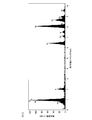
- a precipitate having a particle diameter of 1 to 10 nm was observed at a magnification of 750,000 (observation visual field area was about 2 ⁇ 10 4 nm 2 ) (FIG. 3).
- electron diffraction on a precipitate having a particle size of about 20 nm confirmed that the precipitate is a hexagonal or Fe 2 P orthorhombic crystal having a Fe 2 P-based or Ni 2 P-based crystal structure. It was done.
- the precipitate subjected to electron diffraction is a black oval portion in the center of FIG.
- the result of having analyzed the composition of the deposit using EDX energy dispersive X-ray spectroscopy) is shown in FIG. From FIG. 5, it was confirmed that the precipitate contains Ni, Fe, and P, that is, a kind of [Ni, Fe] -P-based precipitate that has already been defined.
- volume fraction of precipitates The volume fraction of the precipitate was calculated as follows. First, an equivalent circle diameter corresponding to a precipitate having a particle size of 10 to 100 nm in the observation field of 150,000 times shown in FIG. 2 is obtained by image processing, and the size of each precipitate is calculated from the obtained diameter. And the volume was calculated. Next, an equivalent circle diameter corresponding to a precipitate having a particle size of 1 to 10 nm in an observation field of view of 750,000 times shown in FIG. 3 is obtained by image processing, and each precipitate is calculated from the obtained diameter. Size and volume were calculated. The sum of the volume fractions of both was taken as the volume fraction of the precipitate having a particle size of 1 to 100 nm.
- the sample film thickness was measured using the contamination method.
- contamination was attached to a part of the sample, and the sample thickness t was determined from the increase ⁇ L in the length of the contamination when the sample was tilted by ⁇ using the following equation.
- t ⁇ L / sin ⁇
- the volume fraction of precipitates with a particle size of 10 to 100 nm was 0.07%
- the precipitate with a particle size of 1 to 10 nm The volume fraction (precipitate volume fraction by observation at a magnification of ⁇ 750,000) was 0.05%.
- the total volume fraction of the precipitates containing Fe, Ni, and P having a particle diameter of 1 to 100 nm and having precipitates having an Fe 2 P-based or Ni 2 P-based crystal structure is 0.12 in total. %, which was within the range of the desired volume fraction (0.001 to 1.0%) in the present invention. No. of other examples of the present invention. 4, no. 13, no. 17, no. Similarly, the volume fraction of the precipitate was also measured for No. 18, but as shown in Table 13, all were within the range of the desirable volume fraction in the present invention.
- CI value After mechanical polishing is performed on a surface perpendicular to the rolling direction of the strip for property evaluation, that is, a TD (Transverse direction) surface using water-resistant abrasive paper and diamond abrasive grains, a colloidal silica solution is used. Final polishing was performed. And an EBSD measuring device (Quanta FEG 450 made by FEI, EDAX / TSL (current AMETEK) OIM Data Collection) and analysis software (EDAX / TSL (current AMETEK) OIM Data Analysis ver. 5.3).
- the orientation difference of each crystal grain is analyzed in the measurement area of 1000 ⁇ m 2 or more at an acceleration voltage of 20 kV and a measurement interval of 0.1 ⁇ m, and the reliability index (CI value) value of each measurement point is calculated. Calculated. Thereafter, a ratio of CI values of 0.1 or less with respect to all measurement points was calculated. For the measurement, a visual field with a non-unique structure was selected for each strip, 10 visual fields were measured, and the average value was used as a value. Thereafter, the CI value was actually measured in addition to the above-mentioned [crystal grain size observation].
- Tables 9 to 12 show the results of the observation of each structure and the evaluation results.
- No. Nos. 1 to 17 are examples of the present invention based on a Cu-30Zn alloy containing about 30% Zn
- No. No. 18 is an example of the present invention based on a Cu-25Zn alloy containing about 25% Zn
- No. 18 No. 19 is an example of the present invention based on a Cu-20Zn alloy containing about 20% Zn
- Nos. 20 to 28 are examples of the present invention based on a Cu-15Zn alloy containing about 15% Zn
- No. No. 29 is an example of the present invention based on a Cu-10Zn alloy containing about 10% Zn, No. 29. Nos.
- 30 to 38 are examples of the present invention based on a Cu-5Zn alloy containing about 5% of Zn
- No. No. 39 is an example of the present invention based on a Cu-3Zn alloy containing about 3% Zn
- No. 40 is an example of the present invention based on a Cu-30Zn alloy containing about 30% Zn
- No. 41 is an example of the present invention based on a Cu-20-25Zn alloy containing 20-25% Zn.
- No. 42 is an example of the present invention based on a Cu-15Zn alloy containing about 15% Zn
- Nos. 43 to 45 are examples of the present invention based on a Cu-5 to 10Zn alloy containing 5 to 10% Zn.
- No. 46 is an example of the present invention based on a Cu-3Zn alloy containing about 3% Zn.
- No. 47 is an example of the present invention based on a Cu-20-25Zn alloy containing 20-25% Zn, No. 47.
- No. 48 is an example of the present invention based on a Cu-15Zn alloy containing about 15% Zn, No. 48.
- No. 49 is an example of the present invention based on a Cu-5-10Zn alloy containing 5-10% Zn.
- No. 50 is an example of the present invention based on a Cu-3Zn alloy containing about 3% Zn.
- Nos. 51 to 54 are examples of the present invention based on a Cu-5Zn alloy.
- 55 to 58 are examples of the present invention based on a Cu-10Zn alloy.
- No. No. 101 is a comparative example in which the average grain size exceeded the upper limit of the range of the present invention for an alloy based on a Cu-30Zn alloy containing about 30% Zn.
- Nos. 102 to 105 are comparative examples based on a Cu-30Zn alloy containing about 30% Zn
- No. Nos. 106 to 111 are comparative examples based on a Cu-15Zn alloy containing about 15% Zn
- Nos. 112 to 117 are comparative examples based on a Cu-5Zn alloy containing about 5% Zn
- 118 is a comparative example based on a Cu-3Zn alloy containing about 3% Zn.
- the comparative example No. Nos. 101 to 118 were inferior to the examples of the present invention in at least one of stress relaxation resistance and strength (proof strength).
- No. of the comparative example. No. 101 was inferior in yield strength because the average crystal grain size was coarser than 50 ⁇ m.
- the comparative example No. No. 102 is a Cu-30Zn alloy to which Sn, Ni, Fe, and P are not added. In this case, not only the proof stress is lower than the Cu-30Zn-based alloy of the present invention, but also the stress relaxation resistance is inferior. It was.
- Comparative Example No. 103 is a Cu-30Zn-based alloy to which Ni is not added, and not only the Fe / Ni ratio but also the (Ni + Fe) / P ratio and Sn / (Ni + Fe) are outside the scope of the present invention. The stress relaxation resistance was inferior. Comparative Example No.
- Comparative Example No. No. 105 is a Cu-30Zn base alloy to which no Fe was added, and the Fe / Ni ratio was outside the range of the present invention, and in this case, the proof stress was lower than that of the Cu-30Zn base alloy of the present invention example. .
- Comparative Example No. 106 is a Cu-15Zn alloy to which Sn, Ni, Fe, and P are not added. In this case, not only the proof stress is lower than the Cu-15Zn-based alloy of the present invention but also the stress relaxation resistance is inferior. It was. Comparative Example No. No. 107 is a Cu-15Zn alloy to which Ni, Fe, and P are not added. In this case, not only the proof stress is lower than the Cu-15Zn-based alloy of the present invention example, but also the stress relaxation resistance is inferior. . Comparative Example No. No. 108 is a Cu-15Zn-based alloy to which Ni and Fe are not added.
- Comparative Example No. 109 is a Cu-15Zn-based alloy to which Ni is not added, and not only the Fe / Ni ratio but also the (Ni + Fe) / P ratio and Sn / (Ni + Fe) are outside the scope of the present invention.
- the stress relaxation resistance was inferior.
- Comparative Example No. 110 is a Cu-15Zn-based alloy having an Fe / Ni ratio exceeding the range of the present invention, and in this case, the stress relaxation resistance was inferior.
- Comparative Example No. 111 is a Cu-15Zn-based alloy to which no Fe was added, and in this case, the proof stress was lower than that of the Cu-15Zn-based alloy of the example of the present invention.
- Comparative Example No. No. 112 is a Cu-5Zn alloy to which Sn, Ni, Fe, and P are not added. In this case, not only the proof stress is lower than the Cu-5Zn-based alloy of the present invention but also the stress relaxation resistance is inferior. It was. Comparative Example No. No. 113 is a Cu-5Zn-based alloy to which Ni, Fe, and P are not added, and comparative example No. 113. 114 is a Cu-5Zn-based alloy to which Ni and Fe are not added. In these cases, not only the proof stress is lower than the Cu-5Zn-based alloy of the present invention example, but also the stress relaxation resistance is inferior. It was. Comparative Example No.
- Comparative Example No. 115 is a Cu-5Zn based alloy to which Ni is not added, and not only the Fe / Ni ratio but also the (Ni + Fe) / P ratio is outside the scope of the present invention, and in this case, the stress relaxation resistance is inferior. It was. Comparative Example No. 116 is a Cu-5Zn based alloy having an Fe / Ni ratio exceeding the range of the present invention, and in this case, the stress relaxation resistance was inferior. Comparative Example No. 117 is an alloy based on Cu-5Zn without addition of Fe, and not only the Fe / Ni ratio but also the (Ni + Fe) / P ratio is outside the scope of the present invention. In this case, the Cu-5Zn of the present invention example The yield strength was lower than that of the base alloy.
- Reference numeral 118 denotes a Cu-3Zn alloy to which Sn, Ni, Fe, and P are not added. In this case, not only the proof stress is lower than the Cu-3Zn-based alloy of the present invention but also the stress relaxation resistance is inferior. It was.
- a Cu—Zn—Sn based copper alloy having high strength and excellent characteristics such as bending workability and conductivity, and a copper alloy member such as a thin plate made of such a copper alloy are provided. be able to.
- Such a copper alloy can be suitably used for electronic and electrical equipment parts such as connectors and other terminals, movable conductive pieces of electromagnetic relays, and lead frames.
Landscapes
- Chemical & Material Sciences (AREA)
- Engineering & Computer Science (AREA)
- Mechanical Engineering (AREA)
- Organic Chemistry (AREA)
- Metallurgy (AREA)
- Materials Engineering (AREA)
- Crystallography & Structural Chemistry (AREA)
- Physics & Mathematics (AREA)
- Thermal Sciences (AREA)
- Manufacturing & Machinery (AREA)
- Conductive Materials (AREA)
- Non-Insulated Conductors (AREA)
- Metal Rolling (AREA)
- Powder Metallurgy (AREA)
Abstract
Description
本願は、2012年1月6日に、日本に出願された特願2012-001177号および2012年9月14日に、日本に出願された特願2012-203517号に基づき優先権を主張し、その内容をここに援用する。
上述のようにCu-Zn合金を基材としてその表面にSnめっきを施したコネクタなどの導電部品においては、Snめっき材のリサイクル性を向上させるとともに、強度を向上させるため、基材のCu-Zn合金自体についても、合金成分としてSnを添加したCu-Zn―Sn系合金を使用する場合がある。
これらの特許文献1、2の提案に示されるように、Cu-Zn―Sn系合金にNi、Fe、Pを添加することが耐応力緩和特性の向上に有効であること自体は、本発明者等も確認しているが、特許文献1、2の提案ではNi、Fe、Pの個別の含有量が考慮されているだけである。このような個別の含有量の調整だけでは、必ずしも耐応力緩和特性を確実かつ十分に向上させることができないことが、本発明者等の実験、研究によって判明している。
このような特許文献3の提案に示されているNi/Sn比の調整も、確かに耐応力緩和特性の向上に有効ではあるが、P化合物と耐応力緩和特性との関係についてはまったく触れられていない。すなわちP化合物は、特許文献1、2に示されているように耐応力緩和特性に大きな影響を及ぼすと思われるが、特許文献3の提案では、P化合物を生成するFe、Niなどの元素に関しては、その含有量と耐応力緩和特性との関係が全く考慮されておらず、本発明者等の実験でも、特許文献3の提案に従っただけでは、十分かつ確実な耐応力緩和特性の向上を図りが得られないことが判明している。
しかしながら、本発明者等の実験によれば、特許文献4で規定されているようにFe、Ni、Pの合計量と、(Fe+Ni)/Pの原子比とを調整しただけでは、耐応力緩和特性の十分な向上は図り得られないことが判明した。その理由は定かではないが、耐応力緩和特性の確実かつ十分な向上のためには、Fe、Ni、Pの合計量と(Fe+Ni)/Pの調整以外に、Fe/Ni比の調整、さらにはSn/(Ni+Fe)の調整が重要であって、これらの各含有量比率をバランス良く調整しなければ、耐応力緩和特性を確実かつ十分な向上させ得ないことが、本発明者等の実験、研究によって判明している。
またさらに、上記のNi、Fe、Pと同時に適量のCoを添加することにより、耐応力緩和特性および強度をより一層向上させることができることを見い出した。
かつFeの含有量とNiの含有量との比Fe/Niが、原子比で、0.002≦Fe/Ni<1.5を満たし、
NiおよびFeの合計含有量(Ni+Fe)とPの含有量との比(Ni+Fe)/Pが、原子比で、3<(Ni+Fe)/P<15を満たし、
Snの含有量とNiおよびFeの合計量(Ni+Fe)との比Sn/(Ni+Fe)が、原子比で、0.3<Sn/(Ni+Fe)<5を満たすように定められ、
Cu、ZnおよびSnを含有するα相の結晶粒の平均粒径が0.1~50μmの範囲内にあり、さらにFeおよび/またはNiとPとを含有する析出物が含まれていることを特徴としている銅合金である。
質量%で、Znを2.0%を越え、36.5%以下、Snを0.1%以上、0.9%以下、Niを0.05%以上、1.0%未満、Feを0.001%以上、0.10%未満、Coを0.001%以上、0.10%未満、Pを0.005%以上、0.10%以下含有し、残部がCuおよび不可避的不純物よりなり、
かつFeおよびCoの合計含有量とNiの含有量との比(Fe+Co)/Niが、原子比で、0.002≦(Fe+Co)/Ni<1.5を満たし、
Ni、FeおよびCoの合計含有量(Ni+Fe+Co)とPの含有量との比(Ni+Fe+Co)/Pが、原子比で、3<(Ni+Fe+Co)/P<15を満たし、
Snの含有量とNi、FeおよびCoの合計含有量(Ni+Fe+Co)との比Sn/(Ni+Fe+Co)が、原子比で、0.3<Sn/(Ni+Fe+Co)<5を満たすように定められ、
Cu、ZnおよびSnを含有する相(α相)からなる結晶粒の平均粒径が0.1~50μmの範囲内にあり、FeとNiとCoから選択される一種以上の元素とPとを含有する析出物が含まれていることを特徴としている銅合金である。
さらに第6~第8の態様は、第5の態様で規定する、Coを含有する系の合金について、前記第2~第4の態様に準じて、析出物などの組織を規定している。
上記第1から第9の態様にかかる銅合金、また前記第10の態様にかかる電子・電気機器用銅合金薄板では、α相について、EBSD法により1000μm2以上の測定面積を測定間隔0.1μmステップで測定して、データ解析ソフトOIMにより解析したときのCI値が0.1以下である測定点の割合が、70%以下であってもよい。
質量%で、Znを2.0%を越え、36.5%以下、Snを0.1%以上、0.9%以下、Niを0.05%以上、1.0%未満、Feを0.001%以上、0.10%未満、Pを0.005%以上、0.10%以下含有し、残部がCuおよび不可避的不純物よりなり、
かつFeの含有量とNiの含有量との比Fe/Niが、原子比で、0.002≦Fe/Ni<1.5を満たし、
NiおよびFeの合計含有量(Ni+Fe)とPの含有量との比(Ni+Fe)/Pが、原子比で、3<(Ni+Fe)/P<15を満たし、
Snの含有量とNiおよびFeの合計量(Ni+Fe)との比Sn/(Ni+Fe)が、原子比で、0.3<Sn/(Ni+Fe)<5を満たすように定められた合金を素材とし、
前記素材に少なくとも1回の塑性加工(後述する実施形態における中間塑性加工に相当)と、再結晶及び析出のための少なくとも1回の熱処理(後述する実施形態における中間熱処理工程に相当)とを含む工程を施して、再結晶組織を有する所定の板厚の再結晶板に仕上げ、さらにその再結晶板に対して加工率1~70%の仕上げ塑性加工を施し、
これによって、Cu、ZnおよびSnを含有するα相の結晶粒の平均粒径が0.1~50μmの範囲内にあり、しかもEBSD法により1000μm2以上の測定面積を測定間隔0.1μmステップで測定して、データ解析ソフトOIMにより解析したときのCI値が0.1以下である測定点の割合が、70%以下である銅合金を得ることを特徴としている製造方法である。
質量%で、Znを2.0%を越え、36.5%以下、Snを0.1%以上、0.9%以下、Niを0.05%以上、1.0%未満、Feを0.001%以上、0.10%未満、Coを0.001%以上、0.10%未満、Pを0.005%以上、0.10%以下含有し、残部がCuおよび不可避的不純物よりなり、
かつFeおよびCoの合計含有量とNiの含有量との比(Fe+Co)/Niが、原子比で、0.002≦(Fe+Co)/Ni<1.5を満たし、
Ni、FeおよびCoの合計含有量(Ni+Fe+Co)とPの含有量との比(Ni+Fe+Co)/Pが、原子比で、3<(Ni+Fe+Co)/P<15を満たし、
Snの含有量とNi、FeおよびCoの合計含有量(Ni+Fe+Co)との比Sn/(Ni+Fe+Co)が、原子比で、0.3<Sn/(Ni+Fe+Co)<5を満たすように定められた合金を素材とし、
前記素材に少なくとも1回の塑性加工(後述する実施形態における中間塑性加工に相当)と、再結晶及び析出のための少なくとも一回の熱処理(後述する実施形態における中間熱処理工程に相当)とを含む工程を施して、再結晶組織を有する所定の板厚の再結晶板に仕上げ、
前記再結晶板に対して加工率1~70%の仕上げ塑性加工を施し、
これによって、Cu、ZnおよびSnを含有するα相の結晶粒の平均粒径が0.1~50μmの範囲内にあり、しかもEBSD法により1000μm2以上の測定面積を測定間隔0.1μmステップで測定して、データ解析ソフトOIMにより解析したときのCI値が0.1以下である測定点の割合が、70%以下である銅合金を得ることを特徴としている製造方法である。
ここで、EBSDにより測定してOIMにより解析した測定点の組織が加工組織である場合、結晶パターンが明確ではないため結晶方位決定の信頼性が低くなり、その場合にCI値が低くなる。特にCI値が0.1以下の場合にその測定点の組織が加工組織であると判断することができる。そしてCI値0.1以下の加工組織と判断される測定点が、1000μm2以上の測定面積内で70%以下であれば、実質的に再結晶組織が維持されていると判断でき、その場合には加工組織によって曲げ加工性を損なってしまうことを有効に防止できる。
このように仕上げ塑性加工の後、さらに、50~800℃において0.1秒~24時間加熱する低温焼鈍を施せば、耐応力緩和特性を向上させ、材料内部に残留する歪によって、材料に反りなどの変形が生じてしまうことを防止することができる。
また、本発明の第16の態様による端子は、前記第1~第9の態様の電子・電気機器用銅合金からなる端子である。
本発明の第17の態様による電子・電気機器用導電部品は、前記第10または第11の態様の電子・電気機器用銅合金薄板からなり、曲げ部分のバネ性により相手側導電部材に圧接させ、相手側導電部材との電気的導通を確保することを特徴としている導電部品である。
また、本発明の第18の態様による端子は、前記第10または第11の態様の電子・電気機器用銅合金薄板からなる端子である。
本発明の電子・電気機器用銅合金は、基本的には、合金元素の個別の含有量としては、質量%で、Znを2.0%を越え、36.5%以下、Snを0.1以上、0.9%以下、Niを0.05%以上、1.0%未満、Feを0.001%以上、0.10%未満、Pを0.005%以上、0.10%以下含有するものであり、さらに各合金元素の相互間の含有量比率として、Feの含有量とNiの含有量との比Fe/Niが、原子比で、次の(1)式
0.002≦Fe/Ni<1.5 ・・・(1)
を満たし、かつNiの含有量およびFeの含有量の合計量(Ni+Fe)とPの含有量との比(Ni+Fe)/Pが、原子比で、次の(2)式
3<(Ni+Fe)/P<15 ・・・(2)
を満たし、さらにSnの含有量とNiの含有量およびFeの含有量の合計量(Ni+Fe)との比Sn/(Ni+Fe)が、原子比で、次の(3)式
0.3<Sn/(Ni+Fe)<5 ・・・(3)
を満たすように定められ、上記各合金元素の残部がCuおよび不可避的不純物とされ、さらに組織条件として、Cu、ZnおよびSnを含有するα相の結晶粒の平均粒径が0.5~50μmの範囲内にあり、しかもFeおよび/またはNiとPとを含有する析出物が含まれているものである。なお以下では、上記の析出物について、〔Ni,Fe〕-P系析出物というものとする。
0.002≦(Fe+Co)/Ni<1.5 ・・・(1´)
を満たし、さらにNi、FeおよびCoの合計含有量(Ni+Fe+Co)とPの含有量との比(Ni+Fe+Co)/Pが、原子比で、次の(2´)式
3<(Ni+Fe+Co)/P<15 ・・・(2´)
を満たし、さらにSnの含有量とNi、FeおよびCoの合計含有量(Ni+Fe+Co)との比Sn/(Ni+Fe+Co)が、原子比で、次の(3´)式
0.3<Sn/(Ni+Fe+Co)<5 ・・・(3´)
を満たすように定められ、上記各合金元素の残部がCuおよび不可避的不純物とされ、さらに組織条件として、上記と同様な条件を満たすものである。なお以下では、この場合の析出物を、〔Ni,Fe,Co〕-P系析出物と称する。
本発明の一形態にかかる電子・電気機器用銅合金は、質量%で、Znを2.0%を越え、36.5%以下、Snを0.1~0.9%、Niを0.05%以上、1.0%未満、Pを0.005~0.10%、Feを0.001%以上、0.10%未満、Coを0.10%未満含有し、残部がCuおよび不可避的不純物からなり、
FeとNiの含有量の比Fe/Niが、原子比で、0.002≦Fe/Niを満たし、
FeおよびCoの合計含有量とNiの含有量の比(Fe+Co)/Niが、原子比で、(Fe+Co)/Ni<1.5を満たし、
NiおよびFeの合計含有量(Ni+Fe)とPの含有量との比(Ni+Fe)/Pが、原子比で、3<(Ni+Fe)/Pを満たし、
Ni、FeおよびCoの合計含有量(Ni+Fe+Co)とPの含有量との比(Ni+Fe+Co)/Pが、原子比で、(Ni+Fe+Co)/P<15を満たし、
Snの含有量とNiおよびFeの合計量(Ni+Fe)との比Sn/(Ni+Fe)が、原子比で、Sn/(Ni+Fe)<5を満たし、
Snの含有量とNi、FeおよびCoの合計含有量(Ni+Fe+Co)との比Sn/(Ni+Fe+Co)が、原子比で、0.3<Sn/(Ni+Fe+Co)を満たすように定められ、
Cu、ZnおよびSnを含有するα相の結晶粒の平均粒径が0.5~50μmの範囲内にあり、Fe、Ni、Coから選択される一種以上およびPを含有する析出物が含まれている銅合金である。
亜鉛(Zn):質量%で、2.0%を越え、36.5%以下
Znは、本発明で対象としている銅合金(黄銅)において基本的な合金元素であり、強度およびばね性の向上に有効な元素である。またZnはCuより安価であるため、銅合金の材料コストの低減にも効果がある。Znが2.0%以下では、材料コストの低減効果が十分に得られない。一方Znが36.5%を越えれば、銅合金の耐応力緩和特性が低下してしまい、後述するように本発明に従ってFe、Ni、Pを添加しても、十分な耐応力緩和特性を確保することが困難となる。また銅合金の耐食性が低下するとともに、β相が多量に生じるため冷間圧延性および曲げ加工性も低下してしまう。したがってZnの含有量は2.0%を越え、36.5%以下の範囲内とした。なおZn量は、上記の範囲内でも4.0~36.5%の範囲内が好ましく、更には8.0~32.0%の範囲内が好ましく、特に8.0~27.0%の範囲内が好ましい。
Snの添加は強度向上に効果があり、またSnめっきを施して使用する電子・電気機器材料の母材黄銅合金として、Snを添加しておくことが、Snめっき付き黄銅材のリサイクル性の向上に有利となる。さらにSnがNiおよびFeと共存すれば、銅合金の耐応力緩和特性の向上にも寄与することが本発明者等の研究により判明している。Snが0.1%未満ではこれらの効果が十分に得られず、一方Snが0.9%を越えれば、銅合金の熱間加工性および冷間圧延性が低下してしまい、熱間圧延や冷間圧延で割れが発生してしまうおそれがあり、また導電率も低下してしまう。そこでSnの添加量は0.1%以上、0.9%以下の範囲内とした。
なおSn量は、上記の範囲内でも特に0.2%以上、0.8%以下の範囲内が好ましい。
Niは、Fe、Pと並んで本発明において特徴的な添加元素であり、Cu-Zn―Sn合金に適量のNiを添加して、NiをFe、Pと共存させることによって、〔Ni,Fe〕-P系析出物を母相(α相主体)から析出させることができ、また、NiをFe、Co、Pと共存させることによって、〔Ni,Fe,Co〕-P系析出物を母相(α相主体)から析出させることができる。これらの〔Ni,Fe〕-P系析出物もしくは〔Ni,Fe,Co〕-P系析出物が存在することによって、再結晶の際に結晶粒界をピン止めする効果により、母相の平均結晶粒径を小さくすることができ、その結果、強度を増加させることができる。またこのように母相の平均結晶粒径を小さくすることによって、曲げ加工性や耐応力腐食割れ性も向上させることができる。さらに、これらの析出物の存在により、耐応力緩和特性を大幅に向上させることができる。加えて、NiをSn、Fe、Co、Pと共存させることで析出物による耐応力緩和特性の向上だけでなく、固溶強化によっても向上させることができる。ここで、Niの添加量が0.05%未満では、耐応力緩和特性を十分に向上させることができない。一方Niの添加量が1.0%以上となれば、銅合金に固溶Niが多くなって導電率が低下し、また高価なNi原材料の使用量の増大によりコスト上昇を招く。そこでNiの添加量は0.05%以上、1.0%未満の範囲内とした。なおNiの添加量は、上記の範囲内でも特に0.05%以上、0.8%未満の範囲内とすることが好ましい。
Feは、Ni、Pと並んで本発明において特徴的な添加元素であり、Cu-Zn―Sn合金に適量のFeを添加して、FeをNi、Pと共存させることによって、〔Ni,Fe〕-P系析出物を母相(α相主体)から析出させることができ、また、FeをNi、Co、Pと共存させることによって、〔Ni,Fe,Co〕-P系析出物を母相(α相主体)から析出させることができる。これらの〔Ni,Fe〕-P系析出物もしくは〔Ni,Fe,Co〕-P系析出物が存在することによって、母相の再結晶の際に結晶粒界をピン止めする効果により、母相の平均粒径を小さくすることができ、その結果、強度を増加させることができる。またこのように平均結晶粒径を小さくすることによって、曲げ加工性や耐応力腐食割れ性も向上させることができる。さらに、これらの析出物の存在により、銅合金の耐応力緩和特性を大幅に向上させることができる。ここで、Feの添加量が0.001%未満では、結晶粒界をピン止めする効果が充分に得られず、そのため充分な強度が得られない。一方Feの添加量が0.10%以上となれば、銅合金に一層の強度向上は認められず、固溶Feが多くなって導電率が低下し、また冷間圧延性も低下してしまう。そこでFeの添加量は0.001%以上、0.10%未満の範囲内とした。なおFeの添加量は、上記の範囲内でも特に0.005%以上、0.08%以下の範囲内とすることが好ましい。
Coは、必ずしも必須の添加元素ではないが、少量のCoをNi、Fe、Pとともに添加すれば、〔Ni,Fe,Co〕-P系析出物が生成され、銅合金の耐応力緩和特性をより一層向上させることができる。ここでCo添加量が0.001%未満では、Co添加による耐応力緩和特性のより一層の向上効果が得られず、一方Co添加量が0.10%以上となれば、固溶Coが多くなって銅合金の導電率が低下し、また高価なCo原材料の使用量の増大によりコスト上昇を招く。そこでCoを添加する場合のCoの添加量は0.001%以上、0.10%未満の範囲内とした。なおCoの添加量は、上記の範囲内でも特に0.005%以上、0.08%以下の範囲内とすることが好ましい。なおCoを積極的に添加しない場合でも、不純物として0.001%未満のCoが含有されることがある。
Pは、Fe、Ni、さらにはCoとの結合性が高く、Fe、Niとともに適量のPを含有させれば、〔Ni,Fe〕-P系析出物を析出させることができ、またFe、Ni、Coとともに適量のPを含有させれば、〔Ni,Fe,Co〕-P系析出物を析出させることができる。そしてこれらの析出物の存在によって耐応力緩和特性を向上させることができる。ここで、P量が0.005%未満では、十分に〔Ni,Fe〕-P系析出物または〔Ni,Fe,Co〕-P系析出物を析出させることが困難となり、十分に銅合金の耐応力緩和特性を向上させることができなくなる。一方P量が0.10%を越えれば、P固溶量が多くなって、導電率が低下するとともに圧延性が低下して冷間圧延割れが生じやすくなってしまう。そこでPの含有量は、0.005%以上、0.10%以下の範囲内とした、なおP量は、上記の範囲内でも特に0.01%以上、0.08%以下の範囲内が好ましい。
なおまた、Pは、銅合金の溶解原料から不可避的に混入することが多い元素であり、従ってP量を上述のように規制するためには、溶解原料を適切に選定することが望ましい。
本発明者等の詳細な実験によれば、耐応力緩和特性にはFe/Ni比が大きな影響を与え、その比が特定の範囲内にある場合に、はじめて耐応力緩和特性を十分に向上させ得ることが判明した。すなわち、FeとNiを共存させ、かつFe、Niのそれぞれの含有量を前述のように調整するだけではなく、それらの比Fe/Niを、原子比で、0.002以上かつ1.5未満の範囲内とした場合に、十分な耐応力緩和特性の向上が得られることを見い出した。ここで、Fe/Ni比が1.5以上となれば、耐応力緩和特性が低下し、またFe/Ni比が0.002未満であれば強度が低下する。また、Fe/Ni比が0.002未満では、高価なNiの原材料使用量が相対的に多くなって、コスト上昇を招く。そこでFe/Ni比は、上記の範囲内に規制することとした。なおFe/Ni比は、上記の範囲内でも、特に0.005以上1以下の範囲内が望ましい。さらに望ましくは0.005以上0.5以下の範囲内が好ましい。
NiおよびFeがPと共存することにより、〔Ni,Fe〕-P系析出物が生成されて、その〔Ni,Fe〕-P系析出物の分散により耐応力緩和特性を向上させることができるが。他方、(Ni+Fe)に対してPが過剰に含有されれば、固溶Pの割合の増大によって逆に耐応力緩和特性が低下してしまい、またPに対して(Ni+Fe)が過剰に含有されれば、固溶したNi、Feの割合の増大によって耐応力緩和特性が低下してしまう。そこで、耐応力緩和特性の十分な向上のためには、(Ni+Fe)/P比の制御も重要である。(Ni+Fe)/P比が3以下では、固溶Pの割合の増大に伴って銅合金の耐応力緩和特性が低下し、また同時に固溶Pにより銅合金の導電率が低下するとともに、圧延性が低下して冷間圧延割れが生じやすくなり、さらに曲げ加工性も低下する。一方、(Ni+Fe)/P比が15以上となれば、固溶したNi、Feの割合の増大により銅合金の導電率が低下してしまう。そこで(Ni+Fe)/P比を上記の範囲内に規制することとした。なお(Ni+Fe)/P比は、上記の範囲内でも、特に3を越え、12以下の範囲内が望ましい。
前述のようにSnがNiおよびFeと共存すれば、Snは耐応力緩和特性の向上に寄与するが、その耐応力緩和特性向上効果は、Sn/(Ni+Fe)比が特定の範囲内でなければ十分に発揮されない。すなわち、Sn/(Ni+Fe)比が0.3以下では、十分な耐応力緩和特性向上効果が発揮されず、一方Sn/(Ni+Fe)比が5以上となれば、相対的に(Ni+Fe)量が少なくなって、〔Ni,Fe〕-P系析出物の量が少なくなり、耐応力緩和特性が低下してしまう。なおSn/(Ni+Fe)比は、上記の範囲内でも、特に0.3を超え、2.5以下の範囲内が望ましい。さらに好ましくは、0.3を超え、1.5以下の範囲内が望ましい。
Coを添加した場合、Feの一部をCoで置き換えたと考えればよい。したがって(1´)式も基本的には(1)式に準じている。すなわち、Fe、Niに加えてCoを添加した場合、耐応力緩和特性には(Fe+Co)/Ni比が大きな影響を与え、その比が特定の範囲内にある場合に、はじめて耐応力緩和特性を十分に向上させ得る。したがって、NiとFeおよびCoを共存させ、かつFe、Ni、Coのそれぞれの含有量を前述のように調整するだけではなく、FeとCoの合計含有量とNi含有量との比(Fe+Co)/Niを、原子比で、0.002以上かつ1.5未満の範囲内とした場合に、十分な耐応力緩和特性の向上を図り得ることを見い出した。ここで、(Fe+Co)/Ni比が1.5以上となれば、耐応力緩和特性が低下し、また(Fe+Co)/Ni比が0.002未満であれば強度が低下する。また、(Fe+Co)/Ni比が0.002未満では、高価なNiの原材料使用量が相対的に多くなって、コスト上昇を招く。そこで(Fe+Co)/Ni比は、上記の範囲内に規制することとした。なお(Fe+Co)/Ni比は、上記の範囲内でも、特に0.005以上1以下の範囲内が望ましい。さらに望ましくは0.005以上0.5以下の範囲内が好ましい。
Coを添加する場合の(2´)式も、前記(2)式に準じている。すなわち、Ni、FeおよびCoがPと共存することにより、〔Ni,Fe,Co〕-P系析出物が生成されて、その〔Ni,Fe,Co〕-P系析出物の分散により耐応力緩和特性を向上させることができる。しかし、(Ni+Fe+Co)に対してPが過剰に含有されれば、固溶Pの割合の増大によって逆に耐応力緩和特性が低下してしまう。したがって、耐応力緩和特性の十分な向上のためには、(Ni+Fe+Co)/P比も重要である。(Ni+Fe+Co)/P比が3以下では、固溶Pの割合の増大に伴って銅合金の耐応力緩和特性が低下し、また同時に固溶Pにより銅合金の導電率が低下するとともに、圧延性が低下して冷間圧延割れが生じやすくなり、さらに曲げ加工性も低下する。一方、(Ni+Fe+Co)/P比が15以上となれば、固溶したNi、Fe、Coの割合の増大により導電率が低下してしまう。そこで(Ni+Fe+Co)/P比を上記の範囲内に規制することとした。なお(Ni+Fe+Co)/P比は、上記の範囲内でも、特に3を越え、12以下の範囲内が望ましい。
Coを添加する場合の(3´)式も、前記(3)式に準じている。すなわち、SnがNi、FeおよびCoと共存すれば、Snは耐応力緩和特性の向上に寄与するが、その耐応力緩和特性向上効果は、Sn/(Ni+Fe+Co)比が特定の範囲内でなければ十分に発揮されない。具体的には、Sn/(Ni+Fe+Co)比が0.3以下では、十分な耐応力緩和特性向上効果が発揮されず、一方Sn/(Ni+Fe+Co)比が5以上となれば、相対的に(Ni+Fe+Co)量が少なくなって、〔Ni,Fe,Co〕-P系析出物の量が少なくなり、耐応力緩和特性が低下してしまう。なおSn/(Ni+Fe+Co)比は、上記の範囲内でも、特に0.3を超え、2.5以下の範囲内が望ましい。さらに好ましくは、0.3を超え、1.5以下の範囲内が望ましい。
さらに本発明の電子・電気機器用銅合金中における平均粒径100nm以下の微細な析出物の割合は、体積分率で0.001%以上、1%以下の範囲内であることが望ましい。平均粒径100nm以下の微細な析出物の体積分率が0.001%未満では、銅合金において、良好な耐応力緩和特性を確保することが困難となり、また強度と曲げ加工性を向上させる効果も充分に得られなくなる。一方、その体積分率が1%を越えれば、銅合金の曲げ加工性が低下する。なお平均粒径100nm以下の微細な析出物の割合は、体積分率で0.005%~0.5%の範囲内、さらに0.01%~0.2%の範囲内であることが、より望ましい。
すなわち、銅合金の製品としての耐力を向上させるための処理としては、後に改めて製造方法の説明で述べるように、最終的に仕上げ塑性加工を行うことが望ましい。これは銅合金の製品としての耐力を向上させるための処理であり、その加工方法は特に限定されないが、最終形態が板や条である場合、圧延を適用するのが通常である。そして圧延により仕上げ塑性加工を行なった場合、結晶粒が圧延方向に対して平行な方向に伸長するように変形する。
一方、EBSD装置の解析ソフトOIMにより解析したときのCI値(信頼性指数)は、測定点の結晶パターンが明確ではない場合にその値が小さくなり、CI値が0.1以下では加工組織となっているとみなすことができる。そして、CI値が0.1以下の測定点の割合が70%以下である場合は、実質的に再結晶組織が維持されて、曲げ加工性が損なわれないのである。
なおEBSD法による測定面は、仕上げ塑性加工を圧延によって行った場合には、圧延幅方向に対し垂直な面(縦断面)、すなわちTD(Transverse Direction)面とする。仕上げ塑性加工を圧延以外の方法によって行った場合は、圧延の場合のTD面に準じて、主加工方向に沿った縦断面を測定面とすればよい。
本発明の銅合金からなる部材、例えば、本発明の電子・電気機器用銅合金薄板は、母相(α相)の結晶粒について、上記のCI値により定義される特性を有することができる。
先ず前述のような成分組成の銅合金溶湯を溶製する。ここで、溶解原料のうち銅原料としては、純度が99.99%以上とされたいわゆる4NCu、例えば無酸素銅を使用することが望ましいが、スクラップを原料として用いてもよい。また溶解工程では、大気雰囲気炉を用いてもよいが、Znの酸化を抑制するために、真空炉、あるいは、不活性ガス雰囲気又は還元性雰囲気とされた雰囲気炉を用いてもよい。
次いで成分調整された銅合金溶湯を、適宜の鋳造法、例えば金型鋳造などのバッチ式鋳造法、あるいは連続鋳造法、半連続鋳造法などによって鋳造して、鋳塊(スラブ状鋳塊など)とする。
その後、必要に応じて、鋳塊に対する加熱工程S02として、鋳塊の偏析を解消して鋳塊組織を均一化するために均質化処理を行なう。この均質化処理の条件は特に限定しないが、通常は600~950℃において5分~24時間加熱すればよい。均質化処理温度が600℃未満、あるいは均質化処理時間が5分未満では、十分な均質化効果が得られないおそれがあり、一方均質化処理温度が950℃を越えれば、偏析部位が一部溶解してしまうおそれがあり、さらに均質化処理時間が24時間を越えることはコスト上昇を招くだけである。均質化処理後の冷却条件は、適宜定めれば良いが、通常は水焼入れすればよい。なお均質化処理後には、必要に応じて面削を行なう。
次いで、粗加工の効率化と組織の均一化のために、前述の加熱工程S02の後に、鋳塊に対して熱間加工を行ってもよい。この熱間加工の条件は特に限定されないが、通常は、開始温度600~950℃、終了温度300~850℃、加工率10~99%程度とすることが好ましい。なお熱間加工開始温度までの鋳塊加熱は、前述の加熱工程S02と兼ねて行なってもよい。すなわち均質化処理後に、室温近くまで冷却せずに、熱間加工開始温度まで冷却された状態で熱間加工を開始してもよい。熱間加工後の冷却条件は、適宜定めれば良いが、通常は水焼入れすればよい。なお熱間加工後には、必要に応じて面削を行なう。熱間加工の加工方法については、特に限定されないが、最終形状が板や条の場合は熱間圧延を適用して、0.5~50mm程度の板厚まで圧延すればよい。また最終形状が線や棒の場合には、押出や溝圧延を、また最終形状がバルク形状の場合には、鍛造やプレスを適用すればよい。
前述のように加熱工程S02で均質化処理を施した鋳塊、あるいはさらに必要に応じて熱間圧延などの熱間加工(S03)を施した熱間加工材には、中間塑性加工を施す。この中間塑性加工S04における温度条件は特に限定はないが、冷間又は温間加工となる-200℃から+200℃の範囲内とすることが好ましい。中間塑性加工の加工率も特に限定されないが、通常は10~99%程度とする。加工方法は特に限定されないが、最終形状が板、条の場合は、圧延を適用して板厚0.05~25mm程度の板厚まで冷間もしくは温間で圧延すればよい。また最終形状が線や棒の場合には、押出や溝圧延、さらに最終形状がバルク形状の場合には、鍛造やプレスを適用する事が出来る。なお、溶体化の徹底のために、S02~S04を繰り返しても良い。
冷間もしくは温間での中間塑性加工(S04)、例えば冷間圧延の後には、再結晶処理と析出処理を兼ねた中間熱処理を施す。この中間熱処理は、銅合金の組織を再結晶させると同時に、〔Ni,Fe〕-P系析出物もしくは〔Ni,Fe,Co〕-P系析出物を分散析出させるために重要な工程であり、これらの析出物が生成されるような加熱温度、加熱時間の条件を適用すればよい。中間熱処理の条件は、通常は、200~800℃で、1秒~24時間とすればよい。但し、既に述べたように結晶粒径も耐応力緩和特性にある程度の影響を与えるから、中間熱処理による再結晶粒を測定して、加熱温度、加熱時間の条件を適切に選択することが望ましい。但し、中間熱処理およびその後の冷却は、最終的な平均結晶粒径に影響を与えるから、これらの条件は、α相の平均結晶粒径が0.1~50μmの範囲内となるように選定することが望ましい。
すなわち中間熱処理の具体的手法としては、バッチ式の加熱炉を用いても、あるいは連続焼鈍ラインを用いて連続的に加熱しても良い。そして中間熱処理の好ましい加熱条件は、バッチ式の加熱炉を使用する場合は、300~800℃の温度で、5分~24時間加熱することが望ましく、また連続焼鈍ラインを用いる場合は、加熱到達温度250~800℃とし、かつその範囲内の温度で、保持なし、もしくは1秒~5分程度保持することが好ましい。またこの中間熱処理の雰囲気は、非酸化性雰囲気(窒素ガス雰囲気、不活性ガス雰囲気、あるいは還元性雰囲気)とすることが好ましい。
中間熱処理後の冷却条件は、特に限定しないが、通常は2000℃/秒~100℃/時間程度の冷却速度で冷却すればよい。
中間熱処理工程S05の後には、最終寸法、最終形状まで銅合金の仕上げ加工を行う。仕上げ塑性加工における加工方法は特に限定されないが、銅合金の最終製品形態が板や条である場合には、圧延(冷間圧延)を適用するのが通常であり、その場合は0.05~1.0mm程度の板厚に圧延すればよい。その他、最終製品形態に応じて、鍛造やプレス、溝圧延などを適用しても良い。加工率は最終板厚や最終形状に応じて適宜選択すれば良いが、1~70%の範囲内が好ましい。加工率が1%未満では、耐力を向上させる効果が充分に得られず、一方70%を越えれば、実質的に再結晶組織が失われて、いわゆる加工組織となってしまって、曲げ加工性が低下してしまうという問題が生じる。なお加工率は、好ましくは1~65%、より好ましくは、5~60%とする。ここで、仕上げ塑性加工を圧延によって行なう場合には、その圧延率が加工率に相当する。仕上げ塑性加工後は、これをそのまま製品として、コネクタなどに用いても良いが、通常は、さらに仕上げ熱処理を施すことが好ましい。
仕上げ塑性加工後には、必要に応じて、耐応力緩和特性の向上、及び低温焼鈍硬化のために、又は残留ひずみの除去のために、仕上げ熱処理工程S07を行なう。この仕上げ熱処理は、50~800℃の範囲内の温度で、0.1秒~24時間行なうことが望ましい。
仕上げ熱処理の温度が50℃未満、または仕上げ熱処理の時間が0.1秒未満では、十分な歪み取りの効果が得られなくなるおそれがある。一方仕上げ熱処理の温度が800℃を越える場合は再結晶のおそれがあり、さらに仕上げ熱処理の時間が24時間を越えることは、コスト上昇を招くだけである。なお、仕上げ塑性加工S06を行わない場合には、仕上げ熱処理工程S07は省略してもよい。
具体的には、No.2~4、No.43、No.44、No.46、No.49~58、No.101については、圧延率約90%以上の一次冷間圧延(一次中間塑性加工)を行なった後、再結晶と析出処理のための一次中間熱処理として、200~800℃で、所定時間の熱処理を実施し、水焼入れした。そして一次中間熱処理―水焼入れの後、圧延材を切断するとともに、酸化被膜を除去するために表面研削を実施し、後述する仕上げ塑性加工に供した。
一方、No.1、No.5~42、No.45、No.47、No.48、No.102~118については、圧延率約50~95%の一次冷間圧延(一次中間塑性加工)を行なった後、一次中間熱処理として、200~800℃で、所定時間の熱処理を実施し、水焼入れした後、圧延率約50~95%の二次冷間圧延(二次中間塑性加工)を施し、さらに熱処理後の平均粒径が約10μm以下となるように、200~800℃の間で所定の時間、二次中間熱処理を実施し、水焼入れした。そして二次中間熱処理―水焼入れの後、圧延材を切断するとともに、酸化被膜を除去するために表面研削を実施し、後述する仕上げ塑性加工に供した。
平均粒径が10μmを越える場合については、各試料について圧延面に対して法線方向に垂直な面、すなわちND(Normal Direction)面を観察面とし、鏡面研磨、エッチングを行なってから、光学顕微鏡にて、圧延方向が写真の横になるように撮影し、1000倍の視野(約300×200μm2)で観察を行った。そして、結晶粒径をJIS H 0501の切断法に従い、写真縦、横の所定長さの線分を5本ずつ引き、完全に切られる結晶粒数を数え、その切断長さの平均値を平均結晶粒径として算出した。
また、平均結晶粒径10μm以下の場合は、圧延の幅方向に対して垂直な面、すなわちTD面を観察面として、SEM-EBSD(Electron Backscatter Diffraction Patterns)測定装置によって、平均結晶粒径を測定した。具体的には、耐水研磨紙、ダイヤモンド砥粒を用いて機械研磨を行った後、コロイダルシリカ溶液を用いて仕上げ研磨を行ない、その後、走査型電子顕微鏡を用いて、試料表面の測定範囲内の個々の測定点(ピクセル)に電子線を照射し、後方散乱電子線回折による方位解析により、隣接する測定点間の方位差が15°以上となる測定点間を大角粒界とし、15°以下を小角粒界とした。そして大角粒界を用いて、結晶粒界マップを作成し、JIS H 0501の切断法に準拠し、結晶粒界マップに対して、縦、横の所定長さの線分を5本ずつ引き、完全に切られる結晶粒数を数え、その切断長さの平均値を平均結晶粒径とした。
このようにして調べた一次中間熱処理後の段階、もしくは二次中間熱処理後の段階での平均結晶粒径を表5~表8中に示す。
特性評価用条材からJIS Z 2201に規定される13B号試験片を採取し、JIS Z 2241のオフセット法により、0.2%耐力σ0.2を測定した。なお、試験片は、引張試験の引張方向が特性評価用条材の圧延方向に対して直交する方向となるように採取した。
特性評価用条材から幅10mm×長さ60mmの試験片を採取し、4端子法によって電気抵抗を求めた。また、マイクロメータを用いて試験片の寸法測定を行い、試験片の体積を算出した。そして、測定した電気抵抗値と体積とから、導電率を算出した。なお、試験片は、その長手方向が特性評価用条材の圧延方向に対して平行になるように採取した。
耐応力緩和特性試験は、日本伸銅協会技術標準JCBA-T309:2004の片持はりねじ式に準じた方法によって応力を負荷し、120℃の温度で所定時間保持後の残留応力率を測定した。
試験方法としては、各特性評価用条材から圧延方向に対して直交する方向に試験片(幅10mm)を採取し、試験片の表面最大応力が耐力の80%となるよう、初期たわみ変位を2mmと設定し、スパン長さを調整した。上記表面最大応力は次式で定められる。
表面最大応力(MPa)=1.5Etδ0/Ls 2
ただし、
E:たわみ係数(MPa)
t:試料の厚み(t=0.25mm)
δ0:初期たわみ変位(2mm)
Ls:スパン長さ(mm)
である。
120℃の温度で、1000h保持後の曲げ癖から、残留応力率を測定し、耐応力緩和特性を評価した。なお残留応力率は次式を用いて算出した。
残留応力率(%)=(1-δt/δ0)×100
ただし、
δt:120℃で1000h保持後の永久たわみ変位(mm)-常温で24h保持後の永久たわみ変位(mm)
δ0:初期たわみ変位(mm)である。
耐応力緩和特性の評価は、Zn量が2%を越え、20%未満の試料(表9~12中の「2-20Zn評価」の欄に記入したもの)については、前述のようにして測定した残留応力率が、80%以上のものをA(優良)、70%以上、80%未満のものをB(良)、70%未満ものをC(不良)と評価した。また、Zn量が20%以上、36.5%未満の試料(表9~12中の「20-30Zn評価」の欄に記入したもの)については、残留応力率が70%以上のものをA(優良)、60%以上、70%未満のものをB(良)、60%未満ものをC(不良)と評価した。
圧延の幅方向に対して垂直な面、すなわちTD面(Transverse direction)を観察面として、EBSD測定装置及びOIM解析ソフトによって、次のように結晶粒界および結晶方位差分布を測定した。
耐水研磨紙、ダイヤモンド砥粒を用いて機械研磨を行った後、コロイダルシリカ溶液を用いて仕上げ研磨を行った。そして、EBSD測定装置(FEI社製Quanta FEG 450,EDAX/TSL社製(現 AMETEK社) OIM Data Collection)と、解析ソフト(EDAX/TSL社製(現 AMETEK社)OIM Data Analysis ver.5.3)によって、電子線の加速電圧20kV、測定間隔0.1μmステップで1000μm2以上の測定面積で、各結晶粒の方位差の解析を行った。解析ソフトOIMにより各測定点のCI値を計算し、結晶粒径の解析からはCI値が0.1以下のものは除外した。結晶粒界は、二次元断面観察の結果、隣り合う2つの結晶間の配向方位差が15°以上となる測定点間を大角粒界とし、15°以下を小角粒界とした。大角粒界を用いて、結晶粒界マップを作成し、JIS H 0501の切断法に準拠し、結晶粒界マップに対して、縦、横の所定長さの線分を5本ずつ引き、完全に切られる結晶粒数を数え、その切断長さの平均値を平均結晶粒径とした。
なお本発明では、平均結晶粒径は、α相の結晶粒について規定している。上記の平均結晶粒径測定にあたっては、α相以外のβ相などの結晶はほとんど存在しなかったが、存在した場合は除外して平均粒径を算出している。
各特性評価用条材について、透過型電子顕微鏡(TEM:日立製作所製、H-800、HF-2000、HF-2200および日本電子製 JEM-2010F)およびEDX分析装置(Noran製、EDX分析装置Vantage)を用いて、次のように析出物観察を実施した。
本発明例のNo.5について、TEMを用いて150,000倍(観察視野面積は約4×10⁵nm2)で10~100nmの粒径の析出物の観察を実施した(図2)。また、750,000倍(観察視野面積は約2×10⁴ nm2)で1~10nmの粒径の析出物の観察を実施した(図3)。
さらに、粒径が20nm程度の析出物についての電子線回折により、析出物がFe2P系またはNi2P系の結晶構造を持つ六方晶もしくはFe2P系の斜方晶であることが確認された。ここで、電子線回折を行った析出物は、図4の中央部の黒い楕円状の部分である。
さらに、EDX(エネルギー分散型X線分光法)を用いて、析出物の組成を分析した結果を図5に示す。図5から、その析出物が、Ni、Fe、Pを含有するもの、すなわち既に定義した〔Ni,Fe〕-P系析出物の一種であることが確認された。
析出物の体積分率については、以下のようにして算出した。
先ず、図2に示した、150,000倍の観察視野での主に10~100nmの粒径の析出物に対応する円相当径を画像処理によって求め、得られた直径より各析出物のサイズおよび体積を算出した。次に、図3に示した、750,000倍の観察視野での主に1~10nmの粒径の析出物に対応する円相当径を画像処理によって求め、得られた直径より各析出物のサイズおよび体積を算出した。そして両者の体積分率を合計したものを1~100nmの粒径の析出物の体積分率とした。またコンタミネーション法を用いて、試料膜厚を測定した。コンタミネーション法では、試料の一部にコンタミネーションを付着させ、試料をθだけ傾斜させたときのコンタミネーションの長さの増加分ΔLより以下の式を用いて、試料厚さtを決定した。
t=ΔL/sinθ
これにより決定した厚さtと観察視野面積を乗じて、観察視野体積を求め、各析出物の体積の総和と観察視野体積の割合より体積分率を決定した。
表13に示したように、本発明例のNo.5についての、10~100nmの粒径の析出物の体積分率(×150,000の倍率での観察による析出物体積分率)は0.07%で、1~10nmの粒径の析出物の体積分率(×750,000の倍率での観察による析出物体積率)は0.05%であった。したがって、1~100nmの粒径のFeとNiとPを含有する、析出物がFe2P系またはNi2P系の結晶構造を有する析出物の体積分率は、合計して、0.12%であり、本発明における望ましい体積分率(0.001~1.0%)の範囲内であった。
その他の本発明例のNo.4、No.13、No.17、No.18についても、同様に析出物の体積分率を測定したが、表13中に示しているように、いずれも本発明における望ましい体積分率の範囲内であった。
特性評価用条材の圧延の幅方向に対して垂直な面、すなわちTD(Transverse direction)面に対し、耐水研磨紙、ダイヤモンド砥粒を用いて機械研磨を行った後、コロイダルシリカ溶液を用いて仕上げ研磨を行った。そして、EBSD測定装置(FEI社製Quanta FEG 450,EDAX/TSL社製(現 AMETEK社) OIM Data Collection)と、解析ソフト(EDAX/TSL社製(現 AMETEK社)OIM Data Analysis ver.5.3)によって、電子線の加速電圧20kV、測定間隔0.1μmステップで1000μm2以上の測定面積で、各結晶粒の方位差の解析を行ない、各測定点の信頼性指数(CI値)の値を計算した。その後、全測定点に対するCI値が0.1以下の割合を算出した。測定には各条材について組織が特異でない視野を選び、10視野の測定を行い、その平均値を値として用いた。
その後、なおこのCI値の測定は、実際には、前述の〔結晶粒径観察〕を兼ねて行なった。


なお、No.1~17は、30%前後のZnを含有するCu-30Zn合金をベースとする本発明例、No.18は、25%前後のZnを含有するCu-25Zn合金をベースとする本発明例、No.19は、20%前後のZnを含有するCu-20Zn合金をベースとする本発明例、No.20~28は、15%前後のZnを含有するCu-15Zn合金をベースとする本発明例、No.29は、10%前後のZnを含有するCu-10Zn合金をベースとする本発明例、No.30~38は、5%前後のZnを含有するCu-5Zn合金をベースとする本発明例、No.39は、3%前後のZnを含有するCu-3Zn合金をベースとする本発明例、No.40は、30%前後のZnを含有するCu-30Zn合金をベースとする本発明例、No.41は、20~25%のZnを含有するCu-20~25Zn合金をベースとする本発明例、No.42は、15%前後のZnを含有するCu-15Zn合金をベースとする本発明例、No.43~45は、5~10%のZnを含有するCu-5~10Zn合金をベースとする本発明例、No.46は、3%前後のZnを含有するCu-3Zn合金をベースとする本発明例、No.47は、20~25%のZnを含有するCu-20~25Zn合金をベースとする本発明例、No.48は、15%前後のZnを含有するCu-15Zn合金をベースとする本発明例、No.49は、5~10%のZnを含有するCu-5~10Zn合金をベースとする本発明例、No.50は、3%前後のZnを含有するCu-3Zn合金をベースとする本発明例、No.51~54はCu-5Zn合金をベースとする本発明例、No.55~58はCu-10Zn合金をベースとする本発明例である。
またNo.101は、30%前後のZnを含有するCu-30Zn合金をベースとする合金について、平均結晶粒径が本発明範囲の上限を越えた比較例であり、さらに、No.102~105は、30%前後のZnを含有するCu-30Zn合金をベースとする比較例、No.106~111は、15%前後のZnを含有するCu-15Zn合金をベースとする比較例、No.112~117は、5%前後のZnを含有するCu-5Zn合金をベースとする比較例、No.118は、3%前後のZnを含有するCu-3Zn合金をベースとする比較例である。
また比較例のNo.102は、Sn,Ni,Fe,Pを添加しなかったCu-30Zn合金であり、この場合は本発明例のCu-30Znベースの合金よりも耐力が低いばかりでなく、耐応力緩和特性も劣っていた。
比較例のNo.103は、Niを添加しなかったCu-30Znベースの合金であって、Fe/Ni比ばかりでなく(Ni+Fe)/P比およびSn/(Ni+Fe)も本発明の範囲外であり、この場合は耐応力緩和特性が劣っていた。
比較例のNo.104は、Fe/Ni比が本発明の範囲を越えたCu-30Znベースの合金であり、この場合は耐応力緩和特性が劣っていた。
比較例のNo.105は、Feを添加しなかったCu-30Znベースの合金であって、Fe/Ni比が本発明範囲外であり、この場合は本発明例のCu-30Znベースの合金よりも耐力が低かった。
比較例のNo.107は、Ni,Fe,Pを添加しなかったCu-15Zn合金であり、この場合は本発明例のCu-15Znベースの合金よりも耐力が低いばかりでなく、耐応力緩和特性も劣っていた。
比較例のNo.108は、Ni,Feを添加しなかったCu-15Znベースの合金であり、この場合は本発明例のCu-15Znベースの合金よりも耐力が低いばかりでなく耐応力緩和特性も劣っていた。
比較例のNo.109は、Niを添加しなかったCu-15Znベースの合金であって、Fe/Ni比ばかりでなく(Ni+Fe)/P比およびSn/(Ni+Fe)も本発明の範囲外であり、この場合は耐応力緩和特性が劣っていた。
比較例のNo.110は、Fe/Ni比が本発明の範囲を越えたCu-15Znベースの合金であり、この場合は耐応力緩和特性が劣っていた。
比較例のNo.111は、Feを添加しなかったCu-15Znベースの合金であって、この場合は本発明例のCu-15Znベースの合金よりも耐力が低かった。
比較例のNo.113は、Ni,Fe,Pを添加しなかったCu-5Znベースの合金、比較例のNo.114は、Ni,Feを添加しなかったCuー5Znベースの合金であり、これらの場合は、本発明例のCu-5Znベースの合金よりも耐力が低いばかりでなく、耐応力緩和特性も劣っていた。
比較例のNo.115は、Niを添加しなかったCu-5Znベースの合金であって、Fe/Ni比ばかりでなく(Ni+Fe)/P比も本発明の範囲外であり、この場合は耐応力緩和特性が劣っていた。
比較例のNo.116は、Fe/Ni比が本発明の範囲を越えたCu-5Znベースの合金であり、この場合は耐応力緩和特性が劣っていた。
比較例のNo.117は、Feを添加しなかったCu-5Znベースの合金であって、Fe/Ni比ばかりでなく(Ni+Fe)/P比も本発明範囲外であり、この場合は本発明例のCu-5Znベースの合金よりも耐力が低かった。
比較例のNo.118は、Sn、Ni、Fe、Pを添加しなかったCu-3Zn合金であり、この場合は本発明例のCu-3Znベースの合金よりも耐力が低いばかりでなく、耐応力緩和特性も劣っていた。
Claims (20)
- 質量%で、Znを2.0%を越え、36.5%以下、Snを0.1%以上、0.9%以下、Niを0.05%以上、1.0%未満、Feを0.001%以上、0.10%未満、Pを0.005%以上、0.10%以下含有し、残部がCuおよび不可避的不純物よりなり、
かつFeの含有量とNiの含有量との比Fe/Niが、原子比で、
0.002≦Fe/Ni<1.5
を満たし、
NiおよびFeの合計含有量(Ni+Fe)とPの含有量との比(Ni+Fe)/Pが、原子比で、
3<(Ni+Fe)/P<15
を満たし、
Snの含有量とNiおよびFeの合計量(Ni+Fe)との比Sn/(Ni+Fe)が、原子比で、
0.3<Sn/(Ni+Fe)<5
を満たすように定められ、
Cu、ZnおよびSnを含有するα相の結晶粒の平均粒径が0.1~50μmの範囲内にあり、
Feおよび/またはNiとPとを含有する析出物が含まれている電子・電気機器用銅合金。 - 請求項1に記載の電子・電気機器用銅合金において、
Feおよび/またはNiとPとを含有する前記析出物の平均粒径が100nm以下である電子・電気機器用銅合金。 - 請求項2に記載の電子・電気機器用銅合金において、
Feおよび/またはNiとPとを含有する、平均粒径100nm以下の前記析出物の析出密度が、体積分率で0.001~1.0%の範囲内にある電子・電気機器用銅合金。 - 請求項1から請求項3のいずれか一項に記載の電子・電気機器用銅合金において、Feおよび/またはNiとPとを含有する前記析出物が、Fe2P系またはNi2P系の結晶構造を有する電子・電気機器用銅合金。
- 質量%で、Znを2.0%を越え、36.5%以下、Snを0.1%以上、0.9%以下、Niを0.05%以上、1.0%未満、Feを0.001%以上、0.10%未満、Coを0.001%以上、0.10%未満、Pを0.005%以上、0.10%以下含有し、残部がCuおよび不可避的不純物よりなり、
かつFeおよびCoの合計含有量とNiの含有量との比(Fe+Co)/Niが、原子比で、
0.002≦(Fe+Co)/Ni<1.5
を満たし、
Ni、FeおよびCoの合計含有量(Ni+Fe+Co)とPの含有量との比(Ni+Fe+Co)/Pが、原子比で、
3<(Ni+Fe+Co)/P<15
を満たし、
Snの含有量とNi、FeおよびCoの合計含有量(Ni+Fe+Co)との比Sn/(Ni+Fe+Co)が、原子比で、
0.3<Sn/(Ni+Fe+Co)<5
を満たすように定められ、
Cu、ZnおよびSnを含有するα相からなる結晶粒の平均粒径が0.1~50μmの範囲内にあり、
FeとNiとCoから選択される一種以上の元素とPとを含有する析出物が含まれている電子・電気機器用銅合金。 - 請求項5に記載の電子・電気機器用銅合金において、
FeとNiとCoから選択される一種以上の元素とPとを含有する前記析出物の平均粒径が100nm以下である電子・電気機器用銅合金。 - 請求項6に記載の電子・電気機器用銅合金において、
FeとNiとCoから選択される一種以上の元素とPとを含有する、平均粒径100nm以下の前記析出物の析出密度が、体積分率で0.001~1.0%の範囲内にある電子・電気機器用銅合金。 - 請求項5から請求項7のいずれか一項に記載の電子・電気機器用銅合金において、
FeとNiとCoから選択される一種以上の元素とPとを含有する前記析出物が、Fe2P系またはNi2P系の結晶構造を有する電子・電気機器用銅合金。 - 請求項1または請求項5に記載の電子・電気機器用銅合金において、0.2%耐力が300MPa以上の機械特性を有する電子・電気機器用銅合金。
- 請求項1または請求項5に記載の銅合金の圧延材からなり、厚みが0.05~1.0mmの範囲内にある、電子・電気機器用銅合金薄板。
- 請求項10に記載の銅合金薄板の表面にSnめっきが施されている、電子・電気機器用銅合金薄板。
- 質量%で、Znを2.0%を越え、36.5%以下、Snを0.1以上、0.9%以下、Niを0.05%以上、1.0%未満、Feを0.001%以上、0.10%未満、Pを0.005%以上、0.10%以下含有し、残部がCuおよび不可避的不純物よりなり、
かつFeの含有量とNiの含有量との比Fe/Niが、原子比で、
0.002≦Fe/Ni<1.5
を満たし、
NiおよびFeの合計含有量(Ni+Fe)とPの含有量との比(Ni+Fe)/Pが、原子比で、
3<(Ni+Fe)/P<15
を満たし、
Snの含有量とNiおよびFeの合計量(Ni+Fe)との比Sn/(Ni+Fe)が、原子比で、
0.3<Sn/(Ni+Fe)<5
を満たすように定められた合金を素材とし、
前記素材に少なくとも1回の塑性加工と、再結晶及び析出のための熱処理とを含む工程を施して、再結晶組織を有する所定の板厚の再結晶板に仕上げ、さらにその再結晶板に対して加工率1~70%の仕上げ塑性加工を施し、
これによって、Cu、ZnおよびSnを含有するα相の結晶粒の平均粒径が0.1~50μmの範囲内にあり、EBSD法により1000μm2以上の測定面積を測定間隔0.1μmステップで測定して、データ解析ソフトOIMにより解析したときのCI値が0.1以下である測定点の割合が、70%以下であり、かつFeおよび/またはNiとPとを含有する析出物が含まれている銅合金を得る、電子・電気機器用銅合金の製造方法。 - 質量%で、Znを2.0%を越え、36.5%以下、Snを0.1以上、0.9%以下、Niを0.05%以上、1.0%未満、Feを0.001%以上、0.10%未満、Coを0.001%以上、0.10%未満、Pを0.005以上、0.10%以下含有し、残部がCuおよび不可避的不純物よりなり、
かつFeおよびCoの合計含有量とNiの含有量との比(Fe+Co)/Niが、原子比で、
0.002≦(Fe+Co)/Ni<1.5
を満たし、かつNi、FeおよびCoの合計含有量(Ni+Fe+Co)とPの含有量との比(Ni+Fe+Co)/Pが、原子比で、
3<(Ni+Fe+Co)/P<15
を満たし、さらにSnの含有量とNi、FeおよびCoの合計含有量(Ni+Fe+Co)との比Sn/(Ni+Fe+Co)が、原子比で、
0.3<Sn/(Ni+Fe+Co)<5
を満たすように定められた合金を素材とし、
前記素材に少なくとも1回の塑性加工と、再結晶及び析出のための熱処理とを含む工程を施し経て、再結晶組織を有する所定の板厚の再結晶板に仕上げ、さらにその再結晶板に対して加工率1~70%の仕上げ塑性加工を施し、
これによって、Cu、ZnおよびSnを含有するα相からなる結晶粒の平均粒径が0.1~50μmの範囲内にあり、しかもEBSD法により1000μm2以上の測定面積を測定間隔0.1μmステップで測定して、データ解析ソフトOIMにより解析したときのCI値が0.1以下である測定点の割合が、70%以下であり、かつFeとNiとCoから選択される一種以上の元素とPとを含有する析出物が含まれている銅合金を得る、電子・電気機器用銅合金の製造方法。 - 請求項12または請求項13に記載の電子・電気機器用銅合金の製造方法において、
前記仕上げ塑性加工の後、さらに、50~800℃において0.1秒~24時間加熱する低温焼鈍を施す電子・電気機器用銅合金の製造方法。 - 請求項1または請求項5に記載の電子・電気機器用銅合金からなり、曲げ部分のバネ性により相手側導電部材に圧接させ、相手側導電部材との電気的導通を確保する電子・電気機器用導電部品。
- 請求項1または請求項5に記載の電子・電気機器用合金からなる端子。
- 請求項10に記載の電子・電気機器用銅合金薄板からなり、曲げ部分のバネ性により相手側導電部材に圧接させ、相手側導電部材との電気的導通を確保する電子・電気機器用導電部品。
- 請求項11に記載の電子・電気機器用銅合金薄板からなり、曲げ部分のバネ性により相手側導電部材に圧接させ、相手側導電部材との電気的導通を確保する電子・電気機器用導電部品。
- 請求項10に記載の電子・電気機器用銅合金薄板からなる端子。
- 請求項11に記載の電子・電気機器用銅合金薄板からなる端子。
Priority Applications (8)
| Application Number | Priority Date | Filing Date | Title |
|---|---|---|---|
| EP13733581.6A EP2801630B1 (en) | 2012-01-06 | 2013-01-04 | Copper alloy for electronic/electric device, copper alloy thin plate for electronic/electric device, method for manufacturing copper alloy for electronic/electric device, and conductive part and terminal for electronic/electric device |
| US14/114,862 US8951369B2 (en) | 2012-01-06 | 2013-01-04 | Copper alloy for electronic/electric device, copper alloy thin plate for electronic/electric device, method of producing copper alloy for electronic/electric device, conductive component for electronic/electric device and terminal |
| MX2014006312A MX352545B (es) | 2012-01-06 | 2013-01-04 | Aleacion de cobre para dispositivo electronico/electrico, placa delgada de aleacion de cobre para dispositivo electronico/electrico, metodo de produccion de una aleacion de cobre para dispositivo electronico/electrico, componente conductor y terminal para dispositivo electronico/electrico. |
| KR1020137025606A KR101437307B1 (ko) | 2012-01-06 | 2013-01-04 | 전자·전기 기기용 구리 합금, 전자·전기 기기용 구리 합금 박판, 전자·전기 기기용 구리 합금의 제조 방법, 전자·전기 기기용 도전 부품 및 단자 |
| IN3368DEN2014 IN2014DN03368A (ja) | 2012-01-06 | 2013-01-04 | |
| CA2852084A CA2852084A1 (en) | 2012-01-06 | 2013-01-04 | Copper alloy for electronic/electric device, copper alloy thin plate for electronic/electric device, method of producing copper alloy for elect ronic/electric device, conductive component for electronic/electric device and terminal |
| AU2013207042A AU2013207042B2 (en) | 2012-01-06 | 2013-01-04 | Copper alloy for electronic/electric device, copper alloy thin plate for electronic/electric device, method for manufacturing copper alloy for electronic/electric device, and conductive part and terminal for electronic/electric device |
| CN201380001177.7A CN103502489B (zh) | 2012-01-06 | 2013-01-04 | 电子电气设备用铜合金、电子电气设备用铜合金薄板、电子电气设备用铜合金的制造方法、电子电气设备用导电元件以及端子 |
Applications Claiming Priority (4)
| Application Number | Priority Date | Filing Date | Title |
|---|---|---|---|
| JP2012001177 | 2012-01-06 | ||
| JP2012-001177 | 2012-01-06 | ||
| JP2012-203517 | 2012-09-14 | ||
| JP2012203517 | 2012-09-14 |
Publications (1)
| Publication Number | Publication Date |
|---|---|
| WO2013103149A1 true WO2013103149A1 (ja) | 2013-07-11 |
Family
ID=48745206
Family Applications (1)
| Application Number | Title | Priority Date | Filing Date |
|---|---|---|---|
| PCT/JP2013/050004 Ceased WO2013103149A1 (ja) | 2012-01-06 | 2013-01-04 | 電子・電気機器用銅合金、電子・電気機器用銅合金薄板、電子・電気機器用銅合金の製造方法、電子・電気機器用導電部品および端子 |
Country Status (11)
| Country | Link |
|---|---|
| US (1) | US8951369B2 (ja) |
| EP (2) | EP3284835A3 (ja) |
| JP (1) | JP5303678B1 (ja) |
| KR (1) | KR101437307B1 (ja) |
| CN (2) | CN105154713A (ja) |
| AU (1) | AU2013207042B2 (ja) |
| CA (1) | CA2852084A1 (ja) |
| IN (1) | IN2014DN03368A (ja) |
| MX (1) | MX352545B (ja) |
| TW (1) | TWI452154B (ja) |
| WO (1) | WO2013103149A1 (ja) |
Cited By (7)
| Publication number | Priority date | Publication date | Assignee | Title |
|---|---|---|---|---|
| JP5417523B1 (ja) * | 2012-12-28 | 2014-02-19 | 三菱マテリアル株式会社 | 電子・電気機器用銅合金、電子・電気機器用銅合金薄板、電子・電気機器用導電部品及び端子 |
| US8951369B2 (en) | 2012-01-06 | 2015-02-10 | Mitsubishi Materials Corporation | Copper alloy for electronic/electric device, copper alloy thin plate for electronic/electric device, method of producing copper alloy for electronic/electric device, conductive component for electronic/electric device and terminal |
| JP2015160994A (ja) * | 2014-02-27 | 2015-09-07 | 三菱マテリアル株式会社 | 電子・電気機器用銅合金、電子・電気機器用銅合金薄板、電子・電気機器用導電部品および端子 |
| US9496064B2 (en) | 2013-01-28 | 2016-11-15 | Mitsubishi Materials Corporation | Copper alloy for electric and electronic device, copper alloy sheet for electric and electronic device, conductive component for electric and electronic device, and terminal |
| US9653191B2 (en) | 2012-12-28 | 2017-05-16 | Mitsubishi Materials Corporation | Copper alloy for electric and electronic device, copper alloy sheet for electric and electronic device, conductive component for electric and electronic device, and terminal |
| EP3050982A4 (en) * | 2013-09-26 | 2017-06-14 | Mitsubishi Shindoh Co., Ltd. | Copper alloy and copper alloy sheet |
| US9748079B2 (en) * | 2014-04-22 | 2017-08-29 | Mitsubishi Materials Corporation | Cylindrical sputtering target material |
Families Citing this family (13)
| Publication number | Priority date | Publication date | Assignee | Title |
|---|---|---|---|---|
| JP5572753B2 (ja) * | 2012-12-26 | 2014-08-13 | 三菱マテリアル株式会社 | 電子・電気機器用銅合金、電子・電気機器用銅合金薄板、電子・電気機器用導電部品及び端子 |
| JP5604549B2 (ja) * | 2013-03-18 | 2014-10-08 | 三菱マテリアル株式会社 | 電子・電気機器用銅合金、電子・電気機器用銅合金薄板、電子・電気機器用導電部品及び端子 |
| JP5501495B1 (ja) * | 2013-03-18 | 2014-05-21 | 三菱マテリアル株式会社 | 電子・電気機器用銅合金、電子・電気機器用銅合金薄板、電子・電気機器用導電部品及び端子 |
| CN105283567B (zh) * | 2013-07-10 | 2017-06-09 | 三菱综合材料株式会社 | 电子电气设备用铜合金、电子电气设备用铜合金薄板、电子电气设备用导电元件及端子 |
| TWI512122B (zh) * | 2013-07-10 | 2015-12-11 | Mitsubishi Materials Corp | 電子.電氣機器用銅合金、電子.電氣機器用銅合金薄板、電子.電氣機器用導電構件及端子 |
| JP5892281B2 (ja) * | 2014-04-25 | 2016-03-23 | 三菱マテリアル株式会社 | ヒートシンク付きパワーモジュール用基板及びパワーモジュール |
| US9791390B2 (en) | 2015-01-22 | 2017-10-17 | EDAX, Incorporated | Devices and systems for spatial averaging of electron backscatter diffraction patterns |
| JP2018070916A (ja) * | 2016-10-26 | 2018-05-10 | 株式会社神戸製鋼所 | 銅合金 |
| CN109338151B (zh) * | 2018-12-14 | 2021-07-20 | 宁波博威合金材料股份有限公司 | 一种电子电气设备用铜合金及用途 |
| WO2021025071A1 (ja) | 2019-08-06 | 2021-02-11 | 三菱マテリアル株式会社 | 銅合金板、めっき皮膜付銅合金板及びこれらの製造方法 |
| JP7014211B2 (ja) | 2019-09-27 | 2022-02-01 | 三菱マテリアル株式会社 | 電子・電気機器用銅合金、電子・電気機器用銅合金板条材、電子・電気機器用部品、端子、及び、バスバー |
| JP7347402B2 (ja) * | 2020-11-25 | 2023-09-20 | ウシオ電機株式会社 | 回転式ホイルトラップおよび光源装置 |
| CN115233031B (zh) * | 2021-09-07 | 2022-12-30 | 大连理工大学 | 一种高性能铜合金及其制备方法 |
Citations (6)
| Publication number | Priority date | Publication date | Assignee | Title |
|---|---|---|---|---|
| JPH0533087A (ja) | 1991-07-31 | 1993-02-09 | Furukawa Electric Co Ltd:The | 小型導電性部材用銅合金 |
| JP2000178670A (ja) * | 1998-12-11 | 2000-06-27 | Furukawa Electric Co Ltd:The | 半導体リードフレーム用銅合金 |
| JP2003306732A (ja) * | 2002-04-17 | 2003-10-31 | Kobe Steel Ltd | 電気、電子部品用銅合金 |
| JP2005029826A (ja) * | 2003-07-10 | 2005-02-03 | Hitachi Cable Ltd | 電子部品用銅合金箔の製造方法 |
| JP2006283060A (ja) | 2005-03-31 | 2006-10-19 | Dowa Mining Co Ltd | 銅合金材料およびその製造法 |
| WO2012096237A1 (ja) * | 2011-01-13 | 2012-07-19 | 三菱マテリアル株式会社 | 電子・電気機器用銅合金、銅合金薄板および導電部材 |
Family Cites Families (18)
| Publication number | Priority date | Publication date | Assignee | Title |
|---|---|---|---|---|
| JPS52124503A (en) | 1976-04-09 | 1977-10-19 | Hitachi Zosen Corp | Composite boiler |
| JPH06184679A (ja) | 1992-12-18 | 1994-07-05 | Mitsui Mining & Smelting Co Ltd | 電気部品用銅合金 |
| US5893953A (en) | 1997-09-16 | 1999-04-13 | Waterbury Rolling Mills, Inc. | Copper alloy and process for obtaining same |
| US6679956B2 (en) | 1997-09-16 | 2004-01-20 | Waterbury Rolling Mills, Inc. | Process for making copper-tin-zinc alloys |
| US6695934B1 (en) | 1997-09-16 | 2004-02-24 | Waterbury Rolling Mills, Inc. | Copper alloy and process for obtaining same |
| US7056396B2 (en) * | 1998-10-09 | 2006-06-06 | Sambo Copper Alloy Co., Ltd. | Copper/zinc alloys having low levels of lead and good machinability |
| US6471792B1 (en) | 1998-11-16 | 2002-10-29 | Olin Corporation | Stress relaxation resistant brass |
| JP4186095B2 (ja) | 2000-04-27 | 2008-11-26 | Dowaホールディングス株式会社 | コネクタ用銅合金とその製造法 |
| JP2002003966A (ja) | 2000-06-20 | 2002-01-09 | Furukawa Electric Co Ltd:The | 半田接合性に優れる電子電気機器用銅合金 |
| JP2005060773A (ja) | 2003-08-12 | 2005-03-10 | Mitsui Mining & Smelting Co Ltd | 特殊黄銅及びその特殊黄銅の高力化方法 |
| JP4804266B2 (ja) | 2005-08-24 | 2011-11-02 | Jx日鉱日石金属株式会社 | 電気電子機器用Cu−Zn−Sn合金及びその製造方法 |
| EP2048251B1 (en) * | 2006-05-26 | 2012-01-25 | Kabushiki Kaisha Kobe Seiko Sho | Copper alloy having high strength, high electric conductivity and excellent bending workability |
| JP5466879B2 (ja) | 2009-05-19 | 2014-04-09 | Dowaメタルテック株式会社 | 銅合金板材およびその製造方法 |
| JP5468423B2 (ja) | 2010-03-10 | 2014-04-09 | 株式会社神戸製鋼所 | 高強度高耐熱性銅合金材 |
| JP5539055B2 (ja) * | 2010-06-18 | 2014-07-02 | 株式会社Shカッパープロダクツ | 電気・電子部品用銅合金材、及びその製造方法 |
| EP2610358A4 (en) | 2010-08-27 | 2017-05-03 | Furukawa Electric Co., Ltd. | Copper alloy sheet and manufacturing method for same |
| JP5834528B2 (ja) | 2011-06-22 | 2015-12-24 | 三菱マテリアル株式会社 | 電気・電子機器用銅合金 |
| JP5303678B1 (ja) | 2012-01-06 | 2013-10-02 | 三菱マテリアル株式会社 | 電子・電気機器用銅合金、電子・電気機器用銅合金薄板、電子・電気機器用導電部品および端子 |
-
2012
- 2012-12-28 JP JP2012287965A patent/JP5303678B1/ja active Active
-
2013
- 2013-01-04 EP EP17190817.1A patent/EP3284835A3/en not_active Withdrawn
- 2013-01-04 CN CN201510381604.XA patent/CN105154713A/zh active Pending
- 2013-01-04 AU AU2013207042A patent/AU2013207042B2/en active Active
- 2013-01-04 KR KR1020137025606A patent/KR101437307B1/ko active Active
- 2013-01-04 EP EP13733581.6A patent/EP2801630B1/en active Active
- 2013-01-04 CN CN201380001177.7A patent/CN103502489B/zh active Active
- 2013-01-04 MX MX2014006312A patent/MX352545B/es active IP Right Grant
- 2013-01-04 US US14/114,862 patent/US8951369B2/en active Active
- 2013-01-04 IN IN3368DEN2014 patent/IN2014DN03368A/en unknown
- 2013-01-04 WO PCT/JP2013/050004 patent/WO2013103149A1/ja not_active Ceased
- 2013-01-04 TW TW102100373A patent/TWI452154B/zh active
- 2013-01-04 CA CA2852084A patent/CA2852084A1/en not_active Abandoned
Patent Citations (8)
| Publication number | Priority date | Publication date | Assignee | Title |
|---|---|---|---|---|
| JPH0533087A (ja) | 1991-07-31 | 1993-02-09 | Furukawa Electric Co Ltd:The | 小型導電性部材用銅合金 |
| JP2000178670A (ja) * | 1998-12-11 | 2000-06-27 | Furukawa Electric Co Ltd:The | 半導体リードフレーム用銅合金 |
| JP3717321B2 (ja) | 1998-12-11 | 2005-11-16 | 古河電気工業株式会社 | 半導体リードフレーム用銅合金 |
| JP2003306732A (ja) * | 2002-04-17 | 2003-10-31 | Kobe Steel Ltd | 電気、電子部品用銅合金 |
| JP3953357B2 (ja) | 2002-04-17 | 2007-08-08 | 株式会社神戸製鋼所 | 電気、電子部品用銅合金 |
| JP2005029826A (ja) * | 2003-07-10 | 2005-02-03 | Hitachi Cable Ltd | 電子部品用銅合金箔の製造方法 |
| JP2006283060A (ja) | 2005-03-31 | 2006-10-19 | Dowa Mining Co Ltd | 銅合金材料およびその製造法 |
| WO2012096237A1 (ja) * | 2011-01-13 | 2012-07-19 | 三菱マテリアル株式会社 | 電子・電気機器用銅合金、銅合金薄板および導電部材 |
Non-Patent Citations (1)
| Title |
|---|
| SEIICHI SUZUKI: "Textbook of EBSD: Introduction to the use of OIM, 3rd revised edition,", TSL SOLUTIONS LTD. |
Cited By (8)
| Publication number | Priority date | Publication date | Assignee | Title |
|---|---|---|---|---|
| US8951369B2 (en) | 2012-01-06 | 2015-02-10 | Mitsubishi Materials Corporation | Copper alloy for electronic/electric device, copper alloy thin plate for electronic/electric device, method of producing copper alloy for electronic/electric device, conductive component for electronic/electric device and terminal |
| JP5417523B1 (ja) * | 2012-12-28 | 2014-02-19 | 三菱マテリアル株式会社 | 電子・電気機器用銅合金、電子・電気機器用銅合金薄板、電子・電気機器用導電部品及び端子 |
| WO2014103409A1 (ja) * | 2012-12-28 | 2014-07-03 | 三菱マテリアル株式会社 | 電子・電気機器用銅合金、電子・電気機器用銅合金薄板、電子・電気機器用導電部品及び端子 |
| US9653191B2 (en) | 2012-12-28 | 2017-05-16 | Mitsubishi Materials Corporation | Copper alloy for electric and electronic device, copper alloy sheet for electric and electronic device, conductive component for electric and electronic device, and terminal |
| US9496064B2 (en) | 2013-01-28 | 2016-11-15 | Mitsubishi Materials Corporation | Copper alloy for electric and electronic device, copper alloy sheet for electric and electronic device, conductive component for electric and electronic device, and terminal |
| EP3050982A4 (en) * | 2013-09-26 | 2017-06-14 | Mitsubishi Shindoh Co., Ltd. | Copper alloy and copper alloy sheet |
| JP2015160994A (ja) * | 2014-02-27 | 2015-09-07 | 三菱マテリアル株式会社 | 電子・電気機器用銅合金、電子・電気機器用銅合金薄板、電子・電気機器用導電部品および端子 |
| US9748079B2 (en) * | 2014-04-22 | 2017-08-29 | Mitsubishi Materials Corporation | Cylindrical sputtering target material |
Also Published As
| Publication number | Publication date |
|---|---|
| JP5303678B1 (ja) | 2013-10-02 |
| IN2014DN03368A (ja) | 2015-06-26 |
| AU2013207042A2 (en) | 2014-09-11 |
| CN105154713A (zh) | 2015-12-16 |
| KR101437307B1 (ko) | 2014-09-03 |
| AU2013207042B2 (en) | 2016-07-21 |
| MX2014006312A (es) | 2014-06-23 |
| CN103502489A (zh) | 2014-01-08 |
| EP3284835A3 (en) | 2018-02-28 |
| CA2852084A1 (en) | 2013-07-11 |
| TW201343937A (zh) | 2013-11-01 |
| US8951369B2 (en) | 2015-02-10 |
| EP3284835A2 (en) | 2018-02-21 |
| JP2014074220A (ja) | 2014-04-24 |
| KR20130128465A (ko) | 2013-11-26 |
| EP2801630A1 (en) | 2014-11-12 |
| CN103502489B (zh) | 2015-11-25 |
| AU2013207042A1 (en) | 2014-05-29 |
| EP2801630A4 (en) | 2015-10-07 |
| TWI452154B (zh) | 2014-09-11 |
| US20140087606A1 (en) | 2014-03-27 |
| MX352545B (es) | 2017-11-29 |
| EP2801630B1 (en) | 2017-11-01 |
Similar Documents
| Publication | Publication Date | Title |
|---|---|---|
| JP5303678B1 (ja) | 電子・電気機器用銅合金、電子・電気機器用銅合金薄板、電子・電気機器用導電部品および端子 | |
| JP5690979B1 (ja) | 電子・電気機器用銅合金、電子・電気機器用銅合金薄板、電子・電気機器用導電部品及び端子 | |
| JP5572754B2 (ja) | 電子・電気機器用銅合金、電子・電気機器用銅合金薄板、電子・電気機器用導電部品及び端子 | |
| JP5417523B1 (ja) | 電子・電気機器用銅合金、電子・電気機器用銅合金薄板、電子・電気機器用導電部品及び端子 | |
| JP5604549B2 (ja) | 電子・電気機器用銅合金、電子・電気機器用銅合金薄板、電子・電気機器用導電部品及び端子 | |
| JP2014148748A (ja) | 電子・電気機器用銅合金、電子・電気機器用銅合金薄板、電子・電気機器用銅合金の製造方法、電子・電気機器用導電部品および端子 | |
| JP5417539B1 (ja) | 電子・電気機器用銅合金、電子・電気機器用銅合金薄板、電子・電気機器用導電部品及び端子 | |
| JP5501495B1 (ja) | 電子・電気機器用銅合金、電子・電気機器用銅合金薄板、電子・電気機器用導電部品及び端子 | |
| JP6166891B2 (ja) | 電子・電気機器用銅合金、電子・電気機器用銅合金薄板、電子・電気機器用導電部品及び端子 | |
| JP6097606B2 (ja) | 電子・電気機器用銅合金、電子・電気機器用銅合金薄板、電子・電気機器用導電部品及び端子 | |
| JP6097575B2 (ja) | 電子・電気機器用銅合金、電子・電気機器用銅合金薄板、電子・電気機器用導電部品及び端子 | |
| JP7172089B2 (ja) | 電子・電気機器用銅合金、電子・電気機器用銅合金薄板、電子・電気機器用導電部品及び端子 | |
| JP6097576B2 (ja) | 電子・電気機器用銅合金、電子・電気機器用銅合金薄板、電子・電気機器用導電部品及び端子 | |
| JP6304867B2 (ja) | 電子・電気機器用銅合金、電子・電気機器用銅合金薄板、電子・電気機器用導電部品及び端子 | |
| JP6304863B2 (ja) | 電子・電気機器用銅合金、電子・電気機器用銅合金薄板、電子・電気機器用導電部品及び端子 | |
| JP2019173093A (ja) | 電子・電気機器用銅合金、電子・電気機器用銅合金薄板、電子・電気機器用導電部品及び端子 |
Legal Events
| Date | Code | Title | Description |
|---|---|---|---|
| 121 | Ep: the epo has been informed by wipo that ep was designated in this application |
Ref document number: 13733581 Country of ref document: EP Kind code of ref document: A1 |
|
| ENP | Entry into the national phase |
Ref document number: 20137025606 Country of ref document: KR Kind code of ref document: A |
|
| REEP | Request for entry into the european phase |
Ref document number: 2013733581 Country of ref document: EP |
|
| WWE | Wipo information: entry into national phase |
Ref document number: 2013733581 Country of ref document: EP |
|
| WWE | Wipo information: entry into national phase |
Ref document number: 14114862 Country of ref document: US |
|
| ENP | Entry into the national phase |
Ref document number: 2852084 Country of ref document: CA |
|
| WWE | Wipo information: entry into national phase |
Ref document number: MX/A/2014/006312 Country of ref document: MX |
|
| ENP | Entry into the national phase |
Ref document number: 2013207042 Country of ref document: AU Date of ref document: 20130104 Kind code of ref document: A |
|
| NENP | Non-entry into the national phase |
Ref country code: DE |