WO2013108893A1 - 無線電力伝送システム、送電装置、および、受電装置 - Google Patents
無線電力伝送システム、送電装置、および、受電装置 Download PDFInfo
- Publication number
- WO2013108893A1 WO2013108893A1 PCT/JP2013/050982 JP2013050982W WO2013108893A1 WO 2013108893 A1 WO2013108893 A1 WO 2013108893A1 JP 2013050982 W JP2013050982 W JP 2013050982W WO 2013108893 A1 WO2013108893 A1 WO 2013108893A1
- Authority
- WO
- WIPO (PCT)
- Prior art keywords
- electrodes
- power transmission
- power
- coupler
- inductor
- Prior art date
- Legal status (The legal status is an assumption and is not a legal conclusion. Google has not performed a legal analysis and makes no representation as to the accuracy of the status listed.)
- Ceased
Links
Images


Classifications
-
- H—ELECTRICITY
- H01—ELECTRIC ELEMENTS
- H01F—MAGNETS; INDUCTANCES; TRANSFORMERS; SELECTION OF MATERIALS FOR THEIR MAGNETIC PROPERTIES
- H01F38/00—Adaptations of transformers or inductances for specific applications or functions
- H01F38/14—Inductive couplings
-
- H—ELECTRICITY
- H02—GENERATION; CONVERSION OR DISTRIBUTION OF ELECTRIC POWER
- H02J—ELECTRIC POWER NETWORKS; CIRCUIT ARRANGEMENTS OR SYSTEMS FOR SUPPLYING OR DISTRIBUTING ELECTRIC POWER; SYSTEMS FOR STORING ELECTRIC ENERGY
- H02J50/00—Circuit arrangements or systems for wireless supply or distribution of electric power
- H02J50/05—Circuit arrangements or systems for wireless supply or distribution of electric power using capacitive coupling
-
- H—ELECTRICITY
- H04—ELECTRIC COMMUNICATION TECHNIQUE
- H04B—TRANSMISSION
- H04B5/00—Near-field transmission systems, e.g. inductive or capacitive transmission systems
- H04B5/20—Near-field transmission systems, e.g. inductive or capacitive transmission systems characterised by the transmission technique; characterised by the transmission medium
- H04B5/22—Capacitive coupling
-
- H—ELECTRICITY
- H04—ELECTRIC COMMUNICATION TECHNIQUE
- H04B—TRANSMISSION
- H04B5/00—Near-field transmission systems, e.g. inductive or capacitive transmission systems
- H04B5/70—Near-field transmission systems, e.g. inductive or capacitive transmission systems specially adapted for specific purposes
- H04B5/79—Near-field transmission systems, e.g. inductive or capacitive transmission systems specially adapted for specific purposes for data transfer in combination with power transfer
-
- H—ELECTRICITY
- H01—ELECTRIC ELEMENTS
- H01F—MAGNETS; INDUCTANCES; TRANSFORMERS; SELECTION OF MATERIALS FOR THEIR MAGNETIC PROPERTIES
- H01F38/00—Adaptations of transformers or inductances for specific applications or functions
- H01F38/14—Inductive couplings
- H01F2038/146—Inductive couplings in combination with capacitive coupling
-
- H—ELECTRICITY
- H02—GENERATION; CONVERSION OR DISTRIBUTION OF ELECTRIC POWER
- H02J—ELECTRIC POWER NETWORKS; CIRCUIT ARRANGEMENTS OR SYSTEMS FOR SUPPLYING OR DISTRIBUTING ELECTRIC POWER; SYSTEMS FOR STORING ELECTRIC ENERGY
- H02J50/00—Circuit arrangements or systems for wireless supply or distribution of electric power
- H02J50/10—Circuit arrangements or systems for wireless supply or distribution of electric power using inductive coupling
- H02J50/12—Circuit arrangements or systems for wireless supply or distribution of electric power using inductive coupling of the resonant type
Definitions
- the present invention relates to a wireless power transmission system, a power transmission device, and a power reception device.
- Patent Document 1 discloses a wireless power transmission apparatus that transmits power between two non-contact electric circuits using electromagnetic induction.
- Non-Patent Document 1 discloses a wireless power transmission apparatus that transmits power between two non-contact electric circuits using magnetic field resonance and electric field resonance.
- Patent Document 1 has a problem in that power cannot be efficiently transmitted because power loss in a coil for transmitting power is large. Further, in the technique disclosed in Patent Document 1, since the distance in which power can be transmitted is limited to a range of several millimeters to several centimeters from the description of paragraph (0058) and the like of the literature, application applications are limited.
- Non-Patent Document 1 it is possible to expand the distance at which power can be transmitted to a range of several tens of centimeters to several meters, but a magnetic field is generated to obtain resonance. Therefore, it is necessary to use a coil wound with a conductor. When transmitting electric power, it is necessary to pass an electric current through this coil, and therefore conductor loss cannot be avoided. Moreover, since the conductor used for a coil generally uses a metal wire, the mass of the power transmission / reception device incorporating the coil is increased.
- Non-Patent Document 1 an electric field is used for resonance instead of a magnetic field.
- a coil is not used for resonance, but since it is necessary to obtain an electrical length capable of obtaining resonance by a conductor line, a conductor line having a length of 1 ⁇ 4 wavelength is symmetrically formed from the feeding point and the receiving point.
- electric field coupling electrodes arranged in a meander shape For this reason, for example, when the resonance frequency is low, the conductor line length of the electrode for obtaining resonance becomes long. Also, interference between spatially adjacent conductive lines, that is, AC resistance due to line-to-line coupling, causes conductor loss as in magnetic field resonance, and power transmission efficiency deteriorates. In particular, if the gap between the conductive lines of the electric field coupling electrode is reduced in order to reduce the electrode size, the AC resistance due to the line-to-line coupling increases.
- an object of the present invention is to provide a wireless power transmission system, a power transmission device, and a power receiving device that can extend the distance in which power can be transmitted in a contactless manner and can efficiently transmit power. Furthermore, the power transmission device and the power reception device can be reduced in weight.
- the present invention provides a wireless power transmission system that wirelessly transmits AC power from a power transmission device to a power reception device, wherein the power transmission device is disposed at a predetermined distance,
- the first and second electrodes having a total width including the distance of ⁇ / 2 ⁇ or less, which is the near field, and the first and second electrodes and the two output terminals of the AC power generation unit are electrically connected to each other.
- a first inductor inserted between at least one of the first and second electrodes and the two output terminals of the AC power generation unit, and the power receiving device.
- the third and fourth electrodes and the load The two input terminals are electrically connected to each other.
- third and fourth connecting lines, and second inductors inserted between the third and fourth electrodes and at least one of the two input terminals of the load, and the first and second A resonance frequency of a coupler constituted by an electrode and the first inductor, and a resonance frequency of a coupler constituted by the third and fourth electrodes and the second inductor are set to be substantially equal to each other.
- Two electrodes and the third and fourth electrodes are arranged with a distance of ⁇ / 2 ⁇ or less which is a near field. According to such a configuration, power can be transmitted efficiently.
- the first to fourth electrodes have a flat plate shape. According to such a configuration, the installation space can be reduced.
- another invention is characterized in that the first and second electrodes and the third and fourth electrodes are arranged on the same plane. According to such a structure, it can manufacture easily by forming each electrode integrally.
- another invention is characterized in that the first and third electrodes and the second and fourth electrodes are arranged substantially in parallel. According to such a configuration, the installation space can be reduced and the power transmission efficiency can be increased.
- the frequency of the AC power generation unit is substantially the same as a resonance frequency of a coupler configured by the first and second electrodes and the first inductor, or 2 It is characterized by being set to substantially the same frequency as any one of the two resonance frequencies. According to such a configuration, the transmission efficiency can be further improved by matching the AC frequency to the resonance frequency.
- the frequency of the AC power generation unit is set to a frequency at which power transmission efficiency from the power transmission device to the power reception device is maximized. According to such a configuration, transmission efficiency can be maximized.
- the first inductor includes an inductor inserted between the first electrode and the first connection line, and between the second electrode and the second connection line.
- the second inductor includes an inductor inserted between the third electrode and the third connection line, and an interval between the fourth electrode and the fourth connection line. It has two inserted inductors. According to such a configuration, the design can be easily performed.
- the first and second connection lines are arranged so as to avoid the first and second electrode regions and the region sandwiched between them. It is characterized by being extended in a direction away from the region. According to such a configuration, transmission efficiency can be increased by preventing interference between the connection line and the electrode.
- the third and fourth connection lines are arranged so as to avoid a region of the third and fourth electrodes and a region sandwiched between them, It is characterized by being extended in a direction away from the region. According to such a configuration, transmission efficiency can be increased by preventing interference between the connection line and the electrode.
- the fifth and sixth electrodes according to another invention are arranged at a predetermined distance and have a total width including the predetermined distance of a length of ⁇ / 2 ⁇ or less that is a near field.
- a third inductor connected between the fifth and sixth electrodes, and the fifth and sixth electrodes include the first and second electrodes of the power transmission device,
- a resonance frequency of a coupler that is disposed between the third and fourth electrodes of the power receiving device and is configured by the fifth and sixth electrodes and the third inductor is determined by the coupler of the power transmitting device and the power receiving device.
- the resonance frequency is set to be approximately equal to the resonance frequency. According to such a configuration, power can be efficiently transmitted to a far distance.
- the first and second electrodes have a curved shape and are opposed to each other to form a first cylindrical structure.
- the four electrodes have a curved shape and form a second cylindrical structure by being opposed to each other.
- the slits separating the first and second electrodes and the third and fourth electrodes are separated from each other.
- the first and second cylindrical structures are arranged substantially concentrically so as to face the slit. According to such a configuration, power transmission can be performed even when the coupler is slid in the coaxial direction.
- another invention is characterized in that the exposed surfaces of the first and second electrodes are provided with an insulating coating, and the exposed surfaces of the third and fourth electrodes are provided with an insulating coating. . According to such a configuration, it is possible to suppress a decrease in power transmission efficiency due to corrosion of the electrode and to prevent discharge from the electrode.
- the present invention is arranged at a predetermined distance, and the total width including the predetermined distance is near First and second electrodes that have a length equal to or less than ⁇ / 2 ⁇ that is a field, and first and second electrodes that electrically connect the first and second electrodes and the two output terminals of the AC power generation unit, respectively.
- a first inductor inserted between at least one of the first and second electrodes and the two output terminals of the AC power generation unit, the first and second electrodes and the first
- the resonance frequency of the coupler constituted by one inductor is set to be substantially equal to the resonance frequency of the coupler constituted by the third and fourth electrodes and the second inductor of the power receiving device, and the first and first Two electrodes and the third and fourth electrodes are arranged with a distance of ⁇ / 2 ⁇ or less which is a near field. According to such a configuration, power can be transmitted efficiently.
- the present invention is arranged at a predetermined distance, and the total width including the predetermined distance is near Third and fourth electrodes having a length equal to or less than ⁇ / 2 ⁇ which is a field, and third and fourth connection lines that electrically connect the third and fourth electrodes and the two input terminals of the load, respectively. , And a second inductor inserted between at least one of the two input terminals of the load, and is configured by the third and fourth electrodes and the second inductor.
- the resonance frequency of the coupler is set to be approximately equal to the resonance frequency of the coupler constituted by the first and second electrodes and the first inductor of the power transmission device, and the first and second electrodes and the third and second electrodes.
- Yo And the fourth electrode is arranged at a distance of ⁇ / 2 ⁇ or less which is a near field. According to such a configuration, power can be transmitted efficiently.
- the present invention it is possible to provide a wireless power transmission system, a power transmission device, and a power reception device that can efficiently transmit power.
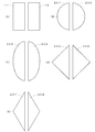
- (A) is a figure which shows the Example of the electrode shape of this invention, and is a figure which shows that it is a substantially rectangular shape.
- (B) is a figure which shows another Example of the electrode shape of this invention, and is a figure which shows that it is substantially circular.
- (C) is a figure which shows another Example of the electrode shape of this invention, and is a figure which shows that it is a substantially ellipse.
- (D) is a figure which shows another Example of the electrode shape of this invention, and is a figure which shows that four interior angles are substantially rhombus.
- (E) is a figure which shows another Example of the electrode shape of this invention, and is a figure which shows that it is a substantially rhombus shape in which four interior angles are not equal.
- (A) is a figure which shows another Example of the electrode shape of this invention, and is a figure which shows that it is a substantially rectangular parallelepiped.
- (B) is a figure which shows another Example of the electrode shape of this invention, and is a figure which shows that it is a shape which consists only of an outline part in a substantially rectangular parallelepiped.
- (C) is a figure which shows another Example of the electrode shape of this invention, and is a figure which shows that it is a substantially spherical body.
- (D) is a figure which shows another Example of the electrode shape of this invention, and is a figure which shows that it is a shape which consists only of an outline part by a substantially spherical body.
- (E) is a figure which shows another Example of the electrode shape of this invention, and is a figure which shows that it is a substantially cylinder.
- (F) is a figure which shows another Example of the electrode shape of this invention, and is a figure which shows that it is a shape which consists only of an outline part in a substantially cylindrical shape.
- (A) is a figure which shows another Example of the electrode shape of this invention, and is a perspective view which shows that it is the shape which bent the flat plate.
- (B) is a figure which shows another Example of the electrode shape of this invention, and is sectional drawing which shows that it is the shape which bent the flat plate.
- (C) is a figure which shows another Example of the electrode shape of this invention, and is a front view which shows that it is the shape which curved the flat plate.
- (D) It is a figure which shows another Example of the electrode shape of this invention, and is sectional drawing which shows that it is the shape which curved the flat plate.
- It is an equivalent circuit of embodiment shown in FIG. It is a figure which shows the transmission characteristic of the equivalent circuit shown in FIG. It is a figure which shows the structural example of the coupler for power transmission which concerns on embodiment of this invention.
- FIG. 10A is a perspective view which shows the example of the installation form of the radiation fin of the coupler for power transmission which concerns on embodiment of this invention.
- B is sectional drawing of the installation form shown to FIG. 10A.
- C is a figure which shows the example of another installation form of the radiation fin of the coupler for power transmission which concerns on embodiment of this invention. It is a figure which shows the example of the form of the insulation coating of the coupler for power transmission which concerns on embodiment of this invention.
- FIG. 3 is another embodiment of FIG. 1 in which the coupler electrodes are opposed to each other.
- 3 is another embodiment of FIG. 1 in which the coupler electrode has a cylindrical structure.
- 3 is another embodiment of FIG. 1 in which the coupler electrode has a cylindrical structure.
- FIG. 1 is a diagram for explaining the operation principle of the wireless power transmission system 1 according to the embodiment of the present invention. As shown in this figure, the wireless power transmission system 1 includes a power transmission device 10 and a power reception device 20.
- the power transmission device 10 includes electrodes 11 and 12, inductors 13 and 14, connection lines 15 and 16, and an AC power generation unit 17.
- the power receiving device 20 includes electrodes 21 and 22, inductors 23 and 24, connection lines 25 and 26, and a load 27.
- the electrodes 11 and 12 and the inductors 13 and 14 constitute a power transmission coupler.
- the electrodes 21 and 22 and the inductors 23 and 24 constitute a power receiving coupler.
- the electrodes 11 and 12 are made of a conductive member, and are arranged at a predetermined distance d1.
- the electrodes 11, 12, 21, and 22 flat plate electrodes having a rectangular shape having substantially the same size are illustrated.
- the electrode 11 and the electrode 21 are arranged in parallel so as to face each other with a distance d2, and the electrode 12 and the electrode 22 are also arranged in parallel so as to face each other with the same distance d2.
- the electrodes 11, 12, 21, and 22 may be electrodes having shapes other than those shown in FIG.
- electrodes having the following shapes can be used. That is, the substantially circular electrodes 201 and 202 as shown in FIG.
- the substantially elliptical electrodes 203 and 204 as shown in FIG. 2C, the substantially rhombic flat plate electrodes 205 and 206 as shown in FIGS. 2D and 2E, 207 and 208 may be used.
- the substantially prismatic electrodes 209 and 210 as shown in FIG. 3A, and the substantially prismatic interiors 211a and 212a as shown in FIG. 3B are hollow, and the electrodes 211 and 212 are formed of only the outer portions 211b and 212b.
- Electrodes 215 and 216 each consisting only of the outer portions 215b and 216b are shown as shown in FIG. Cylindrical electrodes 217 and 218, and electrodes 219 and 220 each having substantially cylindrical inner portions 219a and 220a as shown in FIG. 3F and having only outer portions 219b and 220b may be used.
- the flat electrodes 221 and 222 formed with the bent portions 221a and 222a as shown in the perspective view of FIG. 4A and the cross-sectional view of FIG. 4B, the perspective view of FIG. 4C and the curve as shown in the cross-sectional view of FIG.
- the electrodes 223 and 224 having the shapes described above may be used.
- the total width D including the distance d1 between the electrode 11 and the electrode 12 is set to be narrower than the near field indicated by ⁇ / 2 ⁇ where ⁇ is the wavelength of the electric field radiated from these electrodes. .
- the total width D including the distance d1 between the electrode 21 and the electrode 22 is set to be narrower than the near field indicated by ⁇ / 2 ⁇ .
- the length L of the electrode 11 and the electrode 12 is set to be narrower than the near field indicated by ⁇ / 2 ⁇ .
- the length L of the electrodes 21 and 22 is also set to be narrower than the near field indicated by ⁇ / 2 ⁇ .
- the distances d2 between the electrodes 11 and 21 and the electrodes 12 and 22 are also set to be shorter than the near field indicated by ⁇ / 2 ⁇ .
- the inductors 13 and 14 are configured by winding a conductive wire (for example, copper wire), and one end of each of the inductors 13 and 12 is electrically connected to the ends of the electrodes 11 and 12 in the example of FIG. .
- the connection line 15 is composed of a conductive wire (for example, copper wire) that connects the other end of the inductor 13 and one end of the output terminal of the AC power generation unit 17.
- the connection line 16 is formed of a conductive wire material that connects the other end of the inductor 14 and the other end of the output terminal of the AC power generation unit 17.
- the connection lines 15 and 16 are constituted by coaxial cables or balanced cables.
- the AC power generation unit 17 generates AC power having a predetermined frequency and supplies the AC power to the inductors 13 and 14 via the connection lines 15 and 16.
- the electrodes 21 and 22 are made of a conductive member, like the electrodes 11 and 12, and are arranged at a predetermined distance d1.
- the inductors 23 and 24 are configured by, for example, winding a conductive wire, and in the example of FIG. 1, one end of each of the electrodes 21 and 22 is electrically connected.
- the connection line 25 is composed of a conductive wire (for example, copper wire) that connects the other end of the inductor 23 and one end of the input terminal of the load 27.
- the connection line 26 is formed of a conductive wire that connects the other end of the inductor 24 and the other end of the input terminal of the load 27.
- the connection lines 25 and 26 are constituted by coaxial cables or balanced cables.
- the load 27 is supplied with electric power output from the AC power generation unit 17 and transmitted through the power transmission coupler and the power reception coupler.
- the load 27 is constituted by, for example, a rectifier and a secondary battery. Of course, it may be other than this.
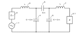
- FIG. 5 is a diagram showing an equivalent circuit of the wireless power transmission system 1 shown in FIG.
- the impedance 2 indicates the characteristic impedance of the connection lines 15 and 16 and the connection lines 25 and 26, and has a value of Z0.
- the inductor 3 corresponds to the inductors 13 and 14 and has an element value of L.
- the capacitor 4 has an element value (C ⁇ Cm) obtained by subtracting the capacitor having the element value Cm generated between the electrodes 11 and 12 and the electrodes 21 and 22 from the capacitor having the element value C generated between the electrodes 11 and 12.
- the capacitor 5 is a capacitor generated between the electrodes 11 and 12 and the electrodes 21 and 22, and has an element value of Cm.
- the capacitor 6 has an element value (C ⁇ Cm) obtained by subtracting a capacitor having an element value Cm generated between the electrodes 11 and 12 and the electrodes 21 and 22 from a capacitor having an element value C generated between the electrodes 21 and 22.
- the inductor 7 corresponds to the inductors 23 and 24 and has an element value of L.
- FIG. 6 shows the frequency characteristics of the S parameter between the power transmission device 10 and the power reception device 20.
- the horizontal axis of FIG. 6 indicates the frequency
- the vertical axis indicates the insertion loss (S21) from the power transmission device 10 to the power reception device 20.
- the insertion loss from the power transmitting device 10 to the power receiving device 20 has an anti-resonance point at the frequency fC and resonance points at the frequencies fL and fH.
- the frequency fC is determined by the inductance value L of the inductors 3 and 7 shown in FIG. 5 and the capacitance value C of the capacitor formed by the electrodes 11 and 12 or the electrodes 21 and 22.
- the frequencies fL and fH correspond to the inductance value L of the inductors 3 and 7 shown in FIG. 5, the capacitance value Cm of the capacitor formed by the electrodes 11 and 12 and the electrodes 21 and 22, and between the electrodes 11 and 12. And the capacitance value C of the capacitor generated between the electrodes 21 and 22, respectively.
- the frequency of the AC power generated by the AC power generator 17 is set to be approximately equal to the resonance frequency of the power transmission coupler constituted by the first and second electrodes 11 and 12 and the inductors 13 and 14. In this way, by setting the frequency of the AC power generation unit 17, it is possible to efficiently transmit power from the power transmission device 10 to the power reception device 20.
- the capacitance value C is determined by the electrode size, shape, and arrangement of the power transmission coupler and the power reception coupler.
- the capacitance value Cm depends on the distance d2 between the transmitting and receiving electrodes in addition to the electrode dimensions, shapes, and arrangement of each coupler.
- the input impedance seen from the AC power generation unit 17 side in the equivalent circuit of FIG. 5 varies depending on the electrode dimensions, shape, arrangement, and distance between the transmitting and receiving electrodes.
- the characteristic impedance Z0 on the AC power generation unit 17 side matches the input impedance, matching is achieved and power transmission efficiency is maximized, but the conditions depend on the electrode dimensions, shape, arrangement, and transmission / reception electrode distance of each coupler. It will be.
- the frequency of the AC power generated by the AC power generation unit 17 is based on various conditions such as the electrode dimensions, shape, arrangement, and distance between the transmitting and receiving electrodes of each coupler, and the frequency of the power from the transmitting coupler to the receiving coupler. You may set to the frequency where transmission efficiency becomes the maximum. By setting the frequency in this way, the transmission efficiency can be maximized.
- the electrodes 11 and 12 of the power transmission device 10 and the electrodes 21 and 22 of the power reception device 20 are coupled by electric field resonance, and the electrodes 11 and 12 of the power transmission device 10 are connected. AC power is transmitted to the electrodes 21 and 22 of the power receiving device 20 by an electric field.
- the electrodes 11 and 12 of the power transmission device 10 and the electrodes 21 and 22 of the power reception device 20 are arranged apart by a distance d2 shorter than ⁇ / 2 ⁇ that is the near field.
- the electrodes 21 and 22 are arranged in a region where the electric field component radiated from the electrodes 11 and 12 is dominant.
- the resonance frequency by the capacitor and inductors 13 and 14 formed between the electrodes 11 and 12 and the resonance frequency by the capacitor and inductors 23 and 24 formed between the electrodes 21 and 22 are set to be substantially equal. Has been.
- the electrodes 11 and 12 of the power transmission device 10 and the electrodes 21 and 22 of the power reception device 20 are coupled by electric field resonance, the electrodes 11 and 12 of the power transmission device 10 are changed to the electrodes 21 and 22 of the power reception device 20.
- AC power is efficiently transmitted by the electric field.
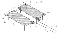
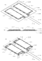
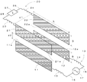
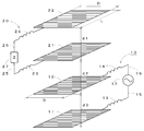
- FIGS. 7 and 8 are perspective views showing a configuration example of the embodiment of the present invention.
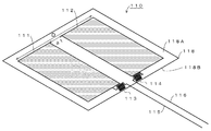
- FIG. 7 shows a configuration example of the power transmission coupler 110 according to the embodiment.
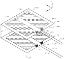
- FIG. 8 is a perspective view showing a state in which the power transmission coupler 110 and the power reception coupler 120 are arranged.
- the power transmission coupler 110 is configured by a conductive member having a rectangular shape on a front surface 118A of a circuit board 118 that is configured by an insulating member having a rectangular plate shape.
- the electrodes 111 and 112 to be arranged are arranged.
- no electrode or the like is arranged in the example of FIG.
- electrodes 111 and 112 are formed of a conductive thin film such as copper on a circuit board 118 formed of a glass epoxy board, a glass composite board, or the like.
- the electrodes 111 and 112 are arranged in parallel at positions separated by a predetermined distance d1.
- the width D of the electrodes 111 and 112 including the distance d1 is set to be narrower than the near field indicated by ⁇ / 2 ⁇ when the wavelength of the electric field radiated from these electrodes is ⁇ . .
- each of inductors 113 and 114 is connected to the ends of the electrodes 111 and 112 of the circuit board 118 in the short direction.
- the other ends of the inductors 113 and 114 are connected to one ends of connection lines 115 and 116, respectively.
- the connection lines 115 and 116 are disposed so as to avoid the regions of the electrodes 111 and 112 and the region sandwiched between them, and are disposed so as to extend in a direction away from these regions (lower right direction in FIG. 7). ing.
- connection lines 115 and 116 are configured by, for example, a coaxial cable or a balanced cable. Note that the other ends of the connection lines 115 and 116 are respectively connected to output terminals of an AC power generation unit (not shown). By connecting the AC power generation unit to the power transmission coupler 110 by the connection lines 115 and 116, a power transmission device is configured.
- the circuit board 118 does not have to be a rigid body, and may be a dielectric film such as polyimide. Since such a dielectric film has flexibility, the electrode part can be wound up or folded into a loose shape when not in use, and the transportability and storage property of the electrode part can be improved.
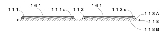
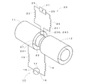
- FIG. 9 shows a configuration example of the power transmission coupler 110, and the electrodes 111 and 112 are fixed to the dielectric support post 141 by screws 142.
- the dielectric support post 141 is fixed to a not-shown coupler installation housing with a screw or the like. In such a configuration shown in FIG. 9, it is only necessary to install a number of dielectric columns 141 that can stably fix the electrodes 111 and 112 to the housing.
- a similar configuration can be applied to the power receiving side coupler.
- heat dissipation fins may be installed on the electrodes 111 and 112.
- the perspective view of FIG. 10A and the cross-sectional view of FIG. 10B are the heat dissipation fins 151 in which the surface area is increased by continuously forming uneven shapes in the surface direction on the surfaces 111a and 112a of the electrodes 111 and 112 in the configuration of FIG. The example which installed is shown.
- heat is mainly generated due to the AC resistance of the coils 113 and 114, but the generated heat can be released from the radiation fins 151 installed on the surfaces 111a and 112a of the electrodes 111 and 112. This configuration is effective for preventing thermal destruction of the coupler.
- FIG. 10C is an example in which heat radiation fins 151 are installed on the surfaces 111a and 112a of the electrodes 111 and 112 in the configuration of FIG. 9, and the electrodes 111 and 112 are fixed to the dielectric support posts 141 with screws 142. Similar effects can be obtained. 10A and 10C, the radiation fins 151 can be installed on the back surface opposite to the front surfaces 111a and 112a of the electrodes 111 and 112, respectively.
- a coolant may be enclosed inside the electrodes 111 and 112.
- a coolant may be enclosed inside the electrodes 111 and 112.
- the power can be reduced.
- heat is mainly generated due to the AC resistance of the coils 113 and 114, but the heat is dispersed on the exposed surfaces of the electrodes 211, 212, 215, 216, 219, and 220 by the convection of the coolant. Heat can be released from the surface.
- the electrodes 111 and 112 protect the surfaces 111a and 112a with a dielectric film.
- FIG. 11 shows an example in which the surfaces 111a and 112a, which are exposed surfaces of the electrodes 111 and 112, are coated in the configuration shown in FIG. 7, and shows a cross section of the circuit board 118 and the electrodes 111 and 112.
- the surfaces 111 a and 112 a that are exposed surfaces of the electrodes 111 and 112 are covered with the insulating film 161.
- the same coating can be applied to a configuration in which no dielectric substrate is present as shown in FIG. 9, and in this case, all exposed surfaces of the electrodes 111 and 112 may be covered with an insulating film.
- the power transmission coupler 110 constitutes a series resonance circuit including a capacitance C of a capacitor formed by disposing the electrodes 111 and 112 at a predetermined distance d1 and an inductor 1 and an inductance L of 13,114. These have a unique resonance frequency fC.
- the power receiving coupler 120 has the same configuration as that of the power transmitting coupler 110.
- electrodes 121 and 122 and inductors 123 and 124 made of a conductive member having a rectangular shape are arranged.
- Connection lines 125 and 126 are connected to the other ends of the inductors 123 and 124.
- the capacitance C of the capacitor formed by the electrodes 121 and 122 and the resonance frequency fC of the series resonance circuit by the inductance L of the inductors 123 and 124 are set to be substantially the same as those of the power transmission coupler 110.
- the connection lines 125 and 126 are configured by, for example, a coaxial cable or a balanced cable.
- a load (not shown) is connected to the other ends of the connection lines 125 and 126 of the power receiving coupler 120.
- a power receiving device is configured by connecting a load to the power receiving coupler 120 through the connection lines 125 and 126.
- FIG. 8 is a diagram showing a state in which the power transmission coupler 110 and the power reception coupler 120 are arranged to face each other. As shown in this figure, the power transmission coupler 110 and the power reception coupler 120 are arranged so that the circuit boards 118 and 128 are parallel to each other with a distance d2 so that the surfaces 118A and 128A of the circuit boards 118 and 128 face each other. Is done.
- the horizontal axis indicates the frequency (MHz) of AC power to be transmitted, and the vertical axis indicates transmission efficiency.
- a transmission efficiency of 80% or more is achieved around 25 MHz.
- the solid line indicates the frequency characteristic of the absolute value of the parameter S21
- the broken line indicates the frequency characteristic of the absolute value of the parameter S11.
- the parameter S11 indicates the reflection of the signal input from the power transmission coupler 110
- the parameter S21 indicates the passage of the signal from the power transmission coupler 110 to the power reception coupler 120.
- the value of the parameter S21 is about 0.9
- the value of the parameter S11 is about 0.1. Therefore, according to the present embodiment, it is understood that the signal input from the power transmission coupler 110 is transmitted to the power reception coupler 120 with less reflection near 27 MHz.
- 2 ) from the power transmission coupler 110 to the power reception coupler 120 when the power transmission coupler 110 and the power reception coupler 120 are arranged to be opposed to each other with a distance of 17 cm (d2 17 cm). It is a figure which shows the frequency characteristic. As shown in this figure, it can be seen that the transmission efficiency is about 80% when the frequency is around 27 MHz.
- the port impedance of the measuring instrument is set to a value equal to the characteristic impedance Z0 (real value) of the connection line.
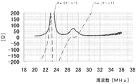
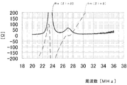
- Z0 real value
- Im [Zin1]) and the frequency characteristics of the real part (Re [Zin2]) and imaginary part (Im [Zin2]) of the impedance of the power receiving coupler 120 As shown in these figures, since the imaginary part of each impedance is substantially 0 near the resonance frequency of 27 MHz, power can be transmitted from the power transmission coupler 110 to the power reception coupler 120 with little loss. I understand.
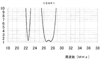
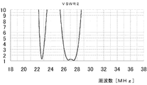
- VSWR Voltage
- d2 17 cm
- Standing Wave Ratio Standing Wave Ratio
- the voltage standing wave ratio between the power transmission coupler 110 and the power reception coupler 120 is approximately 1 in the vicinity of the resonance frequency of 27 MHz. Therefore, from the power transmission coupler 110 to the power reception coupler 120.
- impedance matching is established from the power receiving coupler 120 to the power receiving coupler 120, and power can be transmitted without reflection.
- the power transmission coupler 110 and the power reception coupler 120 are arranged, for example, about 17 cm apart, a transmission efficiency of about 80% can be achieved. Can be transmitted.
- the resistance component of the impedance is substantially 0, and the reflection is small.
- connection lines 115 and 116 and the connection lines 125 and 126 are arranged so as to avoid the regions of the electrodes 111 and 112 and the electrodes 121 and 122 and the region sandwiched between them.
- the area the area sandwiched between the electrodes 111 and 112 and the electrodes 121 and 122 in the example of FIG. 21
- the area is arranged so as to pass through the transmission. The characteristics deteriorate as shown in FIGS.
- connection lines 115 and 116 are disposed in the region sandwiched between the electrodes 111 and 112 and the connection lines 125 and 126 are disposed in the region sandwiched between the electrodes 121 and 122 as shown in FIG.
- the characteristics shown in FIG. 8 are degraded as shown in FIG. 23, and the peak transmission characteristics are reduced from about 0.8 to 0.7.
- connection lines 115 and 116 are arranged so as to pass immediately above or in the vicinity of the electrodes 111 and 112, the transmission characteristics deteriorate as in the case of FIG. Therefore, it is desirable to arrange the connection lines 115 and 116 at positions away from the electrodes 111 and 112 and to extend in a direction away from them. Of course, the same applies to the connection lines 125 and 126.
- the ends of the inductors 113 and 114 and the inductors 123 and 124 are connected to the ends of the electrodes 111 and 112 and the electrodes 121 and 122 that are close to each other. Connection of the lines 125 and 126 can be facilitated. Also, with such an arrangement, the connection lines 115 and 116 and the connection lines 125 and 126 can be arranged at positions away from the electrodes 111 and 112 and the electrodes 121 and 122, so that a reduction in transmission efficiency can be prevented. .
- the inductors 123 and 124 are arranged in a region sandwiched between the electrodes 111 and 112 and the electrodes 121 and 122, and the connection lines 115 and 116 and the connection lines 125 and 126 are arranged in the normal direction of the circuit board 118 and the circuit board 128. You may make it distract.
- the above embodiment is merely an example, and the present invention is not limited to the case described above.
- the electrodes 111 and 112 and the electrodes 121 and 122 have the same size, but they may have different sizes.
- the electrodes 121 and 122 may be smaller in size than the electrodes 111 and 112.
- the reverse configuration may be used.
- the electrodes 111 and 112 and the electrodes 121 and 122 are arranged to face each other.
- the electrodes 111 and 112 and the electrodes 121 and 122 are arranged so as to be shifted in the X direction or the Y direction shown in FIG. Also good.
- the power transmission coupler 110 and the power reception coupler 120 may be arranged so as to relatively rotate by a predetermined angle. In this case, as shown in FIG. 24, when the power transmission coupler 110 and the power reception coupler 120 are rotated 90 degrees or 270 degrees relative to each other, power is transmitted from the power transmission coupler 110 to the power reception coupler 120. It will not be transmitted.
- the capacitance between the electrode 21 and the electrode 11 is equal to the capacitance between the electrode 21 and the electrode 12, or the capacitance between the electrode 22 and the electrode 11 is equal to the capacitance between the electrode 22 and the electrode 12.
- the voltage excited by the power receiving coupler 120 is canceled out, it is desirable to adjust the positional relationship between the electrodes so that such a state does not occur. For example, if the mutual rotation angle is within ⁇ 15 degrees, a relative decrease in transmission efficiency due to rotation can be suppressed to less than 10%.
- the shapes of the electrodes 111 and 112 and the electrodes 121 and 122 may not be rectangular.
- the electrodes 111 and 112 and the electrodes 121 and 122 may be circular, elliptical, or rhombic flat plate electrodes as shown in FIGS. 2A to 2E, or prisms, spheres, cylinders as shown in FIGS. 3A to 3F.
- it may be a three-dimensional shape composed only of the outer portion thereof, or may be an electrode having a curved shape or a bent shape instead of a simple flat plate as shown in FIGS. 4A to 4D. . If the two electrodes have a constant distance to form a capacitor, there is essentially no difference between the electrode structure shown in FIG. 1 and the operating principle at the time of power transmission. It is.
- the inductors 113 and 114 and the inductors 123 and 124 are inserted between the electrodes 111 and 112 and the electrodes 121 and 122, the connection lines 115 and 116, and the connection lines 125 and 126. For example, it may be inserted in the vicinity of the AC power generation unit or the vicinity of the load.
- two inductors 113 and 114 and two inductors 123 and 124 are provided for the power transmission coupler 110 and the power reception coupler 120, respectively.
- one inductor is provided. Also good.
- the inductor is configured by winding a conductor wire in a cylindrical shape.
- the inductor has a shape meandering on a plane as used in a microstrip line. Further, it may be configured by a spiral shape on a plane.
- the inductor may be formed integrally with the electrodes 111 and 112 on the circuit board 118 or film.
- the coupler can be rolled up when not in use or folded into a loose shape, and the transportability and storage performance of the coupler can be improved.
- the power transmission coupler 110 and the power reception coupler 120 are used.
- a relay coupler 130 as shown in FIG. 25 may be used.
- the relay coupler 130 shown in FIG. 25 is configured by connecting the other ends of inductors 133 and 134 of a coupler having the same configuration as in FIG. Of course, these inductors 133 and 134 may have one configuration.
- the resonance frequency fC of the relay coupler 130 is set to be substantially the same as that of the power transmission coupler 110 and the power reception coupler 120.
- FIG. 26 shows a configuration example of a wireless power transmission system using such a relay coupler 130.
- a relay coupler 130 is disposed between the power transmission coupler 110 and the power reception coupler 120 in parallel with the two couplers. According to such a configuration, it is possible to efficiently transmit power farther than when the relay coupler 130 is not used.
- each electrode was arrange
- the same power transmission function as described above can be realized.
- FIG. 27 in the configuration shown in FIG.
- FIG. 28 shows a configuration in which the electrodes are opposed to each other while being spatially superimposed in the order of all the electrodes 11, 12, 21, and 22 in the configuration shown in FIG. 1. 27 and 28, it is possible to transmit electric power from the power transmission side to the power reception side through the electric field generated between the electrodes as in the configuration shown in FIG.
- the cylindrical structure 230 is formed by making the curved electrodes 11 and 12 face each other in the configuration shown in FIG. 1, and similarly, the curved electrodes 21 and 22 are made to face each other.
- a cylindrical structure 240 is formed, and by inserting the cylindrical structure 230 inside the cylindrical structure 240, a configuration in which these structures are arranged substantially concentrically is shown.
- the slit 231 that separates the electrodes 11 and 12 of the power transmission side coupler and the slit 241 that separates the electrodes 21 and 22 of the power reception side coupler are opposed to each other from the viewpoint of ensuring the coupling of the electric field. ing.
- power transmission can be performed even when the coupler is slid in the coaxial direction, so that it can be applied to applications such as robot arms and joints.
- the coupling capacitance between the couplers can be changed and the input impedance can be adjusted. Further, if one axial length of the cylindrical structure 230 of the power transmission side coupler and the cylindrical structure 240 of the power reception side coupler is reduced, the coupler having a reduced length slides relatively in the axial direction.
- the coupling capacity between the couplers does not change, the present invention can be applied to applications such as performing a certain amount of power transmission in a sliding mechanism system.
- the configuration is not limited to the configuration shown in FIG. 29, and it is only necessary that the cylindrical structures on both the power transmission side and the power reception side are arranged substantially concentrically. A cylindrical structure may be inserted.
- FIG. 30 in the configuration shown in FIG. 1, the electrodes 21 and 22 having a cylindrical shape smaller in diameter than the electrodes 11 and 12 are respectively concentric in the cylindrical electrodes 11 and 12.
- a configuration arranged in such a manner is shown.
- the slit 231 that separates the electrodes 11 and 12 of the power transmission side coupler and the slit 241 that separates the electrodes 21 and 22 of the power reception side coupler are opposed to each other from the viewpoint of securing coupling of the electric field. .
- FIG. 30 in the configuration shown in FIG.
- the electrode 11 and the electrode 12 are arranged symmetrically about the axis, and similarly, the electrode 21 and the electrode 22 are arranged for the axis, so that the power transmission side coupler and the power receiving unit are arranged. Even if the side coupler rotates relatively, the coupling capacity between the couplers does not change, so that the present invention can be applied to a purpose of transmitting a certain amount of power in the rotating mechanism system.
- a configuration in which each electrode has a trumpet-shaped opening or narrows toward the slits 231 and 241 can be applied.
- the diameters of the power receiving side electrodes 21 and 22 are smaller than the power transmitting side electrodes 11 and 12, but the configuration is not limited thereto.
- the power transmission side electrode may be arranged concentrically within the power reception side electrode.
- the above-described electrode configuration illustrated in FIGS. 27 to 30 is a form in which each of the electrodes 11 and 12 on the power transmission side and the electrodes 21 and 22 on the power reception side has a certain distance to form a capacitor. There is essentially no difference between the electrode configuration shown in Fig. 1 and the operating principle during power transmission. In any of the configurations illustrated in FIGS. 27 to 30, the electrode dimensions on the power transmission side and the power reception side can be set to different conditions as in the electrode configuration illustrated in FIG. 1.
Landscapes
- Engineering & Computer Science (AREA)
- Power Engineering (AREA)
- Computer Networks & Wireless Communication (AREA)
- Signal Processing (AREA)
- Charge And Discharge Circuits For Batteries Or The Like (AREA)
Abstract
電力を効率良く伝送できる無線電力伝送システムを提供すること。 送電装置は、第1および第2電極11,12と、第1および第2電極と交流電力発生部とを接続する第1および第2接続線15,16と、第1および第2電極と交流電力発生部の2つの出力端子の少なくとも一方の間に挿入される第1インダクタ13,14とを有し、受電装置は、合計幅が近傍界であるλ/2π以下の長さを有する第3および第4電極21,22と、第3および第4電極と負荷を接続する第3および第4接続線25,26と、第3および第4電極と負荷の2つの入力端子の少なくとも一方の間に挿入される第2インダクタ23,24と、を有し、第1および第2電極と第1インダクタによって構成されるカプラの共振周波数と、第3および第4電極と第2インダクタによって構成されるカプラの共振周波数が略等しくなるように設定される。
Description
本発明は、無線電力伝送システム、送電装置、および、受電装置に関するものである。
特許文献1には、電磁誘導を用いて、非接触の二つの電気回路間で電力の伝送を行う無線電力伝送装置が開示されている。
非特許文献1には、磁界共鳴、電界共鳴を用いて、非接触の二つの電気回路間で電力の伝送を行う無線電力伝送装置が開示されている。
非特許文献1には、磁界共鳴、電界共鳴を用いて、非接触の二つの電気回路間で電力の伝送を行う無線電力伝送装置が開示されている。
特許文献1に開示された技術では、電力を伝送するためのコイルにおける電力の損失が大きいため、電力を効率良く伝送できないという問題点がある。また、特許文献1に開示された技術では、同文献の段落(0058)などの記載から、電力を伝送できる距離が、数mmから数cmの範囲に限られるため、適用用途が限られる。
また、非特許文献1に開示された磁界共鳴を用いる方式では、電力を伝送できる距離を、数十cmから数mの範囲に拡大することが可能となるが、磁界を発生させ、共振を得るために導体を巻回したコイルを用いる必要がある。電力を伝送するにあたっては、このコイルに電流を流す必要があることから、導体損失を免れ得ない。また、コイルに用いる導体は一般に金属製の線材を用いることから、当該コイルを組み込んだ送受電装置の質量増加を招く。
また、非特許文献1に開示された電界共鳴を用いる方式では、共振に磁界ではなく電界を用いる。この方式によれば、共振にコイルは用いないが、共振が得られる電気長を導体線路により得る必要があるため、給電点および受電点からそれぞれ対称に1/4波長の長さの導体線路をミアンダ状に配置した電界結合用電極を用いる必要がある。このため、例えば共振周波数が低い場合には、共振を得るための電極の導体線路長が長くなる。また、空間的に隣接する導電線路間の干渉、すなわち線間結合による交流抵抗により、磁界共鳴と同様に導体損失を引き起こし、電力の伝送効率が悪くなる。特に、電極サイズを小さくするため電界結合用電極の導電線路間を狭くすると、線間結合による交流抵抗が増大する。
そこで、本発明は、非接触で電力を伝送できる距離を延長するとともに、電力を効率良く伝送できる無線電力伝送システム、送電装置、および、受電装置を提供することを目的としている。さらに、送電装置、および、受電装置の軽量化を可能とする。
上記課題を解決するために、本発明は、送電装置から受電装置に対して無線で交流電力を伝送する無線電力伝送システムにおいて、前記送電装置は、所定の距離を隔てて配置され、当該所定の距離を含む合計幅が近傍界であるλ/2π以下の長さを有する第1および第2電極と、前記第1および第2電極と交流電力発生部の2つの出力端子とをそれぞれ電気的に接続する第1および第2接続線と、前記第1および第2電極と前記交流電力発生部の2つの出力端子の少なくとも一方の間に挿入される第1インダクタと、を有し、前記受電装置は、所定の距離を隔てて配置され、当該所定の距離を含む合計幅が近傍界であるλ/2π以下の長さを有する第3および第4電極と、前記第3および第4電極と負荷の2つの入力端子とをそれぞれ電気的に接続する第3および第4接続線と、前記第3および第4電極と前記負荷の2つの入力端子の少なくとも一方の間に挿入される第2インダクタと、を有し、前記第1および第2電極と前記第1インダクタによって構成されるカプラの共振周波数と、前記第3および第4電極と前記第2インダクタによって構成されるカプラの共振周波数が略等しくなるように設定され、前記第1および第2電極と前記第3および第4電極は近傍界であるλ/2π以下の距離を隔てて配置される、ことを特徴とする。
このような構成によれば、電力を効率良く伝送することができる。
このような構成によれば、電力を効率良く伝送することができる。
また、他の発明は、上記発明に加えて、前記第1乃至第4電極は平板形状を有している。
このような構成によれば、設置スペースを少なくすることができる。
このような構成によれば、設置スペースを少なくすることができる。
また、他の発明は、上記発明に加えて、前記第1および第2電極と、前記第3および第4電極はそれぞれ同一平面上に配置されていることを特徴とする。
このような構成によれば、それぞれの電極を一体形成することにより、簡単に製造することができる。
このような構成によれば、それぞれの電極を一体形成することにより、簡単に製造することができる。
また、他の発明は、上記発明に加えて、前記第1および第3電極と、前記第2および第4電極は略平行に配置されていることを特徴とする。
このような構成によれば、設置スペースを少なくするとともに、電力の伝送効率を高めることができる。
このような構成によれば、設置スペースを少なくするとともに、電力の伝送効率を高めることができる。
また、他の発明は、上記発明に加えて、前記交流電力発生部の周波数は、前記第1および第2電極と前記第1インダクタによって構成されるカプラの共振周波数と略同じ周波数、または、2つの共振周波数のいずれか一方と略同じ周波数に設定されていることを特徴とする。
このような構成によれば、交流の周波数を共振周波数に合わせることにより、伝送効率を一層高めることができる。
このような構成によれば、交流の周波数を共振周波数に合わせることにより、伝送効率を一層高めることができる。
また、他の発明は、上記発明に加えて、前記交流電力発生部の周波数は、前記送電装置から前記受電装置への電力の伝送効率が最大となる周波数に設定されていることを特徴とする。
このような構成によれば、伝送効率を最大にすることができる。
このような構成によれば、伝送効率を最大にすることができる。
また、他の発明は、上記発明に加えて、前記第1インダクタは、前記第1電極と前記第1接続線の間に挿入されたインダクタと、前記第2電極と前記第2接続線の間に挿入されたインダクタの2つを有し、前記第2インダクタは、前記第3電極と前記第3接続線の間に挿入されたインダクタと、前記第4電極と前記第4接続線の間に挿入されたインダクタの2つを有する、ことを特徴とする。
このような構成によれば、設計を容易に行うことができる。
このような構成によれば、設計を容易に行うことができる。
また、他の発明は、上記発明に加えて、前記第1および第2接続線は、前記第1および第2電極の領域およびこれらによって挟まれた領域を回避するように配置されるとともに、当該領域から遠ざかる方向に伸延されていることを特徴とする。
このような構成によれば、接続線と電極との間の干渉を防ぐことにより、伝送効率を高めることができる。
このような構成によれば、接続線と電極との間の干渉を防ぐことにより、伝送効率を高めることができる。
また、他の発明は、上記発明に加えて、前記第3および第4接続線は、前記第3および第4電極の領域およびこれらによって挟まれた領域を回避するように配置されるとともに、当該領域から遠ざかる方向に伸延されていることを特徴とする。
このような構成によれば、接続線と電極との間の干渉を防ぐことにより、伝送効率を高めることができる。
このような構成によれば、接続線と電極との間の干渉を防ぐことにより、伝送効率を高めることができる。
また、他の発明は、上記発明に加えて、所定の距離を隔てて配置され、当該所定の距離を含む合計幅が近傍界であるλ/2π以下の長さを有する第5および第6電極と、前記第5および第6電極の間に接続された第3インダクタと、を有する中継装置を備え、前記第5および第6電極は、前記送電装置の前記第1および第2電極と、前記受電装置の前記第3および第4電極の間に配置されるとともに、前記第5および第6電極と前記第3インダクタによって構成されるカプラの共振周波数が、前記送電装置および前記受電装置のカプラの共振周波数と略等しくなるように設定されていることを特徴とする。
このような構成によれば、より遠い距離まで効率良く電力を伝送することができる。
このような構成によれば、より遠い距離まで効率良く電力を伝送することができる。
また、他の発明は、上記発明に加えて、前記第1および第2電極は、湾曲形状を有しており、対向させることで第1の筒状構造をなしており、前記第3および第4電極は、湾曲形状を有しており、対向させることで第2の筒状構造をなしており、前記第1および第2電極を離間するスリットと、前記第3および第4電極を離間するスリットとが対向するように、前記第1および第2の筒状構造が略同心円状に配置されていることを特徴とする。
このような構成によれば、カプラを同軸方向にスライドさせても電力伝送を行うことができる。
このような構成によれば、カプラを同軸方向にスライドさせても電力伝送を行うことができる。
また、他の発明は、上記発明に加えて、前記第1および第2電極の暴露面に絶縁被覆を施し、前記第3および第4電極の暴露面に絶縁被覆を施したことを特徴とする。
このような構成によれば、電極の腐食による電力伝送効率の低下を抑えることができるとともに、電極からの放電を防止することができる。
このような構成によれば、電極の腐食による電力伝送効率の低下を抑えることができるとともに、電極からの放電を防止することができる。
また、本発明は、送電装置から受電装置に対して無線で交流電力を伝送する無線電力伝送システムの前記送電装置において、所定の距離を隔てて配置され、当該所定の距離を含む合計幅が近傍界であるλ/2π以下の長さを有する第1および第2電極と、前記第1および第2電極と交流電力発生部の2つの出力端子とをそれぞれ電気的に接続する第1および第2接続線と、前記第1および第2電極と前記交流電力発生部の2つの出力端子の少なくとも一方の間に挿入される第1インダクタと、を有し、前記第1および第2電極と前記第1インダクタによって構成されるカプラの共振周波数は、前記受電装置が有する第3および第4電極と第2インダクタによって構成されるカプラの共振周波数と略等しくなるように設定され、前記第1および第2電極と前記第3および第4電極は近傍界であるλ/2π以下の距離を隔てて配置される、ことを特徴とする。
このような構成によれば、電力を効率良く伝送することができる。
このような構成によれば、電力を効率良く伝送することができる。
また、本発明は、送電装置から受電装置に対して無線で交流電力を伝送する無線電力伝送システムの前記受電装置において、所定の距離を隔てて配置され、当該所定の距離を含む合計幅が近傍界であるλ/2π以下の長さを有する第3および第4電極と、前記第3および第4電極と負荷の2つの入力端子とをそれぞれ電気的に接続する第3および第4接続線と、前記第3および第4電極と前記負荷の2つの入力端子の少なくとも一方の間に挿入される第2インダクタと、を有し、前記第3および第4電極と前記第2インダクタによって構成されるカプラの共振周波数は、前記送電装置が有する第1および第2電極と第1インダクタによって構成されるカプラの共振周波数と略等しくなるように設定され、前記第1および第2電極と前記第3および第4電極は近傍界であるλ/2π以下の距離を隔てて配置される、ことを特徴とする。
このような構成によれば、電力を効率良く伝送することができる。
このような構成によれば、電力を効率良く伝送することができる。
本発明によれば、電力を効率良く伝送できる無線電力伝送システム、送電装置、および、受電装置を提供することが可能となる。
次に、本発明の実施形態について説明する。
(A)実施形態の動作原理の説明
図1は、本発明の実施形態に係る無線電力伝送システム1の動作原理を説明するための図である。この図に示すように、無線電力伝送システム1は、送電装置10、および、受電装置20を有している。
図1は、本発明の実施形態に係る無線電力伝送システム1の動作原理を説明するための図である。この図に示すように、無線電力伝送システム1は、送電装置10、および、受電装置20を有している。
ここで、送電装置10は、電極11,12、インダクタ13,14、接続線15,16、および、交流電力発生部17を有している。また、受電装置20は、電極21,22、インダクタ23,24、接続線25,26、および、負荷27を有している。電極11,12およびインダクタ13,14は送電用カプラを構成する。電極21,22およびインダクタ23,24は受電用カプラを構成する。
ここで、電極11,12は、導電性を有する部材によって構成され、所定の距離d1を隔てて配置されている。図1の例では、電極11,12,21,22として、略同一のサイズを有する矩形形状を有する平板状の電極が例示されている。また、電極11と電極21は距離d2を隔てて対向するように平行に配置され、電極12と電極22も同じ距離d2を隔てて対向するように平行に配置されている。なお、電極11,12,21,22としては、図1に示す以外の形状の電極であってもよい。例えば、図2Aに示すような平板矩形状の電極11、12以外にも、例えば、次のような形状の電極を用いることが可能である。すなわち、図2Bに示すような略円形状の電極201、202、図2Cに示すような略楕円形状の電極203、204、図2Dおよび図2Eに示すような略ひし形の平板電極205、206、207、208を用いてもよい。また、図3Aに示すような略角柱状の電極209、210、図3Bに示すような略角柱内部211a、212aがそれぞれ中空であって外郭部211b、212bのみからなる電極211、212、図3Cに示すような略球形の電極213、214、図3Dに示すような略球形内部215a、216aがそれぞれ中空であって外郭部215b、216bのみからなる電極215、216、図3Eに示すような略円柱状の電極217、218、図3Fに示すような略円柱内部219a、220aがそれぞれ中空であって外郭部219b、220bのみからなる電極219、220を用いてもよい。さらに、図4Aの斜視図および図4Bの断面図に示すような屈曲部221a、222aが形成された平板状の電極221、222、図4Cの斜視図および図4Dの断面図に示すような湾曲した形状の電極223、224を用いてもよい。
図1乃至図4Dに示した構成例のうち、以下では図1に示す形状の電極を用いた構成例について説明する。電極11および電極12の距離d1を含む合計幅Dは、これらの電極から放射される電界の波長をλとした場合に、λ/2πで示される近傍界よりも狭くなるように設定されている。同様に、電極21および電極22の距離d1を含む合計幅Dは、λ/2πで示される近傍界よりも狭くなるように設定されている。また、電極11および電極12の長さLは、λ/2πで示される近傍界よりも狭くなるように設定されている。電極21および電極22の長さLも、λ/2πで示される近傍界よりも狭くなるように設定されている。電極11と電極21および電極12と電極22の間の距離d2についても、λ/2πで示される近傍界よりも短くなるように設定されている。
インダクタ13,14は、例えば、導電性の線材(例えば、銅線)を巻回して構成され、図1の例では、電極11,12の端部にそれぞれの一端が電気的に接続されている。接続線15はインダクタ13の他端と交流電力発生部17の出力端子の一端とを接続する導電性の線材(例えば、銅線)によって構成される。接続線16はインダクタ14の他端と交流電力発生部17の出力端子の他端とを接続する導電性の線材によって構成される。なお、接続線15,16は、同軸ケーブルまたは平衡ケーブルによって構成される。
交流電力発生部17は、所定の周波数の交流電力を発生し、接続線15,16を介してインダクタ13,14に供給する。
電極21,22は、電極11,12と同様に、導電性を有する部材によって構成され、所定d1の距離を隔てて配置されている。
インダクタ23,24は、例えば、導電性の線材を巻回して構成され、図1の例では、電極21,22の端部にそれぞれの一端が電気的に接続されている。接続線25はインダクタ23の他端と負荷27の入力端子の一端とを接続する導電性の線材(例えば、銅線)によって構成される。接続線26はインダクタ24の他端と負荷27の入力端子の他端とを接続する導電性の線材によって構成される。なお、接続線25,26は、同軸ケーブルまたは平衡ケーブルによって構成される。
負荷27は、交流電力発生部17から出力され、送電用カプラおよび受電用カプラを介して伝送された電力が供給される。なお、負荷27は、例えば、整流装置および二次電池等によって構成されている。もちろん、これ以外であってもよい。
図5は、図1に示す無線電力伝送システム1の等価回路を示す図である。この図5において、インピーダンス2は、接続線15,16および接続線25,26の特性インピーダンスを示し、Z0の値を有している。インダクタ3はインダクタ13,14に対応し、Lの素子値を有している。キャパシタ4は、電極11,12の間に生じる素子値Cのキャパシタから、電極11,12と電極21,22の間に生じる素子値Cmのキャパシタを減じた素子値(C-Cm)を有する。キャパシタ5は、電極11,12と電極21,22の間に生じるキャパシタを示し、Cmの素子値を有している。キャパシタ6は、電極21,22の間に生じる素子値Cのキャパシタから、電極11,12と電極21,22の間に生じる素子値Cmのキャパシタを減じた素子値(C-Cm)を有する。インダクタ7はインダクタ23,24に対応し、Lの素子値を有している。
図6は、送電装置10と受電装置20の間のSパラメータの周波数特性を示している。具体的には、図6の横軸は周波数を示し、縦軸は送電装置10から受電装置20への挿入損失(S21)を示している。この図6に示すように、送電装置10から受電装置20への挿入損失は、周波数fCで反共振点を有し、周波数fLおよびfHで共振点を有している。ここで、周波数fCは、図5に示すインダクタ3,7のインダクタンス値Lと、電極11,12または電極21,22によって形成されるキャパシタのキャパシタンス値Cによって定まる。また、周波数fLおよびfHは、図5に示すインダクタ3,7のインダクタンス値Lと、電極11,12および電極21,22によって形成されるキャパシタのキャパシタンス値Cmと、ならびに、電極11,12の間および電極21,22の間にそれぞれ生じるキャパシタのキャパシタンス値Cによって定まる。
交流電力発生部17が発生する交流電力の周波数は、第1および第2電極11、12とインダクタ13、14によって構成される送電用カプラの共振周波数と略等しくなるように設定される。このように、交流電力発生部17の周波数を設定することにより、送電装置10から受電装置20に対して効率よく電力を送電することができる。
また、上記キャパシタンス値Cは、送電用カプラと受電用カプラとのそれぞれの電極寸法、形状、配置で決まる。キャパシタンス値Cmは、各カプラの電極寸法、形状、配置に加えて送受電極間の距離d2に依存する。このため、図5の等価回路における交流電力発生部17側からみた入力インピーダンスは、電極寸法、形状、配置、及び送受電極間距離で変化することになる。交流電力発生部17側の特性インピーダンスZ0と入力インピーダンスが一致すると整合が取れ、電力伝送効率が最大になるが、その条件は各カプラの電極寸法、形状、配置、及び送受電極間距離に依存することになる。
したがって、交流電力発生部17が発生する交流電力の周波数は、各カプラの電極寸法、形状、配置、及び送受電極間距離などの諸条件に基づいて、送電用カプラから受電用カプラへの電力の伝送効率が最大となる周波数に設定してもよい。このように周波数を設定することで、伝送効率を最大にすることができる。
以上のような構成からなる図1に示す実施形態では、送電装置10の電極11,12と受電装置20の電極21,22は、電界共振結合されており、送電装置10の電極11,12から受電装置20の電極21,22に対して電界によって交流電力が伝送される。
つまり、図1に示す実施形態では、送電装置10の電極11,12と受電装置20の電極21,22は、近傍界であるλ/2πよりも短い距離d2だけ隔てて配置されているので、電極11,12から放射される電界成分が支配的である領域に電極21,22が配置される。また、電極11,12の間に形成されるキャパシタおよびインダクタ13,14による共振周波数と、電極21,22の間に形成されるキャパシタおよびインダクタ23,24による共振周波数とは略等しくなるように設定されている。このように、送電装置10の電極11,12と受電装置20の電極21,22は、電界共振結合されていることから、送電装置10の電極11,12から受電装置20の電極21,22に対して電界によって交流電力が効率よく伝送される。
(B)実施形態の構成の説明
図7,8は、本発明の実施形態の構成例を示す斜視図である。ここで、図7は、実施形態に係る送電用カプラ110の構成例を示している。また、図8は送電用カプラ110と受電用カプラ120とを配置した状態を示す斜視図である。
図7,8は、本発明の実施形態の構成例を示す斜視図である。ここで、図7は、実施形態に係る送電用カプラ110の構成例を示している。また、図8は送電用カプラ110と受電用カプラ120とを配置した状態を示す斜視図である。
図7に示すように、送電用カプラ110は、矩形の板状形状を有する絶縁部材によって構成される回路基板118の表(おもて)面118A上に、矩形形状を有する導電性部材によって構成される電極111,112が配置されて構成される。回路基板118の裏面118Bには、この図7の例では、電極等は配置されていない。具体的な構成例としては、例えば、ガラスエポキシ基板やガラスコンポジット基板等によって構成される回路基板118上に、銅等の導電性の薄膜によって電極111,112が形成される。電極111,112は、所定の距離d1だけ離れた位置に平行に配置されている。また、距離d1を含む電極111,112の幅Dは、これらの電極から放射される電界の波長をλとした場合に、λ/2πで示される近傍界よりも狭くなるように設定されている。
回路基板118の電極111,112の短手方向の端部には、インダクタ113,114の一端がそれぞれ接続されている。また、インダクタ113,114の他端は、接続線115,116の一端にそれぞれ接続されている。接続線115,116は、電極111,112の領域およびこれらに挟まれる領域を回避するように配置されるとともに、これらの領域から遠ざかる方向(図7の右下方向)に伸延するように配置されている。より詳細には、電極111,112のそれぞれの矩形領域と、これら2つの電極111,112によって挟まれた領域を回避して配置されるとともに、これらの領域から遠ざかる方向に伸延するように配置されている。このように配置することで、電極111,112と接続線115,116の間の干渉を少なくすることができるので、伝送効率の低下を防止できる。接続線115,116は、例えば、同軸ケーブルまたは平衡ケーブルによって構成されている。なお、接続線115,116の他端は、図示しない交流電力発生部の出力端子にそれぞれ接続されている。接続線115,116によって送電用カプラ110に交流電力発生部が接続されることにより、送電装置が構成される。
なお、回路基板118は剛体である必要は無く、たとえばポリイミドなどの誘電体フィルムであってもよい。このような誘電体フィルムは可撓性を有するので、未使用時に電極部を巻き上げる、あるいはじゃばら状に折りたたむことが可能となり、電極部の搬送性および収納性を高めることが可能となる。
また、電極に剛性を持たせ、回路基板118などの支持基板無しで筐体に固定することも可能である。図9は送電用カプラ110の構成例であり、電極111、112は誘電体支柱141にねじ142により固定されている。誘電体支柱141は図示しないカプラ設置筐体にねじ等で固定される構成である。このような図9に示す構成では、電極111、112が安定して筐体に固定可能な数の誘電体支柱141を設置すればよい。同様の構成を受電側カプラにも適用することができる。
また、電力伝送時の放熱対策として、電極111、112に放熱用のフィンを設置してもよい。図10Aの斜視図と図10Bの断面図は、図7の構成において、電極111、112の表面111a、112aに、面方向に凹凸形状が連続的に形成することで表面積を広げた放熱フィン151を設置した例を示している。電力伝送時において主にコイル113、114の交流抵抗に起因して熱が発生するが、発生した熱を電極111、112の表面111a、112aに設置された放熱フィン151から逃がすことができる。この構成はカプラの熱破壊防止に効果がある。図10Cは図9の構成において、電極111、112の表面111a、112aに放熱フィン151を設置し、誘電体支柱141に電極111、112をねじ142により固定した例であり、図10Aの構成と同様の効果を得ることができる。図10Aおよび図10Cの構成において、放熱フィン151は電極111,112の表面111a、112aと反対の裏面に設置することも可能である。
さらに別の放熱対策として、電極111、112の内部に冷却材を封入しても良い。例えば、上述した図3B、図3D、図3F等に示したような外郭部のみからなる立体構造の電極211、212、215、216、219、220の内部に冷却材を封入することで、電力伝送時において主にコイル113、114の交流抵抗に起因して熱が発生するが、その熱を冷却材の対流により電極211、212、215、216、219、220の暴露面に分散させ、暴露面から熱を逃がすことができる。
また腐食対策として、電極111、112は誘電体皮膜にて表面111a、112aを保護するのが望ましい。図7および図9に示す送電側カプラにおいて、電極部111,112の暴露面にレジスト材料等により絶縁被覆を施せば、電極111,112の腐食による電力伝送効率の低下を防ぐことができる。図11は、図7に示した構成において電極111,112の暴露面である表面111a、112aに被覆を施した場合の例であり、回路基板118及び電極111,112の断面を示している。すなわち、電極111、112の暴露面である表面111a、112aが絶縁膜161で覆われている。同様の被覆は、図9に示したような誘電体基板が存在しない構成においても適用可能であり、この場合には電極111、112の暴露面全てを絶縁膜で被覆すればよい。また、図10Aおよび図10Cに示す放熱フィン151が電極111、112に設置された場合においても、電極111、112が放熱フィン151から外れて暴露している箇所を絶縁膜で被覆する、あるいは電極111、112及び放熱フィン151丸ごと絶縁膜で被覆することで、電極111、112の腐食による電力伝送効率の低下を抑えることができる。また、電極111、112を絶縁膜161で被覆することで、電極111、112との間に大きな電圧が印加されても、電極111、112の表面からの放電の発生を抑えることができる。なお、図3A乃至図3Fに示したように電極が立体構造となる場合においても絶縁膜で被覆することは可能である。
送電用カプラ110は、電極111,112が所定の距離d1を隔てて配置されることによって形成されるキャパシタのキャパシタンスCと、インダクタ1を13,114のインダクタンスLによる直列共振回路を構成するので、これらによる固有の共振周波数fCを有している。
受電用カプラ120は、送電用カプラ110と同様の構成とされ、回路基板128の表面128A上に、矩形形状を有する導電性部材によって構成される電極121,122およびインダクタ123,124が配置され、インダクタ123,124の他端に接続線125,126が接続されて構成される。電極121,122によって形成されるキャパシタのキャパシタンスCと、インダクタ123,124のインダクタンスLによる直列共振回路の共振周波数fCは送電用カプラ110と略同じに設定される。接続線125,126は、例えば、同軸ケーブルまたは平衡ケーブルによって構成されている。受電用カプラ120の接続線125,126の他端には、図示しない負荷が接続される。接続線125,126によって受電用カプラ120に負荷が接続されることにより、受電装置が構成される。
図8は、送電用カプラ110と受電用カプラ120を対向配置した状態を示す図である。この図に示すように、送電用カプラ110と受電用カプラ120は、回路基板118,128の表面118A,128Aが対向するように距離d2を隔て、回路基板118,128が平行になるように配置される。
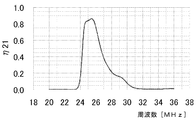
つぎに、図8に示す実施形態の動作について説明する。図12は、図8に示す実施形態の送電用カプラ110と受電用カプラ120を14cm隔てて対向配置した場合(d2=14cmの場合)における送電用カプラ110から受電用カプラ120への伝送効率η21(=|S21|2)の周波数特性を示す図である。この図において横軸は伝送する交流電力の周波数(MHz)を示し、縦軸は伝送効率を示している。図12に示す例では、25MHz周辺において、伝送効率80%以上を達成していることが分かる。
図13は、送電用カプラ110と受電用カプラ120を17cm隔てて対向配置した場合(d2=17cmの場合)における送電用カプラ110と受電用カプラ120の間のSパラメータの周波数特性を示す図である。この図において、実線はパラメータS21の絶対値の周波数特性を示し、破線はパラメータS11の絶対値の周波数特性を示している。ここで、パラメータS11は送電用カプラ110から入力した信号の反射を示し、パラメータS21は送電用カプラ110から受電用カプラ120への信号の通過を示す。この図13に示すように、27MHz付近では、パラメータS21の値は0.9程度であり、また、パラメータS11の値は0.1程度である。したがって、本実施形態によれば、27MHz付近では、送電用カプラ110から入力した信号は、少ない反射で受電用カプラ120に伝送されることが分かる。
図14は、送電用カプラ110と受電用カプラ120を17cm隔てて対向配置した場合(d2=17cmの場合)における送電用カプラ110から受電用カプラ120への伝送効率η21(=|S21|2)の周波数特性を示す図である。この図に示すように、周波数が27MHz付近では80%程度の伝送効率を有していることが分かる。
図15,16は、送電用カプラ110と受電用カプラ120を17cm隔てて対向配置した場合(d2=17cmの場合)における送電用カプラ110のインピーダンスS11と、受電用カプラ120のインピーダンスS22のスミスチャートを示している。この場合、測定器のポートインピーダンスは接続線路の特性インピーダンスZ0(実数値)と等しい値に設定している。これらの図に示すように、本実施形態では、送電用カプラ110および受電用カプラ120のインピーダンスの軌跡は、スミスチャートの円の中心付近を通過することから、この付近において伝送を行うように設定することにより反射を抑えて効率良く電力を伝送することができる。
図17,18は、送電用カプラ110と受電用カプラ120を17cm隔てて対向配置した場合(d2=17cmの場合)における送電用カプラ110のインピーダンスの実部(Re[Zin1])と虚部(Im[Zin1])と、受電用カプラ120のインピーダンスの実部(Re[Zin2])と虚部(Im[Zin2])のそれぞれの周波数特性を示す図である。これらの図に示すように、それぞれのインピーダンスの虚部は、共振周波数である27MHz付近において略0となっていることから、送電用カプラ110から受電用カプラ120へ少ない損失で電力を伝送できることが分かる。
図19,20は、送電用カプラ110と受電用カプラ120を17cm隔てて対向配置した場合(d2=17cmの場合)における送電用カプラ110と受電用カプラ120の電圧定在波比(VSWR(Voltage Standing Wave Ratio))をそれぞれ示している。これらの図に示すように、送電用カプラ110と受電用カプラ120の電圧定在波比は、共振周波数である27MHz付近において略1となっていることから、送電用カプラ110から受電用カプラ120、または、受電用カプラ120から受電用カプラ120へはインピーダンスの整合が取れており、反射なく電力を伝送することができることが分かる。
以上に説明したように、本実施形態では、送電用カプラ110と受電用カプラ120を、例えば、17cm程度離して配置した場合、80%程度の伝送効率を達成することができることから、効率よく電力を伝送することができる。また、共振周波数においては、インピーダンスの抵抗成分が略0となり、また、反射も少ないことが分かる。
なお、図8に示す実施形態では、接続線115,116および接続線125,126を、電極111,112および電極121,122の領域およびこれらによって挟まれた領域を回避するように配置したが、例えば、図21に示すように、当該領域(図21の例では電極111,112および電極121,122に挟まれた領域)を回避せずに、当該領域を通過するように配置した場合、伝送特性が図22から図23に示すように劣化する。すなわち、図21に示すように接続線115,116を電極111,112に挟まれた領域に配置するとともに、接続線125,126を電極121,122に挟まれた領域に配置した場合、図22に示す特性(図8に示すように配置した場合の特性)が、図23に示すように劣化し、ピークの伝送特性が0.8から0.7程度に低下する。
なお、接続線115,116を電極111,112の直上または近傍を通過するように配置した場合も、図21の場合と同様に伝送特性が劣化する。したがって、接続線115,116については、電極111,112から離れた位置に配置するとともに、これらから離れる方向に伸延するように配置することが望ましい。もちろん、接続線125,126についても同様である。
すなわち、本実施形態では、電極111,112および電極121,122の相互に近接する端部にインダクタ113,114およびインダクタ123,124の一端を接続するようにしたので、接続線115,116および接続線125,126の接続を容易にすることができる。また、このような配置により、接続線115,116および接続線125,126を電極111,112および電極121,122から離れた位置に配置することが可能になるので、伝送効率の低下を防止できる。なお、電極111,112および電極121,122に挟まれた領域にインダクタ123,124を配置するとともに、回路基板118および回路基板128の法線方向に接続線115,116および接続線125,126を伸延するようにしてもよい。
(C)変形実施形態の説明
以上の実施形態は一例であって、本発明が上述したような場合のみに限定されるものでないことはいうまでもない。例えば、以上の実施形態では、電極111,112および電極121,122は同じサイズを有するようにしたが、これらが異なるサイズを有するようにしてもよい。具体的には、電極121,122が電極111,112よりも小さいサイズになるようにしてもよい。もちろん、その逆の構成でもよい。
以上の実施形態は一例であって、本発明が上述したような場合のみに限定されるものでないことはいうまでもない。例えば、以上の実施形態では、電極111,112および電極121,122は同じサイズを有するようにしたが、これらが異なるサイズを有するようにしてもよい。具体的には、電極121,122が電極111,112よりも小さいサイズになるようにしてもよい。もちろん、その逆の構成でもよい。
また、以上の実施形態では、電極111,112および電極121,122を対向配置するようにしたが、例えば、これらが図8に示すX方向またはY方向にずれた状態で配置されるようにしてもよい。あるいは、送電用カプラ110と受電用カプラ120が所定の角度だけ相対的に回転するように配置してもよい。なお、その場合において、図24に示すように、送電用カプラ110と受電用カプラ120が相互に90度または270度回転配置された場合には、送電用カプラ110から受電用カプラ120に電力が伝送されなくなる。すなわち、電極21と電極11の間の容量と、電極21と電極12の間の容量が等しいか、または、電極22と電極11の間の容量と、電極22と電極12の間の容量が等しい場合には、受電用カプラ120に励起された電圧が相殺されるので、このような状態にならないように電極同士の位置関係を調整することが望ましい。例えば、相互の回転角度が±15度以内に収まれば、回転に伴う伝送効率の相対的な低下を10%未満に抑えることができる。
以上の構成において、電極111,112および電極121,122の形状は、矩形形状ではなくてもよい。例えば、電極111、112及び電極121、122の形状が図2A-図2Eに示すような円形または楕円形状またはひし形の平板電極であったり、図3A-図3Fに示すような角柱、球、円柱、あるいはそれらの外郭部だけからなる立体形状であってもよい、また、図4A-図4Dに示すような単なる平板ではなく平板が湾曲した形状または屈曲した形状の電極であったりしてもよい。2つの電極が一定の距離を有してキャパシタを形成する形態であれば、図1に示す電極構造の場合と電力伝送時の動作原理において本質的に差は生じないため、本発明に適用可能である。
また、インダクタ113,114およびインダクタ123,124については、電極111,112および電極121,122と接続線115,116および接続線125,126の間に挿入するようにしたが、これ以外の場所(例えば、交流電力発生部の近傍または負荷の近傍)に挿入することも可能である。また、以上の実施形態では、送電用カプラ110および受電用カプラ120に対してそれぞれ2つずつのインダクタ113,114およびインダクタ123,124を設けるようにしたが、インダクタを1つずつ設けるようにしてもよい。
また、以上の実施形態では、インダクタとしては、導体線を円柱状に巻回して構成するようにしたが、例えば、マイクロストリップラインで使用されるような、平面上を蛇行する形状を有するものや、平面上で螺旋形状を有するものによって構成するようにしてもよい。
また、インダクタは、回路基板118、又はフィルム上に電極111、112と一体形成されたものでもよい。この場合、コネクタ接続部分を除き、カプラを未使用時に巻き上げる、あるいはじゃばら状に折りたたむことが可能となり、カプラの搬送性および収納性を高めることが可能となる。
また、以上の実施形態では、送電用カプラ110と受電用カプラ120による構成としたが、図25に示すような、中継用カプラ130を有する構成としてもよい。図25に示す中継用カプラ130は、図7と同様の構成を有するカプラのインダクタ133,134の他端同士が接続線135によって接続されて構成されている。もちろん、これらのインダクタ133,134を1つの構成としてもよい。なお、この中継用カプラ130の共振周波数fCは、送電用カプラ110および受電用カプラ120と略同じになるように設定される。図26は、このような中継用カプラ130を用いた無線電力伝送システムの構成例を示している。この例では、送電用カプラ110と受電用カプラ120の間に中継用カプラ130が2つのカプラと平行に配置されている。このような構成によれば、中継用カプラ130を用いない場合に比較して、より遠くまで効率よく電力を伝送することができる。
また、以上の実施形態では送電側および受電側でそれぞれの電極が略平行もしくはそれに順ずる配置となっている場合について説明したが、図1に示すような送電側の電極11、12と受電側の電極21、22がそれぞれ面方向で対向する配置以外にも、例えば、送電側、及び受電側でそれぞれの電極のエッジを対向させても、上記と同様の電力伝送機能を実現することができる。例えば、図27では、図1に示した構成において、送電側の電極11、12を対向させ、受電側の電極21、22を対向させ、さらに、電極11のエッジ11aと電極21のエッジ21aとが距離d2を隔てて対向するように配置し、電極12のエッジ12aと電極22のエッジ22aとが同じ距離d2を隔てて対向するように配置した構成を示している。また、図28は、図1に示した構成において、全ての電極11、12、21、22の順番で空間的に重畳させながら各電極を対向させた構成を示している。このような図27および図28に示すような構成においても、図1で示した構成と同様に電極間に生じる電界を通じて、送電側から受電側に電力を伝送することが可能である。
上記図27および図28に示す構成以外にも、例えば、図29および図30に示すような構成を採用しても、電極間に生じる電界を通じて、送電側から受電側に電力を伝送することが可能である。
すなわち、図29には、図1に示した構成において、湾曲形状の電極11、12を対向させることで筒状構造体230をなしており、同様に、湾曲形状の電極21、22を対向させることで筒状構造体240をなしており、筒状構造体240の内側に筒状構造体230を挿入することで、これらの構造体を略同心円状に配置した構成を示している。また、図29に示す構成は、電界の結合を確保する観点から、送電側カプラの電極11、12を離間するスリット231と、受電側カプラの電極21,22を離間するスリット241とを対向させている。このような図29に示す構成では、カプラを同軸方向にスライドさせても電力伝送を行うことができるので、ロボットのアームや関節などの用途に適用することができる。
特に図29に示した構成では、筒状構造体230に対して筒状構造体240を同軸方向にスライドさせることで、カプラ間の結合容量が変化し、入力インピーダンスの調整を行うことができる。また、送電側カプラの筒状構造体230および受電側カプラの筒状構造体240の一方の軸方向の長さを小さくすれば、長さを小さくしたカプラが軸方向に相対的にスライドしても、カプラ間の結合容量が変化しないので、スライドする機構系において一定量の電力伝送を行う等の用途に適用可能となる。なお、図29に示した構成に限定されず、送電側と受電側の両方の筒状構造体が略同心円状に配置されていればよく、たとえば送電側の筒状構造体の内側に受電側の筒状構造体を挿入してもよい。
また、図30には、図1に示した構成において、筒形状を有する電極11、12の中に、それぞれ電極11、12よりも径が小さい筒形状を有する電極21、22を、同心円状となるように配置した構成を示している。また、図30に示す構成は、電界の結合を確保する観点から、送電側カプラの電極11、12を離間するスリット231と受電側カプラの電極21,22を離間するスリット241を対向させている。さらに、図30に示した構成では、電極11と電極12とが軸対称の配置となっており、同様に電極21と電極22とが軸対象の配置となっているため、送電側カプラと受電側カプラが相対的に回転しても、カプラ間の結合容量が変化しないので、回転する機構系において一定量の電力伝送行う用途に適用可能となる。また、図30に示した構成では、各電極が、スリット231、241側に向けて、ラッパ状に開口部が広がる、あるいは狭くなる構成も適用可能である。
なお、図30に示した構成では、送電側の電極11、12に対して受電側の電極21、22の径が小さいが、これに限定されず、受電側の電極に対して送電側の電極の径を小さくして、受電側の電極の中に送電側の電極を同心円状となるように配置してもよい。
上述した図27乃至図30に例示される電極構成は、送電側の電極11、12と受電側の電極21、22のそれぞれが一定の距離を有してキャパシタを形成する形態であり、図1に示した電極構成と電力伝送時の動作原理において本質的に差は生じない。また、図27乃至図30に例示されるいずれの構成においても、図1に示した電極構成と同様に、送電側と受電側の電極寸法を異なる条件とすることが可能である。
1無線電力伝送システム
10送電装置
11,12電極
13,14インダクタ
15,16接続線
17交流電力発生部
20受電装置
21,22電極
23,24インダクタ
25,26接続線
27負荷
110送電用カプラ
111,112電極
111a,112a表面
113,114インダクタ
115,116接続線
118回路基板
120受電用カプラ
121,122電極
123,124インダクタ
125,126接続線
128回路基板
130中継用カプラ
131,132電極
133,134インダクタ
135接続線
138回路基板
141誘電体支柱
142ねじ
151放熱フィン
161絶縁膜
230,240筒状構造体
10送電装置
11,12電極
13,14インダクタ
15,16接続線
17交流電力発生部
20受電装置
21,22電極
23,24インダクタ
25,26接続線
27負荷
110送電用カプラ
111,112電極
111a,112a表面
113,114インダクタ
115,116接続線
118回路基板
120受電用カプラ
121,122電極
123,124インダクタ
125,126接続線
128回路基板
130中継用カプラ
131,132電極
133,134インダクタ
135接続線
138回路基板
141誘電体支柱
142ねじ
151放熱フィン
161絶縁膜
230,240筒状構造体
Claims (14)
- 送電装置から受電装置に対して無線で交流電力を伝送する無線電力伝送システムにおいて、
前記送電装置は、
所定の距離を隔てて配置され、当該所定の距離を含む合計幅が近傍界であるλ/2π以下の長さを有する第1および第2電極と、
前記第1および第2電極と交流電力発生部の2つの出力端子とをそれぞれ電気的に接続する第1および第2接続線と、
前記第1および第2電極と前記交流電力発生部の2つの出力端子の少なくとも一方の間に挿入される第1インダクタと、を有し、
前記受電装置は、所定の距離を隔てて配置され、当該所定の距離を含む合計幅が近傍界であるλ/2π以下の長さを有する第3および第4電極と、
前記第3および第4電極と負荷の2つの入力端子とをそれぞれ電気的に接続する第3および第4接続線と、
前記第3および第4電極と前記負荷の2つの入力端子の少なくとも一方の間に挿入される第2インダクタと、を有し、
前記第1および第2電極と前記第1インダクタによって構成されるカプラの共振周波数と、前記第3および第4電極と前記第2インダクタによって構成されるカプラの共振周波数が略等しくなるように設定され、前記第1および第2電極と前記第3および第4電極は近傍界であるλ/2π以下の距離を隔てて配置される、
ことを特徴とする無線電力伝送システム。 - 前記第1乃至第4電極は平板形状を有していることを特徴とする請求項1に記載の無線電力伝送システム。
- 前記第1および第2電極と、前記第3および第4電極はそれぞれ同一平面上に配置されていることを特徴とする請求項2に記載の無線電力伝送システム。
- 前記第1および第3電極と、前記第2および第4電極は略平行に配置されていることを特徴とする請求項3に記載の無線電力伝送システム。
- 前記交流電力発生部の周波数は、前記第1および第2電極と前記第1インダクタによって構成されるカプラの共振周波数と略同じ周波数に設定されていることを特徴とする請求項1乃至4のいずれか1項に記載の無線電力伝送システム。
- 前記交流電力発生部の周波数は、前記送電装置から前記受電装置への電力の伝送効率が最大となる周波数に設定されていることを特徴とする請求項1乃至5のいずれか1項に記載の無線電力伝送システム。
- 前記第1インダクタは、前記第1電極と前記第1接続線の間に挿入されたインダクタと、前記第2電極と前記第2接続線の間に挿入されたインダクタの2つを有し、
前記第2インダクタは、前記第3電極と前記第3接続線の間に挿入されたインダクタと、前記第4電極と前記第4接続線の間に挿入されたインダクタの2つを有する、ことを特徴とする請求項1乃至6のいずれか1項に記載の無線電力伝送システム。 - 前記第1および第2接続線は、前記第1および第2電極の領域およびこれらによって挟まれた領域を回避するように配置されるとともに、当該領域から遠ざかる方向に伸延されていることを特徴とする請求項1乃至7のいずれか1項に記載の無線電力伝送システム。
- 前記第3および第4接続線は、前記第3および第4電極の領域およびこれらによって挟まれた領域を回避するように配置されるとともに、当該領域から遠ざかる方向に伸延されていることを特徴とする請求項1乃至8のいずれか1項に記載の無線電力伝送システム。
- 所定の距離を隔てて配置され、当該所定の距離を含む合計幅が近傍界であるλ/2π以下の長さを有する第5および第6電極と、
前記第5および第6電極の間に接続された第3インダクタと、を有する中継装置を備え、
前記第5および第6電極は、前記送電装置の前記第1および第2電極と、前記受電装置の前記第3および第4電極の間に配置されるとともに、
前記第5および第6電極と前記第3インダクタによって構成されるカプラの共振周波数が、前記送電装置および前記受電装置のカプラの共振周波数と略等しくなるように設定されていることを特徴とする請求項1乃至9のいずれか1項に記載の無線電力伝送システム。 - 前記第1および第2電極は、湾曲形状を有しており、対向させることで第1の筒状構造をなしており、
前記第3および第4電極は、湾曲形状を有しており、対向させることで第2の筒状構造をなしており、
前記第1および第2電極を離間するスリットと、前記第3および第4電極を離間するスリットとが対向するように、前記第1および第2の筒状構造が略同心円状に配置されていることを特徴とする請求項1、5乃至7のいずれか1項に記載の無線電力伝送システム。 - 前記第1および第2電極の暴露面に絶縁被覆を施し、
前記第3および第4電極の暴露面に絶縁被覆を施したことを特徴とする請求項1乃至12のいずれか1項に記載の無線電力伝送システム。 - 送電装置から受電装置に対して無線で交流電力を伝送する無線電力伝送システムの前記送電装置において、
所定の距離を隔てて配置され、当該所定の距離を含む合計幅が近傍界であるλ/2π以下の長さを有する第1および第2電極と、
前記第1および第2電極と交流電力発生部の2つの出力端子とをそれぞれ電気的に接続する第1および第2接続線と、
前記第1および第2電極と前記交流電力発生部の2つの出力端子の少なくとも一方の間に挿入される第1インダクタと、を有し、
前記第1および第2電極と前記第1インダクタによって構成されるカプラの共振周波数は、前記受電装置が有する第3および第4電極と第2インダクタによって構成されるカプラの共振周波数と略等しくなるように設定され、前記第1および第2電極と前記第3および第4電極は近傍界であるλ/2π以下の距離を隔てて配置される、
ことを特徴とする送電装置。 - 送電装置から受電装置に対して無線で交流電力を伝送する無線電力伝送システムの前記受電装置において、
所定の距離を隔てて配置され、当該所定の距離を含む合計幅が近傍界であるλ/2π以下の長さを有する第3および第4電極と、
前記第3および第4電極と負荷の2つの入力端子とをそれぞれ電気的に接続する第3および第4接続線と、
前記第3および第4電極と前記負荷の2つの入力端子の少なくとも一方の間に挿入される第2インダクタと、を有し、
前記第3および第4電極と前記第2インダクタによって構成されるカプラの共振周波数は、前記送電装置が有する第1および第2電極と第1インダクタによって構成されるカプラの共振周波数と略等しくなるように設定され、前記第1および第2電極と前記第3および第4電極は近傍界であるλ/2π以下の距離を隔てて配置される、
ことを特徴とする受電装置。
Priority Applications (3)
| Application Number | Priority Date | Filing Date | Title |
|---|---|---|---|
| JP2013554363A JP5603509B2 (ja) | 2012-01-18 | 2013-01-18 | 無線電力伝送システム、送電装置、および、受電装置 |
| EP13739121.5A EP2806532B1 (en) | 2012-01-18 | 2013-01-18 | Wireless power transmission system, power transmission device, and power reception device |
| US14/334,310 US9824817B2 (en) | 2012-01-18 | 2014-07-17 | Wireless power transmission system for transmitting power between a power transmitting device and a power receiving device |
Applications Claiming Priority (2)
| Application Number | Priority Date | Filing Date | Title |
|---|---|---|---|
| JP2012008037 | 2012-01-18 | ||
| JP2012-008037 | 2012-01-18 |
Related Child Applications (1)
| Application Number | Title | Priority Date | Filing Date |
|---|---|---|---|
| US14/334,310 Continuation US9824817B2 (en) | 2012-01-18 | 2014-07-17 | Wireless power transmission system for transmitting power between a power transmitting device and a power receiving device |
Publications (1)
| Publication Number | Publication Date |
|---|---|
| WO2013108893A1 true WO2013108893A1 (ja) | 2013-07-25 |
Family
ID=48799314
Family Applications (1)
| Application Number | Title | Priority Date | Filing Date |
|---|---|---|---|
| PCT/JP2013/050982 Ceased WO2013108893A1 (ja) | 2012-01-18 | 2013-01-18 | 無線電力伝送システム、送電装置、および、受電装置 |
Country Status (4)
| Country | Link |
|---|---|
| US (1) | US9824817B2 (ja) |
| EP (1) | EP2806532B1 (ja) |
| JP (1) | JP5603509B2 (ja) |
| WO (1) | WO2013108893A1 (ja) |
Cited By (11)
| Publication number | Priority date | Publication date | Assignee | Title |
|---|---|---|---|---|
| JP2015082963A (ja) * | 2013-10-24 | 2015-04-27 | 古河電気工業株式会社 | ワイヤレス電力伝送システム |
| JP2016013042A (ja) * | 2014-06-30 | 2016-01-21 | 古河電気工業株式会社 | 電力伝送システム |
| WO2016178425A1 (ja) * | 2015-05-07 | 2016-11-10 | 株式会社ExH | 電力伝送回転体 |
| JP2017506415A (ja) * | 2014-02-12 | 2017-03-02 | フィリップス ライティング ホールディング ビー ヴィ | Ledのアレイを備える照光システム |
| JP2017055605A (ja) * | 2015-09-10 | 2017-03-16 | 株式会社リューテック | ワイヤレス電力供給システム |
| CN106716778A (zh) * | 2014-06-26 | 2017-05-24 | 索雷斯能源公司 | 无线电场电力传输系统、其发射器与接收器以及无线传送电力的方法 |
| US9979206B2 (en) | 2012-09-07 | 2018-05-22 | Solace Power Inc. | Wireless electric field power transfer system, method, transmitter and receiver therefor |
| JP2021182825A (ja) * | 2020-05-19 | 2021-11-25 | 新光電気工業株式会社 | 非接触給電装置 |
| JP2022181285A (ja) * | 2021-05-26 | 2022-12-08 | 古河電気工業株式会社 | 電力伝送システム、送電装置、受電装置及び机 |
| JP2022181274A (ja) * | 2021-05-26 | 2022-12-08 | 古河電気工業株式会社 | 電力伝送システム、送電装置及び受電装置 |
| JP2023069858A (ja) * | 2021-11-08 | 2023-05-18 | 株式会社パワーウェーブ | 無線電力送信システム、送電装置、受電装置、及び移動体 |
Families Citing this family (9)
| Publication number | Priority date | Publication date | Assignee | Title |
|---|---|---|---|---|
| WO2013033834A1 (en) * | 2011-09-07 | 2013-03-14 | Solace Power Inc. | Wireless electric field power transmission system and method |
| EP2874275B1 (en) * | 2012-07-11 | 2021-03-31 | FUJI Corporation | Electrostatic-coupling contactless power supply device |
| WO2014119194A1 (ja) * | 2013-01-31 | 2014-08-07 | 古河電気工業株式会社 | 無線電力伝送システム |
| JP6080158B2 (ja) * | 2013-01-31 | 2017-02-15 | 古河電気工業株式会社 | 無線電力伝送システム |
| US11228209B1 (en) * | 2017-08-02 | 2022-01-18 | Apple Inc. | Wireless power transfer system and method |
| WO2020142833A1 (en) | 2019-01-11 | 2020-07-16 | Solace Power Inc. | Wireless electric field power transfer system, transmitter and receiver |
| CN112217290B (zh) * | 2020-10-15 | 2022-09-20 | 上海科技大学 | 一种用于电容耦合式无线能量传输的交叠型电容耦合器 |
| CN114759689B (zh) * | 2022-06-13 | 2022-09-27 | 中国科学院自动化研究所 | 无线供电装置 |
| WO2025099731A1 (en) * | 2023-11-12 | 2025-05-15 | Elssway Ltd. | Wireless power transfer system |
Citations (6)
| Publication number | Priority date | Publication date | Assignee | Title |
|---|---|---|---|---|
| JPH08340285A (ja) | 1995-04-10 | 1996-12-24 | Omron Corp | 無線電力伝送装置 |
| JP2004038254A (ja) * | 2002-06-28 | 2004-02-05 | Canon Inc | 無線通信機器及び無線通信方法 |
| JP2004348496A (ja) * | 2003-05-23 | 2004-12-09 | Hitachi Ltd | 通信システム |
| JP2005079786A (ja) * | 2003-08-29 | 2005-03-24 | Sony Corp | 電力伝送システム,電力供給装置,電力受電装置,信号伝送システム,信号送信装置,および,信号受信装置。 |
| JP2009296857A (ja) * | 2008-06-09 | 2009-12-17 | Sony Corp | 伝送システム、給電装置、受電装置、及び伝送方法 |
| WO2010014634A2 (en) * | 2008-07-28 | 2010-02-04 | Qualcomm Incorporated | Wireless power transmission for electronic devices |
Family Cites Families (11)
| Publication number | Priority date | Publication date | Assignee | Title |
|---|---|---|---|---|
| TWI295530B (en) | 2002-06-28 | 2008-04-01 | Canon Kk | Wireless communication apparatus and method |
| JP4893483B2 (ja) * | 2006-09-11 | 2012-03-07 | ソニー株式会社 | 通信システム |
| JP4605203B2 (ja) * | 2007-10-15 | 2011-01-05 | ソニー株式会社 | 通信システム並びに通信装置 |
| KR101485046B1 (ko) * | 2007-12-04 | 2015-01-21 | 다이덴 가부시키가이샤 | 전원 장치 |
| US8421274B2 (en) * | 2008-09-12 | 2013-04-16 | University Of Pittsburgh-Of The Commonwealth System Of Higher Education | Wireless energy transfer system |
| JP5354030B2 (ja) * | 2009-06-25 | 2013-11-27 | 株式会社村田製作所 | 電力伝送システム及び非接触充電装置 |
| JP2011142724A (ja) * | 2010-01-06 | 2011-07-21 | Hitachi Ltd | 非接触電力伝送装置及びそのための近接場アンテナ |
| WO2011122514A1 (en) * | 2010-03-31 | 2011-10-06 | Semiconductor Energy Laboratory Co., Ltd. | Power supply device and driving method thereof |
| WO2011148803A1 (ja) * | 2010-05-28 | 2011-12-01 | 株式会社村田製作所 | 電力伝送システム |
| JP5824266B2 (ja) * | 2010-07-29 | 2015-11-25 | 株式会社半導体エネルギー研究所 | 半導体装置 |
| WO2014119194A1 (ja) * | 2013-01-31 | 2014-08-07 | 古河電気工業株式会社 | 無線電力伝送システム |
-
2013
- 2013-01-18 EP EP13739121.5A patent/EP2806532B1/en active Active
- 2013-01-18 WO PCT/JP2013/050982 patent/WO2013108893A1/ja not_active Ceased
- 2013-01-18 JP JP2013554363A patent/JP5603509B2/ja active Active
-
2014
- 2014-07-17 US US14/334,310 patent/US9824817B2/en active Active
Patent Citations (6)
| Publication number | Priority date | Publication date | Assignee | Title |
|---|---|---|---|---|
| JPH08340285A (ja) | 1995-04-10 | 1996-12-24 | Omron Corp | 無線電力伝送装置 |
| JP2004038254A (ja) * | 2002-06-28 | 2004-02-05 | Canon Inc | 無線通信機器及び無線通信方法 |
| JP2004348496A (ja) * | 2003-05-23 | 2004-12-09 | Hitachi Ltd | 通信システム |
| JP2005079786A (ja) * | 2003-08-29 | 2005-03-24 | Sony Corp | 電力伝送システム,電力供給装置,電力受電装置,信号伝送システム,信号送信装置,および,信号受信装置。 |
| JP2009296857A (ja) * | 2008-06-09 | 2009-12-17 | Sony Corp | 伝送システム、給電装置、受電装置、及び伝送方法 |
| WO2010014634A2 (en) * | 2008-07-28 | 2010-02-04 | Qualcomm Incorporated | Wireless power transmission for electronic devices |
Non-Patent Citations (2)
| Title |
|---|
| See also references of EP2806532A4 |
| THE JOURNAL OF THE INSTITUTE OF ELECTRICAL ENGINEERS OF JAPAN, vol. 129, no. 7, 2009 |
Cited By (18)
| Publication number | Priority date | Publication date | Assignee | Title |
|---|---|---|---|---|
| US9979206B2 (en) | 2012-09-07 | 2018-05-22 | Solace Power Inc. | Wireless electric field power transfer system, method, transmitter and receiver therefor |
| US10033225B2 (en) | 2012-09-07 | 2018-07-24 | Solace Power Inc. | Wireless electric field power transmission system, transmitter and receiver therefor and method of wirelessly transferring power |
| JP2015082963A (ja) * | 2013-10-24 | 2015-04-27 | 古河電気工業株式会社 | ワイヤレス電力伝送システム |
| JP2017506415A (ja) * | 2014-02-12 | 2017-03-02 | フィリップス ライティング ホールディング ビー ヴィ | Ledのアレイを備える照光システム |
| CN106716778A (zh) * | 2014-06-26 | 2017-05-24 | 索雷斯能源公司 | 无线电场电力传输系统、其发射器与接收器以及无线传送电力的方法 |
| EP3161922A4 (en) * | 2014-06-26 | 2018-03-14 | Solace Power Inc. | Wireless electric field power transmission system, transmitter and receiver therefor and method of wirelessly transferring power |
| JP2016013042A (ja) * | 2014-06-30 | 2016-01-21 | 古河電気工業株式会社 | 電力伝送システム |
| US10424942B2 (en) | 2014-09-05 | 2019-09-24 | Solace Power Inc. | Wireless electric field power transfer system, method, transmitter and receiver therefor |
| WO2016178425A1 (ja) * | 2015-05-07 | 2016-11-10 | 株式会社ExH | 電力伝送回転体 |
| JP2017055605A (ja) * | 2015-09-10 | 2017-03-16 | 株式会社リューテック | ワイヤレス電力供給システム |
| JP2021182825A (ja) * | 2020-05-19 | 2021-11-25 | 新光電気工業株式会社 | 非接触給電装置 |
| US11296548B2 (en) | 2020-05-19 | 2022-04-05 | Shinko Electric Industries Co., Ltd. | Wireless power feeder |
| JP7358296B2 (ja) | 2020-05-19 | 2023-10-10 | 新光電気工業株式会社 | 非接触給電装置 |
| JP2022181285A (ja) * | 2021-05-26 | 2022-12-08 | 古河電気工業株式会社 | 電力伝送システム、送電装置、受電装置及び机 |
| JP2022181274A (ja) * | 2021-05-26 | 2022-12-08 | 古河電気工業株式会社 | 電力伝送システム、送電装置及び受電装置 |
| JP7693395B2 (ja) | 2021-05-26 | 2025-06-17 | 古河電気工業株式会社 | 電力伝送システム、送電装置及び受電装置 |
| JP2023069858A (ja) * | 2021-11-08 | 2023-05-18 | 株式会社パワーウェーブ | 無線電力送信システム、送電装置、受電装置、及び移動体 |
| JP7798332B2 (ja) | 2021-11-08 | 2026-01-14 | 株式会社パワーウェーブ | 無線電力送信システム、送電装置、受電装置、及び移動体 |
Also Published As
| Publication number | Publication date |
|---|---|
| US9824817B2 (en) | 2017-11-21 |
| EP2806532B1 (en) | 2020-06-17 |
| EP2806532A4 (en) | 2015-10-28 |
| US20140327321A1 (en) | 2014-11-06 |
| EP2806532A1 (en) | 2014-11-26 |
| JPWO2013108893A1 (ja) | 2015-05-11 |
| JP5603509B2 (ja) | 2014-10-08 |
Similar Documents
| Publication | Publication Date | Title |
|---|---|---|
| JP5603509B2 (ja) | 無線電力伝送システム、送電装置、および、受電装置 | |
| JP6080158B2 (ja) | 無線電力伝送システム | |
| JP6182551B2 (ja) | 無線電力伝送システム | |
| KR100836213B1 (ko) | 안테나, 무선장치, 안테나 설계 방법 및 안테나의 동작주파수 측정 방법 | |
| JP5981202B2 (ja) | 電力伝送システム | |
| WO2019196102A1 (zh) | 天线和电子设备 | |
| JP5715701B2 (ja) | アンテナ | |
| JP2016181755A (ja) | アンテナ装置 | |
| CN113131194B (zh) | 一种阵列天线及通信设备 | |
| JP6301687B2 (ja) | 電力伝送システム | |
| JP5730840B2 (ja) | 無線電力伝送システム、送電装置、および、受電装置 | |
| JP5981203B2 (ja) | 電力伝送システム | |
| US20200373786A1 (en) | A system and apparatus for wireless power transfer | |
| JP6088832B2 (ja) | 無線電力伝送システム | |
| JP5461277B2 (ja) | アンテナ装置、送電装置、受電装置および非接触電力伝送システム | |
| JP6088814B2 (ja) | 無線電力伝送システム | |
| JP6016654B2 (ja) | 無線電力伝送システム | |
| JP6116924B2 (ja) | 無線電力伝送システム | |
| JP5465575B2 (ja) | 非接触電力伝送用アンテナ装置、送電装置、受電装置および非接触電力伝送システム | |
| Škiljo et al. | Research Article Spherical Helices for Resonant Wireless Power Transfer |
Legal Events
| Date | Code | Title | Description |
|---|---|---|---|
| 121 | Ep: the epo has been informed by wipo that ep was designated in this application |
Ref document number: 13739121 Country of ref document: EP Kind code of ref document: A1 |
|
| ENP | Entry into the national phase |
Ref document number: 2013554363 Country of ref document: JP Kind code of ref document: A |
|
| NENP | Non-entry into the national phase |
Ref country code: DE |
|
| WWE | Wipo information: entry into national phase |
Ref document number: 2013739121 Country of ref document: EP |