WO2013111194A1 - 多層プリント基板 - Google Patents
多層プリント基板 Download PDFInfo
- Publication number
- WO2013111194A1 WO2013111194A1 PCT/JP2012/000522 JP2012000522W WO2013111194A1 WO 2013111194 A1 WO2013111194 A1 WO 2013111194A1 JP 2012000522 W JP2012000522 W JP 2012000522W WO 2013111194 A1 WO2013111194 A1 WO 2013111194A1
- Authority
- WO
- WIPO (PCT)
- Prior art keywords
- power supply
- ground
- multilayer printed
- vias
- ball
- Prior art date
- Legal status (The legal status is an assumption and is not a legal conclusion. Google has not performed a legal analysis and makes no representation as to the accuracy of the status listed.)
- Ceased
Links
Images


Classifications
-
- H—ELECTRICITY
- H05—ELECTRIC TECHNIQUES NOT OTHERWISE PROVIDED FOR
- H05K—PRINTED CIRCUITS; CASINGS OR CONSTRUCTIONAL DETAILS OF ELECTRIC APPARATUS; MANUFACTURE OF ASSEMBLAGES OF ELECTRICAL COMPONENTS
- H05K1/00—Printed circuits
- H05K1/02—Details
- H05K1/0213—Electrical arrangements not otherwise provided for
- H05K1/0216—Reduction of cross-talk, noise or electromagnetic interference
-
- H—ELECTRICITY
- H05—ELECTRIC TECHNIQUES NOT OTHERWISE PROVIDED FOR
- H05K—PRINTED CIRCUITS; CASINGS OR CONSTRUCTIONAL DETAILS OF ELECTRIC APPARATUS; MANUFACTURE OF ASSEMBLAGES OF ELECTRICAL COMPONENTS
- H05K1/00—Printed circuits
- H05K1/02—Details
- H05K1/0213—Electrical arrangements not otherwise provided for
- H05K1/0237—High frequency adaptations
- H05K1/0243—Printed circuits associated with mounted high frequency components
-
- H—ELECTRICITY
- H05—ELECTRIC TECHNIQUES NOT OTHERWISE PROVIDED FOR
- H05K—PRINTED CIRCUITS; CASINGS OR CONSTRUCTIONAL DETAILS OF ELECTRIC APPARATUS; MANUFACTURE OF ASSEMBLAGES OF ELECTRICAL COMPONENTS
- H05K1/00—Printed circuits
- H05K1/02—Details
- H05K1/11—Printed elements for providing electric connections to or between printed circuits
- H05K1/111—Pads for surface mounting, e.g. lay-out
- H05K1/112—Pads for surface mounting, e.g. lay-out directly combined with via connections
- H05K1/114—Pad being close to via, but not surrounding the via
-
- H—ELECTRICITY
- H05—ELECTRIC TECHNIQUES NOT OTHERWISE PROVIDED FOR
- H05K—PRINTED CIRCUITS; CASINGS OR CONSTRUCTIONAL DETAILS OF ELECTRIC APPARATUS; MANUFACTURE OF ASSEMBLAGES OF ELECTRICAL COMPONENTS
- H05K1/00—Printed circuits
- H05K1/18—Printed circuits structurally associated with non-printed electric components
-
- H—ELECTRICITY
- H10—SEMICONDUCTOR DEVICES; ELECTRIC SOLID-STATE DEVICES NOT OTHERWISE PROVIDED FOR
- H10W—GENERIC PACKAGES, INTERCONNECTIONS, CONNECTORS OR OTHER CONSTRUCTIONAL DETAILS OF DEVICES COVERED BY CLASS H10
- H10W70/00—Package substrates; Interposers; Redistribution layers [RDL]
- H10W70/60—Insulating or insulated package substrates; Interposers; Redistribution layers
- H10W70/62—Insulating or insulated package substrates; Interposers; Redistribution layers characterised by their interconnections
- H10W70/63—Vias, e.g. via plugs
- H10W70/635—Through-vias
-
- H—ELECTRICITY
- H10—SEMICONDUCTOR DEVICES; ELECTRIC SOLID-STATE DEVICES NOT OTHERWISE PROVIDED FOR
- H10W—GENERIC PACKAGES, INTERCONNECTIONS, CONNECTORS OR OTHER CONSTRUCTIONAL DETAILS OF DEVICES COVERED BY CLASS H10
- H10W72/00—Interconnections or connectors in packages
-
- H—ELECTRICITY
- H05—ELECTRIC TECHNIQUES NOT OTHERWISE PROVIDED FOR
- H05K—PRINTED CIRCUITS; CASINGS OR CONSTRUCTIONAL DETAILS OF ELECTRIC APPARATUS; MANUFACTURE OF ASSEMBLAGES OF ELECTRICAL COMPONENTS
- H05K1/00—Printed circuits
- H05K1/02—Details
- H05K1/11—Printed elements for providing electric connections to or between printed circuits
- H05K1/111—Pads for surface mounting, e.g. lay-out
- H05K1/112—Pads for surface mounting, e.g. lay-out directly combined with via connections
- H05K1/113—Via provided in pad; Pad over filled via
-
- H—ELECTRICITY
- H05—ELECTRIC TECHNIQUES NOT OTHERWISE PROVIDED FOR
- H05K—PRINTED CIRCUITS; CASINGS OR CONSTRUCTIONAL DETAILS OF ELECTRIC APPARATUS; MANUFACTURE OF ASSEMBLAGES OF ELECTRICAL COMPONENTS
- H05K2201/00—Indexing scheme relating to printed circuits covered by H05K1/00
- H05K2201/09—Shape and layout
- H05K2201/09209—Shape and layout details of conductors
- H05K2201/09218—Conductive traces
- H05K2201/09227—Layout details of a plurality of traces, e.g. escape layout for Ball Grid Array [BGA] mounting
Definitions
- the present invention relates to a multilayer printed circuit board on which an integrated circuit (IC) is mounted.
- IC integrated circuit
- Some printed circuit boards on which an integrated circuit (IC) of a BGA (Ball Grid Array) type is mounted are alternately formed in multiple layers of conductor layers and interlayer insulating layers.
- IC integrated circuit
- BGA Ball Grid Array
- a large number of vias for power supply vias and ground vias are arranged.
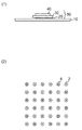
- FIG. 6A shows a side view of the multilayer printed circuit board 10 on which an integrated circuit (IC) 50 composed of the IC chip 40, the package substrate 30, and the ball 20 is mounted.
- IC integrated circuit
- FIG. 6 (1) the surface of the multilayer printed circuit board 10 is connected to the lower surface of the package substrate 30 through pads and balls 20.
- the power supply vias 2 and the ground vias 6 are arranged in a grid pattern. 6 (2), the induced electromotive forces generated in the multilayer printed board 10 by the vias cancel each other out, and the mutual inductance between the individual vias becomes small. Overall reliability and electrical properties are improved.
- the present invention provides a multilayer printed circuit board on which an integrated circuit (IC) is mounted, which suppresses the generation of induced electromotive force in the multilayer printed circuit board and eliminates noise countermeasure components such as a bypass capacitor, and also provides a lower surface of the multilayer printed circuit board. It is an object of the present invention to make it possible to arrange components on the bottom surface even when a case such as a bypass capacitor is required.
- IC integrated circuit
- a multilayer printed board according to the present invention is a multilayer printed board on which an integrated circuit is mounted, A plurality of power supply vias electrically connected to the power supply wiring; A plurality of ground vias electrically connected to the ground wiring; A plurality of power supply balls electrically connected to the power supply wiring of the integrated circuit; a plurality of power supply ball pads connected; and A plurality of ground balls electrically connected to the ground wiring of the integrated circuit, and a plurality of ground ball pads to be connected;
- the power supply vias and the ground vias are alternately arranged in the first direction, but are not alternately arranged in the second direction orthogonal to the first direction.
- the power supply ball pad and the ground ball pad are alternately arranged in at least one of the first direction and the two directions,
- the region where the power supply ball pad and the ground ball pad are provided is arranged on both sides in the second direction with respect to the region where the power supply via and the ground via are provided.
- the power supply vias and the ground vias are alternately arranged in the first direction, so that the generation of induced electromotive force in the multilayer printed board can be suppressed.
- the region where the power supply ball pad and the ground ball pad are provided is orthogonal to the first direction in which the power supply via and the ground via are alternately arranged with respect to the region where the power supply via and the ground via are provided. Since it is arranged on both sides in the second direction, it is possible to provide a region on the lower surface of the multilayer printed board on which a component such as a bypass capacitor is arranged.
- FIG. 6A is a side view of a general multilayer printed circuit board on which an integrated circuit (IC) is mounted.
- FIG. 6B is a plan view showing the arrangement of vias on the surface of a conventional multilayer printed board.
- FIG. 1A is a diagram showing the arrangement of vias and wirings on the surface of the multilayer printed circuit board according to the first embodiment of the present invention.
- the surface of the multilayer printed board 10 shown in FIG. 1A is a surface in contact with the ball 20 on the lower surface of the package board 30 as shown in FIG.
- a large number of power supply vias 2 and ground vias 6 are arranged on the multilayer printed board 10 shown in FIG.
- the power supply vias 2 and the ground vias 6 are alternately arranged in the horizontal direction (direction H) in FIG. However, they are not alternately arranged in the vertical direction (direction of V).
- a large number of power supply ball pads 12 and ground ball pads 16 are arranged on the surface of the multilayer printed board 10 shown in FIG.
- the power supply ball pads 12 and the ground ball pads 16 are alternately arranged in the vertical direction of FIG.
- the power supply via 2 and the power supply ball pad 12 are connected by a power supply wiring 22 on the surface of the multilayer printed board 10.
- the ground via 6 and the ground ball pad 16 are connected by a ground wiring 26.
- the power supply wiring 22 and the ground wiring 26 are alternately arranged.
- the ball 20 of the package substrate 30 is connected to the ball pads 12 and 16.
- FIG. 1B is a plan view for explaining only the arrangement of the power supply via 2 and the ground via 6 in FIG.
- the power supply vias 2 and the ground vias 6 are alternately arranged in the horizontal direction, but are not arranged alternately in the vertical direction.
- FIG. 1C shows only the arrangement of the power supply ball pad 12 and the ground ball pad 16 in FIG.
- the power supply ball pads 12 and the ground ball pads 16 are alternately arranged in the vertical direction and the horizontal direction.
- the power supply vias 2 and the ground vias 6 are alternately arranged in the horizontal direction, so that induced electromotive forces generated in the multilayer printed circuit board 10 due to the current flowing through the vias are mutually Be countered.
- IC Integrated Circuit
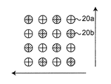
- FIG. 2 is a view showing the arrangement of balls (power supply balls 20a and ground balls 20b) on the lower surface of the integrated circuit (IC) 50 mounted on the multilayer printed circuit board 10 according to the first embodiment of the present invention. is there.
- the power supply balls 20a connected to the power supply ball pads 12 and the ground balls 20b connected to the ground ball pads 16 are alternately arranged.
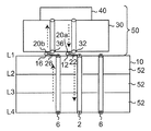
- FIG. 3 is a diagram schematically showing a partial cross section of the multilayer printed circuit board 10 and the package substrate 30 according to the first embodiment of the present invention.
- a multilayer printed circuit board 10 shown in FIG. 3 includes a plurality of conductor layers L1, L2, L3, and L4.
- a resin layer 52 is formed between the conductor layers L1, L2, L3, and L4.
- the second conductor layer L2 is a conductor layer (ground layer) connected to the ground, and is electrically connected to the ground via 6.
- the third conductor layer L3 is a conductor layer (power supply layer) connected to the power supply, and is electrically connected to the power supply via 2.
- FIG. 3 is an example of a four-layer through substrate, and a ground layer and a power supply layer are also examples. Therefore, the multilayer printed circuit board 10 may have a layer configuration other than four layers, and the ground layer and the power supply layer may be configured by any layer, or may be wired as a simple pattern.
- the ground via 6 of the multilayer printed board 10 is connected to the ground ball 20 b and the ground via 36 in the package substrate 30 via the ground wiring 26 and the ground ball pad 16.
- the power supply via 2 of the multilayer printed circuit board 10 is connected to the power supply ball 20 a in the package substrate 30 and the power supply via 32 in the package substrate through the power supply wiring 22 and the power supply ball pad 12.
- the power supply ball pads 12 and the ground ball pads 16 are alternately arranged in a predetermined direction.
- the LSI ground vias 36 connected to the balls are alternately arranged in a predetermined direction.
- the ground via 36 and the power supply via 32 of the package substrate 30 in FIG. 3 are shown as through vias, these may be built-up ones.
- the induced electromotive force generated in the multilayer printed circuit board 10 and the package substrate 30 is canceled by the arrangement of the vias in the multilayer printed circuit board 10 and the balls in the package circuit board 30, thereby reducing the mutual inductance. it can. As a result, the reliability and electrical characteristics of the entire system including the package substrate 30 and the multilayer printed circuit board 10 are improved.
- the region 13 in which the power supply ball pad 12 and the ground ball pad are provided is arranged on both sides in the vertical direction with respect to the region 3 in which the power supply via 2 and the ground via 6 are provided. That is, paying attention to the vertical direction in FIG. 1, the adjacent vias 2 and 6 are spaced apart so that at least two rows of ball pads 12 and 16 can be disposed. Therefore, in the vertical direction orthogonal to the horizontal direction in FIG. 1, an area is provided on the lower surface of the multilayer printed board 10 to the extent that components such as a bypass capacitor are arranged. Considering the ease of component placement on the lower surface of the multilayer printed circuit board 10, as shown in FIG.
- FIGS. 1 and 2 the power supply via 2, the ground via 6, the power supply ball pad 12, and the ground in the multilayer printed circuit board 10 according to the first embodiment of the present invention.
- the arrangement of the ball pads 16 for use and the arrangement of the balls 20 of the package substrate 30 are shown.
- the arrangement of the multilayer printed circuit board 10 and the package substrate 30 according to the first embodiment is not limited to that shown in FIGS. Examples of other arrangements will be described with reference to FIGS.
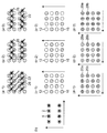
- FIG. 4 (a-1) shows the same arrangement as shown in FIG. 1 (a).
- This arrangement is based on a combination of the arrangement of the power supply via 2 and the ground via 6 shown in FIG. 4B and the arrangement of the power supply ball pad 12 and the ground ball pad 16 shown in FIG. 4C-1. realizable.
- FIG. 4D-1 is a diagram showing the arrangement of the power supply balls 20a and the ground balls 20b on the lower surface of the package substrate 30 mounted on the multilayer printed board 10 at this time.
- FIG. 4 (a-2) shows a first example of other arrangements.
- the arrangement shown in FIG. 4A-2 includes the arrangement of the power supply via 2 and the ground via 6 shown in FIG. 4B, and the power supply ball pad 12 and the ground ball shown in FIG. 4C-2.
- This can be realized by a combination with the arrangement of the pads 16. That is, regarding the arrangement of the ball pads, as shown in FIG. 4 (c-2), the same type of ball pads 12, 16 are arranged in the horizontal direction, and in the vertical direction, the power supply ball pad 12 and the ground ball pad are arranged. 16 are alternately arranged.
- FIG. 4D-2 is a diagram showing the arrangement of the power supply balls 20a and the ground balls 20b on the lower surface of the package substrate 30 mounted on the multilayer printed board 10 at this time.
- FIG. 4 (a-3) shows a second example of other arrangements.
- the arrangement shown in FIG. 4A-3 includes the arrangement of the power supply via 2 and the ground via 6 shown in FIG. 4B, and the power supply ball pad 12 and the ground ball shown in FIG. 4C-3.
- This can be realized by a combination with the arrangement of the pads 16. That is, regarding the arrangement of the ball pads, as shown in FIG. 4 (c-3), two ball pads 12 and 16 of the same type are arranged in the horizontal direction, and in the vertical direction, the power supply ball pad 12 and the ground are arranged.
- the ball pads 16 for use are arranged alternately.
- FIG. 4D-3 is a diagram showing the arrangement of the power supply balls 20a and the ground balls 20b on the lower surface of the package substrate 30 mounted on the multilayer printed board 10 at this time.
- FIG. 5 (a-4) shows a third example of other arrangements.
- the arrangement shown in FIG. 5 (a-4) includes the arrangement of the power supply via 2 and the ground via 6 shown in FIG. 5 (b), and the power supply ball pad 12 and the ground ball shown in FIG. 5 (c-4). This can be realized by a combination with the arrangement of the pads 16.
- the arrangement of the power supply via 2 and the ground via 6 shown in FIG. 5B is the same as the arrangement of the power supply via 2 and the ground via 6 shown in FIG.
- FIG. 5C-4 is a diagram showing the arrangement of the power supply balls 20a and the ground balls 20b on the lower surface of the package substrate 30 mounted on the multilayer printed board 10 at this time.
- FIG. 5 (a-5) shows a fourth example of other arrangements.
- the arrangement shown in FIG. 5 (a-5) includes the arrangement of the power supply via 2 and the ground via 6 shown in FIG. 5 (b), and the power supply ball pad 12 and the ground ball shown in FIG. 5 (c-5). This can be realized by a combination with the arrangement of the pads 16.
- FIG. 5C-5 is a diagram showing the arrangement of the power supply balls 20a and the ground balls 20b on the lower surface of the package substrate 30 mounted on the multilayer printed board 10 at this time.
- the multilayer printed circuit board according to the first embodiment is a multilayer printed circuit board 10 on which an integrated circuit (IC) 50 is mounted via a ball pad arranged on the surface.
- the multilayer printed circuit board 10 is electrically connected to a plurality of power supply vias 2 electrically connected to the power supply wiring, a plurality of ground vias 6 electrically connected to the ground wiring, and a power supply wiring of the package substrate 30.
- a plurality of power supply ball pads 12 connected to the power supply balls 20 a and a plurality of ground ball pads 16 connected to the ground balls 20 b electrically connected to the ground wiring of the package substrate 30 are provided.
- the power supply vias 2 and the ground vias 6 are alternately arranged in the first direction (H direction), but are alternately arranged in the second direction (V direction) orthogonal to the first direction. Not placed in.
- the power supply ball pad 12 and the ground ball pad 16 are alternately arranged in at least one of the first direction and the second direction. Further, the region 13 where the power supply ball pad and the ground ball pad are provided is arranged on both sides in the second direction with respect to the region 3 where the power supply via 2 and the ground via 6 are provided.
- the integrated circuit (IC) 50 mounted on the multilayer printed circuit board 10 is connected to the multilayer printed circuit board 10 through the plurality of power supply ball pads 12.
- a ball 20 a and a plurality of ground balls 20 b electrically connected to the multilayer printed circuit board 10 through a plurality of ground ball pads 16 of the multilayer printed circuit board 10 are provided.
- the power supply balls 20a and the ground balls 20b are alternately arranged in the direction in which the power supply ball pads 12 and the ground ball pads 16 are alternately arranged on the multilayer printed circuit board 10. Is done.
- the adjacent vias 2 and 6 are disposed so as to dispose at least two rows of ball pads 12 and 16, and Since the power supply vias 2 and the ground vias 6 are not alternately arranged, it is possible to provide an area on the lower surface of the multilayer printed circuit board 10 for arranging components such as a bypass capacitor. Further, in such a multilayer printed circuit board 10, the power supply vias 2 and the ground vias 6 are alternately arranged in the first direction (H direction), so that an induced electromotive force is generated in the multilayer printed circuit board 10. It can be suppressed. Therefore, the reliability and electrical characteristics of the package substrate 30 are improved.
- the power supply ball pad 12, the power supply ball 20a, and the ground ball pad 16 are provided in at least one of the first direction and the second direction. Since the ground balls 20b are alternately arranged, not only the induced electromotive force in the multilayer printed board 10 but also the induced electromotive force in the package substrate 30 can be suppressed. Therefore, the reliability and electrical characteristics of the entire system including the package substrate 30 and the multilayer printed circuit board 10 are improved.
- the present invention can be used in a multilayer printed board on which an integrated circuit (IC) of BGA (Ball Grid Array) type is mounted.
- IC integrated circuit
- BGA Ball Grid Array
Landscapes
- Engineering & Computer Science (AREA)
- Microelectronics & Electronic Packaging (AREA)
- Physics & Mathematics (AREA)
- Electromagnetism (AREA)
- Production Of Multi-Layered Print Wiring Board (AREA)
- Wire Bonding (AREA)
Abstract
Description
電源配線と電気的に接続する複数の電源用ビアと、
グランド配線と電気的に接続する複数のグランド用ビアと、
前記集積回路の電源配線と電気的に接続する複数の電源用ボールと、接続する、複数の電源用ボールパッドと、及び、
前記集積回路のグランド配線と電気的に接続する複数のグランド用ボールと、接続する、複数のグランド用ボールパッドとを備え、
前記電源用ビアと前記グランド用ビアは、第1の方向において交互に配置されるが、前記第1の方向と直交する第2の方向においては交互に配置されず、
前記電源用ボールパッドと前記グランド用ボールパッドは、前記第1の方向と前記2の方向のうちの少なくとも一つの方向において、交互に配置され、
前記電源用ボールパッドと前記グランド用ボールパッドを設ける領域は、前記電源用ビアと前記グランド用ビアを設ける領域に対して、前記第2の方向において両隣に配置される。
1.構成
1.1.多層プリント基板の構成
図1(a)は、本発明の第1の実施形態に係る多層プリント基板の表面でのビア及び配線の配置を示した図である。図1(a)に示す多層プリント基板10の表面は、図6(1)に示すような、パッケージ基板30の下面のボール20と接する面である。
多層プリント基板10上にパッケージ基板30を実装する場合、多層プリント基板10の電源用ボールパッド12は、パッケージ基板30の電源用ボール20aに直接接続し、多層プリント基板10のグランド用ボールパッド16は、パッケージ基板30のグランド用ボール20bに直接接続する。つまり、多層プリント基板10とパッケージ基板30との間において、多層プリント基板10の電源用ボールパッド12の位置は、パッケージ基板30の電源用ボール20aの位置に対応し、多層プリント基板10のグランド用ボールパッド16の位置は、パッケージ基板30のグランド用ボール20bの位置に対応する。
図3は、本発明の第1の実施形態に係る多層プリント基板10とパッケージ基板30の一部断面を模式的に表した図である。図3に示す多層プリント基板10は、複数の導体層L1、L2、L3、L4により構成される。各導体層L1、L2、L3、L4の間には樹脂層52が形成されている。ここで、2番目の導体層L2は、グランドに接続する導体層(グランド層)であり、グランド用ビア6と電気的に接続する。3番目の導体層L3は、電源に接続する導体層(電源層)であり、電源用ビア2と電気的に接続する。よって、グランド用ビア6と電源用ビア2とを所定の方向に関して交互に配置することで、夫々のビアを流れる電流により発生する誘導起電力が、相互に打ち消される。なお、図3は4層貫通基板の一例であり、グランド層や電源層も一例である。よって多層プリント基板10の層構成は4層以外のものでも構わず、グランド層と電源層もどの層で構成をしても構わないし、単なるパターンとして配線しても構わない。
図1及び図2にて、本発明の第1の実施形態に係る多層プリント基板10における電源用ビア2、グランド用ビア6、電源用ボールパッド12、及びグランド用ボールパッド16の配置、並びに、パッケージ基板30のボール20の配置を示した。第1の実施形態に係る多層プリント基板10及びパッケージ基板30における配置は、図1及び図2に示すものに限定されない。その他の配置の例を、図4及び図5を用いて説明する。
図4(a-2)にその他の配置の第1の例を示す。図4(a-2)に示す配置は、図4(b)に示す電源用ビア2とグランド用ビア6の配置と、図4(c-2)に示す電源用ボールパッド12とグランド用ボールパッド16の配置との組み合わせにより実現できる。すなわち、ボールパッドの配置に関して、図4(c-2)に示すように、横方向に同じ種類のボールパッド12、16を配置し、縦方向においては、電源用ボールパッド12とグランド用ボールパッド16とを交互に配置している。図4(d-2)は、このとき多層プリント基板10に実装されるパッケージ基板30の下面における電源用ボール20a及びグランド用ボール20bの配置を示した図である。
図4(a-3)にその他の配置の第2の例を示す。図4(a-3)に示す配置は、図4(b)に示す電源用ビア2とグランド用ビア6の配置と、図4(c-3)に示す電源用ボールパッド12とグランド用ボールパッド16の配置との組み合わせにより実現できる。すなわち、ボールパッドの配置に関して、図4(c-3)に示すように、横方向に2つずつ同じ種類のボールパッド12、16を配置し、縦方向においては、電源用ボールパッド12とグランド用ボールパッド16とを交互に配置している。図4(d-3)は、このとき多層プリント基板10に実装されるパッケージ基板30の下面における電源用ボール20a及びグランド用ボール20bの配置を示した図である。
図5(a-4)にその他の配置の第3の例を示す。図5(a-4)に示す配置は、図5(b)に示す電源用ビア2とグランド用ビア6の配置と、図5(c-4)に示す電源用ボールパッド12とグランド用ボールパッド16の配置との組み合わせにより実現できる。図5(b)に示す電源用ビア2とグランド用ビア6の配置は、図4(b)に示す電源用ビア2とグランド用ビア6の配置と同一のものである。
図5(a-5)にその他の配置の第4の例を示す。図5(a-5)に示す配置は、図5(b)に示す電源用ビア2とグランド用ビア6の配置と、図5(c-5)に示す電源用ボールパッド12とグランド用ボールパッド16の配置との組み合わせにより実現できる。
第1の実施形態に係る多層プリント基板は、表面に配置されたボールパッドを介して、集積回路(IC)50を実装する多層プリント基板10である。多層プリント基板10は、電源配線と電気的に接続する複数の電源用ビア2と、グランド配線と電気的に接続する複数のグランド用ビア6と、パッケージ基板30の電源配線と電気的に接続する電源用ボール20aと接続する、複数の電源用ボールパッド12と、及び、パッケージ基板30のグランド配線と電気的に接続するグランド用ボール20bと接続する、複数のグランド用ボールパッド16とを備える。ここで、電源用ビア2とグランド用ビア6は、第1の方向(Hの方向)において交互に配置されるが、第1の方向と直交する第2の方向(Vの方向)においては交互に配置されない。電源用ボールパッド12とグランド用ボールパッド16は、第1の方向と第2の方向のうちの少なくとも一つの方向において、交互に配置される。更に、電源用ボールパッドとグランド用ボールパッドを設ける領域13は、電源用ビア2とグランド用ビア6を設ける領域3に対して、第2の方向の両隣に配置される。
Claims (3)
- 集積回路を実装する多層プリント基板であって、
電源配線と電気的に接続する複数の電源用ビアと、
グランド配線と電気的に接続する複数のグランド用ビアと、
前記集積回路の電源配線と電気的に接続する電源用ボールと接続する、複数の電源用ボールパッドと、及び、
前記集積回路のグランド配線と電気的に接続するグランド用ボールと接続する、複数のグランド用ボールパッドとを備え、
前記電源用ビアと前記グランド用ビアは、第1の方向において交互に配置されるが、前記第1の方向と直交する第2の方向においては交互に配置されず、
前記電源用ボールパッドと前記グランド用ボールパッドは、前記第1の方向と前記第2の方向のうちの少なくとも一つの方向において、交互に配置され、
前記電源用ボールパッドと前記グランド用ボールパッドを設ける領域は、前記電源用ビアと前記グランド用ビアを設ける領域に対して、前記第2の方向において両隣に配置されることを特徴とする
多層プリント基板。 - 請求項1に記載の多層プリント基板上に実装される集積回路であって、
前記多層プリント基板の複数の前記電源用ボールパッドと電気的に接続する複数の電源用ボールと、
前記多層プリント基板の複数の前記グランド用ボールパッドと電気的に接続する複数のグランド用ボールとを備え、
前記電源用ボールと前記グランド用ボールは、前記多層プリント基板における前記電源用ボールパッドと前記グランド用ボールパッドが交互に配置される前記少なくとも一つの方向において、交互に配置されることを特徴とする
集積回路。 - 請求項2に記載の集積回路を実装した請求項1に記載の多層プリント基板。
Priority Applications (4)
| Application Number | Priority Date | Filing Date | Title |
|---|---|---|---|
| PCT/JP2012/000522 WO2013111194A1 (ja) | 2012-01-27 | 2012-01-27 | 多層プリント基板 |
| EP12866538.7A EP2808890A4 (en) | 2012-01-27 | 2012-01-27 | MULTILAYER CONDUCTOR PLATE |
| US14/374,198 US9549459B2 (en) | 2012-01-27 | 2012-01-27 | Multilayer printed circuit board |
| JP2013554996A JP5919558B2 (ja) | 2012-01-27 | 2012-01-27 | 多層プリント基板 |
Applications Claiming Priority (1)
| Application Number | Priority Date | Filing Date | Title |
|---|---|---|---|
| PCT/JP2012/000522 WO2013111194A1 (ja) | 2012-01-27 | 2012-01-27 | 多層プリント基板 |
Publications (1)
| Publication Number | Publication Date |
|---|---|
| WO2013111194A1 true WO2013111194A1 (ja) | 2013-08-01 |
Family
ID=48872974
Family Applications (1)
| Application Number | Title | Priority Date | Filing Date |
|---|---|---|---|
| PCT/JP2012/000522 Ceased WO2013111194A1 (ja) | 2012-01-27 | 2012-01-27 | 多層プリント基板 |
Country Status (4)
| Country | Link |
|---|---|
| US (1) | US9549459B2 (ja) |
| EP (1) | EP2808890A4 (ja) |
| JP (1) | JP5919558B2 (ja) |
| WO (1) | WO2013111194A1 (ja) |
Cited By (3)
| Publication number | Priority date | Publication date | Assignee | Title |
|---|---|---|---|---|
| US10306761B2 (en) | 2016-12-13 | 2019-05-28 | Canon Kabushiki Kaisha | Printed wiring board, printed circuit board, and electronic apparatus |
| JPWO2019065494A1 (ja) * | 2017-09-29 | 2020-06-18 | アイシン・エィ・ダブリュ株式会社 | 回路基板、回路基板の設計方法、及び半導体装置 |
| JP2025061223A (ja) * | 2020-11-26 | 2025-04-10 | 三菱電機株式会社 | プリント配線板 |
Families Citing this family (11)
| Publication number | Priority date | Publication date | Assignee | Title |
|---|---|---|---|---|
| US9609749B2 (en) * | 2014-11-14 | 2017-03-28 | Mediatek Inc. | Printed circuit board having power/ground ball pad array |
| CN105374694B (zh) * | 2015-12-04 | 2020-09-01 | 上海兆芯集成电路有限公司 | 芯片装置及其凸块配置方法 |
| TWI640229B (zh) * | 2017-04-14 | 2018-11-01 | 和碩聯合科技股份有限公司 | 電源信號傳遞結構及其設計方法 |
| TWI686112B (zh) * | 2017-06-22 | 2020-02-21 | 上海兆芯集成電路有限公司 | 印刷電路板和半導體封裝結構 |
| TWI686113B (zh) * | 2017-06-22 | 2020-02-21 | 上海兆芯集成電路有限公司 | 印刷電路板和半導體封裝結構 |
| TWI686111B (zh) * | 2017-06-22 | 2020-02-21 | 上海兆芯集成電路有限公司 | 印刷電路板和半導體封裝結構 |
| TWI698157B (zh) | 2019-01-02 | 2020-07-01 | 瑞昱半導體股份有限公司 | 主控元件及電路基板 |
| CN113096933B (zh) | 2020-01-08 | 2022-04-22 | 台达电子企业管理(上海)有限公司 | 多相耦合电感、多相耦合电感阵列及两相反耦合电感 |
| US12342450B2 (en) * | 2020-01-08 | 2025-06-24 | Delta Electronics (Shanghai) Co., Ltd | Power supply apparatus, load and electronic device |
| CN113098234B (zh) | 2020-01-08 | 2022-11-01 | 台达电子企业管理(上海)有限公司 | 供电系统 |
| US12610453B2 (en) | 2020-01-08 | 2026-04-21 | Delta Electronics (Shanghai) Co., Ltd. | Vertical power supply system and manufacturing method of connection board |
Citations (7)
| Publication number | Priority date | Publication date | Assignee | Title |
|---|---|---|---|---|
| JPH10303562A (ja) * | 1997-04-30 | 1998-11-13 | Toshiba Corp | プリント配線板 |
| JP2001148448A (ja) * | 1999-11-19 | 2001-05-29 | Kyocera Corp | 集積回路素子搭載用基板および集積回路装置 |
| JP2003332377A (ja) * | 2002-05-07 | 2003-11-21 | Toshiba Corp | フリップチップボンディングのための有機基板 |
| JP2006114777A (ja) | 2004-10-15 | 2006-04-27 | Toshiba Corp | プリント配線基板及びこの基板を搭載する情報処理装置 |
| JP2006128687A (ja) * | 2004-10-26 | 2006-05-18 | Toshiba Corp | 半導体パッケージと共に使用するための基板層及びその形成方法 |
| US20070034405A1 (en) | 2005-08-10 | 2007-02-15 | Alcatel | Using rows/columns of micro-vias to create PCB routing channels in BGA interconnect grid (micro-via channels) |
| JP2010283396A (ja) | 2003-04-07 | 2010-12-16 | Ibiden Co Ltd | 多層プリント配線板 |
Family Cites Families (9)
| Publication number | Priority date | Publication date | Assignee | Title |
|---|---|---|---|---|
| US5272600A (en) * | 1992-09-02 | 1993-12-21 | Microelectronics And Computer Technology Corporation | Electrical interconnect device with interwoven power and ground lines and capacitive vias |
| US5544018A (en) * | 1994-04-13 | 1996-08-06 | Microelectronics And Computer Technology Corporation | Electrical interconnect device with customizeable surface layer and interwoven signal lines |
| JP3178399B2 (ja) * | 1997-12-04 | 2001-06-18 | 日本電気株式会社 | 半導体集積回路、その素子配置方法およびその製造方法 |
| US6198635B1 (en) * | 1999-05-18 | 2001-03-06 | Vsli Technology, Inc. | Interconnect layout pattern for integrated circuit packages and the like |
| US20040003941A1 (en) * | 2000-06-19 | 2004-01-08 | Duxbury Guy A. | Technique for electrically interconnecting electrical signals between an electronic component and a multilayer signal routing device |
| US7005736B2 (en) * | 2002-09-30 | 2006-02-28 | Intel Corporation | Semiconductor device power interconnect striping |
| KR101218011B1 (ko) * | 2003-11-08 | 2013-01-02 | 스태츠 칩팩, 엘티디. | 플립 칩 인터커넥션 패드 레이아웃 반도체 패키지 및 그 생산 방법 |
| US6992374B1 (en) * | 2004-06-14 | 2006-01-31 | Cisco Technology, Inc. | Techniques for manufacturing a circuit board with an improved layout for decoupling capacitors |
| US8350375B2 (en) * | 2008-05-15 | 2013-01-08 | Lsi Logic Corporation | Flipchip bump patterns for efficient I-mesh power distribution schemes |
-
2012
- 2012-01-27 EP EP12866538.7A patent/EP2808890A4/en not_active Withdrawn
- 2012-01-27 US US14/374,198 patent/US9549459B2/en not_active Expired - Fee Related
- 2012-01-27 JP JP2013554996A patent/JP5919558B2/ja active Active
- 2012-01-27 WO PCT/JP2012/000522 patent/WO2013111194A1/ja not_active Ceased
Patent Citations (7)
| Publication number | Priority date | Publication date | Assignee | Title |
|---|---|---|---|---|
| JPH10303562A (ja) * | 1997-04-30 | 1998-11-13 | Toshiba Corp | プリント配線板 |
| JP2001148448A (ja) * | 1999-11-19 | 2001-05-29 | Kyocera Corp | 集積回路素子搭載用基板および集積回路装置 |
| JP2003332377A (ja) * | 2002-05-07 | 2003-11-21 | Toshiba Corp | フリップチップボンディングのための有機基板 |
| JP2010283396A (ja) | 2003-04-07 | 2010-12-16 | Ibiden Co Ltd | 多層プリント配線板 |
| JP2006114777A (ja) | 2004-10-15 | 2006-04-27 | Toshiba Corp | プリント配線基板及びこの基板を搭載する情報処理装置 |
| JP2006128687A (ja) * | 2004-10-26 | 2006-05-18 | Toshiba Corp | 半導体パッケージと共に使用するための基板層及びその形成方法 |
| US20070034405A1 (en) | 2005-08-10 | 2007-02-15 | Alcatel | Using rows/columns of micro-vias to create PCB routing channels in BGA interconnect grid (micro-via channels) |
Non-Patent Citations (1)
| Title |
|---|
| See also references of EP2808890A4 |
Cited By (3)
| Publication number | Priority date | Publication date | Assignee | Title |
|---|---|---|---|---|
| US10306761B2 (en) | 2016-12-13 | 2019-05-28 | Canon Kabushiki Kaisha | Printed wiring board, printed circuit board, and electronic apparatus |
| JPWO2019065494A1 (ja) * | 2017-09-29 | 2020-06-18 | アイシン・エィ・ダブリュ株式会社 | 回路基板、回路基板の設計方法、及び半導体装置 |
| JP2025061223A (ja) * | 2020-11-26 | 2025-04-10 | 三菱電機株式会社 | プリント配線板 |
Also Published As
| Publication number | Publication date |
|---|---|
| JP5919558B2 (ja) | 2016-05-18 |
| US9549459B2 (en) | 2017-01-17 |
| EP2808890A1 (en) | 2014-12-03 |
| EP2808890A4 (en) | 2015-08-19 |
| US20140334121A1 (en) | 2014-11-13 |
| JPWO2013111194A1 (ja) | 2015-05-11 |
Similar Documents
| Publication | Publication Date | Title |
|---|---|---|
| JP5919558B2 (ja) | 多層プリント基板 | |
| JP2013033988A (ja) | 回路基板およびこれを利用した半導体パッケージ | |
| US20120241208A1 (en) | Signal routing Optimized IC package ball/pad layout | |
| US7541683B2 (en) | Semiconductor integrated circuit device | |
| JP6671551B1 (ja) | 多層プリント基板 | |
| US8093708B2 (en) | Semiconductor package having non-uniform contact arrangement | |
| US7161812B1 (en) | System for arraying surface mount grid array contact pads to optimize trace escape routing for a printed circuit board | |
| JP5213034B2 (ja) | Bgaパッケージ | |
| CN103889145A (zh) | 线路板及电子总成 | |
| JP7621099B2 (ja) | プリント配線板 | |
| US8125794B2 (en) | Multilayer printed wiring board and electronic device using the same | |
| JP2010153831A5 (ja) | 配線基板および半導体装置 | |
| US8631706B2 (en) | Noise suppressor for semiconductor packages | |
| US20080251286A1 (en) | Method For Increasing a Routing Density For a Circuit Board and Such a Circuit Board | |
| JP6469441B2 (ja) | 多層配線板 | |
| JP5691651B2 (ja) | 集積回路放熱装置及び電子装置 | |
| JP2007335618A (ja) | プリント回路基板 | |
| US8912656B2 (en) | Integrated circuit package and physical layer interface arrangement | |
| JP2011071322A (ja) | 電子装置 | |
| JP5691931B2 (ja) | 電子装置 | |
| JP4876655B2 (ja) | 実装構造体および電子機器 | |
| JP4382774B2 (ja) | 半導体パッケージ、ボード、電子機器、及び半導体パッケージとプリント板の接続方法 | |
| CN1971897A (zh) | 球格阵列布线架构 | |
| KR20100047203A (ko) | 반도체 패키지 | |
| JP2005005601A (ja) | 印刷回路配線板の配線レイアウト構造 |
Legal Events
| Date | Code | Title | Description |
|---|---|---|---|
| 121 | Ep: the epo has been informed by wipo that ep was designated in this application |
Ref document number: 12866538 Country of ref document: EP Kind code of ref document: A1 |
|
| ENP | Entry into the national phase |
Ref document number: 2013554996 Country of ref document: JP Kind code of ref document: A |
|
| WWE | Wipo information: entry into national phase |
Ref document number: 2012866538 Country of ref document: EP |
|
| WWE | Wipo information: entry into national phase |
Ref document number: 14374198 Country of ref document: US |
|
| NENP | Non-entry into the national phase |
Ref country code: DE |