WO2013111261A1 - 電力変換装置及びその製造方法 - Google Patents
電力変換装置及びその製造方法 Download PDFInfo
- Publication number
- WO2013111261A1 WO2013111261A1 PCT/JP2012/051320 JP2012051320W WO2013111261A1 WO 2013111261 A1 WO2013111261 A1 WO 2013111261A1 JP 2012051320 W JP2012051320 W JP 2012051320W WO 2013111261 A1 WO2013111261 A1 WO 2013111261A1
- Authority
- WO
- WIPO (PCT)
- Prior art keywords
- unit
- semiconductor
- spring
- plate
- frame
- Prior art date
- Legal status (The legal status is an assumption and is not a legal conclusion. Google has not performed a legal analysis and makes no representation as to the accuracy of the status listed.)
- Ceased
Links
Images




Classifications
-
- H—ELECTRICITY
- H02—GENERATION; CONVERSION OR DISTRIBUTION OF ELECTRIC POWER
- H02M—APPARATUS FOR CONVERSION BETWEEN AC AND AC, BETWEEN AC AND DC, OR BETWEEN DC AND DC, AND FOR USE WITH MAINS OR SIMILAR POWER SUPPLY SYSTEMS; CONVERSION OF DC OR AC INPUT POWER INTO SURGE OUTPUT POWER; CONTROL OR REGULATION THEREOF
- H02M7/00—Conversion of AC power input into DC power output; Conversion of DC power input into AC power output
- H02M7/003—Constructional details, e.g. physical layout, assembly, wiring or busbar connections
-
- H—ELECTRICITY
- H10—SEMICONDUCTOR DEVICES; ELECTRIC SOLID-STATE DEVICES NOT OTHERWISE PROVIDED FOR
- H10W—GENERIC PACKAGES, INTERCONNECTIONS, CONNECTORS OR OTHER CONSTRUCTIONAL DETAILS OF DEVICES COVERED BY CLASS H10
- H10W40/00—Arrangements for thermal protection or thermal control
- H10W40/20—Arrangements for cooling
- H10W40/22—Arrangements for cooling characterised by their shape, e.g. having conical or cylindrical projections
-
- H—ELECTRICITY
- H10—SEMICONDUCTOR DEVICES; ELECTRIC SOLID-STATE DEVICES NOT OTHERWISE PROVIDED FOR
- H10W—GENERIC PACKAGES, INTERCONNECTIONS, CONNECTORS OR OTHER CONSTRUCTIONAL DETAILS OF DEVICES COVERED BY CLASS H10
- H10W40/00—Arrangements for thermal protection or thermal control
- H10W40/60—Securing means for detachable heating or cooling arrangements, e.g. clamps
-
- H—ELECTRICITY
- H10—SEMICONDUCTOR DEVICES; ELECTRIC SOLID-STATE DEVICES NOT OTHERWISE PROVIDED FOR
- H10W—GENERIC PACKAGES, INTERCONNECTIONS, CONNECTORS OR OTHER CONSTRUCTIONAL DETAILS OF DEVICES COVERED BY CLASS H10
- H10W72/00—Interconnections or connectors in packages
- H10W72/071—Connecting or disconnecting
Definitions
- the technology disclosed in this specification relates to a power conversion device such as an inverter or a converter and a manufacturing method thereof.
- a structure in which semiconductor elements having a large heat generation such as IGBTs are integrated separately from other circuits and cooled intensively may be employed.
- a semiconductor stacked unit is known in which flat semiconductor modules containing semiconductor elements and flat coolers are alternately stacked (for example, Patent Document 1 to Patent Document 3).
- the semiconductor stacked unit is attached to the frame in a state where pressure is applied in the stacking direction so that heat is transferred from the semiconductor module to the cooler well.
- the frame is a structure that supports the semiconductor module, and may typically be a case of a power converter.
- a spring is inserted between one end of the semiconductor module in the stacking direction and a wall or a column provided on the frame.
- Patent Documents 1 to 3 disclose techniques for improving the efficiency of inserting a compressed spring between a frame wall or a column and a semiconductor module.
- Patent Document 1 discloses a technique of inserting a clip between a wall of a frame and a semiconductor module after compressing a clip-shaped leaf spring.
- Each of the techniques of Patent Document 2 and Patent Document 3 employs a spring unit in which a coil spring is sandwiched between two plates.
- the technology disclosed in Patent Document 2 is as follows. A spring unit is inserted from a slit provided in the wall of the frame, and the spring unit is compressed while pressing the front plate against the semiconductor lamination unit. When the rear plate passes through the slit, the rear plate is rotated 90 degrees. When the force to push the rear plate is loosened, both ends of the rear plate are caught on both sides of the slit, the spring unit applies pressure to the semiconductor multilayer unit, and the semiconductor multilayer unit is fixed.
- Patent Document 3 The technology disclosed in Patent Document 3 is as follows. With the spring unit compressed, a bolt is inserted from the rear plate, and the bolt is fixed to a screw hole provided on the back surface of the front plate. Thus, a spring unit maintained in a compressed state is obtained. A spring unit maintained in a compressed state is placed between the frame wall and the semiconductor lamination unit. The plate on the rear side of the spring unit is fixed to the frame. Then remove the bolts. When the bolt is removed, the spring is released, the spring unit applies a load to the semiconductor multilayer unit, and the semiconductor multilayer unit is fixed.
- the spring unit facilitates the assembly work of the semiconductor laminated unit, but there is room for improvement in the techniques of Patent Documents 2 and 3.
- the plate on the rear side of the spring unit is rotated while pressing the spring unit against the semiconductor laminated unit, so that a torsional force is applied to the semiconductor laminated unit and the rear plate is rotated.
- the pressure applied to the semiconductor laminated unit becomes non-uniform during and after compression of the spring unit. If the pressure applied to the semiconductor laminated unit is not uniform, the adhesion between the cooler and the semiconductor module may be reduced.
- the power conversion device includes a semiconductor laminated unit, a frame for attaching the semiconductor laminated unit, and a spring unit.
- the semiconductor stacked unit is a structure in which flat semiconductor modules containing semiconductor elements and flat coolers are alternately stacked. Opposed walls or pillars are provided on the frame, and a semiconductor laminated unit is fixed between the walls or pillars using a spring unit.
- the spring unit is mainly composed of first and second plates and a spring sandwiched between them.
- the first plate is a plate that comes into contact with the end surface of the semiconductor multilayer unit, and is provided with a recess so as to have a gap between the first plate and the end surface of the semiconductor multilayer unit.
- a 2nd plate is a plate contact
- the semiconductor stacked unit is placed between opposing walls or columns of the frame, and a spring unit is inserted between one end of the semiconductor stacked unit in the stacking direction and the wall or column provided on the frame.
- the semiconductor laminated unit is fixed while being pressed by a spring unit.
- the frame may be a case for housing the semiconductor multilayer unit.
- the spring is preferably a coil spring, but is not limited thereto.
- the frame may be provided with opposing walls and pillars, and the semiconductor stacked unit may be fixed between the walls and the pillars.
- the above power converter is assembled by the following process.
- a spring pin is compressed by pushing a lock pin having a hook at the tip into the through path from the second plate side.
- the lock pin has a flange (stopper) in the middle, and the flange pushes the second plate.
- a hook of the lock pin is hooked on the edge of the through hole opening of the first plate to hold the spring unit in a compressed state. That is, the spring unit is compressed between the flange of the lock pin and the hook.
- the semiconductor laminated unit is placed on the frame, and a spring unit held in a compressed state is placed between the frame wall or support and the end face of the semiconductor laminated unit.
- the lock pin is removed to release the spring unit, and pressure is applied to the semiconductor multilayer unit to fix the semiconductor multilayer unit.
- the spring unit having a through passage opened at the bottom of the depression of the first plate improves the assemblability of the power conversion device.
- the lock pin passed from the second plate side compresses the spring, and the hook at the tip engages the first plate. Lock pins make the spring unit easily compressed.
- the tip of the lock pin including the hook fits in the recess of the first plate. Therefore, the first plate can be in contact with the end surface of the semiconductor multilayer unit without the front end of the lock pin interfering.
- the lock pin is removed, the first plate uniformly applies pressure to the semiconductor stacked unit.
- the lock pin having a hook at the tip does not require a screw hole and does not generate dust. The above-described technique improves the assemblability of the power conversion device.
- the novel power conversion device disclosed in this specification is a device including a stacked semiconductor stacked unit, for example, an inverter that supplies power to a motor.
- a spring unit that supports a semiconductor stacked unit while applying pressure can be easily attached without generating dust. Details of the technology disclosed in this specification and further improvements will be described in the embodiments of the present invention.
- the power converter of an embodiment is an inverter that supplies AC power to a motor.
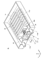
- FIG. 1 is a perspective view of the inverter 2.
- the inverter 2 includes a semiconductor laminated unit 20 in which power semiconductor elements such as IGBTs and diodes used in a switching circuit are integrated, a circuit for generating PWM for driving the power semiconductor elements, and a circuit for smoothing current. However, the illustration and description thereof are omitted.
- the inverter 2 uses a large number of power semiconductor elements.
- a large number of power semiconductor elements are packaged in flat resin molds. Each package is referred to as a semiconductor module 22.
- the semiconductor lamination unit 20 has a structure in which semiconductor modules 22 and flat plate coolers 21 are alternately laminated. In the semiconductor laminated unit 20 of FIG. 1, six semiconductor modules 22 and seven coolers 21 are alternately laminated. Grease is applied to the contact surface between the semiconductor module 22 and the cooler 21.
- the coolers 21 are connected to each other by pipes.
- the refrigerant supplied from the supply pipe 24 passes through each cooler 21 and is discharged from the discharge pipe 23.
- Each semiconductor module 22 is efficiently cooled from both sides.
- the semiconductor laminated unit 20 is a laminated structure, it is excellent in compactness.
- the semiconductor laminated unit 20 is fixed to the frame 12.
- the frame 12 is further housed in a case (not shown) of the inverter 2.
- the semiconductor stacked unit 20 is fixed between the opposing wall 14 provided on the frame 12 and the support column 13.
- a spring unit 6 is used to fix the semiconductor laminated unit 20.
- the spring unit 6 is inserted between one end face 20 a of the semiconductor multilayer unit 20 and the support column 13 of the frame 12, and applies pressure in the stacking direction to the semiconductor multilayer unit 20.
- grease is applied to the contact surface between the semiconductor module 22 and the cooler 21.
- the degree of adhesion between the semiconductor module 22 and the cooler 21 is increased, and the thermal conductivity from the semiconductor module 22 to the cooler 21 is improved. That is, the cooling efficiency is improved by applying pressure in the stacking direction to the semiconductor stacking unit 20.
- the inverter 2 is characterized by a spring unit 6.
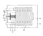
- FIG. 2 shows a plan view of the inverter 2
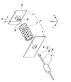
- FIG. 3 shows an exploded perspective view of the spring unit 6.
- the spring unit 6 is drawn in a cross section cut along the XY plane in the drawing. The same applies to the plan views of FIGS.
- the spring unit 6 includes two plates (the first plate 5 and the second plate 4) and a coil spring 3 sandwiched between the two plates.
- the first plate 5 comes into contact with one end face 20 a of the semiconductor stacked unit 20, and the second plate 4 comes into contact with the column 13 fixed to the frame 12.
- a recess 5 b is provided so as to have a gap with the end surface 20 a of the semiconductor multilayer unit 20.
- a diameter D (see FIG. 3) of the protrusion 5d corresponding to the recess 5b when viewed from the back surface of the first plate 5 is a size to which the coil spring 3 is fitted.
- An elliptical hole 5a is provided on the bottom surface of the recess 5b.
- the second plate 4 is provided with a central hole 4a.
- the spring unit 6 is formed with a through-passage 9 that passes from the central hole 4a of the second plate 4 through the inside of the coil spring 3 to the elliptical hole 5a of the first plate 5 (see FIGS. 2 and 3).
- the elliptical hole 5 a of the first plate 5 corresponds to one opening of the through passage 9, and the central hole 4 a of the second plate 3 corresponds to the other opening of the through hole 9.
- the through passage 9 is provided for passing the lock pin 30 having the hook 33 at the tip.
- the lock pin 30 is a tool that holds the spring unit 6 in a compressed state. By using the lock pin 30, the load of attaching the spring unit 6 is reduced.
- the lock pin 30 includes a rod 32 having a hook 33 formed at the tip and a stopper 31 slidably attached to the rod.
- the stopper 31 can be switched between a state of being fixed to the rod 32 and a state of sliding with respect to the rod 32 by a mechanism (not shown).
- the shape of the hook 33 is substantially the same as that of the elliptical hole 5 a provided in the first plate 5 of the spring unit 6.
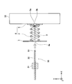
- FIG. 4 shows a cross-sectional view of the spring unit 6 before compression.
- Reference numeral 35 denotes a jig used when the spring unit 6 is compressed.
- the first plate 5 of the spring unit 6 is applied to the jig 35, and the lock pin 30 is inserted into the through passage 9 from the second plate 4 side.
- the stopper 31 is larger than the central hole 4a. Therefore, when the lock pin 30 is pushed, the stopper 31 pushes the second plate 4 and the spring unit 6 (coil spring 3) is compressed.
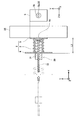
- FIG. 5 shows a state in which the lock pin 30 is pushed in until the hook 33 of the lock pin 30 passes through the elliptical hole 5 a of the first plate 5.
- the phantom line in FIG. 5 shows the lock pin in the initial position, the second plate before being pushed in, and a part of the coil spring.
- the spring unit 6 is compressed to the length L2.
- the hook 33 is accommodated in a recess 5 b provided in the first plate 5 and does not protrude forward from the first plate 5. That is, by providing the recess 5 b, the hook 33 does not get in the way when the spring unit 6 is brought into contact with the end surface 20 a of the semiconductor stacked unit 20.
- the length L2 is shorter than the gap width L1 (see FIG. 7) when the semiconductor multilayer unit 20 is placed on the frame 12.
- the right side of FIG. 5 is a view of the first plate 5 viewed from the X direction.
- the hook 33 and the elliptical hole 5a appear to overlap.
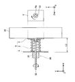
- FIG. 6 shows a state where the lock pin 30 is rotated 90 degrees.
- the hook 33 is caught on the edge of the elliptical hole 5 a of the first plate 5, and the lock pin 30 cannot be removed. That is, the spring unit 6 is held in a compressed state.
- This step is a step of arranging the semiconductor laminated unit 20 and the compressed spring unit 6 on the frame 12.
- FIG. 7 shows a plan view when the semiconductor laminated unit 20 and the spring unit 6 are arranged on the frame 12.
- the semiconductor stacked unit 20 is disposed between the wall 14 of the frame 12 and the support column 13.
- the spring unit 6 is inserted between the semiconductor stacked unit 20 and the support column 13.
- the length L2 of the compressed spring unit 6 is shorter than the gap width L1 between the end surface 20a of the semiconductor stacked unit 20 and the support column 13, the spring unit 6 can be easily inserted.
- This step is a step of removing the lock pin 30 to release the spring unit 6 and applying pressure to the semiconductor multilayer unit 20 to fix the semiconductor multilayer unit 20 to the frame 12.
- the stopper 31 of the lock pin 30 can slide with respect to the rod 32. First, the stopper 31 is released from the rod 32. Then, the stopper 31 is pushed back by the coil spring 3 via the second plate 4.
- FIG. 8 shows a state where the spring unit 6 is released. As shown in FIG. 8, the stopper 31 is retracted compared to FIG. Note that a damper is incorporated in the stopper 31, and the stopper 31 is pushed backward by the coil spring 3. As the stopper 31 moves backward, the second plate 4 also moves backward.
- the semiconductor stacked unit 20 When the second plate 4 comes into contact with the support 13, the semiconductor stacked unit 20 receives pressure by the spring unit 6 between the support 13 and the wall 14. Finally, the rod 32 is reversed 90 degrees, the hook 33 is disengaged, and the lock pin 30 is removed from the spring unit 6 (see FIG. 8). Thus, the semiconductor stacked unit 20 is fixed to the frame 12.
- the spring unit 6 that applies pressure to the semiconductor stacked unit 20 has a recess 5 b and an elliptical hole 5 a in the first plate 5 that contacts the semiconductor stacked unit 20.
- the spring unit 6 can be held in a compressed state by the lock pin 30 without the hook 33 coming out from the front of the first plate 5. Therefore, the spring unit 6 can be inserted between the support 13 and the semiconductor stacked unit 20 while the compressed state is maintained by the lock pin 30.
- the first plate 5 uniformly presses the semiconductor multilayer unit 20 by releasing the lock of the spring unit 6. Can do. Therefore, the semiconductor module 22 and the cooler 21 can be uniformly adhered.
- the fact that the stopper 31 of the lock pin 30 includes a damper also contributes to pressing the semiconductor multilayer unit 20 uniformly. Transient pressure when the spring is released can be absorbed (by the stopper incorporating the damper being pushed back slowly by the coil spring), and the cooler and structure (grease) are not damaged.
- the lock pin 30 can be used repeatedly.
- the spring unit 6 uses the lock pin 30 having the hook 33 without using bolts or screws to maintain the compressed state. If bolts are used, dust may be generated when the bolts are removed from the screw holes. Since the technology of the embodiment does not use bolts or screws, generation of dust can be suppressed.
- FIG. 9 shows a perspective view of an inverter 2a (power converter) of a modification.
- the case 112 corresponds to a frame.
- Three slits 112 a and 112 b are provided on one side surface of the case 112.
- the slit 112b is a slit for guiding the refrigerant supply pipe 24 and the discharge pipe 23 to the outside of the case.
- the slit 112 a is provided to secure a space for the lock pin inserted through the spring unit 6 when the semiconductor laminated unit 20 is attached.
- the side edge of the slit 112a corresponds to the column 13 in the inverter 2 of FIG.
- the second plate 4 is locked to the side edge of the slit 112a.
- the inverter 2a has the same effect as the inverter 2 described above.
- FIG. 10 shows a perspective view of an inverter 2b (power converter) of another modification.
- the inverter 2b corresponds to the inverter 2 in FIG. 1 in which the frame 12 is replaced with the case 112.
- the spring unit 6 is inserted between one end surface 20 a of the semiconductor stacked unit 20 and the support column 13.
- Case 112 corresponds to a frame.
- Three slits 112 a and 112 b are provided on one side surface of the case 112.
- the slit 112b is a slit for guiding the refrigerant supply pipe 24 and the discharge pipe 23 to the outside of the case.
- the slit 112 a is provided to secure a space for removing the lock pin inserted through the spring unit 6 when the semiconductor stacked unit 20 is attached.
- the inverter 2b has the same effect as the inverter 2 described above.
- the spring unit 6 of the example employs the coil spring 3.
- the spring used for the spring unit 6 is not limited to a coil spring.
- a leaf spring having a hole in the center may be used.
- the central hole corresponds to the opening of the through passage that penetrates the spring unit.
- the inverters 2 and 2a in the embodiment correspond to an example of a power converter.
- the technology disclosed in the present specification can also be applied to another type of power conversion device such as a voltage converter.
Landscapes
- Engineering & Computer Science (AREA)
- Power Engineering (AREA)
- Inverter Devices (AREA)
Abstract
Description
Claims (4)
- 半導体素子を収めた平板型の半導体モジュールと平板型の冷却器が交互に積層した半導体積層ユニットと、
半導体積層ユニットを取り付けるためのフレームと、
半導体積層ユニットの積層方向の一端と、フレームに設けられた壁又は支柱との間に嵌挿されており、半導体積層ユニットに圧力を加えるスプリングユニットと、を備えており、
前記スプリングユニットは、
半導体積層ユニットの端面に当接するとともに、半導体積層ユニットの端面との間に隙間を有するように窪みが設けられている第1プレートと、
フレームの壁又は支柱に当接する第2プレートと、
第1及び第2プレートの間に挟まれているスプリングと、
を備えているとともに、
前記窪みの底面を通りスプリングユニット全体を貫通する貫通路が設けられていることを特徴とする電力変換装置。 - 前記フレームは、半導体積層ユニットを収めるケースであることを特徴とする請求項1に記載の電力変換装置。
- 前記スプリングはコイルスプリングであることを特徴とする請求項1又は2に記載の電力変換装置。
- 請求項1から3のいずれか1項に記載の電力変換装置の製造方法であり、
先端にフックを有するロックピンを第2プレート側から貫通路に挿入し、スプリングユニットを圧縮し、第1プレートの貫通路開口の縁にロックピンのフックを引っ掛けてスプリングユニットを圧縮状態に保持し、
半導体積層ユニットをフレーム上に置くとともに、フレームの壁又は支柱と半導体積層ユニットの端面との間に、圧縮状態に保持されたスプリングユニットを置き、
ロックピンを外してスプリングユニットを解放し、半導体積層ユニットに圧力を加え、半導体積層ユニットを固定する、
ことを特徴とする電力変換装置の製造方法。
Priority Applications (5)
| Application Number | Priority Date | Filing Date | Title |
|---|---|---|---|
| JP2013555025A JP5725209B2 (ja) | 2012-01-23 | 2012-01-23 | 電力変換装置及びその製造方法 |
| CN201280067862.5A CN104067501A (zh) | 2012-01-23 | 2012-01-23 | 电力转换装置及其制造方法 |
| EP12866817.5A EP2808988A4 (en) | 2012-01-23 | 2012-01-23 | CURRENT TRANSFORMERS AND MANUFACTURING METHOD THEREFOR |
| US14/367,868 US9105597B2 (en) | 2012-01-23 | 2012-01-23 | Electric power converter and method of manufacturing the same |
| PCT/JP2012/051320 WO2013111261A1 (ja) | 2012-01-23 | 2012-01-23 | 電力変換装置及びその製造方法 |
Applications Claiming Priority (1)
| Application Number | Priority Date | Filing Date | Title |
|---|---|---|---|
| PCT/JP2012/051320 WO2013111261A1 (ja) | 2012-01-23 | 2012-01-23 | 電力変換装置及びその製造方法 |
Publications (1)
| Publication Number | Publication Date |
|---|---|
| WO2013111261A1 true WO2013111261A1 (ja) | 2013-08-01 |
Family
ID=48873033
Family Applications (1)
| Application Number | Title | Priority Date | Filing Date |
|---|---|---|---|
| PCT/JP2012/051320 Ceased WO2013111261A1 (ja) | 2012-01-23 | 2012-01-23 | 電力変換装置及びその製造方法 |
Country Status (5)
| Country | Link |
|---|---|
| US (1) | US9105597B2 (ja) |
| EP (1) | EP2808988A4 (ja) |
| JP (1) | JP5725209B2 (ja) |
| CN (1) | CN104067501A (ja) |
| WO (1) | WO2013111261A1 (ja) |
Cited By (5)
| Publication number | Priority date | Publication date | Assignee | Title |
|---|---|---|---|---|
| JP2015220977A (ja) * | 2014-05-14 | 2015-12-07 | 現代自動車株式会社Hyundaimotor Company | 自動車のハイブリッド電力制御装置 |
| JP2018101691A (ja) * | 2016-12-20 | 2018-06-28 | トヨタ自動車株式会社 | 電子機器 |
| KR20200052604A (ko) * | 2018-11-07 | 2020-05-15 | 현대모비스 주식회사 | 전력변환장치 |
| JP2020178413A (ja) * | 2019-04-16 | 2020-10-29 | 株式会社デンソー | 車載用電力変換装置 |
| JP7183373B1 (ja) | 2021-11-15 | 2022-12-05 | 三菱電機株式会社 | 電力変換装置 |
Families Citing this family (10)
| Publication number | Priority date | Publication date | Assignee | Title |
|---|---|---|---|---|
| JP5655846B2 (ja) * | 2012-12-04 | 2015-01-21 | 株式会社デンソー | 電力変換装置 |
| JP6127937B2 (ja) * | 2013-11-28 | 2017-05-17 | 株式会社デンソー | 電力変換装置 |
| USD837623S1 (en) * | 2015-10-20 | 2019-01-08 | LWE, Inc. | Load beam for press pack clamp |
| JP6500756B2 (ja) * | 2015-11-17 | 2019-04-17 | 株式会社デンソー | 電力変換装置 |
| JP6647991B2 (ja) * | 2016-09-05 | 2020-02-14 | 株式会社デンソー | 電力変換装置 |
| CN107872213A (zh) * | 2017-12-06 | 2018-04-03 | 苏州喷声电子科技有限公司 | 一种具有散热和快速切换的晶闸管开关 |
| JP7014626B2 (ja) * | 2018-02-07 | 2022-02-01 | 株式会社Soken | 半導体装置 |
| JP7099385B2 (ja) * | 2019-03-28 | 2022-07-12 | 株式会社デンソー | 加圧部材 |
| JP7133762B2 (ja) * | 2019-06-07 | 2022-09-09 | 株式会社デンソー | 電力変換装置とその製造方法 |
| DE102021002237A1 (de) | 2020-05-15 | 2021-11-18 | Sew-Eurodrive Gmbh & Co Kg | Antrieb mit Anschlusskasten |
Citations (5)
| Publication number | Priority date | Publication date | Assignee | Title |
|---|---|---|---|---|
| JP2011167028A (ja) | 2010-02-15 | 2011-08-25 | Denso Corp | 電力変換装置 |
| JP2011200057A (ja) | 2010-03-23 | 2011-10-06 | Denso Corp | 電力変換装置及びその製造方法 |
| JP2011211771A (ja) | 2010-03-29 | 2011-10-20 | Denso Corp | 電力変換装置及びその製造方法 |
| JP2011211853A (ja) * | 2010-03-30 | 2011-10-20 | Denso Corp | 電力変換装置 |
| JP2011239623A (ja) * | 2010-05-13 | 2011-11-24 | Denso Corp | 電力変換装置及びその製造方法 |
Family Cites Families (8)
| Publication number | Priority date | Publication date | Assignee | Title |
|---|---|---|---|---|
| JPS58139453A (ja) * | 1982-02-15 | 1983-08-18 | Toshiba Corp | 横置形半導体スタツク |
| US4769744A (en) * | 1983-08-04 | 1988-09-06 | General Electric Company | Semiconductor chip packages having solder layers of enhanced durability |
| FR2550887B1 (fr) * | 1983-08-19 | 1986-11-07 | Jeumont Schneider | Element pretare pour le maintien en place et le serrage de semi-conducteurs et de radiateurs disposes en colonne par alternance |
| US6058014A (en) * | 1998-10-13 | 2000-05-02 | International Business Machines Corporation | Enhanced mounting hardware for a circuit board |
| DE19903245A1 (de) * | 1999-01-27 | 2000-08-03 | Asea Brown Boveri | Leistungshalbleitermodul |
| CN101663752B (zh) * | 2007-03-30 | 2011-10-26 | Abb技术有限公司 | 功率半导体装置及设置有功率半导体装置的半导体阀 |
| WO2012070129A1 (ja) | 2010-11-24 | 2012-05-31 | トヨタ自動車株式会社 | 積層型冷却器 |
| JP2014078599A (ja) * | 2012-10-10 | 2014-05-01 | Denso Corp | 電力変換装置 |
-
2012
- 2012-01-23 CN CN201280067862.5A patent/CN104067501A/zh active Pending
- 2012-01-23 EP EP12866817.5A patent/EP2808988A4/en not_active Withdrawn
- 2012-01-23 JP JP2013555025A patent/JP5725209B2/ja active Active
- 2012-01-23 WO PCT/JP2012/051320 patent/WO2013111261A1/ja not_active Ceased
- 2012-01-23 US US14/367,868 patent/US9105597B2/en not_active Expired - Fee Related
Patent Citations (5)
| Publication number | Priority date | Publication date | Assignee | Title |
|---|---|---|---|---|
| JP2011167028A (ja) | 2010-02-15 | 2011-08-25 | Denso Corp | 電力変換装置 |
| JP2011200057A (ja) | 2010-03-23 | 2011-10-06 | Denso Corp | 電力変換装置及びその製造方法 |
| JP2011211771A (ja) | 2010-03-29 | 2011-10-20 | Denso Corp | 電力変換装置及びその製造方法 |
| JP2011211853A (ja) * | 2010-03-30 | 2011-10-20 | Denso Corp | 電力変換装置 |
| JP2011239623A (ja) * | 2010-05-13 | 2011-11-24 | Denso Corp | 電力変換装置及びその製造方法 |
Non-Patent Citations (1)
| Title |
|---|
| See also references of EP2808988A4 |
Cited By (11)
| Publication number | Priority date | Publication date | Assignee | Title |
|---|---|---|---|---|
| JP2015220977A (ja) * | 2014-05-14 | 2015-12-07 | 現代自動車株式会社Hyundaimotor Company | 自動車のハイブリッド電力制御装置 |
| DE102014225033B4 (de) | 2014-05-14 | 2024-02-08 | Hyundai Motor Company | Hybrid-Energie-Steuervorrichtung für ein Fahrzeug |
| DE102014225033B8 (de) | 2014-05-14 | 2024-04-18 | Hyundai Motor Company | Hybrid-Energie-Steuervorrichtung für ein Fahrzeug |
| JP2018101691A (ja) * | 2016-12-20 | 2018-06-28 | トヨタ自動車株式会社 | 電子機器 |
| KR20200052604A (ko) * | 2018-11-07 | 2020-05-15 | 현대모비스 주식회사 | 전력변환장치 |
| KR102619731B1 (ko) * | 2018-11-07 | 2024-01-02 | 현대모비스 주식회사 | 전력변환장치 |
| JP2020178413A (ja) * | 2019-04-16 | 2020-10-29 | 株式会社デンソー | 車載用電力変換装置 |
| JP7218662B2 (ja) | 2019-04-16 | 2023-02-07 | 株式会社デンソー | 車載用電力変換装置 |
| JP7183373B1 (ja) | 2021-11-15 | 2022-12-05 | 三菱電機株式会社 | 電力変換装置 |
| JP2023072804A (ja) * | 2021-11-15 | 2023-05-25 | 三菱電機株式会社 | 電力変換装置 |
| US12309982B2 (en) | 2021-11-15 | 2025-05-20 | Mitsubishi Electric Corporation | Power conversion device |
Also Published As
| Publication number | Publication date |
|---|---|
| US20150123261A1 (en) | 2015-05-07 |
| JP5725209B2 (ja) | 2015-05-27 |
| JPWO2013111261A1 (ja) | 2015-05-11 |
| CN104067501A (zh) | 2014-09-24 |
| EP2808988A1 (en) | 2014-12-03 |
| EP2808988A4 (en) | 2015-11-25 |
| US9105597B2 (en) | 2015-08-11 |
Similar Documents
| Publication | Publication Date | Title |
|---|---|---|
| JP5725209B2 (ja) | 電力変換装置及びその製造方法 | |
| JP5531999B2 (ja) | 電力変換装置 | |
| JP4900202B2 (ja) | 電力変換装置 | |
| JP4525582B2 (ja) | 電力変換装置 | |
| JP5494210B2 (ja) | 電力変換装置及びその製造方法 | |
| JP2013115907A (ja) | 電力変換装置 | |
| JP5445041B2 (ja) | 電力変換装置 | |
| JP2008245472A (ja) | 電力変換装置 | |
| JP4325486B2 (ja) | 電力変換ユニット | |
| JP2016063641A (ja) | 電力変換装置 | |
| JP2011200057A (ja) | 電力変換装置及びその製造方法 | |
| JP5835145B2 (ja) | 半導体積層ユニットとその製造方法 | |
| JP2011211853A (ja) | 電力変換装置 | |
| JP2015186344A (ja) | 電力変換装置 | |
| JP5782845B2 (ja) | 電力変換装置及びその製造方法 | |
| JP5772618B2 (ja) | 電力変換装置とその製造方法 | |
| JP2011167028A (ja) | 電力変換装置 | |
| JP2013146168A (ja) | 電力変換装置とその製造方法 | |
| JP2018182075A (ja) | コンデンサモジュール | |
| JP2013118334A (ja) | 半導体冷却器 | |
| JP2018137918A (ja) | 電力変換装置 | |
| JP5838926B2 (ja) | 電力変換装置とその製作方法 | |
| JP5935586B2 (ja) | 半導体積層ユニットの製造方法 | |
| JP5510350B2 (ja) | 電力変換装置及びその製造方法 | |
| JP5765208B2 (ja) | 電力変換装置およびその製造方法 |
Legal Events
| Date | Code | Title | Description |
|---|---|---|---|
| 121 | Ep: the epo has been informed by wipo that ep was designated in this application |
Ref document number: 12866817 Country of ref document: EP Kind code of ref document: A1 |
|
| ENP | Entry into the national phase |
Ref document number: 2013555025 Country of ref document: JP Kind code of ref document: A |
|
| WWE | Wipo information: entry into national phase |
Ref document number: 14367868 Country of ref document: US |
|
| WWE | Wipo information: entry into national phase |
Ref document number: 2012866817 Country of ref document: EP |
|
| NENP | Non-entry into the national phase |
Ref country code: DE |