WO2013114678A1 - 絶縁回路及び通信機器 - Google Patents
絶縁回路及び通信機器 Download PDFInfo
- Publication number
- WO2013114678A1 WO2013114678A1 PCT/JP2012/076084 JP2012076084W WO2013114678A1 WO 2013114678 A1 WO2013114678 A1 WO 2013114678A1 JP 2012076084 W JP2012076084 W JP 2012076084W WO 2013114678 A1 WO2013114678 A1 WO 2013114678A1
- Authority
- WO
- WIPO (PCT)
- Prior art keywords
- pattern
- plan
- patterns
- layer
- view
- Prior art date
- Legal status (The legal status is an assumption and is not a legal conclusion. Google has not performed a legal analysis and makes no representation as to the accuracy of the status listed.)
- Ceased
Links
Images



Classifications
-
- H—ELECTRICITY
- H05—ELECTRIC TECHNIQUES NOT OTHERWISE PROVIDED FOR
- H05K—PRINTED CIRCUITS; CASINGS OR CONSTRUCTIONAL DETAILS OF ELECTRIC APPARATUS; MANUFACTURE OF ASSEMBLAGES OF ELECTRICAL COMPONENTS
- H05K1/00—Printed circuits
- H05K1/02—Details
- H05K1/0213—Electrical arrangements not otherwise provided for
- H05K1/0237—High frequency adaptations
- H05K1/025—Impedance arrangements, e.g. impedance matching, reduction of parasitic impedance
-
- H—ELECTRICITY
- H01—ELECTRIC ELEMENTS
- H01P—WAVEGUIDES; RESONATORS, LINES, OR OTHER DEVICES OF THE WAVEGUIDE TYPE
- H01P1/00—Auxiliary devices
- H01P1/20—Frequency-selective devices, e.g. filters
-
- H—ELECTRICITY
- H01—ELECTRIC ELEMENTS
- H01P—WAVEGUIDES; RESONATORS, LINES, OR OTHER DEVICES OF THE WAVEGUIDE TYPE
- H01P1/00—Auxiliary devices
- H01P1/20—Frequency-selective devices, e.g. filters
- H01P1/201—Filters for transverse electromagnetic waves
- H01P1/203—Strip line filters
-
- H—ELECTRICITY
- H01—ELECTRIC ELEMENTS
- H01P—WAVEGUIDES; RESONATORS, LINES, OR OTHER DEVICES OF THE WAVEGUIDE TYPE
- H01P5/00—Coupling devices of the waveguide type
-
- H—ELECTRICITY
- H05—ELECTRIC TECHNIQUES NOT OTHERWISE PROVIDED FOR
- H05K—PRINTED CIRCUITS; CASINGS OR CONSTRUCTIONAL DETAILS OF ELECTRIC APPARATUS; MANUFACTURE OF ASSEMBLAGES OF ELECTRICAL COMPONENTS
- H05K1/00—Printed circuits
- H05K1/02—Details
- H05K1/0213—Electrical arrangements not otherwise provided for
- H05K1/0237—High frequency adaptations
- H05K1/025—Impedance arrangements, e.g. impedance matching, reduction of parasitic impedance
- H05K1/0253—Impedance adaptations of transmission lines by special lay-out of power planes, e.g. providing openings
-
- H—ELECTRICITY
- H05—ELECTRIC TECHNIQUES NOT OTHERWISE PROVIDED FOR
- H05K—PRINTED CIRCUITS; CASINGS OR CONSTRUCTIONAL DETAILS OF ELECTRIC APPARATUS; MANUFACTURE OF ASSEMBLAGES OF ELECTRICAL COMPONENTS
- H05K1/00—Printed circuits
- H05K1/02—Details
- H05K1/11—Printed elements for providing electric connections to or between printed circuits
- H05K1/115—Via connections; Lands around holes or via connections
-
- H—ELECTRICITY
- H05—ELECTRIC TECHNIQUES NOT OTHERWISE PROVIDED FOR
- H05K—PRINTED CIRCUITS; CASINGS OR CONSTRUCTIONAL DETAILS OF ELECTRIC APPARATUS; MANUFACTURE OF ASSEMBLAGES OF ELECTRICAL COMPONENTS
- H05K1/00—Printed circuits
- H05K1/02—Details
- H05K1/0213—Electrical arrangements not otherwise provided for
- H05K1/0216—Reduction of cross-talk, noise or electromagnetic interference
- H05K1/0218—Reduction of cross-talk, noise or electromagnetic interference by printed shielding conductors, ground planes or power plane
- H05K1/0224—Patterned shielding planes, ground planes or power planes
- H05K1/0225—Single or multiple openings in a shielding, ground or power plane
-
- H—ELECTRICITY
- H05—ELECTRIC TECHNIQUES NOT OTHERWISE PROVIDED FOR
- H05K—PRINTED CIRCUITS; CASINGS OR CONSTRUCTIONAL DETAILS OF ELECTRIC APPARATUS; MANUFACTURE OF ASSEMBLAGES OF ELECTRICAL COMPONENTS
- H05K1/00—Printed circuits
- H05K1/02—Details
- H05K1/0213—Electrical arrangements not otherwise provided for
- H05K1/0216—Reduction of cross-talk, noise or electromagnetic interference
- H05K1/0218—Reduction of cross-talk, noise or electromagnetic interference by printed shielding conductors, ground planes or power plane
- H05K1/0224—Patterned shielding planes, ground planes or power planes
- H05K1/0227—Split or nearly split shielding or ground planes
-
- H—ELECTRICITY
- H05—ELECTRIC TECHNIQUES NOT OTHERWISE PROVIDED FOR
- H05K—PRINTED CIRCUITS; CASINGS OR CONSTRUCTIONAL DETAILS OF ELECTRIC APPARATUS; MANUFACTURE OF ASSEMBLAGES OF ELECTRICAL COMPONENTS
- H05K2201/00—Indexing scheme relating to printed circuits covered by H05K1/00
- H05K2201/09—Shape and layout
- H05K2201/09209—Shape and layout details of conductors
- H05K2201/09654—Shape and layout details of conductors covering at least two types of conductors provided for in H05K2201/09218 - H05K2201/095
- H05K2201/09727—Varying width along a single conductor; Conductors or pads having different widths
Definitions
- the present invention relates to an insulation circuit and a communication device.
- This application claims priority based on Japanese Patent Application No. 2012-021201 filed on February 2, 2012, the contents of which are incorporated herein by reference.
- DCS Distributed Control System
- Most field devices measuring instruments such as pressure transmitters and operation devices
- Wireless field devices that perform the above are also realized.
- the electrical circuit (electronic circuit) provided inside the device is designed not to be an ignition source of the combustible gas not only in a normal state but also in an expected accident.
- the explosion-proof standard it is necessary to have a pressure- and explosion-proof structure so that even if an explosion occurs inside the device, the flame caused by the explosion does not ignite the external combustible gas.
- Patent Document 1 discloses a low-cost antenna device that can be attached to a fully enclosed container having an explosion-proof structure used in hazardous locations.
- this antenna apparatus in order to satisfy the intrinsically safe explosion-proof standard, two blocking capacitors are connected in series via a printed pattern on one surface of a printed circuit board housed in a housing, and are mounted on the other surface. Two blocking capacitors are mounted connected in series via a printed pattern.
- the ground in the device is separated into a signal ground and a frame ground, and these are galvanically isolated in order to prevent failure of the electronic circuit while meeting the intrinsic safety explosion-proof standards described above. Need to be done.
- the main methods of DC-insulating the signal ground and the frame ground are a method using a chip capacitor and a method using a high-frequency balun. That is, by providing a chip capacitor or a high frequency balun between the signal ground and the frame ground or between the signal lines, the signal ground and the frame ground are galvanically isolated.
- the present invention provides an insulation circuit and a communication device that can improve noise resistance while satisfying intrinsic safety explosion-proof standards without using discrete elements such as chip capacitors.
- the insulating circuit is formed on the first layer of the substrate and receives a high frequency signal, and is formed on the first layer side by side with the first pattern, and outputs the high frequency signal received by the first pattern.
- a second pattern a third pattern formed on a second layer different from the first layer of the substrate so as to overlap each of the first and second patterns in plan view, and connected to a signal ground;
- a fourth pattern that is formed on the second layer so as to overlap each of the first and second patterns when viewed, and is connected to a frame ground.
- the third pattern has a first slit extending in a direction in which the first and second patterns extend between a portion overlapping the first pattern in plan view and a portion overlapping the second pattern in plan view.
- a slit may be formed.
- the third pattern has at least one first opening formed along at least one side of a portion overlapping the second pattern in plan view, and the fourth pattern has the first pattern in plan view. You may have at least 1 2nd opening part formed along at least one side of the part which overlaps with a pattern.
- the insulating circuit is formed in the first layer so as to overlap the third pattern in plan view, one end of which is connected to the first pattern, and the other end is connected to the third pattern through a first via.
- a fifth pattern to be connected is formed on the first layer so as to overlap the fourth pattern in plan view, one end of which is connected to the second pattern, and the other end is connected to the second pattern via a second via. And a sixth pattern connected to the four patterns.
- the third pattern and the fourth pattern may be separated from each other by a distance defined in at least an intrinsically safe explosion-proof standard in the second layer.
- the substrate may be a double-sided substrate in which a pattern is formed on the first layer that is the front surface and the second layer that is the back surface.
- the substrate may be a multilayer substrate in which one or more layers in which a pattern is formed are provided between the front surface and the back surface.
- a substrate having a predetermined thickness may be interposed between the first and second patterns and the third and fourth patterns.
- the first pattern and the second pattern may be linear and may include a plurality of pads for matching impedance. One end of each of the first pattern and the second pattern may have a predetermined characteristic impedance, and the other end may be an open end.
- the first opening is formed along both sides of a portion where the second pattern and the third pattern overlap, and the second opening is a portion where the first pattern and the fourth pattern overlap. It may be formed along both sides.
- the first opening may be formed along one side of a portion where the second pattern and the third pattern overlap.
- the second opening may be formed along one side of a portion where the first pattern and the fourth pattern overlap.
- a communication device that performs at least one of transmission and reception of a high-frequency signal, formed on a first layer of a substrate, and formed on the first layer side by side with the first pattern for receiving the high-frequency signal and the first pattern.
- the second pattern for outputting the high-frequency signal received by the first pattern is formed on a second layer different from the first layer of the substrate so as to overlap each of the first and second patterns in a plan view.
- a third pattern connected to the signal ground, and formed in the second layer side by side in the third pattern so as to overlap each of the first and second patterns in plan view, and connected to the frame ground.
- the third pattern has a first slit extending in a direction in which the first and second patterns extend between a portion overlapping the first pattern in plan view and a portion overlapping the second pattern in plan view.
- a second pattern extending in a direction in which the first and second patterns extend between a portion overlapping the first pattern in plan view and a portion overlapping the second pattern in plan view.
- a slit may be formed.
- the third pattern has at least one first opening formed along at least one side of a portion overlapping the second pattern in plan view
- the fourth pattern has the first pattern in plan view. You may have at least 1 2nd opening part formed along at least one side of the part which overlaps with a pattern.
- the insulating circuit is formed in the first layer so as to overlap the third pattern in plan view, one end of which is connected to the first pattern, and the other end is connected to the third pattern through a first via.
- a fifth pattern to be connected is formed on the first layer so as to overlap the fourth pattern in plan view, one end of which is connected to the second pattern, and the other end is connected to the second pattern via a second via.
- a sixth pattern connected to the four patterns.
- the third pattern and the fourth pattern may be separated from each other by a distance defined in at least an intrinsically safe explosion-proof standard in the second layer.
- the first pattern to which the high-frequency signal is input and the second pattern from which the high-frequency signal is output are formed side by side on the first layer of the substrate, and the third pattern and the frame connected to the signal ground
- the fourth pattern connected to the ground is formed side by side in the second layer so as to overlap each of the first and second patterns in plan view.
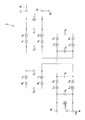
- FIG. 1 is a plan perspective view showing a configuration of an insulating circuit according to an embodiment of the present invention.
- an insulating circuit 1 according to an embodiment of the present invention includes four patterns 11 to 14 (a first pattern 11, a second pattern 12, and the like) formed on a substrate (not shown) having at least two layers.
- the third pattern 13 and the fourth pattern 14) and two auxiliary patterns 15 and 16 are included.
- the insulating circuit 1 transmits a required high-frequency signal while DC-insulating the signal ground SG and the frame ground FG (both not shown in FIG. 1, see FIG. 2).
- the substrate on which the patterns 11 to 14 and the auxiliary patterns 15 and 16 are formed has patterns on the front surface (first layer) and the back surface (second layer).
- the substrate on which the patterns 11 to 14 and the auxiliary patterns 15 and 16 are formed is not limited to a double-sided substrate, and one or more layers in which a pattern is formed are provided between the front surface and the back surface.
- a multilayer substrate may be used.
- this substrate for example, a glass epoxy substrate, a ceramic substrate, a Teflon (registered trademark) substrate, or the like can be used.
- the patterns 11 and 12 and the auxiliary patterns 15 and 16 are formed on the surface of the substrate using a metal having a small electrical resistance such as copper (Cu) or aluminum (Al).
- the patterns 13 and 14 are formed on the back surface of the substrate using the same metal as the patterns 11 and 12 and the auxiliary patterns 15 and 16.
- FIG. 1 shows a state in which the patterns 11 and 12 and the auxiliary patterns 15 and 16 and the patterns 13 and 14 are overlapped in a plan view, but actually the patterns 11 and 12 and the auxiliary patterns 15 and 16 and the pattern are overlapped.
- a substrate having a predetermined thickness is interposed between 13 and 14.
- a direction along the direction in which the patterns 11 and 12 extend is referred to as a longitudinal direction D1
- a direction that intersects the longitudinal direction D1 and is parallel to the surface of the substrate is referred to as an intersecting direction D2.
- the pattern 11 is a linear pattern extending in the longitudinal direction D1, and a high frequency signal to be transmitted is input.
- a plurality of pads (hereinafter referred to as impedance matching pads) 11a to 11g for matching impedance are formed in the pattern 11, and a high-frequency signal to be transmitted is input to one end T1 of the pattern 11.
- impedance matching pads 11a formed closest to one end T1 of the pattern 11 and the impedance matching pad 11g formed on the other end T2 of the pattern 11 are more than the other impedance matching pads 11b to 11f. Largely formed.
- the pattern 11 is designed so that one end T1 thereof has a predetermined characteristic impedance (for example, 50 ⁇ ) and the other end T2 is an open end. That is, the pattern 11 is designed so that a high-frequency signal input from one end T1 is easily radiated from the other end T2.
- the number and size of the impedance matching pads 11a to 11g formed on the pattern 11 can be arbitrarily set according to the required power transmission efficiency.
- the pattern 12 is a linear pattern extending in the longitudinal direction D1 formed side by side in the pattern 11 at a predetermined interval in the intersecting direction D2, and a high-frequency signal input to the pattern 11 is output. Similar to the pattern 11, the pattern 12 is formed with a plurality of impedance matching pads 12a to 12f for matching impedance, and a high-frequency signal is output from one end T4 thereof. In the example shown in FIG. 1, these impedance matching pads 12a to 12f are formed to have substantially the same size.
- the pattern 12 is designed so that one end T4 thereof has the characteristic impedance described above and the other end T3 is an open end.
- the number and size of the impedance matching pads 12a to 12f formed on the pattern 12 are arbitrarily set according to the required power transmission efficiency, similarly to the impedance matching pads 11a to 11g formed on the pattern 11. Is possible.
- the pattern 13 is a substantially rectangular pattern formed so as to overlap each of the patterns 11 and 12 in plan view, and is connected to the signal ground SG described above.
- the pattern 13 is formed with slits (hereinafter referred to as impedance matching slits) 13a and a plurality of opening patterns 13b (openings) for adjusting transmission characteristics within and outside the band of the high-frequency signal to be transmitted.
- the impedance matching slit 13a is a rectangular slit extending in the longitudinal direction D1, and at the right end of the pattern 13 in the drawing, a portion where the patterns 11, 13 overlap in a plan view and a portion where the patterns 12, 13 overlap in a plan view. Is formed between.
- the opening pattern 13b is an opening having a substantially rectangular shape in plan view, and a plurality of opening patterns 13b are formed along both sides of the portion where the patterns 12 and 13 overlap.
- the shape and size of the impedance matching slit 13a and the opening pattern 13b and the number of the opening patterns 13b can be arbitrarily set according to the required transmission characteristics.
- the opening pattern 13b is not necessarily formed along both sides of the portion where the patterns 12 and 13 overlap, and may be formed only along one side.
- the pattern 14 is a substantially rectangular pattern formed side by side in the pattern 13 so as to overlap each of the patterns 11 and 12 in plan view, and is connected to the frame ground FG described above. Similar to the pattern 13, the pattern 14 is formed with an impedance matching slit 14 a and a plurality of opening patterns 14 b (openings) for adjusting the transmission characteristics of the high-frequency signal to be transmitted within and outside the band.
- the impedance matching slit 14a is a rectangular slit extending in the longitudinal direction D1, and at the left end of the pattern 14 in the drawing, a portion where the patterns 11, 14 overlap in a plan view and a portion where the patterns 12, 14 overlap in a plan view. Is formed between.
- the opening pattern 14b is an opening having a substantially rectangular shape in plan view, and a plurality of opening patterns 14b are formed along both sides of the portion where the patterns 11 and 14 overlap.
- the shape and size of the impedance matching slit 14a and the opening pattern 14b, and the number of the opening patterns 14b can be arbitrarily set according to required transmission characteristics.
- the opening pattern 14b is not necessarily formed along both sides of the portion where the patterns 11 and 14 overlap, and may be formed only along one side.
- the portions where the patterns 11 and 12 and the patterns 13 and 14 overlap in a plan view have the same structure as the microstrip line, and thus the patterns 11 and 12 formed on the surface of the substrate and the back surface of the substrate.
- the formed patterns 13 and 14 are electromagnetically coupled through the substrate.
- the length in the longitudinal direction D1 of the portion where the patterns 11 and 14 overlap is set to a length which strengthens the electromagnetic coupling of the patterns 11 and 14, and the length in the longitudinal direction D1 of the portion where the patterns 12 and 13 overlap is the pattern
- the length is set to strengthen the electromagnetic couplings 12 and 13.
- the pattern 13 connected to the signal ground SG and the pattern 14 connected to the frame ground FG are separated by at least a distance L1 (for example, 0.5 mm or more) defined by the intrinsically safe explosion-proof standard.
- the auxiliary pattern 15 is formed on the surface of the substrate so as to overlap the pattern 13 in plan view. One end thereof is connected to the pattern 11 and the other end is connected to the pattern 13 through the via V1.
- the auxiliary pattern 15 forms a short stub with respect to the pattern 11 and is provided to adjust transmission characteristics outside the band of the high-frequency signal to be transmitted.
- the auxiliary pattern 16 is formed on the surface of the substrate so as to overlap the pattern 14 in plan view. One end thereof is connected to the pattern 12, and the other end is connected to the pattern 14 via the via V2.
- the auxiliary pattern 16 forms a short stub with respect to the pattern 12, and is provided to adjust the transmission characteristics outside the band of the high-frequency signal to be transmitted.
- FIG. 2 is a circuit diagram showing an equivalent circuit of the insulating circuit shown in FIG.
- a signal line SL to which a high-frequency signal is supplied is connected to one end T1 of the pattern 11
- a signal ground SG is connected to one end T6 of the pattern 13 opposite to the one end T1 of the pattern 11.
- a frame ground FG is connected to one end T7 of the pattern 14 that faces the one end T4 of the pattern 12 that outputs a high-frequency signal.
- the resistance components of the pattern 11 are represented by R 1 and R 2 , and the inductance components are represented by L 1 and L 2 .
- the resistance component of the pattern 12 is represented by R 5 and R 6 , and the inductance component is represented by L 5 and L 6 .
- the resistance component of the pattern 13 is represented by R 3 and R 4 , and the inductance component is represented by L 3 and L 4 .
- the resistance component of the pattern 14 is represented by R 7 and R 8 , and the inductance component is represented by L 7 and L 8 .
- the pattern 15 is represented as an inductance component L in the pattern 16 is represented as an inductance component L out.
- the capacitive component between the patterns 11 and 13 is represented by C 1 and C 2
- the capacitive component between the patterns 11 and 14 is represented by C 3 and C 4
- the capacitive component between the patterns 12 and 13 is represented by C 5 and C 6
- the capacitive component between the patterns 12 and 14 is represented by C 7 and C 8 .
- FIG. 3 is a plan view schematically showing a magnetic field distribution formed in the insulating circuit according to the embodiment of the present invention.
- the magnetic field distribution generated in the patterns 11 and 12 and the auxiliary patterns 15 and 16 formed on the surface of the substrate is represented by white arrows, and the patterns 13 and 14 formed on the back surface of the substrate.
- a leftward magnetic field distribution along the longitudinal direction D1 is generated in the pattern 11 as shown in FIG. Propagates through the pattern 11 to the left and sequentially passes through the impedance matching pads 11a to 11g.
- the high-frequency signal input to one end T1 of the pattern 11 reaches the pattern 13 through the pattern 15 and the via V1 in order, propagates in the pattern 13 in the right direction along the longitudinal direction D1, and immediately below the one end T1 of the pattern 11. Return as a return.
- the pattern 11 is formed so as to overlap with the patterns 13 and 14 in plan view, and is electromagnetically coupled to each of the patterns 13 and 14, so that a part of the high-frequency signal that propagates the pattern 11 to the left propagates to the pattern 13. The rest propagates to the pattern 14.
- the high-frequency signal propagated to the pattern 13 propagates in the pattern 13 in the right direction along the longitudinal direction D1 and returns as a return immediately below one end T1 of the pattern 11.
- the high-frequency signal propagated to the pattern 14 propagates through the pattern 14 so as to avoid the impedance matching slit 14a through the gap of the opening pattern 14b formed in the pattern 14, and the portion where the pattern 12 overlaps in plan view and It reaches just below one end T4 of the pattern 12.
- the pattern 14 is formed so as to overlap with the pattern 12 in plan view and is electromagnetically coupled to the pattern 12, so that the high-frequency signal that reaches the portion where the pattern 12 overlaps in plan view propagates to the pattern 12.
- the high-frequency signal propagated to the pattern 12 propagates the pattern 12 to the right along the longitudinal direction D1 and sequentially passes through the impedance matching pads 12a to 12f.
- the pattern 12 is formed so as to overlap the pattern 13 in a plan view and is electromagnetically coupled to the pattern 13, so that a high-frequency signal propagating rightward through the pattern 12 propagates to the pattern 13.
- the high-frequency signal propagated to the pattern 13 propagates through the pattern 13 so as to avoid the impedance matching slit 13a through the gap of the opening pattern 13b formed in the pattern 13, and reaches just below one end T1 of the pattern 11.
- a high frequency signal input from one end T1 of the pattern 11 is output from one end T4 of the pattern 12.
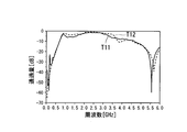
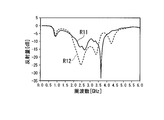
- FIGS. 4A to 4C are diagrams showing reflection / transmission characteristics of an insulating circuit according to an embodiment of the present invention.
- 4A is a diagram showing the pass characteristic
- FIG. 4B is a diagram showing the reflection characteristic on the input side
- FIG. 4C is a diagram showing the reflection characteristic on the output side.
- a curve with a symbol T11 indicates an actual measurement value of the pass characteristic of the insulating circuit 1
- a curve with a symbol T12 indicates a simulation result of the pass characteristic of the insulating circuit 1.
- the curves with the symbols R11 and R21 indicate the actual measurement values of the reflection characteristics of the insulation circuit 1
- the curves with the symbols R12 and R22 are the simulation results of the reflection characteristics of the insulation circuit 1. Is shown.
- the curves T11 and T12, the curves R11 and R12, and the curves R21 and R22 shown in FIGS. 4A to 4C show the following characteristics. That is, the curves T11 and T12 indicate the frequency characteristics of the scattering parameter (S parameter) S21 when the insulating circuit 1 is viewed as a four-terminal circuit. Curves R11 and R12 show the frequency characteristics of the scattering parameter S11, and curves R21 and R22 show the frequency characteristics of the scattering parameter S22.
- FIGS. 4A to 4C first, it can be seen that the measured values of the transmission characteristics and reflection characteristics of the insulation circuit 1 are almost in agreement with the simulation results of the transmission characteristics and reflection characteristics of the insulation circuit 1, respectively.
- FIG. 4A it can be seen that good pass characteristics are obtained over a frequency band of about 1 to 5 GHz. In particular, in the vicinity of 2.5 GHz, it can be seen that most of the input high-frequency signal passes through the insulating circuit 1. Further, referring to FIGS. 4B and 4C, in the vicinity of 2.5 GHz and 3.7 GHz. It can be seen that the amount of reflection is minimal. As described above, from the results shown in FIGS.
- the insulating circuit 1 almost reflects a high-frequency signal having a frequency near 2.5 GHz even if the signal ground SG and the frame ground FG are galvanically insulated. It turns out that it is the characteristic which transmits without doing.
- the pattern 11 to which the high-frequency signal is input and the pattern 12 to which the high-frequency signal is output are formed on the substrate surface.
- a pattern 13 connected to the signal ground SG and a pattern 14 connected to the frame ground FG are formed on the back surface of the substrate so as to overlap.
- the signal ground SG and the frame ground FG can be galvanically isolated without using a discrete element such as a chip capacitor. Thereby, noise resistance performance can be improved while satisfying intrinsically safe explosion-proof standards.
- the insulating circuit 1 shown in FIG. 1 does not need to use a discrete element such as a chip capacitor. For this reason, it is difficult to achieve high-density mounting due to a large mounting integration ratio (occupation area). If the board thickness is large, the wiring pattern becomes thick and loss due to copper loss increases. There is no possibility of various problems such as a lack of appropriate selection of elements), no suitable parts that are both guaranteed withstand voltage, high frequency characteristics and high withstand voltage at the same time, and high cost of the parts. .
- FIG. 5 is a plan view showing an example in which the insulation circuit according to the embodiment of the present invention is modularized.
- the insulation module IM shown in FIG. 5 is connected to the substrate SB having the patterns 11 and 12 formed on the front surface and the patterns 13 and 14 formed on the back surface, the input terminal TM1 connected to the pattern 11, and the pattern 12.
- the input terminal TM1 is attached to the right end portion of the substrate SB, and the output terminal TM2 is attached to the left end portion of the substrate SB.
- the insulation module IM described above can be used as a high-frequency component.
- the insulation module IM can be used to be inserted in a portion that requires DC insulation in a high-frequency circuit.
- the isolation circuit 1 is not limited by the frequency band, frequency characteristics, group delay characteristics, size, shape, substrate type, substrate layer configuration, etc.
- the LTC1 LTCC (Low It can also be realized as a multilayer chip using temperature (Co-fired ceramics) or ceramics.
- the insulating module IM may be formed by covering the substrate SB with a cover (not shown).
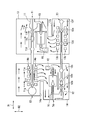
- FIG. 6 is a diagram showing a main configuration of a communication device according to an embodiment of the present invention.
- the communication device 20 according to an embodiment of the present invention includes a casing 21, a power supply unit 22, a communication board 23, and a remote antenna 24, and other devices (not shown) from the remote antenna 24.
- the remote antenna 24 receives a high frequency signal transmitted from another device, thereby communicating with the other device.
- the communication device 20 shown in FIG. 6 is a field device (wireless communication device) capable of wireless communication in conformity with ISA100.11a which is a wireless communication standard for industrial automation established by, for example, the International Society for Measurement and Control (ISA). Field equipment).
- the communication device 20 may be a device that can only transmit a high-frequency signal, or may be a device that can only receive a high-frequency signal.
- the housing 21 is a hollow box member made of a highly rigid metal such as highly rigid aluminum, and is a frame ground FG when grounded.
- the housing 21 has a sealed structure so as to accommodate the power supply unit 22 and the communication board 23 therein and meet the explosion-proof standard.
- the casing 21 is provided with a flameproof connector 21a to which an antenna such as a remote antenna 24 is connected.
- the power supply unit 22 generates a power supply (for example, a DC power supply) IP required inside the communication device 20 using a power supply supplied from the external power supply PS.
- the communication board 23 is a printed board on which a high-frequency signal to be transmitted is output toward the remote antenna 24 and a high-frequency signal received by the remote antenna 24 is input.
- the communication board 23 is provided with a connector C11 to which a connector C12 connected to the flameproof connector 21a of the housing 21 is attached. Note that the communication board 23 is supplied with the power supply IP generated by the power supply unit 22.
- FIG. 7 is a plan view schematically showing a communication board provided in a communication device according to an embodiment of the present invention.
- the communication board 23 is provided with a signal processing circuit 31 in addition to the insulating circuit 1 and the connector C11 described above.
- a ground pattern P1 connected to the signal ground SG and a ground pattern P2 connected to the frame ground FG are formed on the back surface of the communication board 23, and the insulating circuit 1 is formed by the ground patterns P1 and P2.
- Patterns 13 and 14 (see FIG. 1) provided on the surface are formed.
- the signal processing circuit 31 is a circuit that processes input / output high-frequency signals. Specifically, a high-frequency signal output toward the remote antenna 24 is generated, and the high-frequency signal received by the remote antenna 24 is detected and demodulated.
- the insulation circuit 1 is connected to the signal processing circuit 31 by a coaxial cable 32, and insulates the signal ground SG and the frame ground FG in a DC manner. Note that the reflection / transmission characteristics of the insulating circuit 1 are designed according to the frequency used for communication in the communication device 20.
- the remote antenna 24 is attached to the pole PL, and is connected to the explosion-proof connector 21a of the housing 21 via the coaxial cable CB.
- an arrester (lightning arrester) AR is attached between the coaxial cable CB and the flameproof connector 21 a of the housing 21.
- the arrester AR is not necessarily required, it is desirable to attach the arrester AR as shown in FIG. 6 because it is possible to prevent the communication board 23 and the like from being destroyed by an abnormal overvoltage such as a lightning surge.
- the signal ground SG and the frame ground FG are galvanically isolated by the insulating circuit 1 provided on the communication board 23. For this reason, even in a situation where noise is likely to be superimposed on a high-frequency signal transmitted via the coaxial cable CB to which the remote antenna 24 is connected, the noise resistance performance can be improved.
- the communication device of the present invention is not limited to a device capable of wireless communication, and can perform wired communication. It may be a device. That is, the present invention can also be applied to a device that performs at least one of transmission and reception of a high-frequency signal by wire.
- the present invention can be widely applied to insulation circuits and communication devices, and can improve noise resistance while satisfying intrinsically safe explosion-proof standards without using discrete elements such as chip capacitors.
Landscapes
- Engineering & Computer Science (AREA)
- Microelectronics & Electronic Packaging (AREA)
- Physics & Mathematics (AREA)
- Electromagnetism (AREA)
- Production Of Multi-Layered Print Wiring Board (AREA)
- Structure Of Printed Boards (AREA)
- Near-Field Transmission Systems (AREA)
- Waveguides (AREA)
- Details Of Aerials (AREA)
Abstract
基板の第1層に形成され、高周波信号を受信する第1パターンと、前記第1パターンに並べて前記第1層に形成され、前記第1パターンが受信した前記高周波信号を出力する第2パターンと、平面視で前記第1,第2パターンの各々と重なるように前記基板の前記第1層とは異なる第2層に形成され、シグナルグランドに接続される第3パターンと、平面視で前記第1,第2パターンの各々と重なるように前記第3パターンに並べて前記第2層に形成され、フレームグランドに接続される第4パターンと、を備える、絶縁回路。
Description
本発明は、絶縁回路及び通信機器に関する。
本願は、2012年2月2日に出願された日本国特許出願第2012-021201号に基づき優先権を主張し、その内容をここに援用する。
本願は、2012年2月2日に出願された日本国特許出願第2012-021201号に基づき優先権を主張し、その内容をここに援用する。
従来から、プラントや工場等において、高度な自動操業を実現すべく、分散制御システム(DCS:Distributed Control System)が構築されている。この分散制御システムを構成するフィールド機器と呼ばれる現場機器(圧力伝送器等の測定器、操作器)は、有線の通信バスを介して通信を行うものが殆どであったが、近年においては無線通信を行う無線フィールド機器も実現されている。
このような無線フィールド機器は、可燃性のガスが用いられる場所のような危険場所に設置されることがあるため、本質安全防爆規格を満たしている必要がある。具体的には、正常な状態だけでなく、予想される事故時にも、機器の内部に設けられた電気回路(電子回路)が可燃性ガスの点火源にならないように設計されている。この他に、耐圧防爆規格を満たすために、機器内部で爆発が生じてもその爆発による火炎が外部の可燃性ガスに点火しないような耐圧防爆構造にされている必要がある。
以下の特許文献1は、危険場所で使用される耐圧防爆構造を有する全閉容器に取り付けることができる低コストのアンテナ装置を開示している。このアンテナ装置では、本質安全防爆規格を満たすために、ハウジングに収納されるプリント基板の一方の面に2個の阻止コンデンサがプリントパターンを介して直列接続されて実装されており、他方の面に2個の阻止コンデンサがプリントパターンを介して直列接続されて実装されている。
上述した無線フィールド機器が設置されるプラント等の現場においては、電磁的なノイズを発生するモータ等の機器も多く設置される。このため、無線フィールド機器においては、ノイズ対策が極めて重要になる。特に、無線フィールド機器から離れた位置に設置されるリモートアンテナが用いられている場合には、リモートアンテナと無線フィールド機器とを接続する接続ケーブルを介して伝送される信号にノイズが重畳する可能性が高いため、外来ノイズの影響が大きくなると考えられる。
無線フィールド機器内においてシグナルグランドとフレームグランドとが共通している場合、外来ノイズが無線フィールド機器内に侵入することによって、フィールド機器に設けられた電子回路が故障する可能性がある。このため、無線フィールド機器では、前述した本質安全防爆規格を満たしつつ、電子回路の故障を防止するために、機器内のグランドをシグナルグランドとフレームグランドとに分離して、これらを直流的に絶縁する必要が生ずる。
上記のシグナルグランドとフレームグランドとを直流的に絶縁する主な方法としては、チップコンデンサを用いる方法と、高周波用バランを用いる方法とがある。つまり、シグナルグランドとフレームグランドとの間又は信号ライン間に、チップコンデンサや高周波用バランを設けることによって、シグナルグランドとフレームグランドとを直流的に絶縁する。
しかしながら、以上の方法はチップコンデンサやバランというディスクリート素子によって直流的な絶縁を実現しているため、基板の表層で絶縁しなければならないという制約がある。このような制約があると、実装の集積率(実装の専有面積)が大きく高密度実装が実現困難である、基板の板厚が厚いと配線パターンが太くなって銅損による損失が増大する、使用する部品(ディスクリート素子)の選択自由度が余りない、必要な絶縁耐圧や高周波特性及び高耐圧の両方が同時に保証された適当な部品が無い、部品のコストが高くなる、等の種々の問題が生ずる。
本発明は、チップコンデンサ等のディスクリート素子を用いることなく、本質安全防爆規格を満たしつつ耐ノイズ性能を向上させることができる絶縁回路及び通信機器を提供する。
絶縁回路は、基板の第1層に形成され、高周波信号を受信する第1パターンと、前記第1パターンに並べて前記第1層に形成され、前記第1パターンが受信した前記高周波信号を出力する第2パターンと、平面視で前記第1,第2パターンの各々と重なるように前記基板の前記第1層とは異なる第2層に形成され、シグナルグランドに接続される第3パターンと、平面視で前記第1,第2パターンの各々と重なるように前記第3パターンに並べて前記第2層に形成され、フレームグランドに接続される第4パターンと、を備えてもよい。
前記第3パターンには、平面視で前記第1パターンと重なる部分と平面視で前記第2パターンと重なる部分との間に、前記第1,第2パターンが延びる方向に延びる第1のスリットが形成され、前記第4パターンには、平面視で前記第1パターンと重なる部分と平面視で前記第2パターンと重なる部分との間に、前記第1,第2パターンが延びる方向に延びる第2のスリットが形成されていてもよい。
前記第3パターンは、平面視で前記第2パターンと重なる部分の少なくとも一方側に沿って形成された少なくとも1つの第1の開口部を有し、前記第4パターンは、平面視で前記第1パターンと重なる部分の少なくとも一方側に沿って形成された少なくとも1つの第2の開口部を有してもよい。
前記絶縁回路は、平面視で前記第3パターンと重なるように前記第1層に形成され、その一端が前記第1パターンに接続され、その他端が第1のビアを介して前記第3パターンに接続される第5パターンと、平面視で前記第4パターンと重なるように前記第1層に形成され、その一端が前記第2パターンに接続され、その他端が第2のビアを介して前記第4パターンに接続される第6パターンと、を更に備えてもよい。
前記第3パターン及び前記第4パターンは、前記第2層内で少なくとも本質安全防爆規格で定められた距離だけ離間していてもよい。
前記基板は、表面である前記第1層と、裏面である前記第2層とにパターンが形成される両面基板であってもよい。
前記基板は、表面と裏面との間にパターンが形成されている層が1つ以上設けられている多層基板であってもよい。
前記第1,第2パターンと、前記第3,第4パターンとの間には、所定の厚みを有する基板が介在していてもよい。
前記第1パターンおよび前記第2パターンは、直線状であり、インピーダンスを整合させるための複数のパッドを備えてもよい。
前記第1パターンおよび前記第2パターンは、その一端が予め規定された特性インピーダンスを有し、その他端がオープン端であってもよい。
前記第1の開口部は、前記第2パターンと前記第3パターンが重なる部分の両方側に沿って形成され、前記第2の開口部は、前記第1パターンと前記第4パターンが重なる部分の両方側に沿って形成されていてもよい。
前記第1の開口部は、前記第2パターンと前記第3パターンが重なる部分の一方側に沿って形成されていてもよい。
前記第2の開口部は、前記第1パターンと前記第4パターンが重なる部分の一方側に沿って形成されていてもよい。
高周波信号の送信及び受信の少なくとも一方を行う通信機器であって、基板の第1層に形成され、前記高周波信号を受信する第1パターンと、前記第1パターンに並べて前記第1層に形成され、前記第1パターンが受信した前記高周波信号を出力する第2パターンと、平面視で前記第1,第2パターンの各々と重なるように前記基板の前記第1層とは異なる第2層に形成され、シグナルグランドに接続される第3パターンと、平面視で前記第1,第2パターンの各々と重なるように前記第3パターンに並べて前記第2層に形成され、フレームグランドに接続される第4パターンと、を備える、絶縁回路を備え、前記高周波信号が伝送される信号線が前記第1,2パターンに接続され、前記シグナルグランドと前記フレームグランドとを直流的に絶縁してもよい。
前記第3パターンには、平面視で前記第1パターンと重なる部分と平面視で前記第2パターンと重なる部分との間に、前記第1,第2パターンが延びる方向に延びる第1のスリットが形成され、前記第4パターンには、平面視で前記第1パターンと重なる部分と平面視で前記第2パターンと重なる部分との間に、前記第1,第2パターンが延びる方向に延びる第2のスリットが形成されていてもよい。
前記第3パターンは、平面視で前記第2パターンと重なる部分の少なくとも一方側に沿って形成された少なくとも1つの第1の開口部を有し、前記第4パターンは、平面視で前記第1パターンと重なる部分の少なくとも一方側に沿って形成された少なくとも1つの第2の開口部を有してもよい。
前記絶縁回路は、平面視で前記第3パターンと重なるように前記第1層に形成され、その一端が前記第1パターンに接続され、その他端が第1のビアを介して前記第3パターンに接続される第5パターンと、平面視で前記第4パターンと重なるように前記第1層に形成され、その一端が前記第2パターンに接続され、その他端が第2のビアを介して前記第4パターンに接続される第6パターンと、を更に備えてもよい。
前記第3パターン及び前記第4パターンは、前記第2層内で少なくとも本質安全防爆規格で定められた距離だけ離間していてもよい。
前記第3パターンには、平面視で前記第1パターンと重なる部分と平面視で前記第2パターンと重なる部分との間に、前記第1,第2パターンが延びる方向に延びる第1のスリットが形成され、前記第4パターンには、平面視で前記第1パターンと重なる部分と平面視で前記第2パターンと重なる部分との間に、前記第1,第2パターンが延びる方向に延びる第2のスリットが形成されていてもよい。
前記第3パターンは、平面視で前記第2パターンと重なる部分の少なくとも一方側に沿って形成された少なくとも1つの第1の開口部を有し、前記第4パターンは、平面視で前記第1パターンと重なる部分の少なくとも一方側に沿って形成された少なくとも1つの第2の開口部を有してもよい。
前記絶縁回路は、平面視で前記第3パターンと重なるように前記第1層に形成され、その一端が前記第1パターンに接続され、その他端が第1のビアを介して前記第3パターンに接続される第5パターンと、平面視で前記第4パターンと重なるように前記第1層に形成され、その一端が前記第2パターンに接続され、その他端が第2のビアを介して前記第4パターンに接続される第6パターンと、を更に備えてもよい。
前記第3パターン及び前記第4パターンは、前記第2層内で少なくとも本質安全防爆規格で定められた距離だけ離間していてもよい。
前記基板は、表面である前記第1層と、裏面である前記第2層とにパターンが形成される両面基板であってもよい。
前記基板は、表面と裏面との間にパターンが形成されている層が1つ以上設けられている多層基板であってもよい。
前記第1,第2パターンと、前記第3,第4パターンとの間には、所定の厚みを有する基板が介在していてもよい。
前記第1パターンおよび前記第2パターンは、直線状であり、インピーダンスを整合させるための複数のパッドを備えてもよい。
前記第1パターンおよび前記第2パターンは、その一端が予め規定された特性インピーダンスを有し、その他端がオープン端であってもよい。
前記第1の開口部は、前記第2パターンと前記第3パターンが重なる部分の両方側に沿って形成され、前記第2の開口部は、前記第1パターンと前記第4パターンが重なる部分の両方側に沿って形成されていてもよい。
前記第1の開口部は、前記第2パターンと前記第3パターンが重なる部分の一方側に沿って形成されていてもよい。
前記第2の開口部は、前記第1パターンと前記第4パターンが重なる部分の一方側に沿って形成されていてもよい。
高周波信号の送信及び受信の少なくとも一方を行う通信機器であって、基板の第1層に形成され、前記高周波信号を受信する第1パターンと、前記第1パターンに並べて前記第1層に形成され、前記第1パターンが受信した前記高周波信号を出力する第2パターンと、平面視で前記第1,第2パターンの各々と重なるように前記基板の前記第1層とは異なる第2層に形成され、シグナルグランドに接続される第3パターンと、平面視で前記第1,第2パターンの各々と重なるように前記第3パターンに並べて前記第2層に形成され、フレームグランドに接続される第4パターンと、を備える、絶縁回路を備え、前記高周波信号が伝送される信号線が前記第1,2パターンに接続され、前記シグナルグランドと前記フレームグランドとを直流的に絶縁してもよい。
前記第3パターンには、平面視で前記第1パターンと重なる部分と平面視で前記第2パターンと重なる部分との間に、前記第1,第2パターンが延びる方向に延びる第1のスリットが形成され、前記第4パターンには、平面視で前記第1パターンと重なる部分と平面視で前記第2パターンと重なる部分との間に、前記第1,第2パターンが延びる方向に延びる第2のスリットが形成されていてもよい。
前記第3パターンは、平面視で前記第2パターンと重なる部分の少なくとも一方側に沿って形成された少なくとも1つの第1の開口部を有し、前記第4パターンは、平面視で前記第1パターンと重なる部分の少なくとも一方側に沿って形成された少なくとも1つの第2の開口部を有してもよい。
前記絶縁回路は、平面視で前記第3パターンと重なるように前記第1層に形成され、その一端が前記第1パターンに接続され、その他端が第1のビアを介して前記第3パターンに接続される第5パターンと、平面視で前記第4パターンと重なるように前記第1層に形成され、その一端が前記第2パターンに接続され、その他端が第2のビアを介して前記第4パターンに接続される第6パターンと、を更に備えてもよい。
前記第3パターン及び前記第4パターンは、前記第2層内で少なくとも本質安全防爆規格で定められた距離だけ離間していてもよい。
本発明によれば、高周波信号が入力される第1パターンと高周波信号が出力される第2パターンとが基板の第1層に並べて形成されており、シグナルグランドに接続された第3パターンとフレームグランドに接続された第4パターンとが平面視で第1,第2パターンの各々と重なるように第2層に並べて形成されている。これにより、シグナルグランドとフレームグランドとが直流的に絶縁されるため、チップコンデンサ等のディスクリート素子を用いることなく、本質安全防爆規格を満たしつつ耐ノイズ性能を向上させることができる。
以下、図面を参照して本発明の一実施形態による絶縁回路及び通信機器について詳細に説明する。
(絶縁回路)
図1は、本発明の一実施形態による絶縁回路の構成を示す平面透視図である。図1に示す通り、本発明の一実施形態の絶縁回路1は、少なくとも2つの層を有する基板(図示省略)に形成された4つのパターン11~14(第1パターン11、第2パターン12、第3パターン13及び第4パターン14)と、2つの補助パターン15及び16(第5パターン15及び第6パターン16)とを含む。この構成により、絶縁回路1は、シグナルグランドSG及びフレームグランドFG(何れも図1では図示省略、図2参照)を直流的に絶縁しつつ、所要の高周波信号を伝送する。
図1は、本発明の一実施形態による絶縁回路の構成を示す平面透視図である。図1に示す通り、本発明の一実施形態の絶縁回路1は、少なくとも2つの層を有する基板(図示省略)に形成された4つのパターン11~14(第1パターン11、第2パターン12、第3パターン13及び第4パターン14)と、2つの補助パターン15及び16(第5パターン15及び第6パターン16)とを含む。この構成により、絶縁回路1は、シグナルグランドSG及びフレームグランドFG(何れも図1では図示省略、図2参照)を直流的に絶縁しつつ、所要の高周波信号を伝送する。
尚、以下では、説明を簡単にするために、パターン11~14及び補助パターン15,16が形成される基板は、表面(第1層)と裏面(第2層)とにパターンが形成される両面基板であるとする。尚、これらパターン11~14及び補助パターン15,16が形成される基板は、両面基板に限定される訳ではなく、表面と裏面との間にパターンが形成されている層が1つ以上設けられている多層基板であっても良い。この基板としては、例えばガラスエポキシ基板、セラミックス基板、テフロン(登録商標)基板等を用いることができる。
パターン11,12及び補助パターン15,16は、例えば銅(Cu)又はアルミニウム(Al)等の電気的抵抗が小さな金属を用いて基板の表面に形成される。これに対し、パターン13,14は、パターン11,12及び補助パターン15,16と同様の金属を用いて基板の裏面に形成される。図1では、平面視でパターン11,12及び補助パターン15,16とパターン13,14とが重ね合った状態を図示しているが、実際にはパターン11,12及び補助パターン15,16とパターン13,14との間には所定の厚みを有する基板が介在している。尚、以下では、パターン11,12が延びる方向に沿う方向を長手方向D1といい、この長手方向D1に交差して基板の表面に平行な方向を交差方向D2という。
パターン11は、長手方向D1に延びる直線状のパターンであって、伝送すべき高周波信号が入力される。パターン11には、インピーダンスを整合させるための複数のパッド(以下、インピーダンスマッチングパッドという)11a~11gが形成されており、パターン11の一端T1に伝送すべき高周波信号が入力される。図1に示す例では、パターン11の一端T1に最近接して形成されたインピーダンスマッチングパッド11a及びパターン11の他端T2に形成されたインピーダンスマッチングパッド11gが、他のインピーダンスマッチングパッド11b~11fよりも大きく形成されている。
パターン11は、その一端T1が予め規定された特性インピーダンス(例えば、50Ω)を有し、その他端T2がオープン端となるように設計されている。つまり、パターン11は、一端T1から入力される高周波信号が他端T2から放射されやすいように設計されている。尚、パターン11に形成されるインピーダンスマッチングパッド11a~11gの数や大きさは、必要とされる電力伝送効率に応じて任意に設定することが可能である。
パターン12は、交差方向D2に所定の間隔をもってパターン11に並べて形成された長手方向D1に延びる直線状のパターンであって、パターン11に入力された高周波信号が出力される。パターン12には、パターン11と同様に、インピーダンスを整合させるための複数のインピーダンスマッチングパッド12a~12fが形成されており、その一端T4から高周波信号が出力される。図1に示す例では、これらインピーダンスマッチングパッド12a~12fが、ほぼ同じ大きさに形成されている。
パターン12は、パターン11と同様に、その一端T4が上述した特性インピーダンスを有し、その他端T3がオープン端となるように設計されている。尚、パターン12に形成されるインピーダンスマッチングパッド12a~12fの数や大きさは、パターン11に形成されるインピーダンスマッチングパッド11a~11gと同様に、必要とされる電力伝送効率に応じて任意に設定することが可能である。
パターン13は、平面視でパターン11,12の各々と重なるように形成された略矩形形状のパターンであり、上述したシグナルグランドSGに接続される。パターン13には、伝送すべき高周波信号の帯域内及び帯域外における伝送特性を調整するためのスリット(以下、インピーダンスマッチングスリットという)13a及び複数の開口パターン13b(開口部)が形成されている。
インピーダンスマッチングスリット13aは、長手方向D1に延びる矩形形状のスリットであり、パターン13の図中の右端部において、平面視でパターン11,13が重なる部分と平面視でパターン12,13が重なる部分との間に形成されている。また、開口パターン13bは、平面視形状が略矩形形状の開口であり、パターン12,13が重なる部分の両方側に沿って複数形成されている。尚、インピーダンスマッチングスリット13a及び開口パターン13bの形状及び大きさ、並びに開口パターン13bの数は必要とされる伝送特性に応じて任意に設定可能である。また、開口パターン13bは、パターン12,13が重なる部分の両方側に沿って形成されている必要は必ずしもなく、一方側に沿ってのみ形成されていても良い。
パターン14は、平面視でパターン11,12の各々と重なるようにパターン13に並べて形成された略矩形形状のパターンであり、上述したフレームグランドFGに接続される。パターン14には、パターン13と同様に、伝送すべき高周波信号の帯域内及び帯域外における伝送特性を調整するためのインピーダンスマッチングスリット14a及び複数の開口パターン14b(開口部)が形成されている。
インピーダンスマッチングスリット14aは、長手方向D1に延びる矩形形状のスリットであり、パターン14の図中の左端部において、平面視でパターン11,14が重なる部分と平面視でパターン12,14が重なる部分との間に形成されている。また、開口パターン14bは、平面視形状が略矩形形状の開口であり、パターン11,14が重なる部分の両方側に沿って複数形成されている。尚、インピーダンスマッチングスリット14a及び開口パターン14bの形状及び大きさ、並びに開口パターン14bの数は必要とされる伝送特性に応じて任意に設定可能である。また、開口パターン14bは、パターン11,14が重なる部分の両方側に沿って形成されている必要は必ずしもなく、一方側に沿ってのみ形成されていても良い。
ここで、平面視でパターン11,12とパターン13,14とが重なっている部分は、マイクロストリップラインと同様の構造であるため、基板の表面に形成されたパターン11,12と基板の裏面に形成されたパターン13,14とは、基板を介して電磁的に結合する。パターン11,14が重なる部分の長手方向D1における長さは、パターン11,14の電磁的結合を強め合う長さに設定され、パターン12,13が重なる部分の長手方向D1における長さは、パターン12,13の電磁的結合を強め合う長さに設定される。また、シグナルグランドSGに接続されるパターン13及びフレームグランドFGに接続されるパターン14は、少なくとも本質安全防爆規格で定められた距離L1(例えば、0.5mm以上)だけ離間している。
補助パターン15は、平面視でパターン13と重なるように基板の表面に形成されている。その一端がパターン11に接続され、その他端がビアV1を介してパターン13に接続されている。補助パターン15は、パターン11に対するショートスタブをなしており、伝送すべき高周波信号の帯域外における伝送特性を調整するために設けられる。
補助パターン16は、平面視でパターン14と重なるように基板の表面に形成されている。その一端がパターン12に接続され、その他端がビアV2を介してパターン14に接続されている。補助パターン16は、パターン12に対するショートスタブをなしており、伝送すべき高周波信号の帯域外における伝送特性を調整するために設けられる。
図2は、図1に示す絶縁回路の等価回路を示す回路図である。図2に示す通り、パターン11の一端T1には、高周波信号が供給される信号線SLが接続されており、パターン11の一端T1に対向するパターン13の一端T6にはシグナルグランドSGが接続されている。また、高周波信号が出力されるパターン12の一端T4に対向するパターン14の一端T7にはフレームグランドFGが接続されている。
図2において、パターン11の抵抗成分はR1,R2で表されており、インダクタンス成分はL1,L2で表されている。パターン12の抵抗成分はR5,R6で表されており、インダクタンス成分はL5,L6で表されている。また、パターン13の抵抗成分はR3,R4で表されており、インダクタンス成分はL3,L4で表されている。パターン14の抵抗成分はR7,R8で表されており、インダクタンス成分はL7,L8で表されている。
図2において、パターン15はインダクタンス成分Linとして表されており、パターン16はインダクタンス成分Loutとして表されている。また、図2において、パターン11,13間の容量成分はC1,C2で表されており、パターン11,14間の容量成分はC3,C4で表されている。パターン12,13間の容量成分はC5,C6で表されており、パターン12,14間の容量成分はC7,C8で表されている。
次に、上記構成における絶縁回路1の動作について説明する。図3は、本発明の一実施形態による絶縁回路に形成される磁界分布を模式的に示す平面図である。尚、図3では、基板の表面に形成されているパターン11,12及び補助パターン15,16に生ずる磁界分布を白抜きの矢印で表しており、基板の裏面に形成されているパターン13,14に生ずる磁界分布を通常の矢印で図示している。
図2に示す信号線SLから高周波信号が絶縁回路1のパターン11の一端T1に入力されると、図3に示す通り、パターン11には長手方向D1に沿う左向きの磁界分布が生じ、高周波信号はパターン11を左向きに伝播してインピーダンスマッチングパッド11a~11gを順に通過する。また、パターン11の一端T1に入力された高周波信号は、パターン15及びビアV1を順に介してパターン13に至り、長手方向D1に沿う右向きにパターン13を伝播してパターン11の一端T1の直下にリターンとして戻る。
パターン11は、平面視でパターン13,14と重なるように形成されておりパターン13,14の各々と電磁的に結合するため、パターン11を左向きに伝播する高周波信号の一部がパターン13に伝播し、残りがパターン14に伝播する。パターン13に伝播した高周波信号は、長手方向D1に沿う右向きにパターン13を伝播してパターン11の一端T1の直下にリターンとして戻る。
これに対し、パターン14に伝播した高周波信号は、パターン14に形成された開口パターン14bの隙間を介してインピーダンスマッチングスリット14aを避けるようにパターン14を伝播し、平面視でパターン12が重なる部分及びパターン12の一端T4の直下に至る。パターン14は、平面視でパターン12と重なるように形成されておりパターン12と電磁的に結合するため、平面視でパターン12が重なる部分に至った高周波信号はパターン12に伝播する。
パターン12に伝播した高周波信号は、パターン12を長手方向D1に沿う右向きに伝播してインピーダンスマッチングパッド12a~12fを順に通過する。パターン12は、平面視でパターン13と重なるように形成されておりパターン13と電磁的に結合するため、パターン12を右向きに伝播する高周波信号はパターン13に伝播する。パターン13に伝播した高周波信号は、パターン13に形成された開口パターン13bの隙間を介してインピーダンスマッチングスリット13aを避けるようにパターン13を伝播してパターン11の一端T1の直下に至る。以上の動作が行われることによって、パターン11の一端T1から入力した高周波信号がパターン12の一端T4から出力される。
図4A~図4Cは、本発明の一実施形態による絶縁回路の反射・通過特性を示す図である。図4Aは通過特性を示す図であり、図4Bは入力側における反射特性を示す図であり、図4Cは出力側における反射特性を示す図である。図4Aにおいて、符号T11を付した曲線は絶縁回路1の通過特性の実測値を示しており、符号T12を付した曲線は絶縁回路1の通過特性のシミュレーション結果を示している。また、図4B,図4Cにおいて、符号R11,R21を付した曲線は絶縁回路1の反射特性の実測値を示しており、符号R12,R22を付した曲線は絶縁回路1の反射特性のシミュレーション結果を示している。
尚、正確には、図4A~図4Cに示す曲線T11,T12、曲線R11,R12、及び曲線R21,R22は、以下の特性を示している。つまり、曲線T11,T12は、絶縁回路1を四端子回路としてみた場合の散乱パラメータ(Sパラメータ)S21の周波数特性を示している。また、曲線R11,R12は散乱パラメータS11の周波数特性を示しており、曲線R21,R22は散乱パラメータS22の周波数特性を示している。
図4A~図4Cを参照すると、まず絶縁回路1の通過特性及び反射特性の実測値は、絶縁回路1の通過特性及び反射特性のシミュレーション結果とそれぞれほぼ一致していることが分かる。次に、図4Aを参照すると、1~5GHz程度の周波数帯域に亘って良好な通過特性が得られていることが分かる。特に、2.5GHz付近においては、入力される高周波信号の殆どが絶縁回路1を通過していることが分かる、また、図4B,図4Cを参照すると、2.5GHz付近と3.7GHz付近において反射量が極小となることが分かる。このように、図4A~図4Cに示す結果から、絶縁回路1は、シグナルグランドSGとフレームグランドFGとが直流的に絶縁されていても、2.5GHz付近の周波数を有する高周波信号を殆ど反射することなく伝送する特性であることが分かる。
以上説明したように、図1に示す絶縁回路1では、高周波信号が入力されるパターン11と高周波信号が出力されるパターン12とを基板表面に形成し、平面視でパターン11,12の各々と重なるように、シグナルグランドSGに接続されるパターン13とフレームグランドFGに接続されるパターン14とを基板裏面に形成している。このため、チップコンデンサ等のディスクリート素子を用いることなく、シグナルグランドSGとフレームグランドFGとを直流的に絶縁することができる。これにより、本質安全防爆規格を満たしつつ耐ノイズ性能を向上させることができる。
このように、図1に示す絶縁回路1は、チップコンデンサ等のディスクリート素子を用いる必要が無い。このため、実装の集積率(実装の専有面積)が大きく高密度実装が実現困難である、基板の板厚が厚いと配線パターンが太くなって銅損による損失が増大する、使用する部品(ディスクリート素子)の選択自由度が余りない、必要な絶縁耐圧や高周波特性及び高耐圧の両方が同時に保証された適当な部品が無い、部品のコストが高くなる、等の種々の問題が生ずることもない。
以上説明した絶縁回路1は、基板上に他の電気回路又は電子回路と共に形成することが可能であり、また、図5に示す通り、絶縁機能を有する単体の絶縁モジュールとして実現することも可能である。図5は、本発明の一実施形態による絶縁回路をモジュール化した例を示す平面図である。図5に示す絶縁モジュールIMは、表面にパターン11,12が形成されるとともに裏面にパターン13,14が形成された基板SBと、パターン11に接続された入力端子TM1と、パターン12に接続された出力端子TM2とを備える。尚、入力端子TM1は、基板SBの右端部に取り付けられており、出力端子TM2は、基板SBの左端部に取り付けられている。
以上の絶縁モジュールIMは、高周波部品として用いることができ、例えば高周波回路において直流的な絶縁が必要な部分に介挿するといった使い方が可能になる。また、絶縁回路1は、周波数帯域、周波数特性、群遅延特性、大きさ、形、基板の種類、基板の層構成等の制限を受けないため、その機能を集積すること以外に、LTCC(Low Temperature Co-fired Ceramics:低温同時焼成セラミックス)やセラミックス等を用いて積層チップとして実現することも可能である。また、図5において、基板SBをカバー(図示しない)で覆ったものを絶縁モジュールIMとしてもよい。
(通信機器)
図6は、本発明の一実施形態による通信機器の要部構成を示す図である。図6に示す通り、本発明の一実施形態の通信機器20は、筐体21、電源部22、通信基板23、及びリモートアンテナ24を備えており、リモートアンテナ24から他の機器(図示省略)に向けて高周波信号を送信するとともに、他の機器から送信されてきた高周波信号をリモートアンテナ24で受信することにより、他の機器との間で通信を行う。
図6は、本発明の一実施形態による通信機器の要部構成を示す図である。図6に示す通り、本発明の一実施形態の通信機器20は、筐体21、電源部22、通信基板23、及びリモートアンテナ24を備えており、リモートアンテナ24から他の機器(図示省略)に向けて高周波信号を送信するとともに、他の機器から送信されてきた高周波信号をリモートアンテナ24で受信することにより、他の機器との間で通信を行う。
図6に示す通信機器20は、例えば国際計測制御学会(ISA:International Society of Automation)で策定されたインダストリアル・オートメーション用無線通信規格であるISA100.11aに準拠した無線通信が可能なフィールド機器(無線フィールド機器)である。尚、通信機器20は、高周波信号の送信のみが可能な機器であっても良く、高周波信号の受信のみが可能な機器であっても良い。
筐体21は、例えば高剛性アルミニウム等の剛性の高い金属によって形成された中空の箱部材であり、接地されることによりフレームグランドFGとされている。この筐体21は、その内部に電源部22及び通信基板23を収容し、耐圧防爆規格を満たすべく密閉構造とされている。また、筐体21には、リモートアンテナ24等のアンテナが接続される耐圧防爆コネクタ21aが設けられている。電源部22は、外部電源PSから供給される電源を用いて通信機器20の内部で必要となる電源(例えば、直流電源)IPを生成する。
通信基板23は、送信すべき高周波信号をリモートアンテナ24に向けて出力するとともに、リモートアンテナ24で受信された高周波信号が入力されるプリント基板である。この通信基板23には、筐体21の耐圧防爆コネクタ21aに接続されているコネクタC12が取り付けられるコネクタC11が設けられている。尚、通信基板23には、電源部22で生成された電源IPが供給されている。
図7は、本発明の一実施形態による通信機器に設けられる通信基板を模式的に示す平面図である。図7に示す通り、通信基板23には、上述した絶縁回路1及び上記のコネクタC11に加えて信号処理回路31が設けられている。尚、この通信基板23の裏面には、シグナルグランドSGに接続されるグランドパターンP1と、フレームグランドFGに接続されるグランドパターンP2とが形成されており、これらグランドパターンP1,P2によって絶縁回路1に設けられたパターン13,14(図1参照)が形成されている。
信号処理回路31は、入出力される高周波信号の処理を行う回路である。具体的には、リモートアンテナ24に向けて出力する高周波信号を生成し、リモートアンテナ24で受信された高周波信号の検波や復調等を行う。絶縁回路1は、同軸ケーブル32によって信号処理回路31に接続されており、シグナルグランドSGとフレームグランドFGとを直流的に絶縁する。尚、絶縁回路1の反射・通過特性は、通信機器20で通信に用いられる周波数に合わせて設計されている。
リモートアンテナ24は、ポールPLに取り付けられており、同軸ケーブルCBを介して筐体21の耐圧防爆コネクタ21aに接続される。尚、図6に示す例では、同軸ケーブルCBと筐体21の耐圧防爆コネクタ21aとの間にアレスタ(避雷器)ARが取り付けられている。アレスタARは必ずしも必要はないが、雷サージのような異常な過電圧による通信基板23等の破壊を防止することができるため、図6に示す通り、アレスタARを取り付けることが望ましい。
このように、本発明の一実施形態の通信機器20は、通信基板23に設けられた絶縁回路1によってシグナルグランドSGとフレームグランドFGとを直流的に絶縁している。このため、リモートアンテナ24が接続される同軸ケーブルCBを介して伝送される高周波信号にノイズが重畳しやすい状況であっても、耐ノイズ性能を向上させることができる。
尚、以上では、通信機器20の一例として、無線通信が可能な無線フィールド機器を挙げたが、本発明の通信機器は、無線通信が可能な機器に限られる訳ではなく、有線通信が可能な機器であってもよい。つまり、本発明は、高周波信号の送信及び受信の少なくとも一方を有線によって行う機器にも適用可能である。
本発明は、絶縁回路及び通信機器に広く適用でき、チップコンデンサ等のディスクリート素子を用いることなく、本質安全防爆規格を満たしつつ耐ノイズ性能を向上させることができる。
1 絶縁回路
11 パターン(第1パターン)
11a~11g インピーダンスマッチングパッド
12 パターン(第2パターン)
12a~12f インピーダンスマッチングパッド
13 パターン(第3パターン)
13a インピーダンスマッチングスリット(第1のスリット)
13b 開口パターン(第1の開口部)
14 パターン(第4パターン)
14a インピーダンスマッチングスリット(第2のスリット)
14b 開口パターン(第2の開口部)
15 補助パターン(第5パターン)
16 補助パターン(第6パターン)
20 通信機器
21 筐体
21a 耐圧防爆コネクタ
22 電源部
23 通信基板
24 リモートアンテナ
31 信号処理回路
32 同軸ケーブル
AR アレスタ(避雷器)
C1,C2 パターン11,13間の容量成分
C3,C4 パターン11,14間の容量成分
C5,C6 パターン12,13間の容量成分
C7,C8 パターン12,14間の容量成分
C11,C12 コネクタ
D1 長手方向
D2 交差方向
FG フレームグランド
IM 絶縁モジュール
IP 電源
L1 本質安全防爆規格で定められた距離
L1,L2 パターン11のインダクタンス成分
L3,L4 パターン13のインダクタンス成分
L5,L6 パターン12のインダクタンス成分
L7,L8 パターン14のインダクタンス成分
Lin インダクタンス成分(パターン15)
Lout インダクタンス成分(パターン16)
P1,P2 グランドパターン
PL ポール
PS 外部電源
R1,R2 パターン11の抵抗成分
R3,R4 パターン13の抵抗成分
R5,R6 パターン12の抵抗成分
R7,R8 パターン14の抵抗成分
R11,R21 絶縁回路1の反射特性の実測値を示す曲線
R12,R22 絶縁回路1の反射特性のシミュレーション結果を示す曲線
SB 基板
SG シグナルグランド
SL 信号線
T1 パターン11の一端
T2 パターン11の他端
T3 パターン12の他端
T4 パターン12の一端
T6 パターン13の一端
T7 パターン14の一端
T11 絶縁回路1の通過特性の実測値を示す曲線
T12 絶縁回路1の通過特性のシミュレーション結果を示す曲線
TM1 入力端子
TM2 出力端子
V1 第1のビア
V2 第2のビア
11 パターン(第1パターン)
11a~11g インピーダンスマッチングパッド
12 パターン(第2パターン)
12a~12f インピーダンスマッチングパッド
13 パターン(第3パターン)
13a インピーダンスマッチングスリット(第1のスリット)
13b 開口パターン(第1の開口部)
14 パターン(第4パターン)
14a インピーダンスマッチングスリット(第2のスリット)
14b 開口パターン(第2の開口部)
15 補助パターン(第5パターン)
16 補助パターン(第6パターン)
20 通信機器
21 筐体
21a 耐圧防爆コネクタ
22 電源部
23 通信基板
24 リモートアンテナ
31 信号処理回路
32 同軸ケーブル
AR アレスタ(避雷器)
C1,C2 パターン11,13間の容量成分
C3,C4 パターン11,14間の容量成分
C5,C6 パターン12,13間の容量成分
C7,C8 パターン12,14間の容量成分
C11,C12 コネクタ
D1 長手方向
D2 交差方向
FG フレームグランド
IM 絶縁モジュール
IP 電源
L1 本質安全防爆規格で定められた距離
L1,L2 パターン11のインダクタンス成分
L3,L4 パターン13のインダクタンス成分
L5,L6 パターン12のインダクタンス成分
L7,L8 パターン14のインダクタンス成分
Lin インダクタンス成分(パターン15)
Lout インダクタンス成分(パターン16)
P1,P2 グランドパターン
PL ポール
PS 外部電源
R1,R2 パターン11の抵抗成分
R3,R4 パターン13の抵抗成分
R5,R6 パターン12の抵抗成分
R7,R8 パターン14の抵抗成分
R11,R21 絶縁回路1の反射特性の実測値を示す曲線
R12,R22 絶縁回路1の反射特性のシミュレーション結果を示す曲線
SB 基板
SG シグナルグランド
SL 信号線
T1 パターン11の一端
T2 パターン11の他端
T3 パターン12の他端
T4 パターン12の一端
T6 パターン13の一端
T7 パターン14の一端
T11 絶縁回路1の通過特性の実測値を示す曲線
T12 絶縁回路1の通過特性のシミュレーション結果を示す曲線
TM1 入力端子
TM2 出力端子
V1 第1のビア
V2 第2のビア
Claims (18)
- 基板の第1層に形成され、高周波信号を受信する第1パターンと、
前記第1パターンに並べて前記第1層に形成され、前記第1パターンが受信した前記高周波信号を出力する第2パターンと、
平面視で前記第1,第2パターンの各々と重なるように前記基板の前記第1層とは異なる第2層に形成され、シグナルグランドに接続される第3パターンと、
平面視で前記第1,第2パターンの各々と重なるように前記第3パターンに並べて前記第2層に形成され、フレームグランドに接続される第4パターンと、
を備える、絶縁回路。 - 前記第3パターンには、平面視で前記第1パターンと重なる部分と平面視で前記第2パターンと重なる部分との間に、前記第1,第2パターンが延びる方向に延びる第1のスリットが形成され、
前記第4パターンには、平面視で前記第1パターンと重なる部分と平面視で前記第2パターンと重なる部分との間に、前記第1,第2パターンが延びる方向に延びる第2のスリットが形成されている、
請求項1記載の絶縁回路。 - 前記第3パターンは、平面視で前記第2パターンと重なる部分の少なくとも一方側に沿って形成された少なくとも1つの第1の開口部を有し、
前記第4パターンは、平面視で前記第1パターンと重なる部分の少なくとも一方側に沿って形成された少なくとも1つの第2の開口部を有する、
請求項1記載の絶縁回路。 - 平面視で前記第3パターンと重なるように前記第1層に形成され、その一端が前記第1パターンに接続され、その他端が第1のビアを介して前記第3パターンに接続される第5パターンと、
平面視で前記第4パターンと重なるように前記第1層に形成され、その一端が前記第2パターンに接続され、その他端が第2のビアを介して前記第4パターンに接続される第6パターンと、
を更に備える、請求項1記載の絶縁回路。 - 前記第3パターン及び前記第4パターンは、前記第2層内で少なくとも本質安全防爆規格で定められた距離だけ離間している、請求項1記載の絶縁回路。
- 前記基板は、表面である前記第1層と、裏面である前記第2層とにパターンが形成される両面基板である、請求項1記載の絶縁回路。
- 前記基板は、表面と裏面との間にパターンが形成されている層が1つ以上設けられている多層基板である、請求項1記載の絶縁回路。
- 前記第1,第2パターンと、前記第3,第4パターンとの間には、所定の厚みを有する基板が介在している、請求項1記載の絶縁回路。
- 前記第1パターンおよび前記第2パターンは、直線状であり、インピーダンスを整合させるための複数のパッドを備える、請求項1記載の絶縁回路。
- 前記第1パターンおよび前記第2パターンは、その一端が予め規定された特性インピーダンスを有し、その他端がオープン端である、請求項1記載の絶縁回路。
- 前記第1の開口部は、前記第2パターンと前記第3パターンが重なる部分の両方側に沿って形成され、
前記第2の開口部は、前記第1パターンと前記第4パターンが重なる部分の両方側に沿って形成されている、
請求項3記載の絶縁回路。 - 前記第1の開口部は、前記第2パターンと前記第3パターンが重なる部分の一方側に沿って形成されている、
請求項3記載の絶縁回路。 - 前記第2の開口部は、前記第1パターンと前記第4パターンが重なる部分の一方側に沿って形成されている、
請求項3記載の絶縁回路。 - 高周波信号の送信及び受信の少なくとも一方を行う通信機器であって、
基板の第1層に形成され、前記高周波信号を受信する第1パターンと、
前記第1パターンに並べて前記第1層に形成され、前記第1パターンが受信した前記高周波信号を出力する第2パターンと、
平面視で前記第1,第2パターンの各々と重なるように前記基板の前記第1層とは異なる第2層に形成され、シグナルグランドに接続される第3パターンと、
平面視で前記第1,第2パターンの各々と重なるように前記第3パターンに並べて前記第2層に形成され、フレームグランドに接続される第4パターンと、
を備える、絶縁回路を備え、
前記高周波信号が伝送される信号線が前記第1,2パターンに接続され、前記シグナルグランドと前記フレームグランドとを直流的に絶縁する、通信機器。 - 前記第3パターンには、平面視で前記第1パターンと重なる部分と平面視で前記第2パターンと重なる部分との間に、前記第1,第2パターンが延びる方向に延びる第1のスリットが形成され、
前記第4パターンには、平面視で前記第1パターンと重なる部分と平面視で前記第2パターンと重なる部分との間に、前記第1,第2パターンが延びる方向に延びる第2のスリットが形成されている、
請求項14記載の通信機器。 - 前記第3パターンは、平面視で前記第2パターンと重なる部分の少なくとも一方側に沿って形成された少なくとも1つの第1の開口部を有し、
前記第4パターンは、平面視で前記第1パターンと重なる部分の少なくとも一方側に沿って形成された少なくとも1つの第2の開口部を有する、
請求項14記載の通信機器。 - 前記絶縁回路は、
平面視で前記第3パターンと重なるように前記第1層に形成され、その一端が前記第1パターンに接続され、その他端が第1のビアを介して前記第3パターンに接続される第5パターンと、
平面視で前記第4パターンと重なるように前記第1層に形成され、その一端が前記第2パターンに接続され、その他端が第2のビアを介して前記第4パターンに接続される第6パターンと、
を更に備える、請求項14記載の通信機器。 - 前記第3パターン及び前記第4パターンは、前記第2層内で少なくとも本質安全防爆規格で定められた距離だけ離間している、請求項14記載の通信機器。
Priority Applications (3)
| Application Number | Priority Date | Filing Date | Title |
|---|---|---|---|
| EP12867569.1A EP2811572B1 (en) | 2012-02-02 | 2012-10-09 | Insulation circuit and communication equipment |
| CN201280068381.6A CN104145368B (zh) | 2012-02-02 | 2012-10-09 | 绝缘电路以及通信设备 |
| US14/374,596 US9332630B2 (en) | 2012-02-02 | 2012-10-09 | Insulation circuit and communication equipment |
Applications Claiming Priority (2)
| Application Number | Priority Date | Filing Date | Title |
|---|---|---|---|
| JP2012021201A JP5348259B2 (ja) | 2012-02-02 | 2012-02-02 | 絶縁回路及び通信機器 |
| JP2012-021201 | 2012-02-02 |
Publications (1)
| Publication Number | Publication Date |
|---|---|
| WO2013114678A1 true WO2013114678A1 (ja) | 2013-08-08 |
Family
ID=48904744
Family Applications (1)
| Application Number | Title | Priority Date | Filing Date |
|---|---|---|---|
| PCT/JP2012/076084 Ceased WO2013114678A1 (ja) | 2012-02-02 | 2012-10-09 | 絶縁回路及び通信機器 |
Country Status (5)
| Country | Link |
|---|---|
| US (1) | US9332630B2 (ja) |
| EP (1) | EP2811572B1 (ja) |
| JP (1) | JP5348259B2 (ja) |
| CN (1) | CN104145368B (ja) |
| WO (1) | WO2013114678A1 (ja) |
Families Citing this family (9)
| Publication number | Priority date | Publication date | Assignee | Title |
|---|---|---|---|---|
| JP5772912B2 (ja) * | 2013-09-30 | 2015-09-02 | 横河電機株式会社 | 無線機器 |
| EP3056953A1 (de) * | 2015-02-11 | 2016-08-17 | Siemens Aktiengesellschaft | Autarkes Feldgerät der Automatisierungstechnik zur Fernüberwachung |
| JP6326385B2 (ja) * | 2015-03-03 | 2018-05-16 | アズビル株式会社 | 多層配線基板 |
| KR102345505B1 (ko) * | 2015-06-08 | 2021-12-29 | 삼성에스디아이 주식회사 | 전류 측정 회로 |
| JP6706424B2 (ja) * | 2017-02-09 | 2020-06-10 | 横河電機株式会社 | 耐圧入力本安出力伝送器 |
| JP6891582B2 (ja) * | 2017-03-27 | 2021-06-18 | 横河電機株式会社 | 防爆部品実装基板 |
| FR3074618B1 (fr) * | 2017-12-01 | 2019-11-15 | Renault S.A.S. | Circuit electrique de filtrage, chargeur de courant comprenant un tel circuit, et vehicule automobile equipe d’un tel chargeur de courant. |
| WO2022215176A1 (ja) * | 2021-04-06 | 2022-10-13 | 三菱電機株式会社 | プリント回路基板 |
| JP7729286B2 (ja) * | 2022-08-17 | 2025-08-26 | 横河電機株式会社 | コネクタ接地構造 |
Citations (5)
| Publication number | Priority date | Publication date | Assignee | Title |
|---|---|---|---|---|
| JPS61214803A (ja) * | 1985-03-20 | 1986-09-24 | Fujitsu Ltd | 無線装置 |
| JP2000004533A (ja) * | 1998-06-15 | 2000-01-07 | Mitsubishi Electric Corp | 防爆基地局装置 |
| JP2010147728A (ja) | 2008-12-18 | 2010-07-01 | Yokogawa Electric Corp | アンテナ装置 |
| WO2010106977A1 (ja) * | 2009-03-16 | 2010-09-23 | 株式会社村田製作所 | 高周波スイッチモジュール |
| JP2012021201A (ja) | 2010-07-16 | 2012-02-02 | Dainippon Printing Co Ltd | 撥水性皮膜の製造方法、及び離型紙 |
Family Cites Families (9)
| Publication number | Priority date | Publication date | Assignee | Title |
|---|---|---|---|---|
| CN2414585Y (zh) * | 2000-01-07 | 2001-01-10 | 神达电脑股份有限公司 | 多层印刷电路板的噪音抑制装置 |
| JP5025376B2 (ja) * | 2006-09-11 | 2012-09-12 | キヤノン株式会社 | プリント配線板及び電子機器 |
| JP5409312B2 (ja) | 2009-01-30 | 2014-02-05 | キヤノン株式会社 | 多層プリント回路板 |
| WO2010150588A1 (ja) * | 2009-06-24 | 2010-12-29 | 株式会社村田製作所 | 信号線路 |
| KR101378027B1 (ko) * | 2009-07-13 | 2014-03-25 | 가부시키가이샤 무라타 세이사쿠쇼 | 신호선로 및 회로기판 |
| KR101081592B1 (ko) * | 2009-12-10 | 2011-11-09 | 삼성전기주식회사 | 인쇄회로기판 |
| JP2011151538A (ja) * | 2010-01-20 | 2011-08-04 | Hitachi Kokusai Electric Inc | ドーム型監視カメラ用の基板構造 |
| JP5467068B2 (ja) * | 2010-06-29 | 2014-04-09 | 横河電機株式会社 | 無線型防爆機器 |
| KR101786083B1 (ko) * | 2011-03-15 | 2017-10-17 | 한국전자통신연구원 | 데이터 통신 선로 구조 및 데이터 통신 선로 설계 방법 |
-
2012
- 2012-02-02 JP JP2012021201A patent/JP5348259B2/ja active Active
- 2012-10-09 US US14/374,596 patent/US9332630B2/en active Active
- 2012-10-09 WO PCT/JP2012/076084 patent/WO2013114678A1/ja not_active Ceased
- 2012-10-09 CN CN201280068381.6A patent/CN104145368B/zh not_active Expired - Fee Related
- 2012-10-09 EP EP12867569.1A patent/EP2811572B1/en active Active
Patent Citations (5)
| Publication number | Priority date | Publication date | Assignee | Title |
|---|---|---|---|---|
| JPS61214803A (ja) * | 1985-03-20 | 1986-09-24 | Fujitsu Ltd | 無線装置 |
| JP2000004533A (ja) * | 1998-06-15 | 2000-01-07 | Mitsubishi Electric Corp | 防爆基地局装置 |
| JP2010147728A (ja) | 2008-12-18 | 2010-07-01 | Yokogawa Electric Corp | アンテナ装置 |
| WO2010106977A1 (ja) * | 2009-03-16 | 2010-09-23 | 株式会社村田製作所 | 高周波スイッチモジュール |
| JP2012021201A (ja) | 2010-07-16 | 2012-02-02 | Dainippon Printing Co Ltd | 撥水性皮膜の製造方法、及び離型紙 |
Also Published As
| Publication number | Publication date |
|---|---|
| CN104145368A (zh) | 2014-11-12 |
| JP2013162237A (ja) | 2013-08-19 |
| EP2811572A1 (en) | 2014-12-10 |
| US9332630B2 (en) | 2016-05-03 |
| EP2811572B1 (en) | 2020-11-25 |
| CN104145368B (zh) | 2016-08-24 |
| EP2811572A4 (en) | 2015-11-11 |
| US20140368291A1 (en) | 2014-12-18 |
| JP5348259B2 (ja) | 2013-11-20 |
Similar Documents
| Publication | Publication Date | Title |
|---|---|---|
| JP5348259B2 (ja) | 絶縁回路及び通信機器 | |
| US9935352B2 (en) | Composite transmission line and electronic device | |
| KR100880800B1 (ko) | 고주파 모듈 | |
| CN106537683A (zh) | 多层基板上信号的耦合 | |
| US8536956B2 (en) | Directional coupler | |
| US20080258838A1 (en) | Multilayer balun, hybrid integrated circuit module, and multilayer substrate | |
| CN102368608B (zh) | 无线防爆设备 | |
| CN107615669A (zh) | 高频前置电路 | |
| CN104966880A (zh) | 新型结构的ltcc威尔金森功分器 | |
| JPWO2017013927A1 (ja) | 方向性結合器および通信モジュール | |
| AU2010306171B2 (en) | Antenna coupler | |
| CN113454839A (zh) | 用于移动通信天线的移相器模块装置 | |
| CN101938075B (zh) | 自动化装置 | |
| US9408306B2 (en) | Antenna array feeding structure having circuit boards connected by at least one solderable pin | |
| CN104412515B (zh) | 用于将电子元件链接到通信线的器件 | |
| CN104022322B (zh) | 平衡非平衡转换器 | |
| CN100471358C (zh) | 一种匹配电容及应用匹配电容的印制线路板及阻抗匹配装置 | |
| CN103762407A (zh) | 一种小型化多层陶瓷电桥 | |
| US11588217B2 (en) | High-frequency module | |
| KR20180071611A (ko) | 광대역 특성을 갖는 분배/합성기 | |
| CN203707302U (zh) | 一种小型化多层陶瓷电桥 | |
| KR101138656B1 (ko) | 동축케이블 어셈블리 및 이를 설치한 단말기 | |
| JP2016207834A (ja) | 印刷配線板 | |
| JP6123892B2 (ja) | 無線通信装置 | |
| JP2009004883A (ja) | バラン |
Legal Events
| Date | Code | Title | Description |
|---|---|---|---|
| 121 | Ep: the epo has been informed by wipo that ep was designated in this application |
Ref document number: 12867569 Country of ref document: EP Kind code of ref document: A1 |
|
| WWE | Wipo information: entry into national phase |
Ref document number: 2012867569 Country of ref document: EP |
|
| WWE | Wipo information: entry into national phase |
Ref document number: 14374596 Country of ref document: US |
|
| NENP | Non-entry into the national phase |
Ref country code: DE |