WO2013115164A1 - 液晶表示装置 - Google Patents
液晶表示装置 Download PDFInfo
- Publication number
- WO2013115164A1 WO2013115164A1 PCT/JP2013/051860 JP2013051860W WO2013115164A1 WO 2013115164 A1 WO2013115164 A1 WO 2013115164A1 JP 2013051860 W JP2013051860 W JP 2013051860W WO 2013115164 A1 WO2013115164 A1 WO 2013115164A1
- Authority
- WO
- WIPO (PCT)
- Prior art keywords
- liquid crystal
- group
- crystal display
- display device
- pigment
- Prior art date
- Legal status (The legal status is an assumption and is not a legal conclusion. Google has not performed a legal analysis and makes no representation as to the accuracy of the status listed.)
- Ceased
Links
- 0 *C(CC1)CCC1c(ccc(-c1ccc(*)cc1)c1F)c1F Chemical compound *C(CC1)CCC1c(ccc(-c1ccc(*)cc1)c1F)c1F 0.000 description 13
Images


Classifications
-
- G—PHYSICS
- G02—OPTICS
- G02F—OPTICAL DEVICES OR ARRANGEMENTS FOR THE CONTROL OF LIGHT BY MODIFICATION OF THE OPTICAL PROPERTIES OF THE MEDIA OF THE ELEMENTS INVOLVED THEREIN; NON-LINEAR OPTICS; FREQUENCY-CHANGING OF LIGHT; OPTICAL LOGIC ELEMENTS; OPTICAL ANALOGUE/DIGITAL CONVERTERS
- G02F1/00—Devices or arrangements for the control of the intensity, colour, phase, polarisation or direction of light arriving from an independent light source, e.g. switching, gating or modulating; Non-linear optics
- G02F1/01—Devices or arrangements for the control of the intensity, colour, phase, polarisation or direction of light arriving from an independent light source, e.g. switching, gating or modulating; Non-linear optics for the control of the intensity, phase, polarisation or colour
- G02F1/13—Devices or arrangements for the control of the intensity, colour, phase, polarisation or direction of light arriving from an independent light source, e.g. switching, gating or modulating; Non-linear optics for the control of the intensity, phase, polarisation or colour based on liquid crystals, e.g. single liquid crystal display cells
- G02F1/133—Constructional arrangements; Operation of liquid crystal cells; Circuit arrangements
- G02F1/1333—Constructional arrangements; Manufacturing methods
- G02F1/1335—Structural association of cells with optical devices, e.g. polarisers or reflectors
- G02F1/133509—Filters, e.g. light shielding masks
- G02F1/133514—Colour filters
-
- C—CHEMISTRY; METALLURGY
- C09—DYES; PAINTS; POLISHES; NATURAL RESINS; ADHESIVES; COMPOSITIONS NOT OTHERWISE PROVIDED FOR; APPLICATIONS OF MATERIALS NOT OTHERWISE PROVIDED FOR
- C09K—MATERIALS FOR MISCELLANEOUS APPLICATIONS, NOT PROVIDED FOR ELSEWHERE
- C09K19/00—Liquid crystal materials
- C09K19/04—Liquid crystal materials characterised by the chemical structure of the liquid crystal components, e.g. by a specific unit
-
- C—CHEMISTRY; METALLURGY
- C09—DYES; PAINTS; POLISHES; NATURAL RESINS; ADHESIVES; COMPOSITIONS NOT OTHERWISE PROVIDED FOR; APPLICATIONS OF MATERIALS NOT OTHERWISE PROVIDED FOR
- C09K—MATERIALS FOR MISCELLANEOUS APPLICATIONS, NOT PROVIDED FOR ELSEWHERE
- C09K19/00—Liquid crystal materials
- C09K19/04—Liquid crystal materials characterised by the chemical structure of the liquid crystal components, e.g. by a specific unit
- C09K19/06—Non-steroidal liquid crystal compounds
-
- C—CHEMISTRY; METALLURGY
- C09—DYES; PAINTS; POLISHES; NATURAL RESINS; ADHESIVES; COMPOSITIONS NOT OTHERWISE PROVIDED FOR; APPLICATIONS OF MATERIALS NOT OTHERWISE PROVIDED FOR
- C09K—MATERIALS FOR MISCELLANEOUS APPLICATIONS, NOT PROVIDED FOR ELSEWHERE
- C09K19/00—Liquid crystal materials
- C09K19/04—Liquid crystal materials characterised by the chemical structure of the liquid crystal components, e.g. by a specific unit
- C09K19/06—Non-steroidal liquid crystal compounds
- C09K19/08—Non-steroidal liquid crystal compounds containing at least two non-condensed rings
- C09K19/10—Non-steroidal liquid crystal compounds containing at least two non-condensed rings containing at least two benzene rings
- C09K19/20—Non-steroidal liquid crystal compounds containing at least two non-condensed rings containing at least two benzene rings linked by a chain containing carbon and oxygen atoms as chain links, e.g. esters or ethers
-
- C—CHEMISTRY; METALLURGY
- C09—DYES; PAINTS; POLISHES; NATURAL RESINS; ADHESIVES; COMPOSITIONS NOT OTHERWISE PROVIDED FOR; APPLICATIONS OF MATERIALS NOT OTHERWISE PROVIDED FOR
- C09K—MATERIALS FOR MISCELLANEOUS APPLICATIONS, NOT PROVIDED FOR ELSEWHERE
- C09K19/00—Liquid crystal materials
- C09K19/04—Liquid crystal materials characterised by the chemical structure of the liquid crystal components, e.g. by a specific unit
- C09K19/06—Non-steroidal liquid crystal compounds
- C09K19/32—Non-steroidal liquid crystal compounds containing condensed ring systems, i.e. fused, bridged or spiro ring systems
- C09K19/322—Compounds containing a naphthalene ring or a completely or partially hydrogenated naphthalene ring
-
- C—CHEMISTRY; METALLURGY
- C09—DYES; PAINTS; POLISHES; NATURAL RESINS; ADHESIVES; COMPOSITIONS NOT OTHERWISE PROVIDED FOR; APPLICATIONS OF MATERIALS NOT OTHERWISE PROVIDED FOR
- C09K—MATERIALS FOR MISCELLANEOUS APPLICATIONS, NOT PROVIDED FOR ELSEWHERE
- C09K19/00—Liquid crystal materials
- C09K19/04—Liquid crystal materials characterised by the chemical structure of the liquid crystal components, e.g. by a specific unit
- C09K19/42—Mixtures of liquid crystal compounds covered by two or more of the preceding groups C09K19/06 - C09K19/40
-
- G—PHYSICS
- G02—OPTICS
- G02B—OPTICAL ELEMENTS, SYSTEMS OR APPARATUS
- G02B5/00—Optical elements other than lenses
- G02B5/20—Filters
-
- G—PHYSICS
- G02—OPTICS
- G02B—OPTICAL ELEMENTS, SYSTEMS OR APPARATUS
- G02B5/00—Optical elements other than lenses
- G02B5/20—Filters
- G02B5/201—Filters in the form of arrays
-
- G—PHYSICS
- G02—OPTICS
- G02F—OPTICAL DEVICES OR ARRANGEMENTS FOR THE CONTROL OF LIGHT BY MODIFICATION OF THE OPTICAL PROPERTIES OF THE MEDIA OF THE ELEMENTS INVOLVED THEREIN; NON-LINEAR OPTICS; FREQUENCY-CHANGING OF LIGHT; OPTICAL LOGIC ELEMENTS; OPTICAL ANALOGUE/DIGITAL CONVERTERS
- G02F1/00—Devices or arrangements for the control of the intensity, colour, phase, polarisation or direction of light arriving from an independent light source, e.g. switching, gating or modulating; Non-linear optics
- G02F1/01—Devices or arrangements for the control of the intensity, colour, phase, polarisation or direction of light arriving from an independent light source, e.g. switching, gating or modulating; Non-linear optics for the control of the intensity, phase, polarisation or colour
- G02F1/13—Devices or arrangements for the control of the intensity, colour, phase, polarisation or direction of light arriving from an independent light source, e.g. switching, gating or modulating; Non-linear optics for the control of the intensity, phase, polarisation or colour based on liquid crystals, e.g. single liquid crystal display cells
- G02F1/133—Constructional arrangements; Operation of liquid crystal cells; Circuit arrangements
- G02F1/1333—Constructional arrangements; Manufacturing methods
- G02F1/1335—Structural association of cells with optical devices, e.g. polarisers or reflectors
-
- C—CHEMISTRY; METALLURGY
- C09—DYES; PAINTS; POLISHES; NATURAL RESINS; ADHESIVES; COMPOSITIONS NOT OTHERWISE PROVIDED FOR; APPLICATIONS OF MATERIALS NOT OTHERWISE PROVIDED FOR
- C09K—MATERIALS FOR MISCELLANEOUS APPLICATIONS, NOT PROVIDED FOR ELSEWHERE
- C09K19/00—Liquid crystal materials
- C09K19/04—Liquid crystal materials characterised by the chemical structure of the liquid crystal components, e.g. by a specific unit
- C09K2019/0444—Liquid crystal materials characterised by the chemical structure of the liquid crystal components, e.g. by a specific unit characterized by a linking chain between rings or ring systems, a bridging chain between extensive mesogenic moieties or an end chain group
- C09K2019/0448—Liquid crystal materials characterised by the chemical structure of the liquid crystal components, e.g. by a specific unit characterized by a linking chain between rings or ring systems, a bridging chain between extensive mesogenic moieties or an end chain group the end chain group being a polymerizable end group, e.g. -Sp-P or acrylate
-
- C—CHEMISTRY; METALLURGY
- C09—DYES; PAINTS; POLISHES; NATURAL RESINS; ADHESIVES; COMPOSITIONS NOT OTHERWISE PROVIDED FOR; APPLICATIONS OF MATERIALS NOT OTHERWISE PROVIDED FOR
- C09K—MATERIALS FOR MISCELLANEOUS APPLICATIONS, NOT PROVIDED FOR ELSEWHERE
- C09K19/00—Liquid crystal materials
- C09K19/04—Liquid crystal materials characterised by the chemical structure of the liquid crystal components, e.g. by a specific unit
- C09K2019/0444—Liquid crystal materials characterised by the chemical structure of the liquid crystal components, e.g. by a specific unit characterized by a linking chain between rings or ring systems, a bridging chain between extensive mesogenic moieties or an end chain group
- C09K2019/0466—Liquid crystal materials characterised by the chemical structure of the liquid crystal components, e.g. by a specific unit characterized by a linking chain between rings or ring systems, a bridging chain between extensive mesogenic moieties or an end chain group the linking chain being a -CF2O- chain
-
- C—CHEMISTRY; METALLURGY
- C09—DYES; PAINTS; POLISHES; NATURAL RESINS; ADHESIVES; COMPOSITIONS NOT OTHERWISE PROVIDED FOR; APPLICATIONS OF MATERIALS NOT OTHERWISE PROVIDED FOR
- C09K—MATERIALS FOR MISCELLANEOUS APPLICATIONS, NOT PROVIDED FOR ELSEWHERE
- C09K19/00—Liquid crystal materials
- C09K19/04—Liquid crystal materials characterised by the chemical structure of the liquid crystal components, e.g. by a specific unit
- C09K19/06—Non-steroidal liquid crystal compounds
- C09K19/08—Non-steroidal liquid crystal compounds containing at least two non-condensed rings
- C09K19/10—Non-steroidal liquid crystal compounds containing at least two non-condensed rings containing at least two benzene rings
- C09K19/12—Non-steroidal liquid crystal compounds containing at least two non-condensed rings containing at least two benzene rings at least two benzene rings directly linked, e.g. biphenyls
- C09K2019/121—Compounds containing phenylene-1,4-diyl (-Ph-)
- C09K2019/123—Ph-Ph-Ph
-
- C—CHEMISTRY; METALLURGY
- C09—DYES; PAINTS; POLISHES; NATURAL RESINS; ADHESIVES; COMPOSITIONS NOT OTHERWISE PROVIDED FOR; APPLICATIONS OF MATERIALS NOT OTHERWISE PROVIDED FOR
- C09K—MATERIALS FOR MISCELLANEOUS APPLICATIONS, NOT PROVIDED FOR ELSEWHERE
- C09K19/00—Liquid crystal materials
- C09K19/04—Liquid crystal materials characterised by the chemical structure of the liquid crystal components, e.g. by a specific unit
- C09K19/06—Non-steroidal liquid crystal compounds
- C09K19/08—Non-steroidal liquid crystal compounds containing at least two non-condensed rings
- C09K19/30—Non-steroidal liquid crystal compounds containing at least two non-condensed rings containing saturated or unsaturated non-aromatic rings, e.g. cyclohexane rings
- C09K19/3001—Cyclohexane rings
- C09K19/3003—Compounds containing at least two rings in which the different rings are directly linked (covalent bond)
- C09K2019/3004—Cy-Cy
-
- C—CHEMISTRY; METALLURGY
- C09—DYES; PAINTS; POLISHES; NATURAL RESINS; ADHESIVES; COMPOSITIONS NOT OTHERWISE PROVIDED FOR; APPLICATIONS OF MATERIALS NOT OTHERWISE PROVIDED FOR
- C09K—MATERIALS FOR MISCELLANEOUS APPLICATIONS, NOT PROVIDED FOR ELSEWHERE
- C09K19/00—Liquid crystal materials
- C09K19/04—Liquid crystal materials characterised by the chemical structure of the liquid crystal components, e.g. by a specific unit
- C09K19/06—Non-steroidal liquid crystal compounds
- C09K19/08—Non-steroidal liquid crystal compounds containing at least two non-condensed rings
- C09K19/30—Non-steroidal liquid crystal compounds containing at least two non-condensed rings containing saturated or unsaturated non-aromatic rings, e.g. cyclohexane rings
- C09K19/3001—Cyclohexane rings
- C09K19/3003—Compounds containing at least two rings in which the different rings are directly linked (covalent bond)
- C09K2019/3009—Cy-Ph
-
- C—CHEMISTRY; METALLURGY
- C09—DYES; PAINTS; POLISHES; NATURAL RESINS; ADHESIVES; COMPOSITIONS NOT OTHERWISE PROVIDED FOR; APPLICATIONS OF MATERIALS NOT OTHERWISE PROVIDED FOR
- C09K—MATERIALS FOR MISCELLANEOUS APPLICATIONS, NOT PROVIDED FOR ELSEWHERE
- C09K19/00—Liquid crystal materials
- C09K19/04—Liquid crystal materials characterised by the chemical structure of the liquid crystal components, e.g. by a specific unit
- C09K19/06—Non-steroidal liquid crystal compounds
- C09K19/08—Non-steroidal liquid crystal compounds containing at least two non-condensed rings
- C09K19/30—Non-steroidal liquid crystal compounds containing at least two non-condensed rings containing saturated or unsaturated non-aromatic rings, e.g. cyclohexane rings
- C09K19/3001—Cyclohexane rings
- C09K19/3003—Compounds containing at least two rings in which the different rings are directly linked (covalent bond)
- C09K2019/301—Cy-Cy-Ph
-
- C—CHEMISTRY; METALLURGY
- C09—DYES; PAINTS; POLISHES; NATURAL RESINS; ADHESIVES; COMPOSITIONS NOT OTHERWISE PROVIDED FOR; APPLICATIONS OF MATERIALS NOT OTHERWISE PROVIDED FOR
- C09K—MATERIALS FOR MISCELLANEOUS APPLICATIONS, NOT PROVIDED FOR ELSEWHERE
- C09K19/00—Liquid crystal materials
- C09K19/04—Liquid crystal materials characterised by the chemical structure of the liquid crystal components, e.g. by a specific unit
- C09K19/06—Non-steroidal liquid crystal compounds
- C09K19/08—Non-steroidal liquid crystal compounds containing at least two non-condensed rings
- C09K19/30—Non-steroidal liquid crystal compounds containing at least two non-condensed rings containing saturated or unsaturated non-aromatic rings, e.g. cyclohexane rings
- C09K19/3001—Cyclohexane rings
- C09K19/3003—Compounds containing at least two rings in which the different rings are directly linked (covalent bond)
- C09K2019/3016—Cy-Ph-Ph
-
- C—CHEMISTRY; METALLURGY
- C09—DYES; PAINTS; POLISHES; NATURAL RESINS; ADHESIVES; COMPOSITIONS NOT OTHERWISE PROVIDED FOR; APPLICATIONS OF MATERIALS NOT OTHERWISE PROVIDED FOR
- C09K—MATERIALS FOR MISCELLANEOUS APPLICATIONS, NOT PROVIDED FOR ELSEWHERE
- C09K19/00—Liquid crystal materials
- C09K19/04—Liquid crystal materials characterised by the chemical structure of the liquid crystal components, e.g. by a specific unit
- C09K19/06—Non-steroidal liquid crystal compounds
- C09K19/08—Non-steroidal liquid crystal compounds containing at least two non-condensed rings
- C09K19/30—Non-steroidal liquid crystal compounds containing at least two non-condensed rings containing saturated or unsaturated non-aromatic rings, e.g. cyclohexane rings
- C09K19/3001—Cyclohexane rings
- C09K19/3003—Compounds containing at least two rings in which the different rings are directly linked (covalent bond)
- C09K2019/3021—Cy-Ph-Ph-Cy
-
- C—CHEMISTRY; METALLURGY
- C09—DYES; PAINTS; POLISHES; NATURAL RESINS; ADHESIVES; COMPOSITIONS NOT OTHERWISE PROVIDED FOR; APPLICATIONS OF MATERIALS NOT OTHERWISE PROVIDED FOR
- C09K—MATERIALS FOR MISCELLANEOUS APPLICATIONS, NOT PROVIDED FOR ELSEWHERE
- C09K19/00—Liquid crystal materials
- C09K19/04—Liquid crystal materials characterised by the chemical structure of the liquid crystal components, e.g. by a specific unit
- C09K19/06—Non-steroidal liquid crystal compounds
- C09K19/08—Non-steroidal liquid crystal compounds containing at least two non-condensed rings
- C09K19/30—Non-steroidal liquid crystal compounds containing at least two non-condensed rings containing saturated or unsaturated non-aromatic rings, e.g. cyclohexane rings
- C09K19/3001—Cyclohexane rings
- C09K19/3028—Cyclohexane rings in which at least two rings are linked by a carbon chain containing carbon to carbon single bonds
- C09K2019/3037—Cy-Cy-C2H4-Ph
-
- C—CHEMISTRY; METALLURGY
- C09—DYES; PAINTS; POLISHES; NATURAL RESINS; ADHESIVES; COMPOSITIONS NOT OTHERWISE PROVIDED FOR; APPLICATIONS OF MATERIALS NOT OTHERWISE PROVIDED FOR
- C09K—MATERIALS FOR MISCELLANEOUS APPLICATIONS, NOT PROVIDED FOR ELSEWHERE
- C09K19/00—Liquid crystal materials
- C09K19/04—Liquid crystal materials characterised by the chemical structure of the liquid crystal components, e.g. by a specific unit
- C09K19/06—Non-steroidal liquid crystal compounds
- C09K19/08—Non-steroidal liquid crystal compounds containing at least two non-condensed rings
- C09K19/30—Non-steroidal liquid crystal compounds containing at least two non-condensed rings containing saturated or unsaturated non-aromatic rings, e.g. cyclohexane rings
- C09K19/3001—Cyclohexane rings
- C09K19/3028—Cyclohexane rings in which at least two rings are linked by a carbon chain containing carbon to carbon single bonds
- C09K2019/304—Cy-C2H4-Ph-Ph
-
- C—CHEMISTRY; METALLURGY
- C09—DYES; PAINTS; POLISHES; NATURAL RESINS; ADHESIVES; COMPOSITIONS NOT OTHERWISE PROVIDED FOR; APPLICATIONS OF MATERIALS NOT OTHERWISE PROVIDED FOR
- C09K—MATERIALS FOR MISCELLANEOUS APPLICATIONS, NOT PROVIDED FOR ELSEWHERE
- C09K19/00—Liquid crystal materials
- C09K19/04—Liquid crystal materials characterised by the chemical structure of the liquid crystal components, e.g. by a specific unit
- C09K19/06—Non-steroidal liquid crystal compounds
- C09K19/08—Non-steroidal liquid crystal compounds containing at least two non-condensed rings
- C09K19/30—Non-steroidal liquid crystal compounds containing at least two non-condensed rings containing saturated or unsaturated non-aromatic rings, e.g. cyclohexane rings
- C09K19/3001—Cyclohexane rings
- C09K19/3066—Cyclohexane rings in which the rings are linked by a chain containing carbon and oxygen atoms, e.g. esters or ethers
- C09K19/3068—Cyclohexane rings in which the rings are linked by a chain containing carbon and oxygen atoms, e.g. esters or ethers chain containing -COO- or -OCO- groups
- C09K2019/3075—Cy-COO-Ph
-
- C—CHEMISTRY; METALLURGY
- C09—DYES; PAINTS; POLISHES; NATURAL RESINS; ADHESIVES; COMPOSITIONS NOT OTHERWISE PROVIDED FOR; APPLICATIONS OF MATERIALS NOT OTHERWISE PROVIDED FOR
- C09K—MATERIALS FOR MISCELLANEOUS APPLICATIONS, NOT PROVIDED FOR ELSEWHERE
- C09K19/00—Liquid crystal materials
- C09K19/04—Liquid crystal materials characterised by the chemical structure of the liquid crystal components, e.g. by a specific unit
- C09K19/06—Non-steroidal liquid crystal compounds
- C09K19/08—Non-steroidal liquid crystal compounds containing at least two non-condensed rings
- C09K19/30—Non-steroidal liquid crystal compounds containing at least two non-condensed rings containing saturated or unsaturated non-aromatic rings, e.g. cyclohexane rings
- C09K19/3001—Cyclohexane rings
- C09K19/3066—Cyclohexane rings in which the rings are linked by a chain containing carbon and oxygen atoms, e.g. esters or ethers
- C09K19/3068—Cyclohexane rings in which the rings are linked by a chain containing carbon and oxygen atoms, e.g. esters or ethers chain containing -COO- or -OCO- groups
- C09K2019/3078—Cy-Cy-COO-Ph-Cy
-
- C—CHEMISTRY; METALLURGY
- C09—DYES; PAINTS; POLISHES; NATURAL RESINS; ADHESIVES; COMPOSITIONS NOT OTHERWISE PROVIDED FOR; APPLICATIONS OF MATERIALS NOT OTHERWISE PROVIDED FOR
- C09K—MATERIALS FOR MISCELLANEOUS APPLICATIONS, NOT PROVIDED FOR ELSEWHERE
- C09K19/00—Liquid crystal materials
- C09K19/04—Liquid crystal materials characterised by the chemical structure of the liquid crystal components, e.g. by a specific unit
- C09K19/06—Non-steroidal liquid crystal compounds
- C09K19/34—Non-steroidal liquid crystal compounds containing at least one heterocyclic ring
- C09K19/3402—Non-steroidal liquid crystal compounds containing at least one heterocyclic ring having oxygen as hetero atom
- C09K2019/3422—Non-steroidal liquid crystal compounds containing at least one heterocyclic ring having oxygen as hetero atom the heterocyclic ring being a six-membered ring
- C09K2019/3425—Six-membered ring with oxygen(s) in fused, bridged or spiro ring systems
-
- C—CHEMISTRY; METALLURGY
- C09—DYES; PAINTS; POLISHES; NATURAL RESINS; ADHESIVES; COMPOSITIONS NOT OTHERWISE PROVIDED FOR; APPLICATIONS OF MATERIALS NOT OTHERWISE PROVIDED FOR
- C09K—MATERIALS FOR MISCELLANEOUS APPLICATIONS, NOT PROVIDED FOR ELSEWHERE
- C09K19/00—Liquid crystal materials
- C09K19/52—Liquid crystal materials characterised by components which are not liquid crystals, e.g. additives with special physical aspect: solvents, solid particles
- C09K2019/521—Inorganic solid particles
Definitions
- the present invention relates to a liquid crystal display device.
- Liquid crystal display devices are used in various electric appliances for home use, measuring instruments, automotive panels, word processors, electronic notebooks, printers, computers, televisions, etc., including clocks and calculators.
- Typical liquid crystal display methods include TN (twisted nematic), STN (super twisted nematic), DS (dynamic light scattering), GH (guest / host), and IPS (in-plane switching).
- Type OCB (optical compensation birefringence) type, ECB (voltage controlled birefringence) type, VA (vertical alignment) type, CSH (color super homeotropic) type, FLC (ferroelectric liquid crystal), and the like.
- As a driving method multiplex driving is generally used instead of conventional static driving, and the active matrix (AM) method driven by a TFT (thin film transistor), TFD (thin film diode) or the like has become mainstream recently. ing.
- TFT thin film transistor
- TFD thin film diode
- a general color liquid crystal display device has a transparent electrode layer (a common electrode) between one alignment film of two substrates (1) each having an alignment film (4) and the substrate. 3a) and a color filter layer (2), a pixel electrode layer (3b) is provided between the other alignment film and the substrate, these substrates are arranged so that the alignment films face each other, and a liquid crystal layer ( 5) is sandwiched.
- the color filter layer is composed of a color filter composed of a black matrix, a red colored layer (R), a green colored layer (G), a blue colored layer (B), and, if necessary, a yellow colored layer (Y).
- the liquid crystal material constituting the liquid crystal layer has been subjected to a high degree of management because impurities have a great influence on the electrical characteristics of the display device if the impurities remain in the material.
- the alignment film directly affects the liquid crystal layer and the impurities remaining in the alignment film move to the liquid crystal layer, thereby affecting the electrical characteristics of the liquid crystal layer. The characteristics of the liquid crystal display device due to the impurities in the alignment film material are being studied.
- the material such as the organic pigment used for the color filter layer is also assumed to have an influence on the liquid crystal layer due to impurities contained in the same manner as the alignment film material.
- an alignment film and a transparent electrode are interposed between the color filter layer and the liquid crystal layer, it has been considered that the direct influence on the liquid crystal layer is significantly less than that of the alignment film material.
- the alignment film is usually only 0.1 ⁇ m or less in thickness, and the transparent electrode is also 0.5 ⁇ m or less even if the common electrode used on the color filter layer side is increased in thickness to increase the conductivity. .
- the color filter layer and the liquid crystal layer are placed in a completely isolated environment, and the color filter layer is formed by impurities contained in the color filter layer through the alignment film and the transparent electrode.
- display defects such as white spots due to a decrease in voltage holding ratio (VHR), an increase in ion density (ID), uneven alignment, and burn-in may occur.
- VHR voltage holding ratio
- ID ion density
- burn-in may occur.
- the elution of impurities into the liquid crystal is controlled by using pigments whose ratio of the extract of ethyl formate of the pigment is a specific value or less.
- Patent Document 1 A method (Patent Document 1) and a method (Patent Document 2) for controlling the elution of impurities into a liquid crystal by specifying a pigment in a blue colored layer have been studied. However, these methods are not significantly different from simply reducing the impurities in the pigment, and are insufficient as an improvement for resolving display defects even in the current state of progress in pigment purification technology. Met.
- the difficulty of dissolving the organic impurities in the liquid crystal layer is expressed by the hydrophobic parameter of the liquid crystal molecules contained in the liquid crystal layer. Because of the correlation between the parameter value and the hydrophobic parameter and the —OCF 3 group at the end of the liquid crystal molecule, a liquid crystal compound having —OCF 3 group at the end of the liquid crystal molecule is contained in a certain proportion or more.
- Patent Document 3 A method for producing a liquid crystal composition
- An object of the present invention is to provide a liquid crystal display device that solves the problem of display defects such as unevenness and burn-in.
- a liquid crystal display device using a color filter using a pigment having a specific structure prevents a decrease in the voltage holding ratio (VHR) of the liquid crystal layer and an increase in ion density (ID), white spots, alignment unevenness, burn-in, etc.
- VHR voltage holding ratio
- ID ion density
- the present invention A color filter composed of a first substrate, a second substrate, a liquid crystal composition layer sandwiched between the first substrate and the second substrate, a black matrix and at least an RGB three-color pixel portion, A pixel electrode and a common electrode;
- the liquid crystal composition layer has the general formula (LC1) to the general formula (LC4).
- R 1 and R 2 each independently represents an alkyl group having 1 to 15 carbon atoms, and one or two or more CH 2 groups in the alkyl group are not directly adjacent to each other).
- R 1 and R 2 each independently represents an alkyl group having 1 to 15 carbon atoms, and one or two or more CH 2 groups in the alkyl group are not directly adjacent to each other.
- One or more hydrogen atoms may be optionally halogen-substituted, and A 1 and A 2 are each independently the following structures:
- Z 1 to Z 4 are each independently Single bond, —CH ⁇ CH—, —C ⁇ C—, —CH 2 CH 2 —, — (CH 2 ) 4 —, —COO—, —OCH 2 —, —CH 2 O—, —OCF 2 -Or -CF 2 O-,
- Z 5 represents a CH 2 group or an oxygen atom, at least one of Z 1 and Z 2 present is not a single bond
- l 1 represents 0 or 1
- m 1 and m 2 each independently represents 0 to 3
- m 1 + m 2 is 1, 2 or 3.
- a metal a metal halide phthalocyanine in which one oxygen atom or two halogen atoms which may be the same or different, a hydroxyl group or a sulfonic acid group is bonded to the central metal.
- the liquid crystal display device of the present invention uses a color filter using a specific liquid crystal composition and a specific pigment to prevent a decrease in voltage holding ratio (VHR) and an increase in ion density (ID) of the liquid crystal layer.
- VHR voltage holding ratio
- ID ion density
- Substrate 2 Color filter layer 2a Color filter layer 3a containing a specific pigment Transparent electrode layer (common electrode) 3b Pixel electrode layer 4 Alignment film 5 Liquid crystal layer 5a Liquid crystal layer containing a specific liquid crystal composition
- FIG. 1 An example of the liquid crystal display device of the present invention is shown in FIG.
- a transparent electrode layer (3a) serving as a common electrode and a specific pigment are provided between one alignment film of the first substrate and the second substrate (1) having the alignment film (4) and the second substrate (1).
- a color filter layer (2) containing, and a pixel electrode layer (3b) between the other alignment film and the substrate, and these substrates are arranged so that the alignment films face each other, and a specific liquid crystal is interposed therebetween.
- the liquid crystal layer (5a) containing the composition is sandwiched.
- the two substrates in the display device are bonded together by a sealing material and a sealing material disposed in the peripheral region, and in many cases, formed by a granular spacer or a photolithography method in order to maintain a distance between the substrates.
- Spacer pillars made of the prepared resin are arranged.
- the liquid crystal layer in the liquid crystal display device of the present invention has the general formula (LC1) to the general formula (LC4).
- R 1 and R 2 each independently represents an alkyl group having 1 to 15 carbon atoms, and one or two or more CH 2 groups in the alkyl group are not directly adjacent to each other).
- R 1 and R 2 each independently represents an alkyl group having 1 to 15 carbon atoms, and one or two or more CH 2 groups in the alkyl group are not directly adjacent to each other.
- One or more hydrogen atoms may be optionally halogen-substituted, and A 1 and A 2 are each independently the following structures:
- Z 1 to Z 4 are each independently Single bond, —CH ⁇ CH—, —C ⁇ C—, —CH 2 CH 2 —, — (CH 2 ) 4 —, —COO—, —OCH 2 —, —CH 2 O—, —OCF 2 -Or -CF 2 O-,
- Z 5 represents a CH 2 group or an oxygen atom, at least one of Z 1 and Z 2 present is not a single bond
- l 1 represents 0 or 1
- m 1 and m 2 each independently represents 0 to 3
- m 1 + m 2 is 1, 2 or 3.
- R 1 and R 2 are each independently preferably an alkyl group having 1 to 7 carbon atoms, an alkoxy group having 1 to 7 carbon atoms, or an alkenyl group having 2 to 7 carbon atoms, A 1 and A 2 each independently preferably have the following structure:
- Z 1 to Z 4 are preferably each independently a single bond, —CH 2 CH 2 —, —COO—, —OCH 2 —, —CH 2 O—, —OCF 2 — or —CF 2 O—.
- the liquid crystal composition further has the general formula (LC5)
- R 1 and R 2 each independently represents an alkyl group having 1 to 15 carbon atoms, and one or two or more CH 2 groups in the alkyl group are not directly adjacent to each other. , —O—, —CH ⁇ CH—, —CO—, —OCO—, —COO—, —C ⁇ C—, —CF 2 O— or —OCF 2 —
- B 1 to B 3 are each independently represents an alkyl group having 1 to 15 carbon atoms, and one or two or more CH 2 groups in the alkyl group are not directly adjacent to each other.
- B 1 to B 3 are each independently
- Z 3 and Z 4 each independently represents a single bond, —CH ⁇ CH—, —C ⁇ C—, wherein two or more CH groups may be substituted with a nitrogen atom.
- Z 1 and Z 2 At least one of them is not a single bond, and m 1 represents 0 to 3.
- a liquid crystal composition containing one or two or more compounds represented by formula (1) is preferred.
- R 1 and R 2 are each independently preferably an alkyl group having 1 to 7 carbon atoms, an alkoxy group having 1 to 7 carbon atoms, or an alkenyl group having 2 to 7 carbon atoms
- B 1 to B 3 each independently preferably has the following structure:
- Z 3 and Z 4 are preferably each independently a single bond, —CH 2 CH 2 —, —COO—, —OCH 2 —, —CH 2 O—, —OCF 2 — or —CF 2 O—.
- LC1 is represented by the following general formula (LC1) -1 to general formula (LC1) -7
- R 1 and R 2 are each independently an alkyl group having 1 to 7 carbon atoms, an alkoxy group having 1 to 7 carbon atoms, an alkenyl group having 2 to 7 carbon atoms, and an alkenyloxy group having 2 to 7 carbon atoms. It is more preferable that it is 1 type, or 2 or more types of compounds chosen from the group which consists of a compound represented by this.
- LC2 is represented by the following general formula (LC2) -1 to general formula (LC2) -15
- R 1 and R 2 are each independently an alkyl group having 1 to 7 carbon atoms, an alkoxy group having 1 to 7 carbon atoms, an alkenyl group having 2 to 7 carbon atoms, or an alkenyloxy group having 2 to 7 carbon atoms.
- Z 1 represents —CH 2 CH 2 —, —OCH 2 —, —CH 2 O—, —OCF 2 — or —CF 2 O—, and
- a 1 represents the following structure
- General formula (LC3) is the following general formula (LC3) -1 to general formula (LC3) -6
- general formula (LC4) is the following general formula (LC4) -1 to general formula (LC4) -4
- R 1 and R 2 are each independently an alkyl group having 1 to 7 carbon atoms, an alkoxy group having 1 to 7 carbon atoms, an alkenyl group having 2 to 7 carbon atoms, or an alkenyloxy group having 2 to 7 carbon atoms. It is more preferable that it is 1 type, or 2 or more types of compounds chosen from the group which consists of a compound represented by this.
- General formula (LC5) is from general formula (LC5) -1 to general formula (LC5) -13.
- R 1 and R 2 are each independently an alkyl group having 1 to 7 carbon atoms, an alkoxy group having 1 to 7 carbon atoms, an alkenyl group having 2 to 7 carbon atoms, or an alkenyloxy group having 2 to 7 carbon atoms. It is more preferable that it is 1 type, or 2 or more types of compounds chosen from the group which consists of a compound represented by this.
- the liquid crystal composition layer may contain one or more polymerizable compounds.
- the polymerizable compound has a benzene derivative, a triphenylene derivative, a truxene derivative, a phthalocyanine derivative, or a cyclohexane derivative as a central nucleus of the molecule, and a linear alkyl group, a linear alkoxy group, or a substituted benzoyloxy group is radial as its side chain.
- a discotic liquid crystal compound having a structure substituted with is preferable.
- the polymerizable compound is represented by the general formula (PC1).
- P 1 represents a polymerizable functional group
- Sp 1 represents a spacer group having 0 to 20 carbon atoms
- Q 1 represents a single bond, —O—, —NH—, —NHCOO—, —OCONH— , —CH ⁇ CH—, —CO—, —COO—, —OCO—, —OCOO—, —OOCO—, —CH ⁇ CH—, —CH ⁇ CH—COO—, —OCO—CH ⁇ CH— or — C ⁇ C—
- n 1 , n 2 represents 1 , 2 or 3
- MG represents a mesogenic group or a mesogenic supporting group
- R 3 represents a halogen atom, a cyano group or a carbon atom number of 1 to 25 Represents an alkyl group, and one or more CH 2 groups in the alkyl group are —O—, —S—, —NH—, —N (CH 3 ) — so that the oxygen atom
- R 3 is P 2 -Sp 2 -Q 2- (wherein P 2 , Sp 2 , Q 2 are independently the same as P 1 , Sp 1 , Q 1) It is preferable that it is a polymeric compound represented by this. More preferably, in the general formula (PC1), MG has the following structure:
- C 1 to C 3 are each independently 1,4-phenylene group, 1,4-cyclohexylene group, 1,4-cyclohexenyl group, tetrahydropyran-2,5-diyl group, 1,3 -Dioxane-2,5-diyl group, tetrahydrothiopyran-2,5-diyl group, 1,4-bicyclo (2,2,2) octylene group, decahydronaphthalene-2,6-diyl group, pyridine-2 , 5-diyl group, pyrimidine-2,5-diyl group, pyrazine-2,5-diyl group, 1,2,3,4-tetrahydronaphthalene-2,6-diyl group, 2,6-naphthylene group, phenanthrene -2,7-diyl group, 9,10-dihydrophenanthrene-2,7-diyl group, 1,2,3,4,
- R 41 to R 43 , R 51 to R 53 , and R 61 to R 63 each independently represents a hydrogen atom, a halogen atom, or an alkyl group having 1 to 5 carbon atoms).
- a structure selected from the group consisting of More specifically, the general formula (PC1) is represented by the general formula (PC1) -1 or the general formula (PC1) -2.
- (P 1 , Sp 1 , Q 1 , P 2 , Sp 2 , Q 2 and MG represent the same meaning as in the general formula (PC1), and n 3 and n 4 each independently represent 1, 2 or 3. It is preferable that it is a polymeric compound represented by this. More specifically, the general formula (PC1) is changed from the general formula (PC1) -3 to the general formula (PC1) -11.
- P 1 , P 2 , Sp 1 , Sp 2 , Q 1 and Q 2 represent the same meaning as in the general formula (PC1), and W 1 independently represents F, CF 3 , OCF 3 , CH 3. , OCH 3 , an alkyl group having 2 to 5 carbon atoms, an alkoxy group, an alkenyl group, COOW 2 , OCOW 2 or OCOW 2 (wherein W 2 is each independently a straight chain having 1 to 10 carbon atoms) Or a branched alkyl group or an alkenyl group having 2 to 5 carbon atoms.), N 3 each independently represents 1, 2 or 3, and n 4 each independently represents 1, 2 or 3.
- n 6 each independently represents 0, 1, 2, 3 or 4, and n 3 + n 6 and n 4 + n 6 on the same ring are 5 or less.) Preferably it is one or more polymerizable compounds .
- PC1 and the general formula (PC1) -1 to the general formula (PC1) -11 Sp 1 , Sp 2 , Q 1 , and Q 2 are preferably a single bond.
- n 3 + n 4 is preferably 1 to 3, more preferably 1 or 2.
- P 1 and P 2 are preferably the formula (7-b).
- W 1 is preferably F, CF 3 , OCF 3 , CH 3 or OCH 3 .
- n 6 is 1, 2, 3 or 4. Specifically, the following compounds are preferred.
- each R 7 independently represents P 1 -Sp 1 -Q 1 or a substituent of the general formula (PC1-e)
- P 1 , Sp 1 and Q 1 represent the general formula (PC1)
- R 81 and R 82 each independently represents a hydrogen atom, a halogen atom or a methyl group
- R 83 represents an alkoxy group having 1 to 20 carbon atoms, and at least one hydrogen in the alkoxy group It is also preferred that the atoms are substituted with substituents represented by the general formulas (PC1-a) to (PC1-d).
- the amount of the polymerizable compound used is preferably 0.05 to 2.0% by mass.
- the liquid crystal composition can be used alone for the above applications, and can further contain one or more antioxidants, and can further contain one or more UV absorbers.
- the color filter according to the present invention includes a black matrix and at least an RGB three-color pixel unit.
- the RGB three-color pixel unit includes, as a color material, Al, Si, Sc, Ti, V, Mg, A metal halide phthalocyanine pigment having, as a central metal, a metal selected from the group consisting of Fe, Co, Ni, Zn, Ga, Ge, Y, Zr, Nb, In, Sn, and Pb.
- the central metal is bonded to one halogen atom, hydroxyl group or sulfonic acid group, or is oxo or thio-bridged, and when the central metal is a tetravalent metal, The central metal has one oxygen atom or two halogen atoms which may be the same or different, a hydroxyl group or a sulfonic acid group. Containing Nin pigment.
- the RGB three-color pixel portion has a diketopyrrolopyrrole pigment and / or an anionic red organic dye in the R pixel portion, and an ⁇ -type copper phthalocyanine pigment and / or a cationic blue organic in the B pixel portion. It preferably contains a dye.
- Examples of the metal halide phthalocyanine pigments in the G pixel portion include the following two groups of metal halide phthalocyanine pigments.
- (First group) It has a metal selected from the group consisting of Al, Si, Sc, Ti, V, Mg, Fe, Co, Ni, Zn, Ga, Ge, Y, Zr, Nb, In, Sn and Pb as a central metal, and phthalocyanine
- a metal selected from the group consisting of Al, Si, Sc, Ti, V, Mg, Fe, Co, Ni, Zn, Ga, Ge, Y, Zr, Nb, In, Sn and Pb as a central metal
- phthalocyanine A halogenated metal phthalocyanine pigment in which 8 to 16 halogen atoms per molecule are bonded to the benzene ring of the phthalocyanine molecule.
- the central metal When the central metal is trivalent, the central metal contains one halogen atom, hydroxyl group Or when a sulfonic acid group (—SO 3 H) is bonded and the central metal is a tetravalent metal, the central metal has one oxygen atom or two halogens which may be the same or different.
- a halogenated metal phthalocyanine pigment to which any one of an atom, a hydroxyl group and a sulfonic acid group is bonded.
- Halogen having molecules as structural units and each central metal of these structural units bonded through a divalent atomic group selected from the group consisting of oxygen atom, sulfur atom, sulfinyl (—SO—) and sulfonyl (—SO 2 —)
- a pigment comprising a metal halide phthalocyanine dimer.
- halogenated metal phthalocyanine pigment used in the present invention all of the halogen atoms bonded to the benzene ring may be the same or different. Different halogen atoms may be bonded to one benzene ring.
- the halogenated metal phthalocyanine pigment used in the present invention in which 9 to 15 bromine atoms out of 8 to 16 halogen atoms per phthalocyanine molecule are bonded to the benzene ring of the phthalocyanine molecule is yellowish. It exhibits a bright green color and is optimal for use in the green pixel portion of the color filter.
- the metal halide phthalocyanine pigment used in the present invention is insoluble or hardly soluble in water or an organic solvent.
- the halogenated metal phthalocyanine pigment used in the present invention includes both a pigment that has not been subjected to a finishing treatment described later (also referred to as a crude pigment) and a pigment that has been subjected to a finishing treatment.
- the halogenated metal phthalocyanine pigments belonging to the first group and the second group can be represented by the following general formula (PIG-1).
- the metal halide phthalocyanine pigments belonging to the first group are as follows.
- X 1 to X 16 each represents a hydrogen atom, a chlorine atom, a bromine atom, or an iodine atom.
- the four X atoms bonded to one benzene ring may be the same or different.
- 8 to 16 are chlorine, bromine or iodine atoms.
- M represents a central metal.
- a pigment having a total of less than 8 chlorine atoms, bromine atoms and iodine atoms out of 16 X 1 to X 16 is blue.
- the total of chlorine atom, bromine atom and iodine atom is 8 or more, and the yellow color becomes stronger as the total value is larger.
- Y bonded to the central metal M is a monovalent atomic group selected from the group consisting of a halogen atom of any one of fluorine, chlorine, bromine or iodine, an oxygen atom, a hydroxyl group and a sulfonic acid group, and m is bonded to the central metal M.
- the value of m is determined by the valence of the central metal M.
- One of the groups is attached to the central metal.
- the central metal M is divalent like Mg, Fe, Co, Ni, Zn, Zr, Sn, and Pb, Y does not exist.
- the halogenated metal phthalocyanine pigment belonging to the second group is as follows in the general formula (PIG-1).
- X 1 to X 16 are as defined above, and the central metal M represents a trivalent metal selected from the group consisting of Al, Sc, Ga, Y and In, m represents 1.
- Y represents the following atomic group.
- the central metal M has the same definition as described above, and X 17 to X 32 have the same definition as X 1 to X 16 in the general formula (PIG-1).
- A represents a divalent atomic group selected from the group consisting of an oxygen atom, a sulfur atom, sulfinyl (—SO—) and sulfonyl (—SO 2 —).
- M in the general formula (PIG-1) and M in the atomic group Y are bonded via the divalent atomic group A. That is, the metal halide phthalocyanine pigment belonging to the second group is a metal halide phthalocyanine dimer in which two molecules of metal halide phthalocyanine are constituent units and these are bonded via the divalent atomic group.
- halogenated metal phthalocyanine pigment represented by the general formula (PIG-1) include the following (1) to (4).
- Mainly divalent metals selected from the group consisting of Mg, Fe, Co, Ni, Zn, Zr, Sn and Pb, such as halogenated tin phthalocyanine pigments, halogenated nickel phthalocyanine pigments, and halogenated zinc phthalocyanine pigments.
- a halogenated metal phthalocyanine pigment which is a metal and has 8 to 16 halogen atoms bonded to 4 benzene rings per phthalocyanine molecule.
- chlorinated brominated zinc phthalocyanine pigments include C.I. I. Pigment Green 58, particularly preferred.
- It has a trivalent metal selected from the group consisting of Al, Sc, Ga, Y and In as a central metal, such as a halogenated chloroaluminum phthalocyanine, and the central metal has one halogen atom, hydroxyl group or sulfonic acid A halogenated metal phthalocyanine pigment having any of the groups and having 8 to 16 halogen atoms bonded to 4 benzene rings per phthalocyanine molecule.
- the center metal has a tetravalent metal selected from the group consisting of Si, Ti, V, Ge, Zr and Sn, such as halogenated oxytitanium phthalocyanine and halogenated oxyvanadium phthalocyanine.
- the valence metal is the central metal
- the halogenated metal phthalocyanine is composed of two molecules of 8-16 halogen atoms bonded to 4 benzene rings per phthalocyanine molecule.
- Each central metal of these structural units is an oxygen atom.
- a pigment comprising a metal halide phthalocyanine dimer bonded through a divalent atomic group selected from the group consisting of sulfur atom, sulfinyl and sulfonyl.
- the R pixel portion preferably contains a diketopyrrolopyrrole pigment and / or an anionic red organic dye.
- a diketopyrrolopyrrole pigment include C.I. I. Pigment Red 254, 255, 264, 272, Orange 71, 73, more preferably Red 254, 255, 264, 272, C.I. I. Pigment Red 254 is particularly preferred.
- the anionic red organic dye include C.I. I. Solvent Red 124, Acid Red 52, and 289 are preferable. I. Solvent Red 124 is particularly preferred.
- the B pixel portion preferably contains an ⁇ -type copper phthalocyanine pigment and / or a cationic blue organic dye.
- the ⁇ -type copper phthalocyanine pigment is C.I. I. Pigment Blue 15: 6.
- Specific examples of the cationic blue organic dye include C.I. I. Solvent Blue 2, 3, 4, 5, 6, 7, 23, 43, 72, 124, C.I. I. Basic Blue 7 and 26 are preferred, and C.I. I. Solvent Blue 7 and Basic Blue 7 are more preferable, and C.I. I. Solvent Blue 7 is particularly preferred.
- the RGB three-color pixel portion is a color material that contains C.I. I. Solvent Red 124 is selected from the group consisting of Al, Si, Sc, Ti, V, Mg, Fe, Co, Ni, Zn, Ga, Ge, Y, Zr, Nb, In, Sn, and Pb in the G pixel portion.
- the RGB three-color pixel portion includes C.I. I.
- Pigment Red 254 is selected from the group consisting of Al, Si, Sc, Ti, V, Mg, Fe, Co, Ni, Zn, Ga, Ge, Y, Zr, Nb, In, Sn, and Pb in the G pixel portion.
- a halogenated metal phthalocyanine pigment having a central metal as a central metal, and when the central metal is trivalent, either one halogen atom, a hydroxyl group or a sulfonic acid group is bonded to the central metal, Or when the central metal is a tetravalent metal, the central metal is either one oxygen atom or two halogen atoms, hydroxyl groups or sulfonic acid groups which may be the same or different.
- a metal halide phthalocyanine pigment bonded with C.I. I. It is also preferable to contain Pigment Blue 15: 6.
- the RGB three-color pixel portion is further provided with C.I. I. Pigment Red 177, 242, 166, 167, 179, C.I. I. Pigment Orange 38, 71, C.I. I. Pigment Yellow 150, 215, 185, 138, 139, C.I. I. Solvent Red 89, C.I. I. Solvent Orange 56, C.I. I. It is preferable to contain at least one organic dye / pigment selected from the group consisting of Solvent Yellow 21, 82, 83: 1, 33, 162.
- the RGB three-color pixel portion is further provided with C.I. I. Pigment Yellow 150, 215, 185, 138, C.I. I.
- the RGB three-color pixel portion is further provided with C.I. I. Pigment Blue 1, C.I. I. Pigment Violet 23, C.I. I. Basic Blue 7, C.I. I. Basic Violet 10, C.I. I. Acid Blue 1, 90, 83, C.I. I. It is preferable to contain at least one organic dye / pigment selected from the group consisting of Direct Blue 86.
- the color filter is composed of a black matrix, an RGB three-color pixel portion, and a Y pixel portion.
- the color filter can form the color filter pixel portion by a conventionally known method.
- a typical method for forming the pixel portion is a photolithography method, which applies and heats a photocurable composition to be described later on the surface of the transparent substrate for the color filter provided with the black matrix. After drying (pre-baking), pattern exposure is performed by irradiating ultraviolet rays through a photomask to cure the photo-curable compound at the location corresponding to the pixel portion, and then developing the unexposed portion with a developer. In this method, the non-pixel portion is removed and the pixel portion is fixed to the transparent substrate. In this method, a pixel portion made of a cured colored film of a photocurable composition is formed on a transparent substrate.
- a photocurable composition to be described later is prepared for each pixel of other colors such as an R pixel, a G pixel, a B pixel, and a Y pixel as necessary.
- a color filter having colored pixel portions of pixels, G pixels, B pixels, and Y pixels can be manufactured.
- Examples of a method for applying a photocurable composition described later on a transparent substrate such as glass include a spin coating method, a slit coating method, a roll coating method, and an ink jet method.
- the drying conditions for the coating film of the photocurable composition applied to the transparent substrate are usually about 50 to 150 ° C. for about 1 to 15 minutes, although it varies depending on the type of each component, the blending ratio, and the like.
- the light used for photocuring the photocurable composition it is preferable to use ultraviolet rays or visible light in the wavelength range of 200 to 500 nm.
- Various light sources that emit light in this wavelength range can be used.
- the developing method include a liquid piling method, a dipping method, and a spray method.
- the transparent substrate on which the necessary color pixel portion is formed is washed with water and dried.
- the color filter thus obtained is subjected to a heat treatment (post-baking) at 90 to 280 ° C. for a predetermined time by a heating device such as a hot plate or an oven, thereby removing volatile components in the colored coating film and simultaneously applying light.
- the unreacted photocurable compound remaining in the cured colored film of the curable composition is thermally cured to complete the color filter.
- the color material for a color filter of the present invention By using the color material for a color filter of the present invention with the liquid crystal composition of the present invention, the voltage holding ratio (VHR) of the liquid crystal layer is reduced and the ion density (ID) is prevented from being increased. It is possible to provide a liquid crystal display device that solves the problem of display defects such as baking.
- the color filter dye and / or pigment composition of the present invention an organic solvent and a dispersant are used as essential components, and these are mixed and stirred so as to be uniform.
- a pigment dispersion for forming the pixel portion of the color filter is prepared by dispersion, and then a photocurable compound and, if necessary, a thermoplastic resin or a photopolymerization initiator are added. The method of making the said photocurable composition is common.
- organic solvent used here examples include aromatic solvents such as toluene, xylene, methoxybenzene, ethyl acetate, propyl acetate, butyl acetate, propylene glycol monomethyl ether acetate, propylene glycol monoethyl ether acetate, diethylene glycol methyl ether acetate.
- aromatic solvents such as toluene, xylene, methoxybenzene, ethyl acetate, propyl acetate, butyl acetate, propylene glycol monomethyl ether acetate, propylene glycol monoethyl ether acetate, diethylene glycol methyl ether acetate.
- Acetate solvents such as diethylene glycol ethyl ether acetate, diethylene glycol propyl ether acetate, diethylene glycol butyl ether acetate, propionate solvents such as ethoxyethyl propionate, alcohol solvents such as methanol and ethanol, butyl cellosolve, propylene glycol monomethyl ether, diethylene glycol ethyl Ether, diethylene glycol dimethyl ether Ether solvents such as tellurium, ketone solvents such as methyl ethyl ketone, methyl isobutyl ketone and cyclohexanone, aliphatic hydrocarbon solvents such as hexane, N, N-dimethylformamide, ⁇ -butyrolactam, N-methyl-2-pyrrolidone, aniline And nitrogen compound solvents such as pyridine, lactone solvents such as ⁇ -butyrolactone, and carbamate esters such as a 48:52 mixture of
- Dispersants used here include, for example, Big Chemie's Dispersic 130, Dispersic 161, Dispersic 162, Dispersic 163, Dispersic 170, Dispersic 171, Dispersic 174, Dispersic 180, Dispersic 182, Dispersic 183, Dispersic 184, Dispersic 185, Dispersic 2000, Dispersic 2001, Dispersic 2020, Dispersic 2050, Dispersic 2070, Dispersic 2096, Dispersic 2150, Dispersic LPN21116, Dispersic LPN6919 Efka EFKA 46, EFKA 47, EFKA 452, EFKA LP4008, EFKA 009, Efka LP4010, Efka LP4050, LP4055, Efka400, Efka401, Efka402, Efka403, Efka450, Efka451, Efka453, Efka4540, Efka4550, EfkaLP4560, Efka120, Efka150, Evka
- rosin such as acrylic resin, urethane resin, alkyd resin, wood rosin, gum rosin, tall oil rosin, polymerized rosin, disproportionated rosin, hydrogenated rosin, oxidized rosin, modified rosin such as maleated rosin, Rosin derivatives such as rosinamine, lime rosin, rosin alkylene oxide adduct, rosin alkyd adduct, rosin modified phenol
- a synthetic resin that is liquid and water-insoluble at room temperature can be contained. Addition of these dispersants and resins also contributes to reduction of flocculation, improvement of pigment dispersion stability, and improvement of viscosity characteristics of the dispersion.
- thermoplastic resin used for the preparation of the photocurable composition include urethane resins, acrylic resins, polyamide resins, polyimide resins, styrene maleic acid resins, styrene maleic anhydride resins, and the like. .
- photocurable compound examples include 1,6-hexanediol diacrylate, ethylene glycol diacrylate, neopentyl glycol diacrylate, triethylene glycol diacrylate, bis (acryloxyethoxy) bisphenol A, and 3-methylpentanediol diacrylate.
- Bifunctional monomers such as acrylate, trimethylol propaton triacrylate, pentaerythritol triacrylate, tris [2- (meth) acryloyloxyethyl) isocyanurate, dipentaerythritol hexaacrylate, dipentaerythritol pentaacrylate, etc.
- Relatively high molecular weight such as low molecular weight polyfunctional monomer, polyester acrylate, polyurethane acrylate, polyether acrylate, etc. Functional monomer.
- photopolymerization initiator examples include acetophenone, benzophenone, benzyldimethylketanol, benzoyl peroxide, 2-chlorothioxanthone, 1,3-bis (4′-azidobenzal) -2-propane, 1,3-bis (4 ′ -Azidobenzal) -2-propane-2'-sulfonic acid, 4,4'-diazidostilbene-2,2'-disulfonic acid, and the like.
- photopolymerization initiators examples include “Irgacure (trade name) -184”, “Irgacure (trade name) -369”, “Darocur (trade name) -1173” manufactured by BASF, and “Lucirin— “TPO”, Nippon Kayaku Co., Ltd. "Kayacure (trade name) DETX”, “Kayacure (trade name) OA”, Stofer “Bicure 10", “Bicure 55", Akzo "Trigonal PI”, Sand “Sandray 1000” manufactured by Upjohn, “Deep” manufactured by Upjohn, and “Biimidazole” manufactured by Kurokin Kasei.
- a well-known and usual photosensitizer can also be used together with the said photoinitiator.
- the photosensitizer include amines, ureas, compounds having a sulfur atom, compounds having a phosphorus atom, compounds having a chlorine atom, nitriles or other compounds having a nitrogen atom. These can be used alone or in combination of two or more.
- the blending ratio of the photopolymerization initiator is not particularly limited, but is preferably in the range of 0.1 to 30% with respect to the compound having a photopolymerizable or photocurable functional group on a mass basis. If it is less than 0.1%, the photosensitivity at the time of photocuring tends to decrease, and if it exceeds 30%, crystals of the photopolymerization initiator are precipitated when the pigment-dispersed resist coating film is dried. May cause deterioration of film properties. Using each of the materials as described above, 300 to 1000 parts of an organic solvent and 1 to 100 parts of a dispersant per 100 parts of the color filter dye and / or pigment composition of the present invention on a mass basis.
- the dye / pigment solution can be obtained by stirring and dispersing so as to be uniform.
- the pigment dispersion is combined with 3 to 20 parts in total of the thermoplastic resin and the photocurable compound per 1 part of the pigment composition for a color filter of the present invention, and 0.05 to 3 parts per 1 part of the photocurable compound.
- a photopolymerization initiator and, if necessary, an organic solvent may be further added, and a photocurable composition for forming a color filter pixel portion can be obtained by stirring and dispersing so as to be uniform.
- As the developer a known and commonly used organic solvent or alkaline aqueous solution can be used.
- the color filter when the photocurable composition contains a thermoplastic resin or a photocurable compound, and at least one of them has an acid value and exhibits alkali solubility, the color filter can be washed with an alkaline aqueous solution. It is effective for forming the pixel portion.
- the manufacturing method of the color filter pixel part by the photolithographic method was described in detail, the color filter pixel part prepared by using the pigment composition for the color filter of the present invention can be used in other electrodeposition methods, transfer methods, and micelle electrolysis methods.
- a color filter may be manufactured by forming each color pixel portion by a PVED (Photovoltaic Electrodeposition) method, an inkjet method, a reverse printing method, a thermosetting method, or the like.
- the liquid crystal composition is aligned on the first substrate and the surface in contact with the liquid crystal composition on the second substrate. Although arranged between the liquid crystal layers, even if the alignment film is thick, it is as thin as 100 nm or less, and completely blocks the interaction between the pigment such as a pigment constituting the color filter and the liquid crystal compound constituting the liquid crystal layer. It is not a thing. Further, in a liquid crystal display device that does not use an alignment film, the interaction between a pigment such as a pigment constituting a color filter and a liquid crystal compound constituting a liquid crystal layer becomes larger.
- alignment film material transparent organic materials such as polyimide, polyamide, BCB (Penzocyclobutene Polymer), polyvinyl alcohol and the like can be used. Particularly, p-phenylenediamine, 4,4′-diaminodiphenylmethane, etc.
- Aliphatic or alicyclic tetracarboxylic anhydrides such as aliphatic or alicyclic diamines, butanetetracarboxylic anhydride, 2,3,5-tricarboxycyclopentylacetic anhydride, pyromellitic dianhydride
- a polyimide alignment film obtained by imidizing a polyamic acid synthesized from an aromatic tetracarboxylic anhydride such as a product is preferable.
- rubbing is generally used as a method for imparting orientation, but when used for a vertical orientation film or the like, it can be used without imparting orientation.
- the alignment film material a material containing chalcone, cinnamate, cinnamoyl or azo group in the compound can be used, and it may be used in combination with materials such as polyimide and polyamide. In this case, the alignment film is rubbed. Or a photo-alignment technique may be used.
- the alignment film is generally formed by applying the alignment film material on a substrate by a method such as spin coating to form a resin film, but a uniaxial stretching method, Langmuir-Blodgett method, or the like can also be used. .
- a conductive metal oxide can be used as a material for the transparent electrode.
- the metal oxide include indium oxide (In 2 O 3 ), tin oxide (SnO 2 ), and zinc oxide.
- ZnO indium tin oxide
- In 2 O 3 —SnO 2 indium zinc oxide
- niobium-doped titanium dioxide Ti 1-x Nb x O 2
- fluorine-doped tin oxide graphene
- ZnO zinc oxide
- In 2 O 3 —SnO 2 indium tin oxide
- In 2 O 3 —ZnO indium zinc oxide
- a photo-etching method or a method using a mask can be used.
- T NI Nematic phase-isotropic liquid phase transition temperature (° C.), upper limit temperature of liquid crystal phase ⁇ : dielectric anisotropy ⁇ n: refractive index anisotropy ⁇ : viscosity at 20 ° C. (mPa ⁇ s) d gap : gap between the first substrate and the second substrate of the cell ( ⁇ m) VHR: Voltage holding ratio at 70 ° C.
- the burn-in evaluation of the liquid crystal display device is based on the following four-stage evaluation of the afterimage level of the fixed pattern when the predetermined fixed pattern is displayed in the display area for 1000 hours and then the entire screen is displayed uniformly. went. ⁇ No afterimage ⁇ Very little afterimage but acceptable level ⁇ With afterimage unacceptable level ⁇ Afterimage fairly bad
- Red dye coloring composition 2 instead of 10 parts of red dye 1 of the red dye coloring composition 1, 8 parts of red dye 1 (CI Solvent Red 124) and 2 parts of yellow dye 1 (CI Solvent Yellow 21) are used. In the same manner as above, a red dye coloring composition 2 was obtained.
- Red dye coloring composition 3 instead of 10 parts of the red dye 1 of the red dye coloring composition 1, 10 parts of red dye 2 (CI Solvent Red 1) was used to obtain a red dye coloring composition 3 in the same manner as described above.
- Green dye coloring composition 1 was obtained in the same manner as described above using 10 parts of green dye 1 (CI Solvent Green 7) instead of 10 parts of red pigment 1 of red pigment coloring composition 1.
- Blue dye coloring composition 2 instead of 10 parts of blue dye 1 of the blue dye coloring composition 1, 7 parts of blue dye 1 (CI Solvent Blue 7) and 3 parts of purple dye 1 (CI Basic Violet 10) are used. In the same manner as above, a blue dye coloring composition 2 was obtained.
- a yellow dye coloring composition 2 was obtained in the same manner as described above using 10 parts of yellow dye 4 (CI Solvent Yellow 2) instead of 10 parts of yellow dye 1 of the yellow dye coloring composition 1.
- Red pigment coloring composition 1 10 parts of Red Pigment 1 (CI Pigment Red 254, “IRGAPHOR RED BT-CF” manufactured by BASF) is placed in a polybin, 55 parts of propylene glycol monomethyl ether acetate, 7.0 parts of Dispersic LPN21116 (manufactured by BYK Chemie), Add 0.3-0.4mm ⁇ zirconia beads “ER-120S” manufactured by Saint-Gobain, and disperse with a paint conditioner (manufactured by Toyo Seiki Co., Ltd.) for 4 hours, and then filter through a 1 ⁇ m filter to obtain a pigment dispersion. .
- a paint conditioner manufactured by Toyo Seiki Co., Ltd.
- Red pigment coloring composition 2 instead of 10 parts of red pigment 1 of the above-mentioned red pigment coloring composition 1, 6 parts of red pigment 1 and 2 parts of red pigment 2 (FASTOGEN SUPER RED ATY-TR manufactured by CI Pigment Red 177 DIC Corporation), yellow pigment 2 Using 2 parts of (C.I. Pigment Yellow 139), a red pigment coloring composition 2 was obtained in the same manner as described above.
- Green pigment coloring composition 1 instead of 10 parts of the red pigment 1 of the red pigment coloring composition 1, 10 parts of a green pigment 1 (aluminum halide phthalocyanine (AlClPcBr14ClH)) was used to obtain a green colorant coloring composition 1 in the same manner as described above. .
- a green pigment 1 aluminum halide phthalocyanine (AlClPcBr14ClH)
- Green pigment coloring composition 2 instead of 10 parts of the green pigment 1 of the green pigment coloring composition 1, 10 parts of a green pigment 2 (halogenated zinc phthalocyanine (ZnPcBr14ClH)) was used to obtain a green colorant coloring composition 2 in the same manner as described above. .
- a green pigment 2 halogenated zinc phthalocyanine (ZnPcBr14ClH)
- Green pigment coloring composition 3 Instead of 10 parts of the green pigment 1 of the green pigment coloring composition 1, 6 parts of green pigment 3 (FASTOGEN GREEN A110 manufactured by CI Pigment Green 58 DIC Corporation) and yellow pigment 1 (CI Pigment Yellow 150, Using 4 parts of FANCHON FAST YELLOW E4GN manufactured by LANXESS, green pigment coloring composition 3 was obtained in the same manner as described above.
- Green pigment coloring composition 4 instead of 6 parts of green pigment 3 and 4 parts of yellow pigment 1 in the green pigment coloring composition 3, 4 parts of green pigment 4 (FASTOGEN GREEN A310 manufactured by CI Pigment Green 58 DIC Corporation) and yellow pigment 3 (C.I. I. Pigment YELLOW 138) was used in the same manner as above to obtain a green pigment coloring composition 4.
- Blue pigment coloring composition 1 instead of 10 parts of the red pigment 1 of the red pigment coloring composition 1, 9 parts of blue pigment 1 (CI Pigment Blue 15: 6, “FASTOGEN BLUE EP-210” manufactured by DIC Corporation) and purple pigment 1 (C Blue pigment coloring composition 1 was obtained in the same manner as described above using 1 part of I. Pigment VIOLET 23).
- a blue pigment dye coloring composition 2 was obtained in the same manner as described above using 1 part of purple dye 1 (CI Basic Violet 10) instead of the purple pigment 1 of the blue pigment coloring composition 1.
- the red coloring composition was applied to a glass substrate on which a black matrix had been formed in advance so as to have a film thickness of 2 ⁇ m by spin coating. After drying at 70 ° C. for 20 minutes, striped pattern exposure was performed using a photomask with ultraviolet rays using an exposure machine equipped with an ultrahigh pressure mercury lamp. Spray development with an alkali developer for 90 seconds, washing with ion exchange water, and air drying. Further, post-baking was performed at 230 ° C. for 30 minutes in a clean oven to form red pixels, which are striped colored layers, on a transparent substrate. Next, the green coloring composition is similarly applied by spin coating so that the film thickness becomes 2 ⁇ m.
- the striped colored layer was exposed and developed at a place different from the above-mentioned red pixel by an exposure machine, thereby forming a green pixel adjacent to the above-mentioned red pixel.
- red pixels and blue pixels adjacent to the green pixels were formed by spin coating with a film thickness of 2 ⁇ m.
- a color filter having striped pixels of three colors of red, green, and blue on the transparent substrate was obtained.
- a red pixel and a blue pixel adjacent to the green pixel were similarly formed by spin coating with a film thickness of 2 ⁇ m.
- a color filter having striped pixels of four colors of red, green, blue and yellow on the transparent substrate was obtained.
- Color filters 1 to 4 and comparative color filter 1 were prepared using the dye coloring composition or pigment coloring composition shown in Table 1.
- Example 1 An electrode structure is formed on the first and second substrates, a vertical alignment film is formed on each facing side, and then a weak rubbing process is performed to create a VA cell.
- the first substrate and the second substrate A liquid crystal composition 1 having a negative dielectric anisotropy shown in Table 2 was sandwiched between them.
- the liquid crystal display devices of Examples 1 to 4 were able to realize high VHR and small ID. Further, even in the burn-in evaluation, there was no afterimage, or even a very slight and acceptable level.
- Comparative Examples 1 to 8 A comparative liquid crystal composition 1 and a comparative liquid crystal composition 2 having negative dielectric anisotropy shown in Table 4 are sandwiched in the VA cell used in Example 1, and color filters 1 to 4 shown in Table 1 are used as comparative examples. Liquid crystal display devices 1 to 8 were prepared, and their VHR and ID were measured. The burn-in evaluation of the liquid crystal display device was performed. The results are shown in Tables 5 and 6.
- the liquid crystal display devices of Comparative Examples 1 to 8 had a lower VHR and a larger ID than the liquid crystal display devices of the present invention. Also, in the burn-in evaluation, afterimages were observed and the level was not acceptable.
- Comparative Example 9 The liquid crystal composition 1 having negative dielectric anisotropy shown in Table 2 was sandwiched between the VA cells used in Example 1, and a liquid crystal display device of Comparative Example 9 was produced using the comparative color filter 1 shown in Table 1. The VHR and ID were measured. The burn-in evaluation of the liquid crystal display device was performed. The results are shown in Table 7.
- the liquid crystal display device of Comparative Example 9 had a lower VHR and a larger ID than the liquid crystal display device of the present invention. Also, in the burn-in evaluation, afterimages were observed and the level was not acceptable.
- Comparative Examples 10 to 13 In the same manner as in Example 1, the liquid crystal display devices of Comparative Examples 10 to 13 were sandwiched between the comparative liquid crystal compositions 3 having negative dielectric anisotropy shown in Table 8 and the color filters 1 to 4 shown in Table 1 were used. It was prepared and its VHR and ID were measured. The burn-in evaluation of the liquid crystal display device was performed. The results are shown in Table 9.
- the liquid crystal display devices of Comparative Examples 10 to 13 had a lower VHR and a larger ID than the liquid crystal display devices of the present invention. Also, in the burn-in evaluation, afterimages were observed and the level was not acceptable.
- Example 5 As in Example 1, the negative dielectric anisotropic liquid crystal shown in Table 10 was sandwiched, and the liquid crystal display devices of Examples 5 to 12 were prepared using the color filter shown in Table 1, and the VHR and ID were measured. did. The burn-in evaluation of the liquid crystal display device was performed. The results are shown in Tables 11 and 12.
- liquid crystal display devices of Examples 5 to 12 were able to realize high VHR and small ID. Further, even in the burn-in evaluation, there was no afterimage, or even a very slight and acceptable level.
- Example 13 to 28 As in Example 1, the negative dielectric anisotropic liquid crystal shown in Table 13 was sandwiched, and the liquid crystal display devices of Examples 13 to 28 were prepared using the color filter shown in Table 1, and the VHR and ID were measured. . The burn-in evaluation of the liquid crystal display device was performed. The results are shown in Tables 14-17.
- liquid crystal display devices of Examples 13 to 28 were able to realize high VHR and small ID. Further, even in the burn-in evaluation, there was no afterimage, or even a very slight and acceptable level.
- Example 29 to 40 As in Example 1, the negative dielectric anisotropic liquid crystal shown in Table 18 was sandwiched, and the liquid crystal display devices of Examples 29 to 40 were prepared using the color filter shown in Table 1, and the VHR and ID thereof were measured. . The burn-in evaluation of the liquid crystal display device was performed. The results are shown in Tables 19-21.
- liquid crystal display devices of Examples 29 to 40 were able to realize high VHR and small ID. Further, even in the burn-in evaluation, there was no afterimage, or even a very slight and acceptable level.
- Example 41 to 48 The negative dielectric anisotropic liquid crystal shown in Table 22 was sandwiched in the same manner as in Example 1, and the liquid crystal display devices of Examples 41 to 48 were prepared using the color filter shown in Table 1, and the VHR and ID were measured. . The burn-in evaluation of the liquid crystal display device was performed. The results are shown in Tables 23-24.
- the liquid crystal display devices of Examples 41 to 48 were able to realize high VHR and small ID. Further, even in the burn-in evaluation, there was no afterimage, or even a very slight and acceptable level.
- Examples 49 to 60 In the same manner as in Example 1, the negative dielectric anisotropic liquid crystal shown in Table 25 was sandwiched, and the liquid crystal display devices of Examples 49 to 60 were prepared using the color filter shown in Table 1, and the VHR and ID were measured. . The burn-in evaluation of the liquid crystal display device was performed. The results are shown in Tables 26 to 28.
- liquid crystal display devices of Examples 49 to 60 were able to realize high VHR and small ID. Further, even in the burn-in evaluation, there was no afterimage, or even a very slight and acceptable level.
- Example 61 to 76 As in Example 1, the negative dielectric anisotropic liquid crystal shown in Table 29 was sandwiched, and the liquid crystal display devices of Examples 61 to 76 were prepared using the color filter shown in Table 1, and the VHR and ID were measured. . The burn-in evaluation of the liquid crystal display device was performed. The results are shown in Tables 30 to 33.
- liquid crystal display devices of Examples 61 to 76 were able to realize high VHR and small ID. Further, even in the burn-in evaluation, there was no afterimage, or even a very slight and acceptable level.
- Example 77 to 92 As in Example 1, the negative dielectric anisotropic liquid crystal shown in Table 34 was sandwiched, and the liquid crystal display devices of Examples 77 to 92 were prepared using the color filter shown in Table 1, and the VHR and ID thereof were measured. . The burn-in evaluation of the liquid crystal display device was performed. The results are shown in Tables 35 to 38.
- liquid crystal display devices of Examples 77 to 92 were able to realize high VHR and small ID. Further, even in the burn-in evaluation, there was no afterimage, or even a very slight and acceptable level.
- Example 93 to 100 As in Example 1, the negative dielectric anisotropic liquid crystal shown in Table 39 was sandwiched, and the liquid crystal display devices of Examples 93 to 100 were prepared using the color filter shown in Table 1, and the VHR and ID thereof were measured. . The burn-in evaluation of the liquid crystal display device was performed. The results are shown in Tables 40 to 41.
- liquid crystal display devices of Examples 93 to 100 were able to realize high VHR and small ID. Further, even in the burn-in evaluation, there was no afterimage, or even a very slight and acceptable level.
- Example 101 to 112 As in Example 1, the negative dielectric anisotropic liquid crystal shown in Table 42 was held, and the liquid crystal display devices of Examples 101 to 112 were prepared using the color filter shown in Table 1, and the VHR and ID were measured. . The burn-in evaluation of the liquid crystal display device was performed. The results are shown in Tables 43 to 45.
- the liquid crystal display devices of Examples 101 to 112 were able to realize high VHR and small ID. Further, even in the burn-in evaluation, there was no afterimage, or even a very slight and acceptable level.
- Example 113 to 124 As in Example 1, the negative dielectric anisotropic liquid crystal shown in Table 46 was sandwiched, and the liquid crystal display devices of Examples 101 to 112 were prepared using the color filter shown in Table 1, and the VHR and ID were measured. . The burn-in evaluation of the liquid crystal display device was performed. The results are shown in Tables 47-49.
- liquid crystal display devices of Examples 113 to 124 were able to realize high VHR and small ID. Further, even in the burn-in evaluation, there was no afterimage, or even a very slight and acceptable level.
- Example 125 to 128 As in Example 1, the negative dielectric anisotropic liquid crystal shown in Table 50 was sandwiched, and the liquid crystal display devices of Examples 125 to 128 were prepared using the color filter shown in Table 1, and the VHR and ID thereof were measured. . The burn-in evaluation of the liquid crystal display device was performed. The results are shown in Table 51.
- liquid crystal display devices of Examples 125 to 128 were able to realize high VHR and small ID. Further, even in the burn-in evaluation, there was no afterimage, or even a very slight and acceptable level.
- Example 129 to 132 The liquid crystal composition 1 having negative dielectric anisotropy used in Example 1 was added to 2-methyl-acrylic acid 4 ′- ⁇ 2- [4- (2-acryloyloxy-ethyl) -phenoxycarbonyl] -ethyl ⁇ -
- a liquid crystal composition 33 was prepared by mixing 0.3% by mass of biphenyl-4-yl ester.
- the liquid crystal composition 33 was sandwiched between the VA cells used in Example 1, and irradiated with ultraviolet rays for 600 seconds (3.0 J / cm 2 ) while applying a driving voltage between the electrodes, followed by polymerization treatment,
- the liquid crystal display devices of Examples 129 to 132 were prepared using the color filters 1 to 4 shown in Table 1, and their VHR and ID were measured. The burn-in evaluation of the liquid crystal display device was performed. The results are shown in Table 50.
- liquid crystal display devices of Examples 125 to 128 were able to realize high VHR and small ID. Further, even in the burn-in evaluation, there was no afterimage, or even a very slight and acceptable level.
- Example 132 to 135 A liquid crystal composition 34 was prepared by mixing 0.3% by mass of bismethacrylic acid biphenyl-4,4′-diyl with the liquid crystal composition 29 having negative dielectric anisotropy.
- the liquid crystal composition 30 was sandwiched between the VA cells used in Example 1 and irradiated with ultraviolet rays (3.0 J / cm 2 ) for 600 seconds with a drive voltage applied between the electrodes, followed by a polymerization treatment.
- Liquid crystal display devices of Examples 132 to 135 were prepared using the color filters 1 to 4 shown in Table 1, and their VHR and ID were measured. The burn-in evaluation of the liquid crystal display device was performed. The results are shown in Table 53.
- liquid crystal display devices of Examples 132 to 135 were able to realize high VHR and small ID. Further, even in the burn-in evaluation, there was no afterimage, or even a very slight and acceptable level.
- a liquid crystal composition 35 was prepared by mixing 0.3% by mass of bismethacrylic acid 3-fluorobiphenyl-4,4′-diyl with the liquid crystal composition 32 having negative dielectric anisotropy.
- the liquid crystal composition 35 was sandwiched between the VA cells used in Example 1, and irradiated with ultraviolet rays (3.0 J / cm 2 ) for 600 seconds with a driving voltage applied between the electrodes, followed by polymerization treatment, Liquid crystal display devices of Examples 136 to 139 were prepared using the color filters 1 to 4 shown in Table 1, and their VHR and ID were measured. The burn-in evaluation of the liquid crystal display device was performed. The results are shown in Table 54.
- liquid crystal display devices of Examples 136 to 139 were able to realize high VHR and small ID. Further, even in the burn-in evaluation, there was no afterimage, or even a very slight and acceptable level.
Landscapes
- Chemical & Material Sciences (AREA)
- Physics & Mathematics (AREA)
- Crystallography & Structural Chemistry (AREA)
- Engineering & Computer Science (AREA)
- Materials Engineering (AREA)
- Organic Chemistry (AREA)
- Nonlinear Science (AREA)
- Optics & Photonics (AREA)
- General Physics & Mathematics (AREA)
- Mathematical Physics (AREA)
- Optical Filters (AREA)
- Liquid Crystal (AREA)
- Liquid Crystal Substances (AREA)
Abstract
Description
前記カラーフィルタ層は、ブラックマトリックスと赤色着色層(R)、緑色着色層(G)、青色着色層(B)、及び必要に応じて黄色着色層(Y)から構成されるカラーフィルタにより構成される。
液晶層を構成する液晶材料は、材料中に不純物が残留すると表示装置の電気的特性に大きな影響を及ぼすことから不純物についての高度な管理がなされてきた。又、配向膜を形成する材料に関しても配向膜は液晶層が直接接触し、配向膜中に残存した不純物が液晶層に移動することにより、液晶層の電気的特性に影響を及ぼすことは既に知られており、配向膜材料中の不純物に起因する液晶表示装置の特性についての検討がなされつつある。
しかしながら、当該引用文献の開示においても顔料中の不純物による液晶層への影響を抑えることが発明の本質となっており、カラーフィルタに使用される染顔料等の色材の構造と液晶材料の構造との直接的な関係については検討が行われておらず、高度化する液晶表示装置の表示不良問題の解決には至っていなかった。
即ち、本発明は、
第一の基板と、第二の基板と、前記第一の基板と第二の基板間に挟持された液晶組成物層と、ブラックマトリックス及び少なくともRGB三色画素部から構成されるカラーフィルタと、画素電極と共通電極とを備え、
前記液晶組成物層が一般式(LC1)から一般式(LC4)


2 カラーフィルタ層
2a 特定の顔料を含有するカラーフィルタ層
3a 透明電極層(共通電極)
3b 画素電極層
4 配向膜
5 液晶層
5a 特定の液晶組成物を含有する液晶層
前記表示装置における2枚の基板は、周辺領域に配置されたシール材及び封止材によって貼り合わされていて、多くの場合その間には基板間距離を保持するために粒状スペーサーまたはフォトリソグラフィー法により形成された樹脂からなるスペーサー柱が配置されている。
本発明の液晶表示装置における液晶層は、一般式(LC1)から一般式(LC4)


A1及びA2はそれぞれ独立して下記の構造が好ましく、


B1~B3はそれぞれ独立して下記の構造が好ましく、
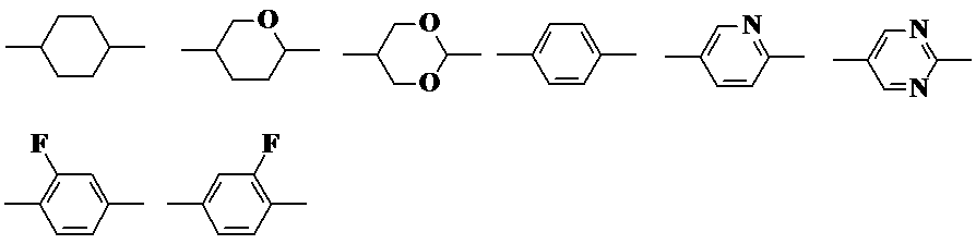

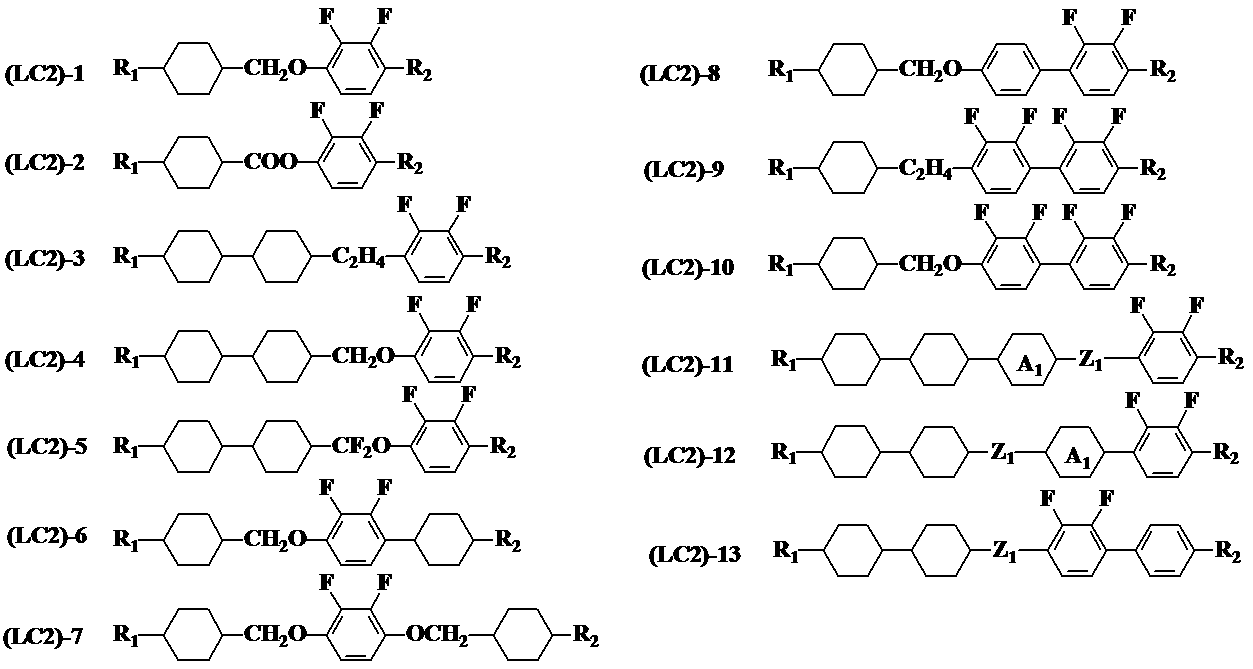
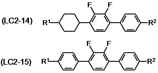
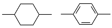


重合性化合物は、ベンゼン誘導体、トリフェニレン誘導体、トルキセン誘導体、フタロシアニン誘導体又はシクロヘキサン誘導体を分子の中心の母核とし、直鎖のアルキル基、直鎖のアルコキシ基又は置換ベンゾイルオキシ基がその側鎖として放射状に置換した構造である円盤状液晶化合物であるのが好ましい。
具体的には重合性化合物が一般式(PC1)

より好ましくは、一般式(PC1)においてMGが以下の構造
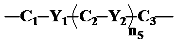
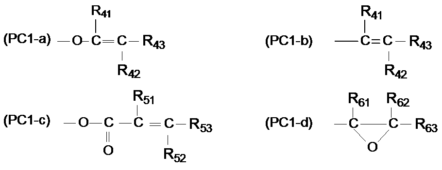
より具体的には、一般式(PC1)は一般式(PC1)-1又は一般式(PC1)-2
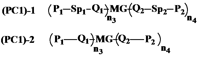
より具体的には、一般式(PC1)が一般式(PC1)-3から一般式(PC1)-11


一般式(PC1)及び一般式(PC1)-1から一般式(PC1)-11においてSp1、Sp2、Q1、及びQ2は単結合であるのが好ましい。n3+n4は1~3が好ましく、1又は2が好ましい。P1及びP2は式(7-b)であるのが好ましい。W1はF、CF3、OCF3、CH3又はOCH3であるのが好ましい。n6は1、2、3又は4である。
具体的には次に記載する化合物が好ましい。
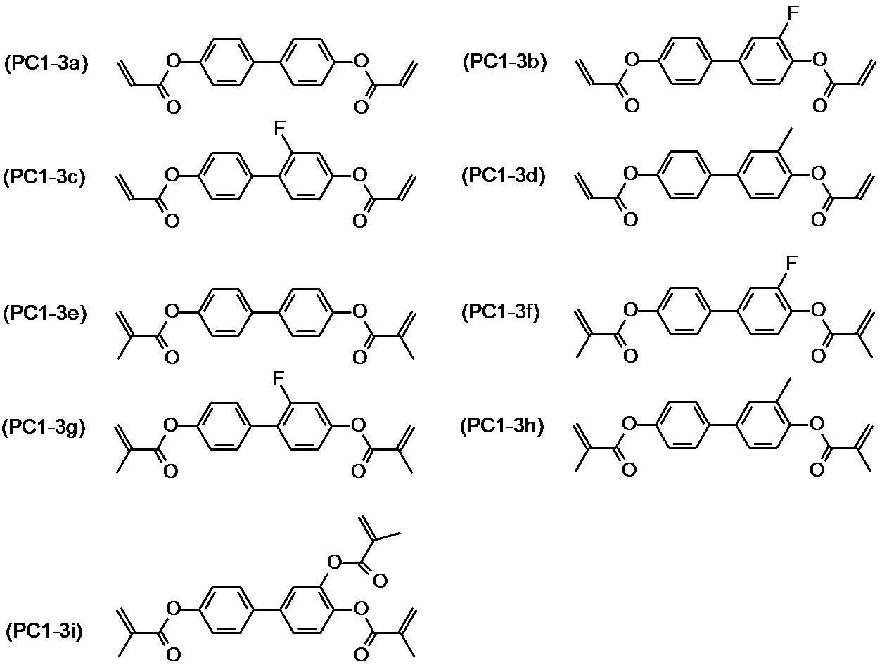
また、一般式(PC1)におけるMGが一般式(PC1)-9で表される円盤状液晶化合物

前記液晶組成物は前記用途に単独で使用することもでき、さらに酸化防止剤を1種又は2種以上含有することもでき、さらにUV吸収剤を1種又は2種以上含有することもできる。
本発明におけるカラーフィルタは、ブラックマトリックス及び少なくともRGB三色画素部から構成されるが、RGB三色画素部は、色材として、G画素部中にAl、Si、Sc、Ti、V、Mg、Fe、Co、Ni、Zn、Ga、Ge、Y、Zr、Nb、In、Sn及びPbからなる群から選ばれる金属を中心金属として有するハロゲン化金属フタロシアニン顔料であり、その中心金属が三価の場合には、その中心金属には1つのハロゲン原子、水酸基又はスルホン酸基のいずれかが結合しているか、又はオキソ又はチオ架橋しており、その中心金属が四価金属の場合には、その中心金属には1つの酸素原子又は同一でも異なっていても良い2つのハロゲン原子、水酸基又はスルホン酸基のいずれかが結合しているハロゲン化金属フタロシアニン顔料を含有する。また、RGB三色画素部は、色材として、R画素部中にジケトピロロピロール顔料及び/又はアニオン性赤色有機染料を、B画素部中にε型銅フタロシニアン顔料及び/又はカチオン性青色有機染料を含有するのが好ましい。
G画素部中の上記ハロゲン化金属フタロシアニン顔料としては、次の2つの群のハロゲン化金属フタロシアニン顔料が挙げられる。
Al、Si、Sc、Ti、V、Mg、Fe、Co、Ni、Zn、Ga、Ge、Y、Zr、Nb、In、Sn及びPbからなる群から選ばれる金属を中心金属として有し、フタロシアニン分子1個当たり8~16個のハロゲン原子がフタロシアニン分子のベンゼン環に結合したハロゲン化金属フタロシアニン顔料であり、その中心金属が三価の場合には、その中心金属には1つのハロゲン原子、水酸基又はスルホン酸基(-SO3H)のいずれかが結合しており、中心金属が四価金属の場合には、その中心金属には1つの酸素原子又は同一でも異なっていても良い2つのハロゲン原子、水酸基又はスルホン酸基のいずれかが結合しているハロゲン化金属フタロシアニン顔料。
Al、Sc、Ga、Y及びInからなる群から選ばれる三価金属を中心金属とし、フタロシアニン分子1個当たり8~16個のハロゲン原子がフタロシアニン分子のベンゼン環に結合したハロゲン化金属フタロシアニンの2分子を構成単位とし、これら構成単位の各中心金属が酸素原子、硫黄原子、スルフィニル(-SO-)及びスルホニル(-SO2-)からなる群から選ばれる二価原子団を介して結合したハロゲン化金属フタロシアニン二量体からなる顔料。
本発明で用いるハロゲン化金属フタロシアニン顔料において、ベンゼン環に結合するハロゲン原子は、全て同一であっても、それぞれ異なっていてもよい。また、ひとつのベンゼン環に異なるハロゲン原子が結合していてもよい。
ここで、フタロシアニン分子1個当たり8~16個のハロゲン原子のうち9~15個の臭素原子がフタロシアニン分子のベンゼン環に結合した、本発明で用いるハロゲン化金属フタロシアニン顔料は、黄味を帯びた明るい緑色を呈し、カラーフィルタの緑色画素部への使用に最適である。本発明で用いるハロゲン化金属フタロシアニン顔料は、水や有機溶媒に不溶または難溶である。本発明で用いるハロゲン化金属フタロシアニン顔料には、後述する仕上げ処理が行われていない顔料(粗顔料とも呼ばれる)も、仕上げ処理が行われた顔料も、いずれも包含される。
前記第一群および第二群に属するハロゲン化金属フタロシアニン顔料は、下記一般式(PIG-1)で表すことが出来る。
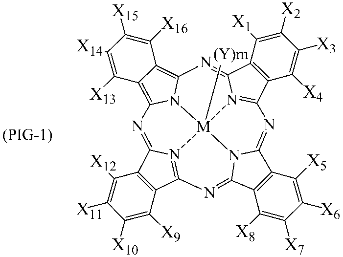
一般式(PIG-1)において、X1~X16は、水素原子、塩素原子、臭素原子またはヨウ素原子を表す。ひとつのベンゼン環に結合した4個のXの原子は同一でも異なっていても良い。4個のベンゼン環に結合したX1~X16のうち、8~16個は塩素原子、臭素原子またはヨウ素原子である。Mは中心金属を表す。後述するY及びそれの個数mが同一であるハロゲン化金属フタロシアニン顔料の範囲において、16個のX1~X16のうち塩素原子、臭素原子及びヨウ素原子の合計が8未満の顔料は青色であり、同様に16個のX1~X16のうち塩素原子、臭素原子及びヨウ素原子の合計が8以上の顔料で前記合計値が大きいほど黄味が強くなる。中心金属Mに結合するYはフッ素、塩素、臭素またはヨウ素のいずれかのハロゲン原子、酸素原子、水酸基及びスルホン酸基からなる群から選ばれる一価原子団であり、mは中心金属Mに結合するYの数を表し、0~2の整数である。
中心金属Mの原子価により、mの値が決定される。中心金属Mが、Al、Sc、Ga、Y、Inの様に原子価が3価の場合、m=1であり、フッ素、塩素、臭素、ヨウ素、水酸基及びスルホン酸基からなる群から選ばれる基の一つが中心金属に結合する。中心金属Mが、Si、Ti、V、Ge、Zr、Snの様に原子価が4価の場合は、m=2であり、酸素の一つが中心金属に結合するか、またはフッ素、塩素、臭素、ヨウ素、水酸基及びスルホン酸基からなる群から選ばれる基の二つが中心金属に結合する。中心金属Mが、Mg、Fe、Co、Ni、Zn、Zr、Sn、Pbの様に原子価が2価の場合は、Yは存在しない。
前記一般式(PIG-1)において、X1~X16については、前記定義と同義であり、中心金属MはAl、Sc、Ga、Y及びInからなる群から選ばれる三価金属を表し、mは1を表す。Yは次の原子団を表す。
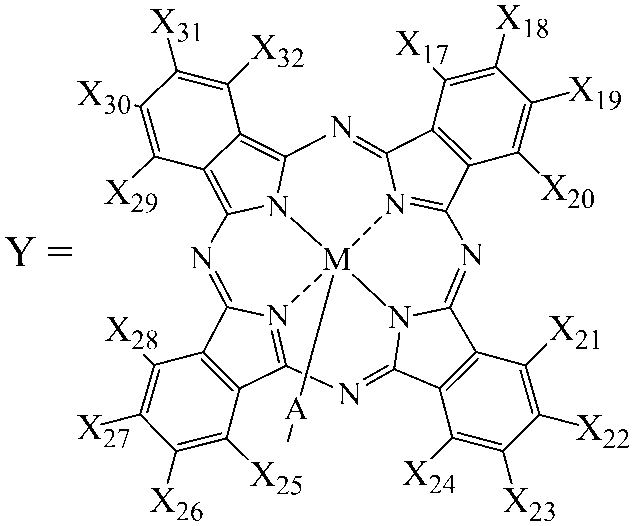
即ち、第二群に属するハロゲン化金属フタロシアニン顔料は、ハロゲン化金属フタロシアニンの2分子を構成単位とし、これらが前記二価原子団を介して結合したハロゲン化金属フタロシアニン二量体である。
(1) ハロゲン化錫フタロシアニン顔料、ハロゲン化ニッケルフタロシアニン顔料、ハロゲン化亜鉛フタロシアニン顔料の様な、Mg、Fe、Co、Ni、Zn、Zr、Sn及びPbからなる群から選ばれる二価金属を中心金属として有し、かつフタロシアニン分子1個当たり4個のベンゼン環に8~16個のハロゲン原子が結合したハロゲン化金属フタロシアニン顔料。なお、この中で、塩素化臭素化亜鉛フタロシアニン顔料は、C.I.Pigment Green 58であり、特に好ましい。
(2) ハロゲン化クロロアルミニウムフタロシアニンの様な、Al、Sc、Ga、Y及びInからなる群から選ばれる三価金属を中心金属として有し、中心金属には1つのハロゲン原子、水酸基又はスルホン酸基のいずれかを有し、かつフタロシアニン分子1個当たり4個のベンゼン環に8~16個のハロゲン原子が結合したハロゲン化金属フタロシアニン顔料。
(3) ハロゲン化オキシチタニウムフタロシアニン、ハロゲン化オキシバナジウムフタロシアニンの様な、Si、Ti、V、Ge、Zr及びSnからなる群から選ばれる四価金属を中心金属として有し、中心金属には1つの酸素原子又は同一でも異なっていても良い2つのハロゲン原子、水酸基又はスルホン酸基のいずれかを有し、かつフタロシアニン分子1個当たり4個のベンゼン環に8~16個のハロゲン原子が結合したハロゲン化金属フタロシアニン顔料。
(4) ハロゲン化されたμ-オキソ-アルミニウムフタロシアニン二量体、ハロゲン化されたμ-チオ-アルミニウムフタロシアニン二量体の様な、Al、Sc、Ga、Y及びInからなる群から選ばれる三価金属を中心金属とし、フタロシアニン分子1個当たり4個のベンゼン環に8~16個のハロゲン原子が結合したハロゲン化金属フタロシアニンの2分子を構成単位とし、これら構成単位の各中心金属が酸素原子、硫黄原子、スルフィニル及びスルホニルからなる群から選ばれる二価原子団を介して結合したハロゲン化金属フタロシアニン二量体からなる顔料。
R画素部中には、ジケトピロロピロール顔料及び/又はアニオン性赤色有機染料を含有するのが好ましい。ジケトピロロピロール顔料としては、具体的にはC.I.Pigment Red 254、同255、同264、同272、Orange 71、同73が好ましく、Red 254、同255、同264、同272がより好ましく、C.I.Pigment Red 254が特に好ましい。アニオン性赤色有機染料としては、具体的には、C.I.Solvent Red 124、Acid Red 52、同289が好ましく、C.I.Solvent Red 124が特に好ましい。
B画素部中には、ε型銅フタロシニアン顔料及び/又はカチオン性青色有機染料を含有するのが好ましい。ε型銅フタロシニアン顔料は、C.I.Pigment Blue 15:6である。カチオン性青色有機染料としては、具体的には、C.I.Solvent Blue 2、同3、同4、同5、同6、同7、同23、同43、同72、同124、C.I.Basic Blue 7、同26が好ましく、C.I.Solvent Blue 7、Basic Blue 7がより好ましく、C.I.Solvent Blue 7が特に好ましい。
また、前記RGB三色画素部は、色材として、R画素部中にC.I.Pigment Red 254を、G画素部中にAl、Si、Sc、Ti、V、Mg、Fe、Co、Ni、Zn、Ga、Ge、Y、Zr、Nb、In、Sn及びPbからなる群から選ばれる金属を中心金属として有するハロゲン化金属フタロシアニン顔料であり、その中心金属が三価の場合には、その中心金属には1つのハロゲン原子、水酸基又はスルホン酸基のいずれかが結合しているか、又はオキソ又はチオ架橋しており、中心金属が四価金属の場合には、その中心金属には1つの酸素原子又は同一でも異なっていても良い2つのハロゲン原子、水酸基又はスルホン酸基のいずれかが結合しているハロゲン化金属フタロシアニン顔料を、B画素部中にC.I.Pigment Blue 15:6を含有するのも好ましい。
前記RGB三色画素部は、色材として、G画素部中に更に、C.I.Pigment Yellow 150、同215、同185、同138、C.I.Solvent Yellow 21、同82、同83:1、同33からなる群から選ばれる少なくとも1種の有機染顔料を含有するのが好ましい。
前記RGB三色画素部は、色材として、B画素部中に更に、C.I.Pigment Blue 1、C.I.Pigment Violet 23、C.I.Basic Blue 7、C.I.Basic Violet 10、C.I.Acid Blue 1、同90、同83、C.I.Direct Blue 86からなる群から選ばれる少なくとも1種の有機染顔料を含有するのが好ましい。
R画素、G画素、B画素、必要に応じてY画素等の他の色の画素ごとに、後記する光硬化性組成物を調製して、前記した操作を繰り返すことにより、所定の位置にR画素、G画素、B画素、Y画素の着色画素部を有するカラーフィルタを製造することができる。
後記する光硬化性組成物をガラス等の透明基板上に塗布する方法としては、例えば、スピンコート法、スリットコート法、ロールコート法、インクジェット法等が挙げられる。
透明基板に塗布した光硬化性組成物の塗膜の乾燥条件は、各成分の種類、配合割合等によっても異なるが、通常、50~150℃で、1~15分間程度である。また、光硬化性組成物の光硬化に用いる光としては、200~500nmの波長範囲の紫外線、あるいは可視光を使用するのが好ましい。この波長範囲の光を発する各種光源が使用できる。
現像方法としては、例えば、液盛り法、ディッピング法、スプレー法等が挙げられる。光硬化性組成物の露光、現像の後に、必要な色の画素部が形成された透明基板は水洗いし乾燥させる。こうして得られたカラーフィルタは、ホットプレート、オーブン等の加熱装置により、90~280℃で、所定時間加熱処理(ポストベーク)することによって、着色塗膜中の揮発性成分を除去すると同時に、光硬化性組成物の硬化着色皮膜中に残存する未反応の光硬化性化合物が熱硬化し、カラーフィルタが完成する。
前記光硬化性組成物の製造方法としては、本発明のカラーフィルタ用染料及び/又は顔料組成物と、有機溶剤と分散剤とを必須成分として使用し、これらを混合し均一となる様に攪拌分散を行って、まずカラーフィルタの画素部を形成するための顔料分散液を調製してから、そこに、光硬化性化合物と、必要に応じて熱可塑性樹脂や光重合開始剤等を加えて前記光硬化性組成物とする方法が一般的である。
光硬化性組成物の調製に使用する熱可塑性樹脂としては、例えば、ウレタン系樹脂、アクリル系樹脂、ポリアミド系樹脂、ポリイミド系樹脂、スチレンマレイン酸系樹脂、スチレン無水マレイン酸系樹脂等が挙げられる。
光硬化性化合物としては、例えば、1,6-ヘキサンジオールジアクリレート、エチレングリコールジアクリレート、ネオペンチルグリコールジアクリレート、トリエチレングリコールジアクリレート、ビス(アクリロキシエトキシ)ビスフェノールA、3-メチルペンタンジオールジアクリレート等のような2官能モノマー、トリメチルロールプロパトントリアクリレート、ペンタエリスリトールトリアクリレート、トリス〔2-(メタ)アクリロイルオキシエチル)イソシアヌレート、ジペンタエリスリトールヘキサアクリレート、ジペンタエリスリトールペンタアクリレート等の比較的分子量の小さな多官能モノマー、ポリエステルアクリレート、ポリウレタンアクリレート、ポリエーテルアクリレート等の様な比較的分子量の大きな多官能モノマーが挙げられる。
また上記光重合開始剤に公知慣用の光増感剤を併用することもできる。光増感剤としては、たとえば、アミン類、尿素類、硫黄原子を有する化合物、燐原子を有する化合物、塩素原子を有する化合物またはニトリル類もしくはその他の窒素原子を有する化合物等が挙げられる。これらは、単独で用いることも、2種以上を組み合わせて用いることもできる。
前記した様な各材料を使用して、質量基準で、本発明のカラーフィルタ用染料及び/又は顔料組成物100部当たり、300~1000部の有機溶剤と、1~100部の分散剤とを、均一となる様に攪拌分散して前記染顔料液を得ることができる。次いでこの顔料分散液に、本発明のカラーフィルタ用顔料組成物1部当たり、熱可塑性樹脂と光硬化性化合物の合計が3~20部、光硬化性化合物1部当たり0.05~3部の光重合開始剤と、必要に応じてさらに有機溶剤を添加し、均一となる様に攪拌分散してカラーフィルタ画素部を形成するための光硬化性組成物を得ることができる。
現像液としては、公知慣用の有機溶剤やアルカリ水溶液を使用することができる。特に前記光硬化性組成物に、熱可塑性樹脂または光硬化性化合物が含まれており、これらの少なくとも一方が酸価を有し、アルカリ可溶性を呈する場合には、アルカリ水溶液での洗浄がカラーフィルタ画素部の形成に効果的である。
フォトリソグラフィー法によるカラーフィルタ画素部の製造方法について詳記したが、本発明のカラーフィルタ用顔料組成物を使用して調製されたカラーフィタ画素部は、その他の電着法、転写法、ミセル電解法、PVED(PhotovoltaicElectrodeposition)法、インクジェット法、反転印刷法、熱硬化法等の方法で各色画素部を形成して、カラーフィルタを製造してもよい。
本発明の液晶表示装置において、第一の基板と、第二の基板上の液晶組成物と接する面には液晶組成物を配向させるため、配向膜を必要とする液晶表示装置においてはカラーフィルタと液晶層間に配置するものであるが、配向膜の膜厚が厚いものでも100nm以下と薄く、カラーフィルタを構成する顔料等の色素と液晶層を構成する液晶化合物との相互作用を完全に遮断するものでは無い。
又、配向膜を用いない液晶表示装置においては、カラーフィルタを構成する顔料等の色素と液晶層を構成する液晶化合物との相互作用はより大きくなる。
配向膜材料としては、カルコン、シンナメート、シンナモイル又はアゾ基等を化合物中に含む、材料を使用することができ、ポリイミド、ポリアミド等の材料と組み合わせて使用してもよく、この場合配向膜はラビングを用いてもよく光配向技術を用いてもよい。
配向膜は、基板上に前記配向膜材料をスピンコート法などの方法により塗布して樹脂膜を形成することが一般的であるが、一軸延伸法、ラングミュア・ブロジェット法等を用いることもできる。
本発明の液晶表示装置において、透明電極の材料としては、導電性の金属酸化物を用いることができ、金属酸化物としては酸化インジウム(In2O3)、酸化スズ(SnO2)、酸化亜鉛(ZnO)、酸化インジウムスズ(In2O3―SnO2)、酸化インジウム亜鉛(In2O3―ZnO)、ニオブ添加二酸化チタン(Ti1-xNbxO2)、フッ素ドープ酸化スズ、グラフェンナノリボン又は金属ナノワイヤー等が使用できるが、酸化亜鉛(ZnO)、酸化インジウムスズ(In2O3―SnO2)又は酸化インジウム亜鉛(In2O3―ZnO)が好ましい。これらの透明導電膜のパターニングには、フォト・エッチング法やマスクを用いる方法などを使用することができる。
液晶組成物の物性として、以下のように表す。
TN-I :ネマチック相-等方性液体相転移温度(℃)を液晶相上限温度
Δε :誘電率異方性
Δn :屈折率異方性
η :20℃における粘性(mPa・s)
dgap:セルの第一基板と第二基板のギャップ(μm)
VHR :70℃における電圧保持率(%)
(セル厚3.5μmのセルに液晶組成物を注入し、5V印加、フレームタイム200ms、パルス幅64μsの条件で測定した時の測定電圧と初期印加電圧との比を%で表した値)
ID :70℃におけるイオン密度(pC/cm2)
(セル厚3.5μmのセルに液晶組成物を注入し、MTR-1(株式会社東陽テクニカ製)で20V印加、周波数0.05Hzの条件で測定した時のイオン密度値)
末端のn(数字) CnH2n+1-
-2- -CH2CH2-
-1O- -CH2O-
-O1- -OCH2-
-On -OCnH2n+1
-1=1- -HC=CH-
-VO- -COO-
ndm- CnH2n+1-HC=CH-(CH2)m-1-
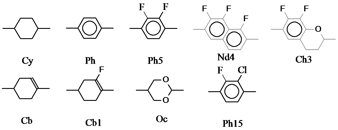
◎残像無し
○残像ごく僅かに有るも許容できるレベル
△残像有り許容できないレベル
×残像有りかなり劣悪
[着色組成物の調製]
[赤色染料着色組成物1]
赤色染料1(C.I.Solvent Red 124)10部をポリビンに入れ、プロピレングリコールモノメチルエーテルアセテート55部、0.3-0.4mmφセプルビーズを加え、ペイントコンディショナー(東洋精機株式会社製)で4時間分散した後、5μmのフィルタで濾過し染料着色液を得た。 この染料着色液75.00部とポリエステルアクリレート樹脂(アロニックス(商標名)M7100、東亜合成化学工業株式会社製)5.50部、ジぺンタエリストールヘキサアクリレート(KAYARAD(商標名)DPHA、日本化薬株式会社製)5.00部、ベンゾフェノン(KAYACURE(商標名)BP-100、日本化薬株式会社製)1.00部、ユーカーエステルEEP13.5部を分散撹拌機で撹拌し、孔径1.0μmのフィルタで濾過し、赤色染料着色組成物1を得た。
上記赤色染料着色組成物1の赤色染料1 10部に代え、赤色染料1(C.I.Solvent Red 124)8部と黄色染料1(C.I.Solvent Yellow 21)2部を用いて、上記と同様にして、赤色染料着色組成物2を得た。
上記赤色染料着色組成物1の赤色染料1 10部に代え、赤色染料2(C.I.Solvent Red 1)10部を用いて、上記と同様にして、赤色染料着色組成物3を得た。
上記赤色顔料着色組成物1の赤色顔料1 10部に代え、緑色染料1(C.I.Solvent Green 7)10部を用いて、上記と同様にして、緑色染料着色組成物1を得た。
上記赤色染料着色組成物1の赤色染料1 10部に代え、青色染料1(C.I.Solvent Blue 7)10部を用いて、上記と同様にして、青色染料着色組成物1を得た。
上記青色染料着色組成物1の青色染料1 10部に代え、青色染料1(C.I.Solvent Blue 7)7部、紫色染料1(C.I.Basic Violet 10)3部を用いて、上記と同様にして、青色染料着色組成物2を得た。
上記青色染料着色組成物2の青色染料1 7部、紫色染料1 3部に代え、青色染料2(C.I.Solvent Blue 12)10部を用いて、上記と同様にして、青色染料着色組成物3を得た。
上記赤色染料着色組成物1の赤色染料1 10部に代え、黄色染料1(C.I.Solvent Yellow 21)10部を用いて、上記と同様にして、黄色染料着色組成物1を得た。
上記黄色染料着色組成物1の黄色染料1 10部に代え、黄色染料4(C.I.Solvent Yellow 2)10部を用いて、上記と同様にして、黄色染料着色組成物2を得た。
赤色顔料1(C.I.PigmentRed254、BASF社製「IRGAPHOR RED BT-CF」)10部をポリビンに入れ、プロピレングリコールモノメチルエーテルアセテート55部、ディスパービックLPN21116(ビックケミー株式会社製)7.0部、Saint-Gobain社製0.3-0.4mmφジルコニアビーズ「ER-120S」を加え、ペイントコンディショナー(東洋精機株式会社製)で4時間分散した後、1μmのフィルタで濾過し顔料分散液を得た。
この顔料分散液75.00部とポリエステルアクリレート樹脂(アロニックス(商標名)M7100、東亜合成化学工業株式会社製)5.50部、ジぺンタエリストールヘキサアクリレート(KAYARAD(商標名)DPHA、日本化薬株式会社製)5.00部、ベンゾフェノン(KAYACURE(商標名)BP-100、日本化薬株式会社製)1.00部、ユーカーエステルEEP13.5部を分散撹拌機で撹拌し、孔径1.0μmのフィルタで濾過し、赤色顔料着色組成物1を得た。
上記赤色顔料着色組成物1の赤色顔料1 10部に代え、赤色顔料1 6部と赤色顔料2(C.I.Pigment Red 177 DIC株式会社製FASTOGEN SUPER RED ATY-TR)2部、黄色顔料2(C.I.Pigment Yellow 139)2部を用いて、上記と同様にして、赤色顔料着色組成物2を得た。
上記赤色顔料着色組成物1の赤色顔料1 10部に代え、緑色顔料1(ハロゲン化アルミニウムフタロシアニン(AlClPcBr14ClH))10部を用いて、上記と同様にして、緑色願料着色組成物1を得た。
上記緑色顔料着色組成物1の緑色顔料1 10部に代え、緑色顔料2(ハロゲン化亜鉛フタロシアニン(ZnPcBr14ClH))10部を用いて、上記と同様にして、緑色願料着色組成物2を得た。
上記緑色顔料着色組成物1の緑色顔料1 10部に代え、緑色顔料3(C.I.Pigment Green 58 DIC株式会社製FASTOGEN GREEN A110)6部と黄色顔料1(C.I.Pigment Yellow 150、LANXESS社製FANCHON FAST YELLOW E4GN)4部を用いて、上記と同様にして、緑色顔料着色組成物3を得た。
上記緑色顔料着色組成物3の緑色顔料3 6部、黄色顔料1 4部に代え、緑色顔料4(C.I.Pigment Green 58 DIC株式会社製FASTOGEN GREEN A310)4部と黄色顔料3(C.I.Pigment YELLOW 138)6部を用いて、上記と同様にして、緑色顔料着色組成物4を得た。
上記赤色顔料着色組成物1の赤色顔料1 10部に代え、青色顔料1(C.I.Pigment Blue 15:6、DIC株式会社製「FASTOGEN BLUE EP-210」)9部と紫色顔料1(C.I.Pigment VIOLET 23)1部を用いて、上記と同様にして、青色顔料着色組成物1を得た。
上記青色顔料着色組成物1の紫色顔料1に代え、紫色染料1(C.I.Basic Violet 10)1部を用いて、上記と同様にして、青色顔料染料着色組成物2を得た。
上記赤色顔料着色組成物1の赤色顔料1 10部に代え、黄色顔料1(C.I.Pigment Yellow 150、LANXESS社製FANCHON FAST YELLOW E4GN)10部を用いて、上記と同様にして、黄色顔料着色組成物1を得た。
予めブラックマトリックスが形成されてあるガラス基板に、赤色着色組成物をスピンコートにより膜厚2μmとなるように塗布した。70℃で20分間乾燥の後、超高圧水銀ランプを備えた露光機にて紫外線をフォトマスクを介してストライプ状のパターン露光をした。アルカリ現像液にて90秒間スプレー現像、イオン交換水で洗浄し、風乾した。さらに、クリーンオーブン中で、230℃で30分間ポストベークを行い、ストライプ状の着色層である赤色画素を透明基板上に形成した。
次に、緑色着色組成物も同様にスピンコートにて膜厚が2μmとなるように塗布。乾燥後、露光機にてストライプ状の着色層を前述の赤色画素とはずらした場所に露光し現像することで、前述赤色画素と隣接した緑色画素を形成した。
次に、青色着色組成物についても同様にスピンコートにて膜厚2μmで赤色画素、緑色画素と隣接した青色画素を形成した。これで、透明基板上に赤、緑、青の3色のストライプ状の画素を持つカラーフィルタが得られた。
必要に応じて、黄色着色組成物についても、同様にスピンコートにて膜厚2μmで赤色画素、緑色画素と隣接した青色画素を形成した。これで、透明基板上に赤、緑、青、黄の4色のストライプ状の画素を持つカラーフィルタが得られた。
表1に示す染料着色組成物又は顔料着色組成物を用い、カラーフィルタ1~4及び比較カラーフィルタ1を作成した。
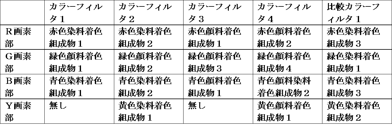
電極構造を第一及び第二の基板に作成し、各々の対向側に垂直配向性の配向膜を形成したのち弱ラビング処理を行い、VAセルを作成し、第一の基板と第二の基板の間に表2に示す負の誘電異方性を有する液晶組成物1を挟持した。次に、表1に示すカラーフィルタ1~4を用いて実施例1の液晶表示装置を作成した(dgap=3.5μm、配向膜SE-5300)。得られた液晶表示装置のVHR及びIDを測定した。また、得られた液晶表示装置の焼き付き評価を行った。その結果を表3に示す。
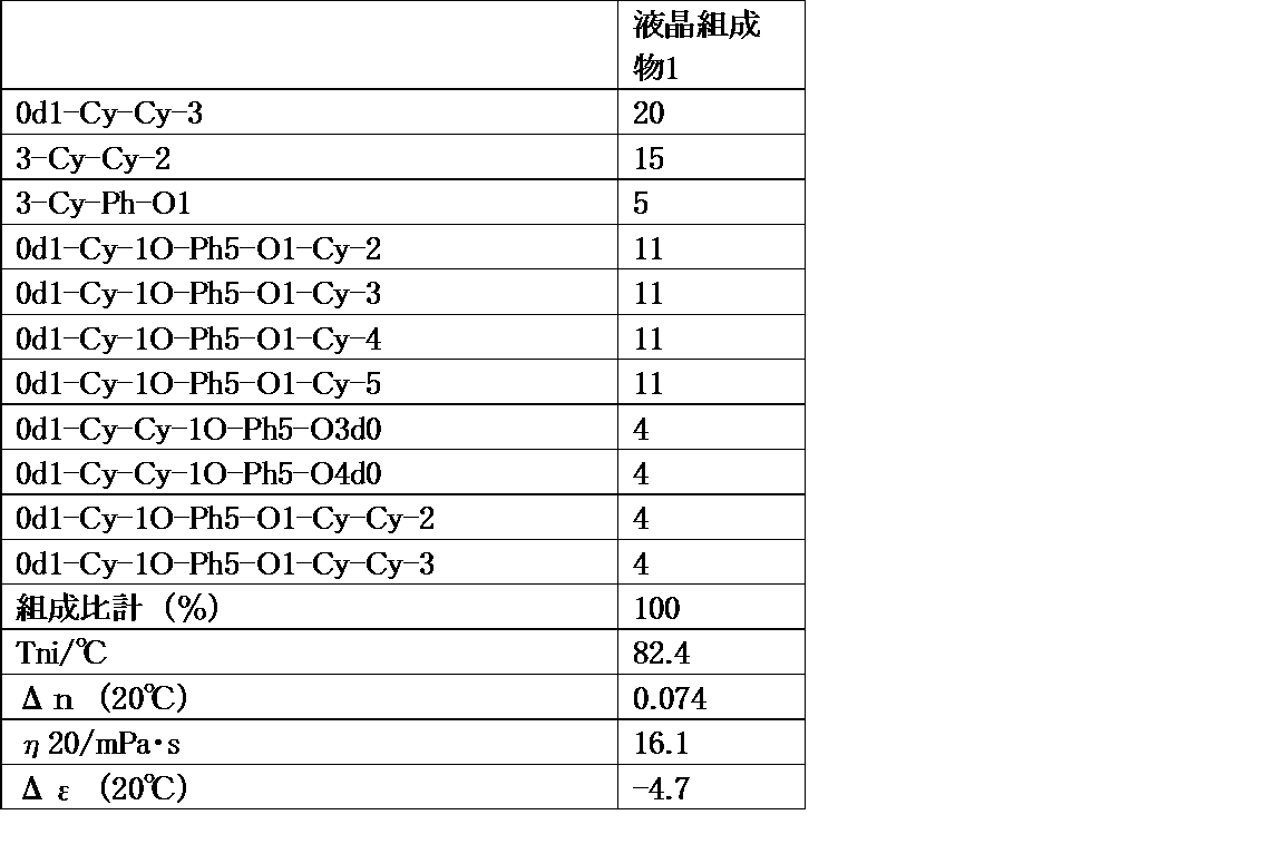

実施例1で用いたVAセルに表4に示す負の誘電異方性を有する比較液晶組成物1及び比較液晶組成物2を挟持し、表1に示すカラーフィルタ1~4を用いて比較例1~8の液晶表示装置を作製し、そのVHR及びIDを測定した。また、その液晶表示装置の焼き付き評価を行った。その結果を表5及び表6に示す。
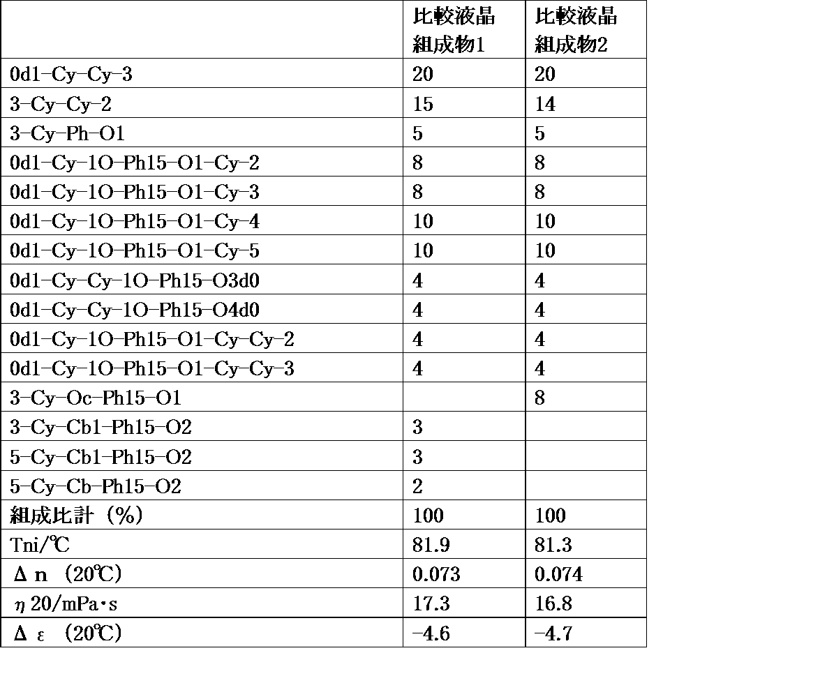
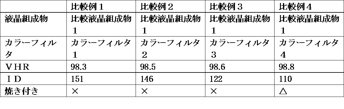

実施例1で用いたVAセルに表2に示す負の誘電異方性を有する液晶組成物1を挟持し、表1に示す比較カラーフィルタ1を用いて比較例9の液晶表示装置を作製し、そのVHR及びIDを測定した。また、その液晶表示装置の焼き付き評価を行った。その結果を表7に示す。

実施例1と同様に表8に示す負の誘電異方性を有する比較液晶組成物3を狭持し、表1に示すカラーフィルタ1~4を用いて比較例10~13の液晶表示装置を作製し、そのVHR及びIDを測定した。また、その液晶表示装置の焼き付き評価を行った。その結果を表9に示す。

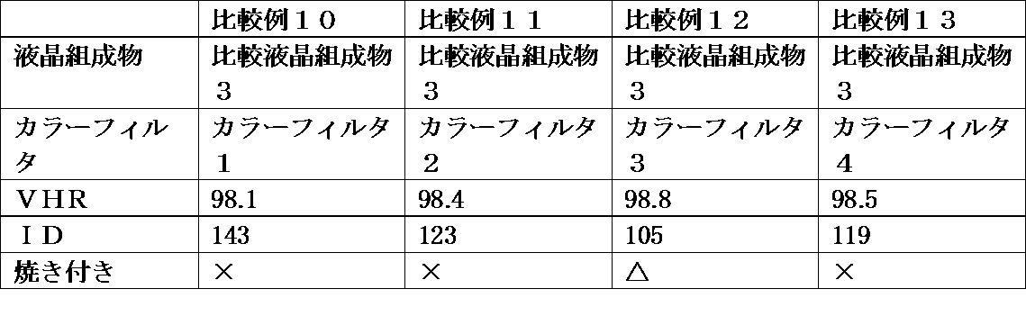
実施例1と同様に表10に示す負の誘電異方性液晶を狭持し、表1に示すカラーフィルタを用いて実施例5~12の液晶表示装置を作成し、そのVHR及びIDを測定した。また、その液晶表示装置の焼き付き評価を行った。その結果を表11及び12に示す。
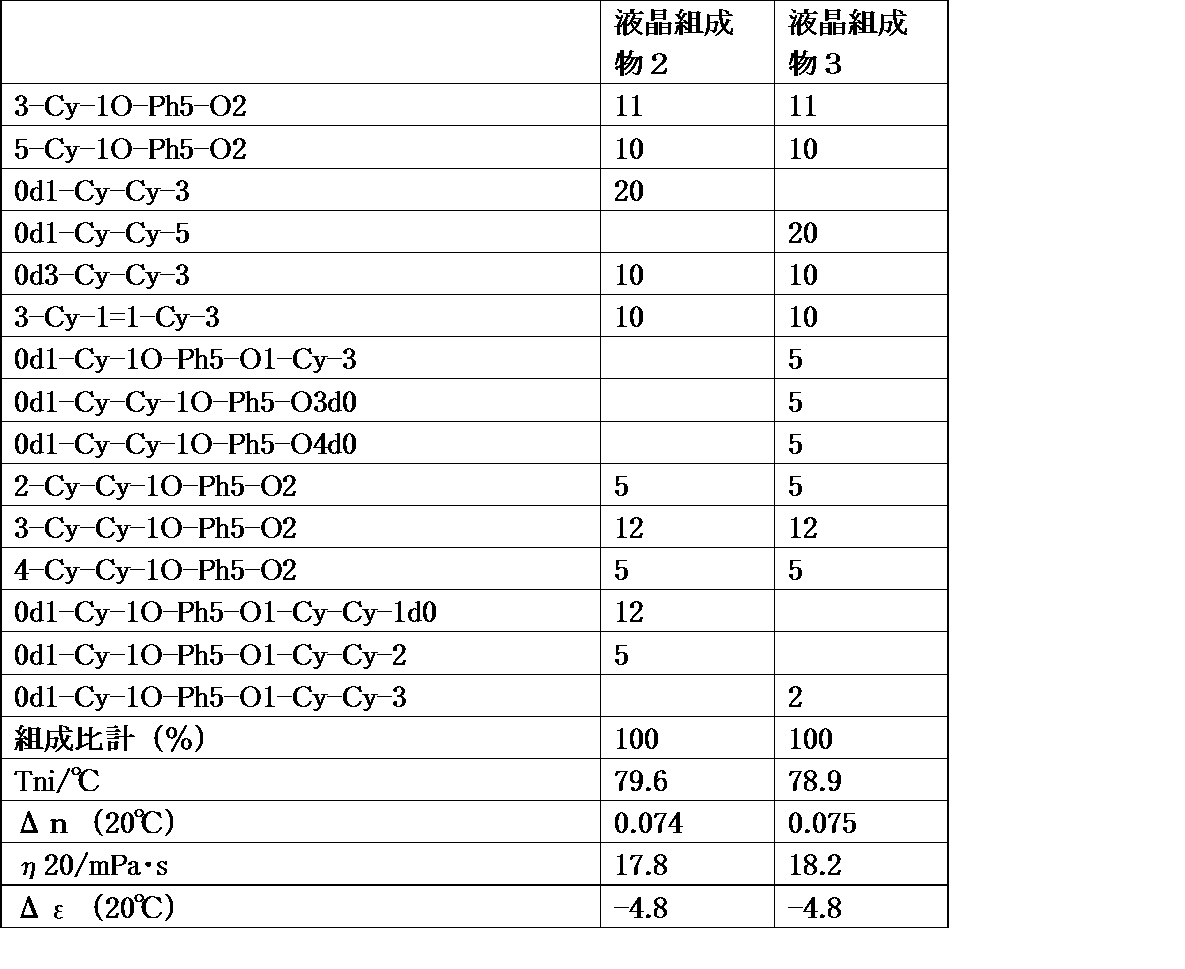

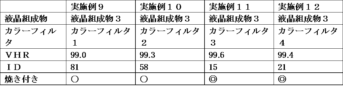
実施例1と同様に表13に示す負の誘電異方性液晶を狭持し、表1に示すカラーフィルタを用いて実施例13~28の液晶表示装置作成し、そのVHR及びIDを測定した。また、その液晶表示装置の焼き付き評価を行った。その結果を表14~17に示す。


実施例1と同様に表18に示す負の誘電異方性液晶を狭持し、表1に示すカラーフィルタを用いて実施例29~40の液晶表示装置作成し、そのVHR及びIDを測定した。また、その液晶表示装置の焼き付き評価を行った。その結果を表19~21に示す。
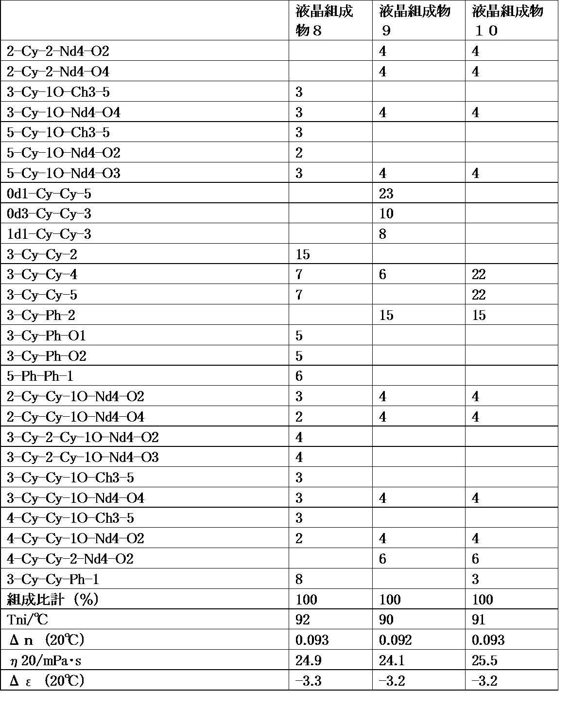

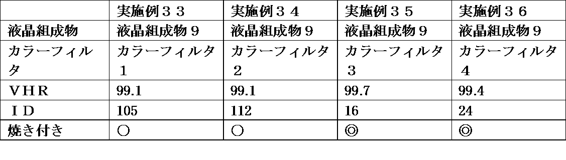

実施例1と同様に表22に示す負の誘電異方性液晶を狭持し、表1に示すカラーフィルタを用いて実施例41~48の液晶表示装置作成し、そのVHR及びIDを測定した。また、その液晶表示装置の焼き付き評価を行った。その結果を表23~24に示す。
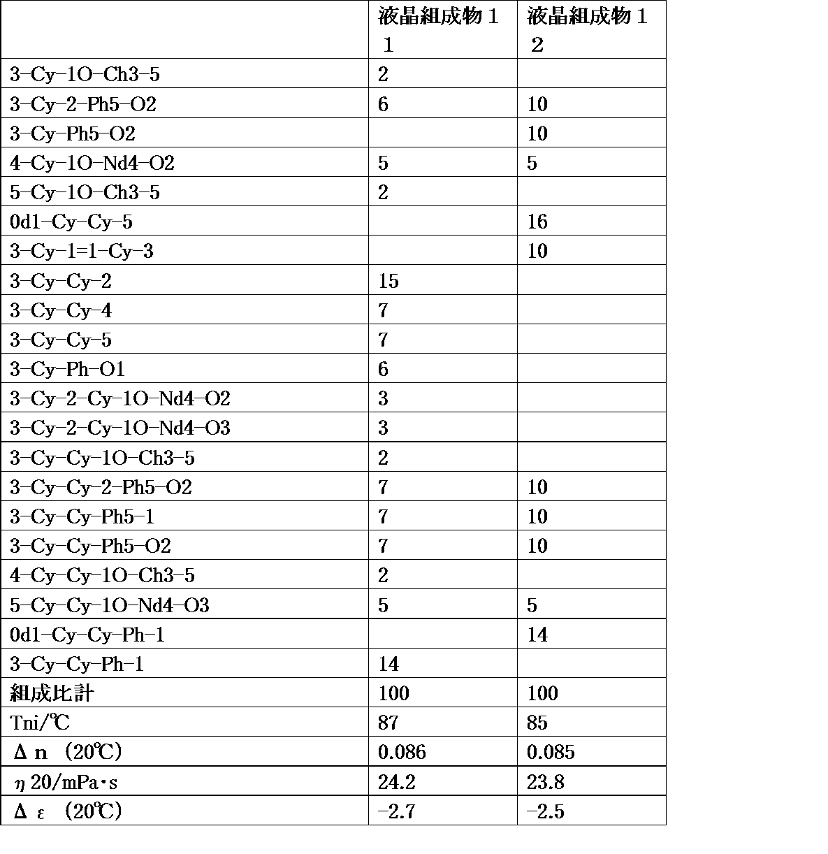
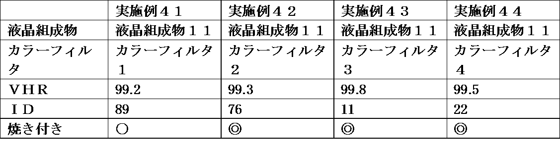

実施例1と同様に表25に示す負の誘電異方性液晶を狭持し、表1に示すカラーフィルタを用いて実施例49~60の液晶表示装置作成し、そのVHR及びIDを測定した。また、その液晶表示装置の焼き付き評価を行った。その結果を表26~28に示す。
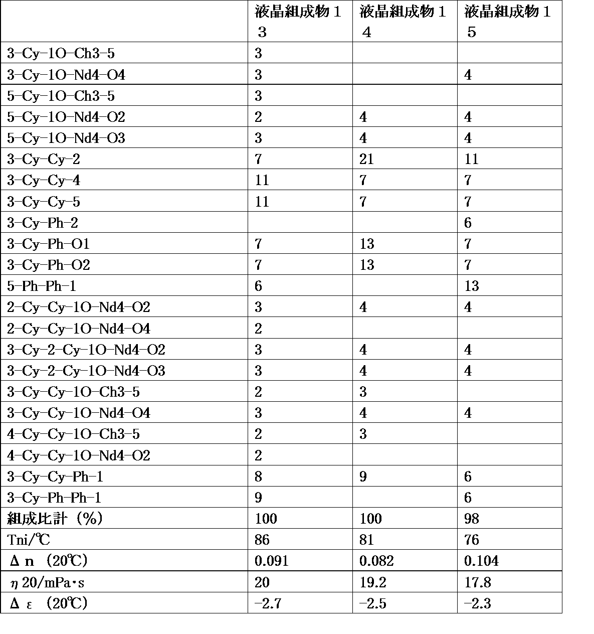
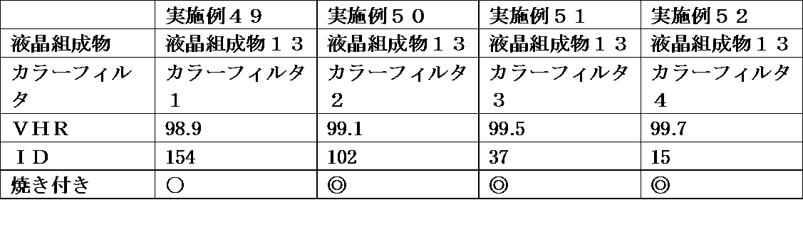

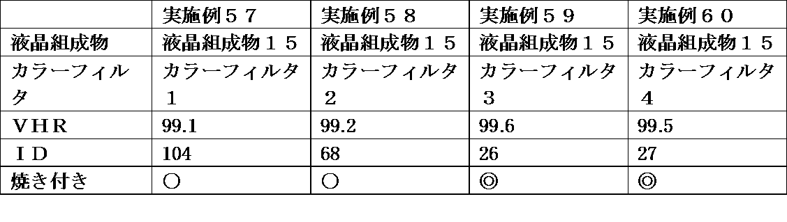
実施例1と同様に表29に示す負の誘電異方性液晶を狭持し、表1に示すカラーフィルタを用いて実施例61~76の液晶表示装置作成し、そのVHR及びIDを測定した。また、その液晶表示装置の焼き付き評価を行った。その結果を表30~33に示す。
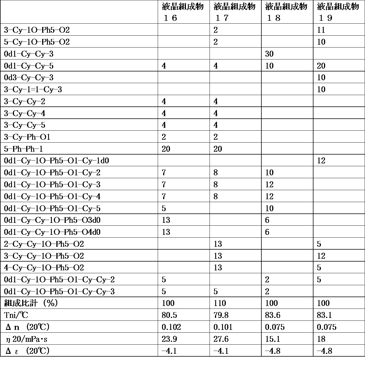


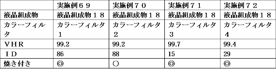

実施例1と同様に表34に示す負の誘電異方性液晶を狭持し、表1に示すカラーフィルタを用いて実施例77~92の液晶表示装置作成し、そのVHR及びIDを測定した。また、その液晶表示装置の焼き付き評価を行った。その結果を表35~38に示す。
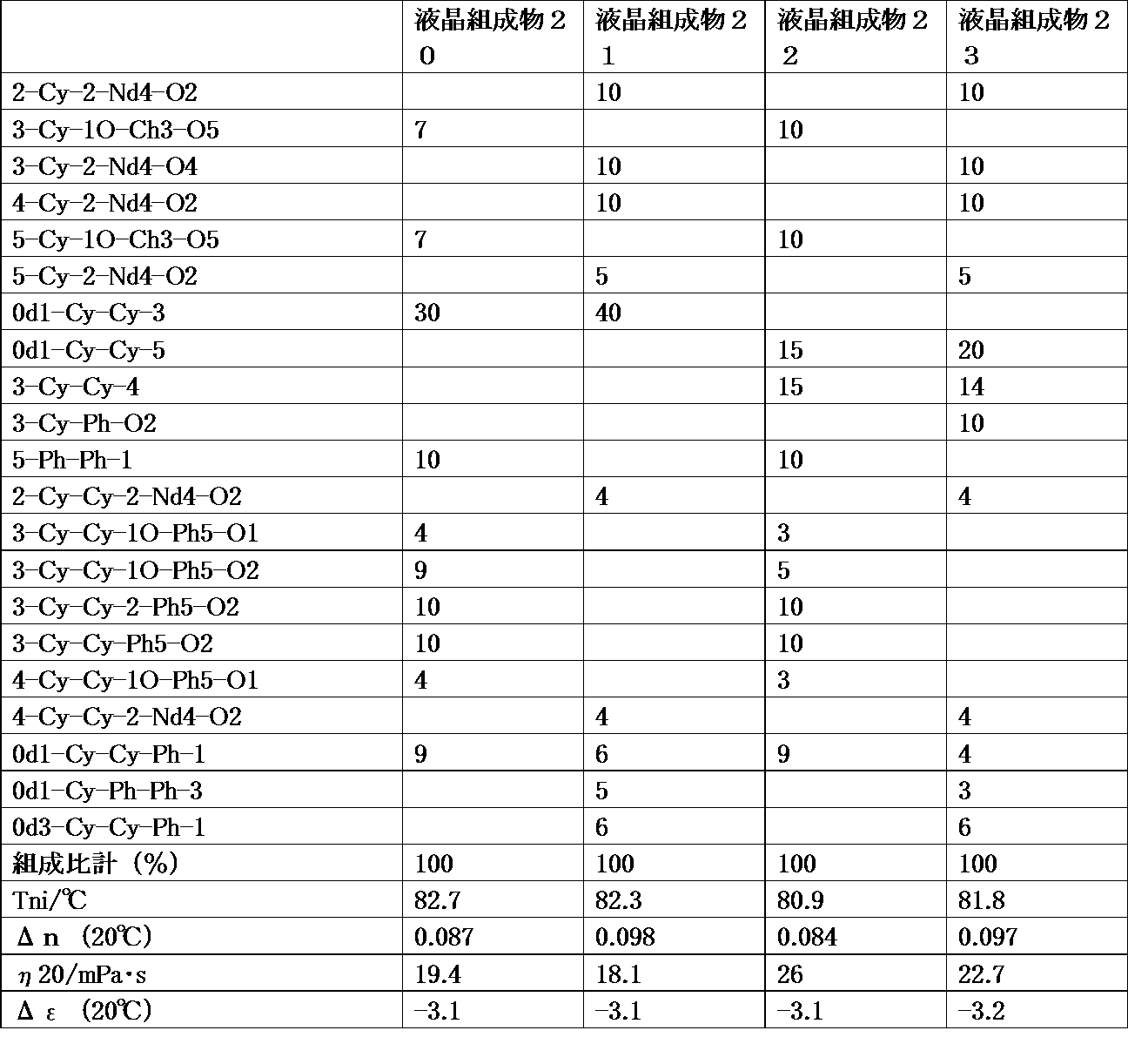


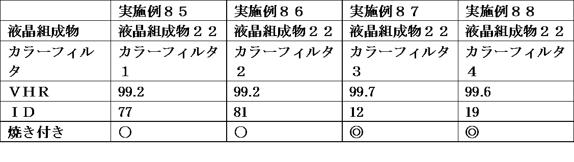
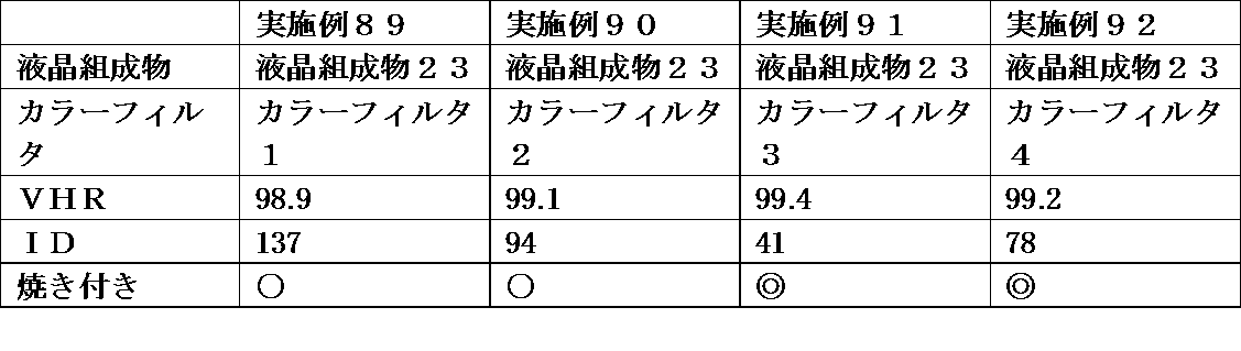
実施例1と同様に表39に示す負の誘電異方性液晶を狭持し、表1に示すカラーフィルタを用いて実施例93~100の液晶表示装置作成し、そのVHR及びIDを測定した。また、その液晶表示装置の焼き付き評価を行った。その結果を表40~41に示す。

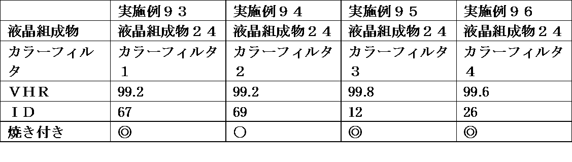
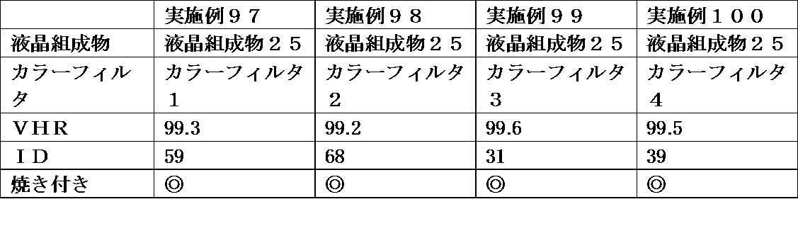
実施例1と同様に表42に示す負の誘電異方性液晶を狭持し、表1に示すカラーフィルタを用いて実施例101~112の液晶表示装置作成し、そのVHR及びIDを測定した。また、その液晶表示装置の焼き付き評価を行った。その結果を表43~45に示す。
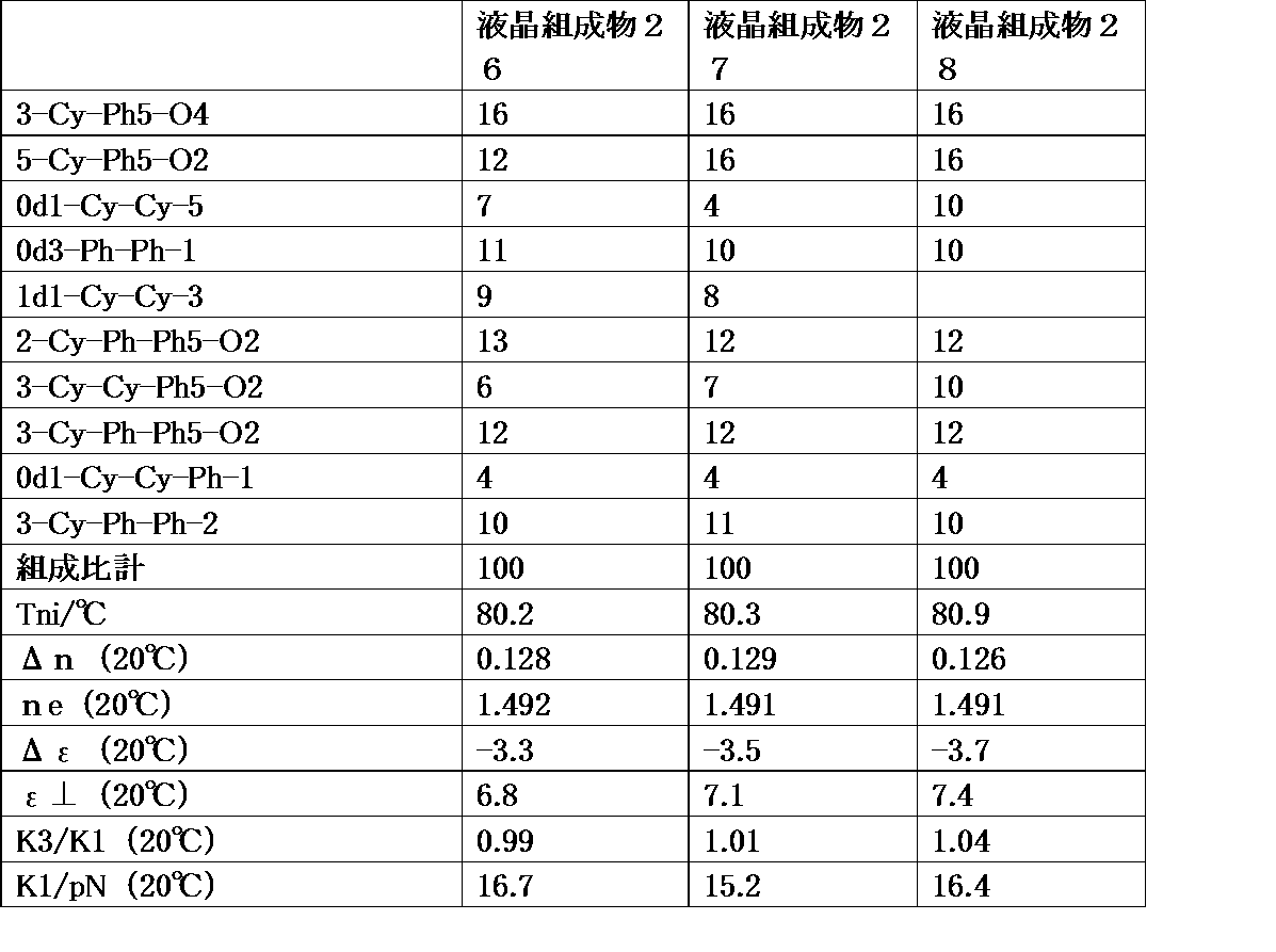
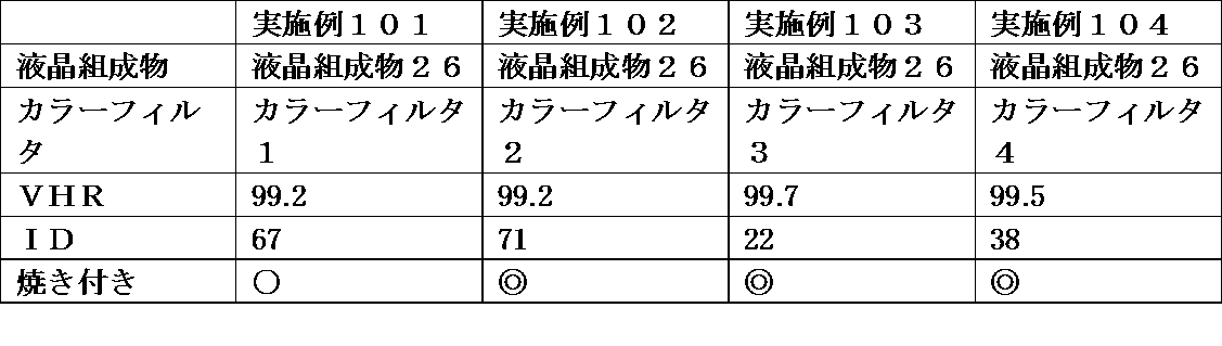


実施例1と同様に表46に示す負の誘電異方性液晶を狭持し、表1に示すカラーフィルタを用いて実施例101~112の液晶表示装置作成し、そのVHR及びIDを測定した。また、その液晶表示装置の焼き付き評価を行った。その結果を表47~49に示す。

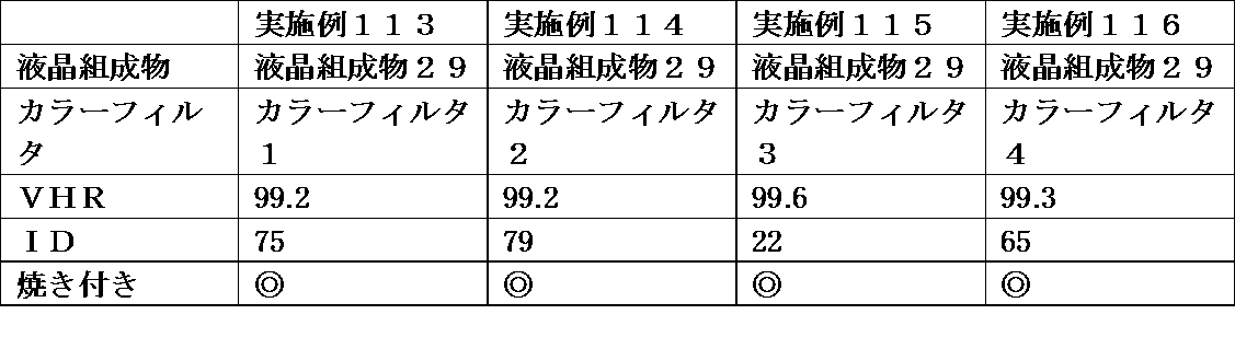
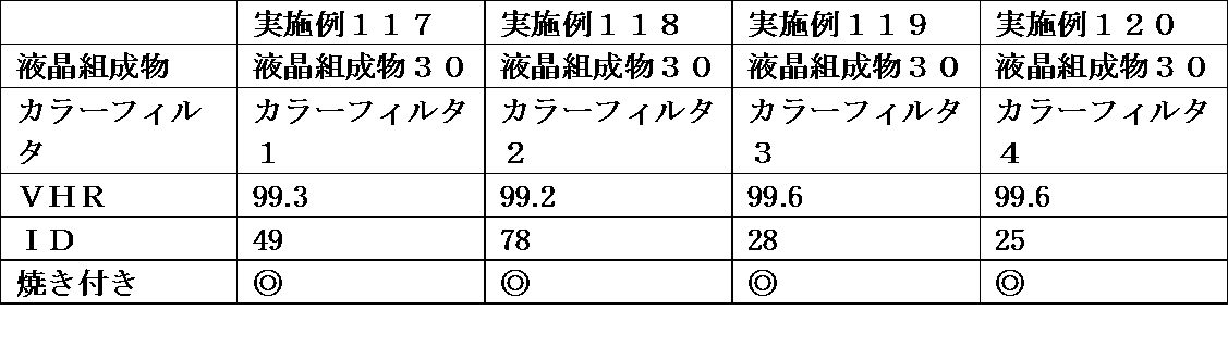
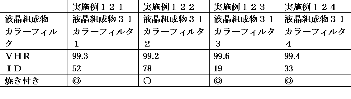
実施例1と同様に表50に示す負の誘電異方性液晶を狭持し、表1に示すカラーフィルタを用いて実施例125~128の液晶表示装置作成し、そのVHR及びIDを測定した。また、その液晶表示装置の焼き付き評価を行った。その結果を表51に示す。
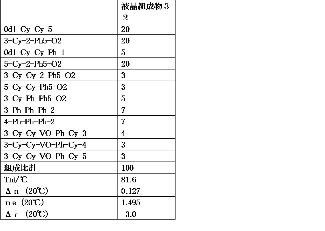

実施例1で用いた負の誘電異方性を有する液晶組成物1に2-メチル-アクリル酸4’-{2-[4-(2-アクリロイルオキシ-エチル)-フェノキシカルボニル]-エチル}-ビフェニル-4-イルエステル0.3質量%を混合し液晶組成物33とした。実施例1で用いたVAセルにこの液晶組成物33を挟持し、電極間に駆動電圧を印加したまま、紫外線を600秒間照射(3.0J/cm2)し、重合処理を行い、次に、表1に示すカラーフィルタ1~4を用いて実施例129~132の液晶表示装置を作成し、そのVHR及びIDを測定した。また、その液晶表示装置の焼き付き評価を行った。その結果を表50に示す。

負の誘電異方性を有する液晶組成物29にビスメタクリル酸ビフェニル‐4,4’‐ジイル 0.3質量%を混合し液晶組成物34とした。実施例1で用いたVAセルにこの液晶組成物30を挟持し、電極間に駆動電圧を印加したまま、紫外線を600秒間照射(3.0J/cm2)し、重合処理を行い、次に、表1に示すカラーフィルタ1~4を用いて実施例132~135の液晶表示装置を作成し、そのVHR及びIDを測定した。また、その液晶表示装置の焼き付き評価を行った。その結果を表53に示す。

負の誘電異方性を有する液晶組成物32にビスメタクリル酸 3‐フルオロビフェニル‐4,4’‐ジイル 0.3質量%を混合し液晶組成物35とした。実施例1で用いたVAセルにこの液晶組成物35を挟持し、電極間に駆動電圧を印加したまま、紫外線を600秒間照射(3.0J/cm2)し、重合処理を行い、次に、表1に示すカラーフィルタ1~4を用いて実施例136~139の液晶表示装置を作成し、そのVHR及びIDを測定した。また、その液晶表示装置の焼き付き評価を行った。その結果を表54に示す。
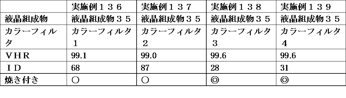
Claims (16)
- 第一の基板と、第二の基板と、前記第一の基板と第二の基板間に挟持された液晶組成物層と、ブラックマトリックス及び少なくともRGB三色画素部から構成されるカラーフィルタと、画素電極と共通電極とを備え、
前記液晶組成物層が一般式(LC1)から一般式(LC4)


前記RGB三色画素部が、色材として、G画素部中にAl、Si、Sc、Ti、V、Mg、Fe、Co、Ni、Zn、Ga、Ge、Y、Zr、Nb、In、Sn及びPbからなる群から選ばれる金属を中心金属として有するハロゲン化金属フタロシアニン顔料であり、その中心金属が三価の場合には、その中心金属には1つのハロゲン原子、水酸基又はスルホン酸基のいずれかが結合しているか、又はオキソ又はチオ架橋しており、その中心金属が四価金属の場合には、その中心金属には1つの酸素原子又は同一でも異なっていても良い2つのハロゲン原子、水酸基又はスルホン酸基のいずれかが結合しているハロゲン化金属フタロシアニン顔料を含有することを特徴とする液晶表示装置。 - 前記RGB三色画素部が、色材として、R画素部中にジケトピロロピロール顔料及び/又はアニオン性赤色有機染料を、B画素部中にε型銅フタロシニアン顔料及び/又はカチオン性青色有機染料を含有することを特徴とする請求項1記載の液晶表示装置。
- 前記RGB三色画素部が、色材として、R画素部中にC.I.Solvent Red 124を、B画素部中にC.I.Solvent Blue 7を含有することを特徴とする請求項1又は2に記載の液晶表示装置。
- 前記RGB三色画素部が、色材として、R画素部中にC.I.Pigment Red 254を、B画素部中にC.I.Pigment Blue 15:6を含有することを特徴とする請求項1又は2に記載の液晶表示装置。
- G画素部中にフタロシアニン分子1個当たり8~16個のハロゲン原子がフタロシアニン分子のベンゼン環に結合したZnを中心金属として有するハロゲン化亜鉛フタロシアニン顔料を含有する請求項1~4のいずれか一項に記載の液晶表示装置。
- G画素部中にC.I.Pigment Green 58を含有する請求項1~5のいずれか一項に記載の液晶表示装置。
- G画素部中に更に、C.I.Pigment Yellow 150、同215、同185、同138、C.I.Solvent Yellow 21、同82、同83:1、同33からなる群から選ばれる少なくとも1種の有機染顔料を含有する請求項1~6のいずれか一項に記載の液晶表示装置。
- カラーフィルタが、ブラックマトリックスとRGB三色画素部とY画素部とから構成され、色材として、Y画素部に、C.I.Pigment Yellow 150、同215、同185、同138、同139、C.I.Solvent Yellow 21、同82、同83:1、同33、同162からなる群から選ばれる少なくとも1種の黄色有機染顔料を含有する請求項1~7のいずれか一項に記載の液晶表示装置。
- 前記液晶組成物層として、一般式(LC5)


- 一般式(LC1)が下記一般式(LC1)-1から一般式(LC1)-7

- 一般式(LC2)が下記一般式(LC2)-1から一般式(LC2)-15
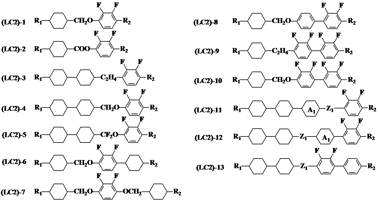


- 一般式(LC3)が下記一般式(LC3)-1から一般式(LC3)-6、一般式(LC4)が下記一般式(LC4)-1から一般式(LC4)-4
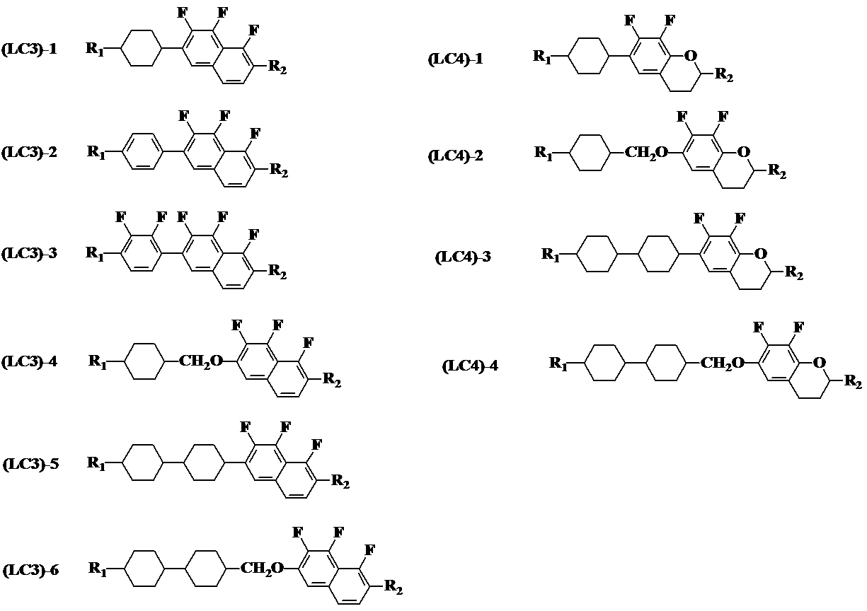
- 一般式(LC5)が一般式(LC5)-1から一般式(LC5)-13

- 前記液晶組成物層が重合性化合物を1種又は2種以上含有する液晶組成物を重合してなる重合体により構成される請求項1~13のいずれか一項に記載の液晶表示装置。
- 重合性化合物が、ベンゼン誘導体、トリフェニレン誘導体、トルキセン誘導体、フタロシアニン誘導体又はシクロヘキサン誘導体を分子の中心の母核とし、直鎖のアルキル基、直鎖のアルコキシ基又は置換ベンゾイルオキシ基がその側鎖として放射状に置換した構造である円盤状液晶化合物である請求項14記載の液晶表示装置。
- 重合性化合物が一般式(PC1)

Priority Applications (5)
| Application Number | Priority Date | Filing Date | Title |
|---|---|---|---|
| KR1020137022648A KR101370951B1 (ko) | 2012-02-01 | 2013-01-29 | 액정 표시 장치 |
| US14/115,050 US8860912B2 (en) | 2012-02-01 | 2013-01-29 | Liquid crystal display device |
| CN201380000792.6A CN103403613B (zh) | 2012-02-01 | 2013-01-29 | 液晶显示装置 |
| EP13744268.7A EP2696236B1 (en) | 2012-02-01 | 2013-01-29 | Liquid crystal display device |
| JP2013512039A JP5333880B1 (ja) | 2012-02-01 | 2013-01-29 | 液晶表示装置 |
Applications Claiming Priority (2)
| Application Number | Priority Date | Filing Date | Title |
|---|---|---|---|
| JP2012019794 | 2012-02-01 | ||
| JP2012-019794 | 2012-02-01 |
Publications (1)
| Publication Number | Publication Date |
|---|---|
| WO2013115164A1 true WO2013115164A1 (ja) | 2013-08-08 |
Family
ID=48905199
Family Applications (1)
| Application Number | Title | Priority Date | Filing Date |
|---|---|---|---|
| PCT/JP2013/051860 Ceased WO2013115164A1 (ja) | 2012-02-01 | 2013-01-29 | 液晶表示装置 |
Country Status (7)
| Country | Link |
|---|---|
| US (1) | US8860912B2 (ja) |
| EP (1) | EP2696236B1 (ja) |
| JP (1) | JP5333880B1 (ja) |
| KR (1) | KR101370951B1 (ja) |
| CN (1) | CN103403613B (ja) |
| TW (1) | TWI443387B (ja) |
| WO (1) | WO2013115164A1 (ja) |
Cited By (15)
| Publication number | Priority date | Publication date | Assignee | Title |
|---|---|---|---|---|
| WO2014041985A1 (ja) * | 2012-09-11 | 2014-03-20 | Dic株式会社 | 液晶表示装置 |
| US20140211137A1 (en) * | 2011-12-19 | 2014-07-31 | Dic Corporation | Liquid crystal display device |
| US8860912B2 (en) | 2012-02-01 | 2014-10-14 | Dic Corporation | Liquid crystal display device |
| US9334399B2 (en) | 2012-12-12 | 2016-05-10 | Cheil Industries Inc. | Photosensitive resin composition and black spacer using the same |
| US9535190B2 (en) | 2014-01-09 | 2017-01-03 | Samsung Sdi Co., Ltd. | Photosensitive resin composition and color filter using the same |
| EP2960711A4 (en) * | 2013-09-24 | 2017-01-04 | DIC Corporation | Liquid-crystal display |
| KR20170005364A (ko) * | 2015-07-02 | 2017-01-12 | 메르크 파텐트 게엠베하 | 액정 매질 |
| EP2983037A4 (en) * | 2013-09-24 | 2017-02-22 | DIC Corporation | Liquid-crystal display |
| US9683171B2 (en) | 2013-06-06 | 2017-06-20 | Dic Corporation | Liquid crystal display device |
| EP3070147A4 (en) * | 2013-11-13 | 2017-07-12 | JNC Corporation | Liquid crystal composition and liquid crystal display element |
| US10047289B2 (en) | 2013-11-12 | 2018-08-14 | Dic Corporation | Liquid crystal display device |
| US10108052B2 (en) | 2013-10-30 | 2018-10-23 | Dic Corporation | Liquid-crystal display element |
| US10414980B2 (en) | 2014-07-29 | 2019-09-17 | Dic Corporation | Liquid-crystal display |
| US10421906B2 (en) | 2014-07-29 | 2019-09-24 | Dic Corporation | Liquid-crystal display element |
| US10437107B2 (en) | 2013-10-30 | 2019-10-08 | Dic Corporation | Liquid-crystal display element |
Families Citing this family (20)
| Publication number | Priority date | Publication date | Assignee | Title |
|---|---|---|---|---|
| TWI447210B (zh) * | 2012-07-25 | 2014-08-01 | Dainippon Ink & Chemicals | Liquid crystal display device |
| TWI476273B (zh) | 2012-12-04 | 2015-03-11 | 迪愛生股份有限公司 | Liquid crystal display device |
| JP5321932B1 (ja) | 2013-02-21 | 2013-10-23 | Dic株式会社 | 液晶表示装置 |
| US9441158B2 (en) * | 2013-05-28 | 2016-09-13 | Dic Corporation | Liquid crystal display device |
| US10011773B2 (en) * | 2013-06-06 | 2018-07-03 | Dic Corporation | Liquid crystal display device |
| JP5505568B1 (ja) * | 2013-06-18 | 2014-05-28 | Dic株式会社 | 液晶表示装置 |
| WO2014203752A1 (ja) * | 2013-06-18 | 2014-12-24 | Dic株式会社 | 液晶表示装置 |
| KR101717466B1 (ko) * | 2013-11-12 | 2017-03-17 | 디아이씨 가부시끼가이샤 | 액정 표시 소자 |
| US9810938B2 (en) | 2013-11-29 | 2017-11-07 | Dic Corporation | Liquid crystal display device |
| CN105793770A (zh) * | 2013-12-11 | 2016-07-20 | Dic株式会社 | 液晶显示元件及其制造方法 |
| WO2015097740A1 (ja) * | 2013-12-24 | 2015-07-02 | Dic株式会社 | 液晶表示装置 |
| CN106104371A (zh) * | 2014-03-26 | 2016-11-09 | 住友化学株式会社 | 液晶显示装置 |
| CN106255738A (zh) * | 2014-11-25 | 2016-12-21 | 默克专利股份有限公司 | 液晶介质 |
| CN107429078B (zh) * | 2015-03-27 | 2019-10-15 | 三菱化学株式会社 | 着色树脂组合物、滤色片、以及图像显示装置 |
| KR20160139114A (ko) * | 2015-05-26 | 2016-12-07 | 삼성디스플레이 주식회사 | 표시 장치 및 표시 장치의 리페어 방법 |
| JP2017105915A (ja) * | 2015-12-09 | 2017-06-15 | Dic株式会社 | 液晶組成物及びそれを使用した液晶表示素子 |
| TWI624695B (zh) * | 2017-01-19 | 2018-05-21 | 國立交通大學 | 軟性液晶透鏡陣列 |
| JP7022558B2 (ja) | 2017-06-27 | 2022-02-18 | キヤノン株式会社 | 印刷システム、印刷装置と情報処理装置とその制御方法、及びプログラム |
| JP7114868B2 (ja) * | 2017-09-26 | 2022-08-09 | Dic株式会社 | 液晶表示装置 |
| CN109575937A (zh) * | 2018-12-01 | 2019-04-05 | 四川师范大学 | 一种吐昔烯酮-苯并菲盘状液晶化合物及其制备方法 |
Citations (7)
| Publication number | Priority date | Publication date | Assignee | Title |
|---|---|---|---|---|
| JP2000019321A (ja) | 1998-06-29 | 2000-01-21 | Toray Ind Inc | カラーフィルター用顔料、カラーペースト及びカラーフィルター |
| JP2000192040A (ja) | 1998-12-25 | 2000-07-11 | Toshiba Corp | 液晶表示装置 |
| JP2005281559A (ja) * | 2004-03-30 | 2005-10-13 | Dainippon Ink & Chem Inc | ネマチック液晶組成物及びこれを用いた液晶表示素子 |
| JP2009109542A (ja) | 2007-10-26 | 2009-05-21 | Toppan Printing Co Ltd | カラーフィルタおよびこれを備えた横電界方式の液晶表示装置 |
| JP2009163014A (ja) * | 2008-01-07 | 2009-07-23 | Toppan Printing Co Ltd | 液晶表示装置及び液晶表示装置用カラーフィルタ |
| JP2010256509A (ja) * | 2009-04-23 | 2010-11-11 | Jsr Corp | 着色組成物、カラーフィルタおよびカラー液晶表示素子 |
| WO2011092973A1 (ja) * | 2010-01-26 | 2011-08-04 | Jnc株式会社 | 液晶組成物および液晶表示素子 |
Family Cites Families (14)
| Publication number | Priority date | Publication date | Assignee | Title |
|---|---|---|---|---|
| JP4437651B2 (ja) | 2003-08-28 | 2010-03-24 | 新日鐵化学株式会社 | 感光性樹脂組成物及びそれを用いたカラーフィルター |
| KR101030538B1 (ko) * | 2004-06-17 | 2011-04-22 | 엘지디스플레이 주식회사 | Ips 모드 액정표시소자 |
| CN101133138B (zh) | 2005-03-24 | 2013-07-17 | 默克专利股份有限公司 | 液晶介质 |
| JP4679959B2 (ja) | 2005-05-11 | 2011-05-11 | 富士フイルム株式会社 | ネガ型着色剤含有硬化性組成物、並びに、カラーフィルタおよびその製造方法 |
| KR20140042931A (ko) | 2007-06-21 | 2014-04-07 | 미쓰비시 가가꾸 가부시키가이샤 | 안료 분산액, 컬러 필터용 착색 조성물, 컬러 필터, 액정 표시 장치 및 유기 el 디스플레이 |
| TWI477897B (zh) * | 2008-10-31 | 2015-03-21 | Jsr Corp | 著色組成物、彩色濾光片及彩色液晶顯示元件 |
| JP5412867B2 (ja) | 2009-02-19 | 2014-02-12 | 凸版印刷株式会社 | 赤色カラーフィルタ |
| TWI422559B (zh) | 2009-12-01 | 2014-01-11 | Toyo Ink Mfg Co | 彩色濾光片用藍色著色組成物、彩色濾光片及彩色顯示器 |
| JP5493877B2 (ja) | 2010-01-06 | 2014-05-14 | 凸版印刷株式会社 | 染料を含有する着色組成物、カラーフィルタ及びその製造方法、それを具備する液晶表示装置並びに有機el表示装置 |
| JP2011186043A (ja) | 2010-03-05 | 2011-09-22 | Dic Corp | カラーフィルタ用青色顔料及びカラーフィルタ |
| CN103109229B (zh) * | 2010-09-08 | 2015-06-17 | 夏普株式会社 | 液晶显示装置 |
| US8860912B2 (en) | 2012-02-01 | 2014-10-14 | Dic Corporation | Liquid crystal display device |
| TWI554599B (zh) | 2012-03-08 | 2016-10-21 | Dainippon Ink & Chemicals | Liquid crystal display device |
| KR20140046818A (ko) * | 2012-10-11 | 2014-04-21 | 삼성디스플레이 주식회사 | 표시 패널 및 이를 포함하는 표시 장치 |
-
2013
- 2013-01-29 US US14/115,050 patent/US8860912B2/en active Active
- 2013-01-29 EP EP13744268.7A patent/EP2696236B1/en active Active
- 2013-01-29 WO PCT/JP2013/051860 patent/WO2013115164A1/ja not_active Ceased
- 2013-01-29 JP JP2013512039A patent/JP5333880B1/ja active Active
- 2013-01-29 CN CN201380000792.6A patent/CN103403613B/zh active Active
- 2013-01-29 KR KR1020137022648A patent/KR101370951B1/ko active Active
- 2013-01-31 TW TW102103621A patent/TWI443387B/zh active
Patent Citations (7)
| Publication number | Priority date | Publication date | Assignee | Title |
|---|---|---|---|---|
| JP2000019321A (ja) | 1998-06-29 | 2000-01-21 | Toray Ind Inc | カラーフィルター用顔料、カラーペースト及びカラーフィルター |
| JP2000192040A (ja) | 1998-12-25 | 2000-07-11 | Toshiba Corp | 液晶表示装置 |
| JP2005281559A (ja) * | 2004-03-30 | 2005-10-13 | Dainippon Ink & Chem Inc | ネマチック液晶組成物及びこれを用いた液晶表示素子 |
| JP2009109542A (ja) | 2007-10-26 | 2009-05-21 | Toppan Printing Co Ltd | カラーフィルタおよびこれを備えた横電界方式の液晶表示装置 |
| JP2009163014A (ja) * | 2008-01-07 | 2009-07-23 | Toppan Printing Co Ltd | 液晶表示装置及び液晶表示装置用カラーフィルタ |
| JP2010256509A (ja) * | 2009-04-23 | 2010-11-11 | Jsr Corp | 着色組成物、カラーフィルタおよびカラー液晶表示素子 |
| WO2011092973A1 (ja) * | 2010-01-26 | 2011-08-04 | Jnc株式会社 | 液晶組成物および液晶表示素子 |
Non-Patent Citations (1)
| Title |
|---|
| See also references of EP2696236A4 * |
Cited By (22)
| Publication number | Priority date | Publication date | Assignee | Title |
|---|---|---|---|---|
| US20140211137A1 (en) * | 2011-12-19 | 2014-07-31 | Dic Corporation | Liquid crystal display device |
| US8885124B2 (en) * | 2011-12-19 | 2014-11-11 | Dic Corporation | Liquid crystal display device |
| US8860912B2 (en) | 2012-02-01 | 2014-10-14 | Dic Corporation | Liquid crystal display device |
| WO2014041985A1 (ja) * | 2012-09-11 | 2014-03-20 | Dic株式会社 | 液晶表示装置 |
| US9487700B2 (en) | 2012-09-11 | 2016-11-08 | Dic Corporation | Liquid crystal display device |
| US9334399B2 (en) | 2012-12-12 | 2016-05-10 | Cheil Industries Inc. | Photosensitive resin composition and black spacer using the same |
| US9683171B2 (en) | 2013-06-06 | 2017-06-20 | Dic Corporation | Liquid crystal display device |
| EP2983037A4 (en) * | 2013-09-24 | 2017-02-22 | DIC Corporation | Liquid-crystal display |
| EP2960711A4 (en) * | 2013-09-24 | 2017-01-04 | DIC Corporation | Liquid-crystal display |
| US9951275B2 (en) | 2013-09-24 | 2018-04-24 | Dic Corporation | Liquid Crystal Display Device |
| US10437107B2 (en) | 2013-10-30 | 2019-10-08 | Dic Corporation | Liquid-crystal display element |
| US10108052B2 (en) | 2013-10-30 | 2018-10-23 | Dic Corporation | Liquid-crystal display element |
| US10047289B2 (en) | 2013-11-12 | 2018-08-14 | Dic Corporation | Liquid crystal display device |
| EP3070147A4 (en) * | 2013-11-13 | 2017-07-12 | JNC Corporation | Liquid crystal composition and liquid crystal display element |
| US9535190B2 (en) | 2014-01-09 | 2017-01-03 | Samsung Sdi Co., Ltd. | Photosensitive resin composition and color filter using the same |
| US10414980B2 (en) | 2014-07-29 | 2019-09-17 | Dic Corporation | Liquid-crystal display |
| US10421906B2 (en) | 2014-07-29 | 2019-09-24 | Dic Corporation | Liquid-crystal display element |
| KR20170005364A (ko) * | 2015-07-02 | 2017-01-12 | 메르크 파텐트 게엠베하 | 액정 매질 |
| JP2017025300A (ja) * | 2015-07-02 | 2017-02-02 | メルク パテント ゲゼルシャフト ミット ベシュレンクテル ハフツングMerck Patent Gesellschaft mit beschraenkter Haftung | 液晶媒体 |
| JP2022008444A (ja) * | 2015-07-02 | 2022-01-13 | メルク パテント ゲゼルシャフト ミット ベシュレンクテル ハフツング | 液晶媒体 |
| JP6998109B2 (ja) | 2015-07-02 | 2022-02-10 | メルク パテント ゲゼルシャフト ミット ベシュレンクテル ハフツング | 液晶媒体 |
| KR102625380B1 (ko) | 2015-07-02 | 2024-01-18 | 메르크 파텐트 게엠베하 | 액정 매질 |
Also Published As
| Publication number | Publication date |
|---|---|
| JP5333880B1 (ja) | 2013-11-06 |
| CN103403613B (zh) | 2014-07-30 |
| TW201337347A (zh) | 2013-09-16 |
| US20140211138A1 (en) | 2014-07-31 |
| EP2696236B1 (en) | 2016-05-18 |
| KR20130103813A (ko) | 2013-09-24 |
| US8860912B2 (en) | 2014-10-14 |
| TWI443387B (zh) | 2014-07-01 |
| EP2696236A1 (en) | 2014-02-12 |
| JPWO2013115164A1 (ja) | 2015-05-11 |
| CN103403613A (zh) | 2013-11-20 |
| EP2696236A4 (en) | 2014-10-22 |
| KR101370951B1 (ko) | 2014-03-10 |
Similar Documents
| Publication | Publication Date | Title |
|---|---|---|
| JP5333880B1 (ja) | 液晶表示装置 | |
| JP5333879B1 (ja) | 液晶表示装置 | |
| JP5423936B1 (ja) | 液晶表示装置 | |
| JP5679247B2 (ja) | 液晶表示装置 | |
| JP5761456B2 (ja) | 液晶表示装置 | |
| JP5594553B1 (ja) | 液晶表示装置 | |
| JP5321932B1 (ja) | 液晶表示装置 | |
| JP5299593B1 (ja) | 液晶表示装置 | |
| JP6221384B2 (ja) | 液晶表示装置 | |
| JP6248428B2 (ja) | 液晶表示装置 | |
| JP6291724B2 (ja) | 液晶表示装置 | |
| JP5299594B1 (ja) | 液晶表示装置 | |
| JP6291730B2 (ja) | 液晶表示装置 |
Legal Events
| Date | Code | Title | Description |
|---|---|---|---|
| ENP | Entry into the national phase |
Ref document number: 2013512039 Country of ref document: JP Kind code of ref document: A |
|
| ENP | Entry into the national phase |
Ref document number: 20137022648 Country of ref document: KR Kind code of ref document: A |
|
| 121 | Ep: the epo has been informed by wipo that ep was designated in this application |
Ref document number: 13744268 Country of ref document: EP Kind code of ref document: A1 |
|
| WWE | Wipo information: entry into national phase |
Ref document number: 14115050 Country of ref document: US |
|
| WWE | Wipo information: entry into national phase |
Ref document number: 2013744268 Country of ref document: EP |
|
| NENP | Non-entry into the national phase |
Ref country code: DE |