WO2013121491A1 - 半導体装置およびその製造方法 - Google Patents
半導体装置およびその製造方法 Download PDFInfo
- Publication number
- WO2013121491A1 WO2013121491A1 PCT/JP2012/007864 JP2012007864W WO2013121491A1 WO 2013121491 A1 WO2013121491 A1 WO 2013121491A1 JP 2012007864 W JP2012007864 W JP 2012007864W WO 2013121491 A1 WO2013121491 A1 WO 2013121491A1
- Authority
- WO
- WIPO (PCT)
- Prior art keywords
- lead
- semiconductor device
- connection terminal
- external connection
- block module
- Prior art date
- Legal status (The legal status is an assumption and is not a legal conclusion. Google has not performed a legal analysis and makes no representation as to the accuracy of the status listed.)
- Ceased
Links
Images


Classifications
-
- H—ELECTRICITY
- H10—SEMICONDUCTOR DEVICES; ELECTRIC SOLID-STATE DEVICES NOT OTHERWISE PROVIDED FOR
- H10W—GENERIC PACKAGES, INTERCONNECTIONS, CONNECTORS OR OTHER CONSTRUCTIONAL DETAILS OF DEVICES COVERED BY CLASS H10
- H10W76/00—Containers; Fillings or auxiliary members therefor; Seals
- H10W76/10—Containers or parts thereof
-
- H—ELECTRICITY
- H10—SEMICONDUCTOR DEVICES; ELECTRIC SOLID-STATE DEVICES NOT OTHERWISE PROVIDED FOR
- H10W—GENERIC PACKAGES, INTERCONNECTIONS, CONNECTORS OR OTHER CONSTRUCTIONAL DETAILS OF DEVICES COVERED BY CLASS H10
- H10W40/00—Arrangements for thermal protection or thermal control
- H10W40/10—Arrangements for heating
-
- H—ELECTRICITY
- H10—SEMICONDUCTOR DEVICES; ELECTRIC SOLID-STATE DEVICES NOT OTHERWISE PROVIDED FOR
- H10W—GENERIC PACKAGES, INTERCONNECTIONS, CONNECTORS OR OTHER CONSTRUCTIONAL DETAILS OF DEVICES COVERED BY CLASS H10
- H10W70/00—Package substrates; Interposers; Redistribution layers [RDL]
- H10W70/40—Leadframes
-
- H—ELECTRICITY
- H10—SEMICONDUCTOR DEVICES; ELECTRIC SOLID-STATE DEVICES NOT OTHERWISE PROVIDED FOR
- H10W—GENERIC PACKAGES, INTERCONNECTIONS, CONNECTORS OR OTHER CONSTRUCTIONAL DETAILS OF DEVICES COVERED BY CLASS H10
- H10W72/00—Interconnections or connectors in packages
-
- H—ELECTRICITY
- H10—SEMICONDUCTOR DEVICES; ELECTRIC SOLID-STATE DEVICES NOT OTHERWISE PROVIDED FOR
- H10W—GENERIC PACKAGES, INTERCONNECTIONS, CONNECTORS OR OTHER CONSTRUCTIONAL DETAILS OF DEVICES COVERED BY CLASS H10
- H10W76/00—Containers; Fillings or auxiliary members therefor; Seals
- H10W76/10—Containers or parts thereof
- H10W76/12—Containers or parts thereof characterised by their shape
- H10W76/15—Containers comprising an insulating or insulated base
-
- H—ELECTRICITY
- H10—SEMICONDUCTOR DEVICES; ELECTRIC SOLID-STATE DEVICES NOT OTHERWISE PROVIDED FOR
- H10W—GENERIC PACKAGES, INTERCONNECTIONS, CONNECTORS OR OTHER CONSTRUCTIONAL DETAILS OF DEVICES COVERED BY CLASS H10
- H10W90/00—Package configurations
-
- H—ELECTRICITY
- H05—ELECTRIC TECHNIQUES NOT OTHERWISE PROVIDED FOR
- H05K—PRINTED CIRCUITS; CASINGS OR CONSTRUCTIONAL DETAILS OF ELECTRIC APPARATUS; MANUFACTURE OF ASSEMBLAGES OF ELECTRICAL COMPONENTS
- H05K2201/00—Indexing scheme relating to printed circuits covered by H05K1/00
- H05K2201/10—Details of components or other objects attached to or integrated in a printed circuit board
- H05K2201/10007—Types of components
- H05K2201/10166—Transistor
-
- H—ELECTRICITY
- H05—ELECTRIC TECHNIQUES NOT OTHERWISE PROVIDED FOR
- H05K—PRINTED CIRCUITS; CASINGS OR CONSTRUCTIONAL DETAILS OF ELECTRIC APPARATUS; MANUFACTURE OF ASSEMBLAGES OF ELECTRICAL COMPONENTS
- H05K3/00—Apparatus or processes for manufacturing printed circuits
- H05K3/30—Assembling printed circuits with electric components, e.g. with resistors
- H05K3/306—Assembling printed circuits with electric components, e.g. with resistors with lead-in-hole components
-
- H—ELECTRICITY
- H10—SEMICONDUCTOR DEVICES; ELECTRIC SOLID-STATE DEVICES NOT OTHERWISE PROVIDED FOR
- H10W—GENERIC PACKAGES, INTERCONNECTIONS, CONNECTORS OR OTHER CONSTRUCTIONAL DETAILS OF DEVICES COVERED BY CLASS H10
- H10W40/00—Arrangements for thermal protection or thermal control
- H10W40/20—Arrangements for cooling
- H10W40/25—Arrangements for cooling characterised by their materials
- H10W40/255—Arrangements for cooling characterised by their materials having a laminate or multilayered structure, e.g. direct bond copper [DBC] ceramic substrates
-
- H—ELECTRICITY
- H10—SEMICONDUCTOR DEVICES; ELECTRIC SOLID-STATE DEVICES NOT OTHERWISE PROVIDED FOR
- H10W—GENERIC PACKAGES, INTERCONNECTIONS, CONNECTORS OR OTHER CONSTRUCTIONAL DETAILS OF DEVICES COVERED BY CLASS H10
- H10W40/00—Arrangements for thermal protection or thermal control
- H10W40/70—Fillings or auxiliary members in containers or in encapsulations for thermal protection or control
- H10W40/77—Auxiliary members characterised by their shape
- H10W40/778—Auxiliary members characterised by their shape in encapsulations
-
- H—ELECTRICITY
- H10—SEMICONDUCTOR DEVICES; ELECTRIC SOLID-STATE DEVICES NOT OTHERWISE PROVIDED FOR
- H10W—GENERIC PACKAGES, INTERCONNECTIONS, CONNECTORS OR OTHER CONSTRUCTIONAL DETAILS OF DEVICES COVERED BY CLASS H10
- H10W72/00—Interconnections or connectors in packages
- H10W72/071—Connecting or disconnecting
- H10W72/073—Connecting or disconnecting of die-attach connectors
- H10W72/07331—Connecting techniques
- H10W72/07336—Soldering or alloying
-
- H—ELECTRICITY
- H10—SEMICONDUCTOR DEVICES; ELECTRIC SOLID-STATE DEVICES NOT OTHERWISE PROVIDED FOR
- H10W—GENERIC PACKAGES, INTERCONNECTIONS, CONNECTORS OR OTHER CONSTRUCTIONAL DETAILS OF DEVICES COVERED BY CLASS H10
- H10W72/00—Interconnections or connectors in packages
- H10W72/071—Connecting or disconnecting
- H10W72/075—Connecting or disconnecting of bond wires
- H10W72/07531—Techniques
- H10W72/07532—Compression bonding, e.g. thermocompression bonding
- H10W72/07533—Ultrasonic bonding, e.g. thermosonic bonding
-
- H—ELECTRICITY
- H10—SEMICONDUCTOR DEVICES; ELECTRIC SOLID-STATE DEVICES NOT OTHERWISE PROVIDED FOR
- H10W—GENERIC PACKAGES, INTERCONNECTIONS, CONNECTORS OR OTHER CONSTRUCTIONAL DETAILS OF DEVICES COVERED BY CLASS H10
- H10W72/00—Interconnections or connectors in packages
- H10W72/30—Die-attach connectors
- H10W72/351—Materials of die-attach connectors
- H10W72/352—Materials of die-attach connectors comprising metals or metalloids, e.g. solders
-
- H—ELECTRICITY
- H10—SEMICONDUCTOR DEVICES; ELECTRIC SOLID-STATE DEVICES NOT OTHERWISE PROVIDED FOR
- H10W—GENERIC PACKAGES, INTERCONNECTIONS, CONNECTORS OR OTHER CONSTRUCTIONAL DETAILS OF DEVICES COVERED BY CLASS H10
- H10W72/00—Interconnections or connectors in packages
- H10W72/50—Bond wires
- H10W72/531—Shapes of wire connectors
- H10W72/533—Cross-sectional shape
- H10W72/534—Cross-sectional shape being rectangular
-
- H—ELECTRICITY
- H10—SEMICONDUCTOR DEVICES; ELECTRIC SOLID-STATE DEVICES NOT OTHERWISE PROVIDED FOR
- H10W—GENERIC PACKAGES, INTERCONNECTIONS, CONNECTORS OR OTHER CONSTRUCTIONAL DETAILS OF DEVICES COVERED BY CLASS H10
- H10W72/00—Interconnections or connectors in packages
- H10W72/50—Bond wires
- H10W72/551—Materials of bond wires
- H10W72/552—Materials of bond wires comprising metals or metalloids, e.g. silver
- H10W72/5524—Materials of bond wires comprising metals or metalloids, e.g. silver comprising aluminium [Al]
-
- H—ELECTRICITY
- H10—SEMICONDUCTOR DEVICES; ELECTRIC SOLID-STATE DEVICES NOT OTHERWISE PROVIDED FOR
- H10W—GENERIC PACKAGES, INTERCONNECTIONS, CONNECTORS OR OTHER CONSTRUCTIONAL DETAILS OF DEVICES COVERED BY CLASS H10
- H10W72/00—Interconnections or connectors in packages
- H10W72/851—Dispositions of multiple connectors or interconnections
- H10W72/874—On different surfaces
- H10W72/884—Die-attach connectors and bond wires
-
- H—ELECTRICITY
- H10—SEMICONDUCTOR DEVICES; ELECTRIC SOLID-STATE DEVICES NOT OTHERWISE PROVIDED FOR
- H10W—GENERIC PACKAGES, INTERCONNECTIONS, CONNECTORS OR OTHER CONSTRUCTIONAL DETAILS OF DEVICES COVERED BY CLASS H10
- H10W74/00—Encapsulations, e.g. protective coatings
-
- H—ELECTRICITY
- H10—SEMICONDUCTOR DEVICES; ELECTRIC SOLID-STATE DEVICES NOT OTHERWISE PROVIDED FOR
- H10W—GENERIC PACKAGES, INTERCONNECTIONS, CONNECTORS OR OTHER CONSTRUCTIONAL DETAILS OF DEVICES COVERED BY CLASS H10
- H10W74/00—Encapsulations, e.g. protective coatings
- H10W74/10—Encapsulations, e.g. protective coatings characterised by their shape or disposition
- H10W74/111—Encapsulations, e.g. protective coatings characterised by their shape or disposition the semiconductor body being completely enclosed
-
- H—ELECTRICITY
- H10—SEMICONDUCTOR DEVICES; ELECTRIC SOLID-STATE DEVICES NOT OTHERWISE PROVIDED FOR
- H10W—GENERIC PACKAGES, INTERCONNECTIONS, CONNECTORS OR OTHER CONSTRUCTIONAL DETAILS OF DEVICES COVERED BY CLASS H10
- H10W90/00—Package configurations
- H10W90/701—Package configurations characterised by the relative positions of pads or connectors relative to package parts
- H10W90/731—Package configurations characterised by the relative positions of pads or connectors relative to package parts of die-attach connectors
- H10W90/736—Package configurations characterised by the relative positions of pads or connectors relative to package parts of die-attach connectors between a chip and a stacked lead frame, conducting package substrate or heat sink
-
- H—ELECTRICITY
- H10—SEMICONDUCTOR DEVICES; ELECTRIC SOLID-STATE DEVICES NOT OTHERWISE PROVIDED FOR
- H10W—GENERIC PACKAGES, INTERCONNECTIONS, CONNECTORS OR OTHER CONSTRUCTIONAL DETAILS OF DEVICES COVERED BY CLASS H10
- H10W90/00—Package configurations
- H10W90/701—Package configurations characterised by the relative positions of pads or connectors relative to package parts
- H10W90/751—Package configurations characterised by the relative positions of pads or connectors relative to package parts of bond wires
- H10W90/753—Package configurations characterised by the relative positions of pads or connectors relative to package parts of bond wires between laterally-adjacent chips
-
- H—ELECTRICITY
- H10—SEMICONDUCTOR DEVICES; ELECTRIC SOLID-STATE DEVICES NOT OTHERWISE PROVIDED FOR
- H10W—GENERIC PACKAGES, INTERCONNECTIONS, CONNECTORS OR OTHER CONSTRUCTIONAL DETAILS OF DEVICES COVERED BY CLASS H10
- H10W90/00—Package configurations
- H10W90/811—Multiple chips on leadframes
Definitions
- the present invention relates to a semiconductor device and a method of manufacturing the same.
- the present invention particularly relates to a semiconductor device used in power conversion applications such as power devices or inverters.
- a semiconductor device (power device) is used to control rotation of a power conditioner or motor of a photovoltaic system.
- This semiconductor device is a modularized product that contains multiple power devices in one package for the purpose of reducing the mounting area, improving the performance by shortening the distance between semiconductor devices, and reducing the design load on the user side (1 package Semiconductor devices are increasing (see, for example, Patent Documents 1 to 3).
- the single-packaged semiconductor device is called a power module.
- the power module incorporates a plurality of power semiconductor elements such as IGBTs (insulated gate bipolar transistors) or MOSFETs (Metal-Oxide-Semiconductor Field Effect Transistors) that perform switching.
- IGBTs insulated gate bipolar transistors
- MOSFETs Metal-Oxide-Semiconductor Field Effect Transistors
- a power module having a drive semiconductor drive and protection function by further incorporating a plurality of driver elements and a plurality of passive elements for driving the power semiconductor element is particularly called an IPM (Intelligent Power Module), which is a market Is stretching.
- an insulating substrate 105 having a wiring pattern in which a Cu foil is attached to the front and back surfaces of the ceramic is joined by a solder 106a.
- the ceramic include aluminum oxide (Al 2 O 3 ) and aluminum nitride (AlN).
- a power semiconductor element 107 such as an IGBT or a free wheeling diode is joined by solder 106b.
- An electrode formed on the surface of the power semiconductor element 107 and the relay electrode 108 of the resin case 102 are connected by an aluminum wire 109.
- control substrate 112 is disposed immediately above the power semiconductor element 107.
- a control element 110 for controlling the power semiconductor element 107 and the like, and a passive component 111 such as a capacitor or a resistor are mounted on the control substrate 112.
- the power semiconductor element 107 and the control element 110 are electrically connected by inserting the pin hole 115 of the control substrate 112 into the relay electrode 108.
- the periphery of the power semiconductor element 107 is sealed by filling the concave portion 114 of the resin case 102 with the silicone gel 113 for protection from the external environment.
- a resin case 102 having a metal terminal 101 of a shape requested by the customer is manufactured, the resin case 102 and the metal plate 103 on which the power semiconductor element 107 is mounted are joined, and then the power semiconductor A series of assembly in which the electrode formed on the surface of the element 107 and the relay electrode 108 of the resin case 102 are connected by an aluminum wire 109, and the relay electrode 108 on the resin case 102 side is electrically connected to the control substrate 112. It is necessary to carry out the process.
- An object of the present invention is to provide a semiconductor device having a structure capable of realizing high productivity and a method of manufacturing the same.
- a semiconductor device for solving the above problems includes a power semiconductor element and a block module from which first and second leads are drawn, a control substrate for controlling the power semiconductor element, and the like. And an external body having an external connection terminal in contact with the first lead of the block module, wherein the second lead is connected to the control substrate, and the first lead is joined to the external connection terminal. It is characterized by
- a power semiconductor element is contained, and a block module from which a first lead and a second lead are drawn is prepared,
- the mounting structure and the exterior body are attached to a substrate and the second lead is connected to the control substrate to form a mounting structure, and the first lead and the external connection terminal of the exterior body overlap with each other.
- the contact surfaces of the first lead and the external connection terminal may be joined in the aligned state.
- the present invention it is possible to provide a semiconductor device having a structure capable of achieving high productivity as compared with the conventional structure, and a method of manufacturing the same.
- Sectional view of a semiconductor device in Embodiment 1 of the present invention The circuit diagram which shows the use condition of the semiconductor device in Embodiment 1 of this invention.
- Top view of the exterior case according to Embodiment 1 of the present invention The perspective view of the exterior case in Embodiment 1 of this invention (A)-(g) Process drawing which shows the manufacturing method of the semiconductor device in Embodiment 1 of this invention (A), (b) a perspective view of a block module used for the semiconductor device in the first embodiment of the present invention
- Bottom view of semiconductor device according to the first embodiment of the present invention Top view of modification of the first embodiment of the present invention
- Principal part sectional view of mounting structure used for semiconductor device according to a second embodiment of the present invention Principal part sectional view of mounting structure used for semiconductor device in accordance with a third embodiment of the present invention
- FIG. 25 is a cross sectional view showing another example of a method of manufacturing a semiconductor device according to a fourth embodiment of the present invention (A)-(c)
- Process drawing which shows the manufacturing method of the semiconductor device in Embodiment 5 of this invention
- (A) and (b) are principal part expanded sectional views of Example 1 which show the manufacturing method of the semiconductor device in Embodiment 6 of this invention
- Example 2 which show the manufacturing method of the semiconductor device in Embodiment 6 of this invention
- Example 3 are principal part expanded sectional views of Example 3 which show the manufacturing method of the semiconductor device in Embodiment 6 of this invention
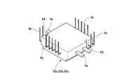
- An enlarged perspective view of a block module of a semiconductor device according to a seventh embodiment of the present invention Schematic diagram showing the cross-sectional structure of a semiconductor device in the prior art
- the semiconductor device and the method of manufacturing the same according to the present invention will be described below based on each embodiment.
- the semiconductor device of the present invention is, for example, a power device or a power module.
- this invention is not limited to IGBT, It is applicable also to the semiconductor device using another power transistor.
- Embodiment 1 The semiconductor device and the method of manufacturing the same according to the first embodiment of the present invention will be described with reference to FIGS. Note that, in FIGS. 1 to 10, the X direction and the Y direction are illustrated as appropriate in order to clarify the correspondence between the respective drawings.
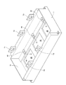
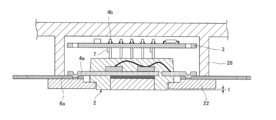
- FIG. 1 is a cross-sectional view showing the configuration of a semiconductor device 100 manufactured using the manufacturing method of the first embodiment.
- a semiconductor device 100 is configured by assembling an exterior case 1, a block module 2, and a control board 3.
- the exterior case 1 is an example of an exterior body, and is made of resin.
- a thermosetting epoxy resin for transfer molding can be used as the resin constituting the exterior case 1.
- An opening 20 is formed in the recess 19 of the outer case 1.
- a thin portion 48 is formed around the opening 20.
- the exterior case 1 has an external connection terminal 6 a whose one end is exposed at the bottom of the recess 19.
- the external connection terminal 6 a is insert-molded in the outer case 1.
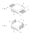
- the block module 2 incorporates the power semiconductor element 11 a, the lead frame 4, the aluminum wire 14, the insulating layer 16, and the heat sink 17. From the block module 2, a first lead 4a and a second lead 4b are drawn out.
- the first lead 4a is a power system input / output lead.
- the second lead 4b is a control signal input lead.
- the second lead 4b is drawn vertically bent upward from the block module 2 as shown in FIG. 6 (b).
- the first lead 4 a is horizontally drawn from the block module 2.
- the first lead 4 a and the second lead 4 b are part of the lead frame 4.
- the control element 8 and the passive component 9 are mounted on the control board 3 to construct an electric circuit for control signal generation.
- the passive component 9 is, for example, a resistor or a capacitor. Further, as shown in FIG. 7, through holes 18 and through holes 38 are formed in the control substrate 3.
- the second lead 4 b is electrically joined to the control substrate 3 by soldering or the like in a state of being inserted into the through hole 18 of the control substrate 3.
- the shape of the second lead 4 b is a shape bent in a direction away from the block module 2.
- a protrusion 7 is formed in the middle of the second lead 4b. The projection 7 engages with the back surface of the control board 3 to restrict the positional relationship between the block module 2 and the control board 3, and forms a predetermined interval between the block module 2 and the control board 3.
- the first lead 4a is electrically joined to the external connection terminal 6a by being crimped in a state of being superimposed on the exposed surface of the external connection terminal 6a.
- the bottom surface 2 aa of the block module 2 in a state in which the first lead 4 a and the external connection terminal 6 a are electrically connected slightly protrudes to the outside of the bottom surface 1 a of the exterior case 1.
- the recess 19 is not filled with the silicone gel 113 or the like shown in FIG. Therefore, an air layer 21 is formed between the control module 3 and the block module 2 whose distance is maintained by the projections 7.
- a lid 32 shown by an imaginary line may be attached to the upper opening of the recess 19.
- a control signal is supplied from the control substrate 3 to the gate terminal of the power semiconductor element 11a of the block module 2 via the second lead 4b, whereby the source terminal of the power semiconductor element 11a It controls on-off between drain terminals.
- the semiconductor device 100 according to the first embodiment can be manufactured in the first to seventh steps shown in FIGS. 5 (a) to 5 (g).
- the manufacturing process of the semiconductor device 100 of the first embodiment will be described with reference to FIGS. 5 (a) to 5 (g).
- the insulating layer 16 and the heat sink 17 are bonded to the back surface of the lead frame 4. That is, the heat sink 17 is thermally connected to the power semiconductor element 11 a via the lead frame 4 and the insulating layer 16.
- the insulating layer 16 is a layer having adhesiveness.
- the insulating layer 16 and the heat sink 17 are previously bonded and processed into a desired shape, and then they are bonded to the lead frame 4.
- the adherend of the insulating layer 16 is the heat radiation plate 17 and the lead frame 4, so when the resin is bonded in advance, the resin is completely cured to lose adhesion.
- FIG. 6 (a) shows the block module 2 in the state of FIG. 5 (c). As shown in FIG. 6A, one end of the second lead 4 b is connected to the control signal input circuit of the block module 2 and is pulled out of the block module 2.
- a forming process is performed to bend the second lead 4 b upward by 90 ° so as to be separated from the block module 2.
- the state shown in FIG. 6B is obtained.
- a mounting structure 36 in which three block modules 2 are mounted on the control substrate 3 is created.
- the second leads 4b of each block module 2 are inserted into the through holes 18 of the control board 3, and the second leads 4b and the control board 3 are electrically connected by means such as soldering. Bond to and secure. Since the projections 7 are formed on the second leads 4b, the control substrate 3 is supported by the projections 7, and the distance between the block module 2 and the control substrate 3 can be set to a predetermined distance. In addition, if the tip of the second lead 4 b is tapered, it can be easily inserted into the through hole 18.
- the mounting structure 36 created in this manner is shown in FIG.
- the mounting structure 36 is inserted into the recess 19 of the outer case 1.
- the position of the mounting structure 36 inserted in the recess 19 in the Y direction is positioned such that the tip of the thin portion 48 abuts the groove 37 of the block module 2 .
- the position in the Y direction of the mounting structure 36 inserted in the concave portion 19 is engaged with the groove 37 formed in the bottom of the block module 2 with the thin portion 48 around the opening 20 of the exterior case 1 Is positioned.
- the groove 37 at the bottom of the block module 2 can also be formed by the above-described sealing mold, and can also be formed by cutting after sealing.
- FIG. 8 A bottom view of the semiconductor device 100 is shown in FIG. Further, in the state of FIG. 5 (f), as shown in FIG. 8, the first leads 4 a of each block module 2 (2 a, 2 b, 2 c) are terminals T 1, T 2, T 3 provided on the exterior case 1. It overlaps with the external connection terminal 6a (positive electrode terminal P, negative electrode terminal N, load connection terminal C).
- the width d of the first lead 4a and the width D of the external connection terminal 6a of the exterior case 1 are both 1 mm to 10 mm and “d ⁇ D” when the semiconductor device 100 has the 75 A (ampere) specification. Is preferred.
- a plurality of control boards 3 are provided corresponding to the overlapping positions of the first leads 4a of the block modules 2 and the external connection terminals 6a.
- the through holes 38 are formed in advance.
- the first lead 4 a and the external connection terminal 6 a are joined (for example, , Can be crimped).
- the overlapping position of the first lead 4a and the external connection terminal 6a is a position at which the first lead 4a and the external connection terminal 6a overlap in the XY plane.
- a caulking tool 39 as an example of a bonding tool is inserted from the through hole 38 of the control substrate 3 toward the first lead 4a, The lead 4a is joined to the external connection terminal 6a.
- the first leads 4a of the block module 2 and the external connection terminals 6a of the exterior case 1 are electrically connected by caulking with a caulking tool 39 and joining them.
- the recess 40 is formed in the external connection terminal 6a, a part of the first lead 4a is pushed into the recess 40 of the external connection terminal 6a by caulking with the caulking tool 39. ing. Therefore, in the first embodiment, the first lead 4a and the external connection terminal 6a are firmly joined.
- the semiconductor device 100 shown in FIG. 1 can be manufactured by the assembling steps of the first to seventh steps described above.
- the second leads 4b of each block module 2 are inserted into the through holes 18 of the control board 3, and the second leads 4b and the control board 3 are electrically joined by means such as soldering.
- the fixing operation can be performed outside the exterior case 1. Therefore, the method of manufacturing the semiconductor device 100 according to the first embodiment is easy in work and good in workability.
- the semiconductor device 100 according to the first embodiment can be energized and inspected in the state of the mounting structure 36 in the process of manufacturing, it is possible to further improve the yield.
- the mounting structure 36 may be prepared regardless of the shape of the terminals T1 to T5 protruding to the outside of the exterior case 1 it can. Therefore, a plurality of types of mounting structures 36 can be prepared in advance and assembled to the exterior case 1 like a unit structure. Specifically, as soon as the shapes of the terminals T1 to T5 of the outer case 1 are determined, the mounting structure 36 prepared in advance can be assembled to the outer case 1 in the process of FIG. 5 (f) (g). As described above, in the first embodiment, the productivity of the semiconductor device 100 can be improved by forming the mounting structure 36 in the process of manufacturing the semiconductor device 100.
- the heat dissipation plate 17 of the block module 2 can be reliably brought into contact with the casing or the heat dissipation plate of the target device, and the heat conductivity can be improved.
- the thermally conductive grease or the thermally conductive sheet is interposed between the casing of the target device or the heat sink and the heat sink 17, the thermal conductivity can be further improved.
- the through holes 38 formed in the control substrate 3 for inserting the crimping tool 39 are individually formed in the control substrate 3 corresponding to the crimping position.
- the same effect can be realized even if one through hole 41 is formed corresponding to a plurality of caulking positions close to each other.
- one through hole 41 instead of the plurality of through holes 38, although there is a possibility that the rigidity and elasticity of the control substrate 3 may be reduced, it is possible to reduce the time and effort when forming the through holes. .
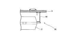
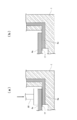
- FIG. 11 is a cross-sectional view of essential parts of a mounting structure used for a semiconductor device according to a second embodiment of the present invention.
- the second embodiment is the same as the first embodiment except that the mounting structure 36 of the above-described first embodiment is replaced with the mounting structure 56, and therefore, the description other than the mounting structure 56 is omitted.
- the mounting structure 36 in the first embodiment described above is configured by mounting the control board 3 on the tip of the second lead 4 b which is drawn out from the block module 2 and further bent.
- the mounting structure 56 of the second embodiment includes the block module 2 via the intermediate member 44 in the J lead (J-leads) shape electrically connected to the second lead 4 b. And the control board 3 are electrically connected.
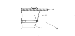
- FIG. 12 is a cross-sectional view of essential parts of a mounting structure used for a semiconductor device according to a third embodiment of the present invention.
- the third embodiment is the same as the first embodiment except that the mounting structure 36 of the above-described first embodiment is replaced with the mounting structure 66, and therefore the description other than the mounting structure 66 is omitted.
- intermediate member 44 can absorb the variation and block module 2. It is possible to regulate the relative position of the control board 3 and the control board 3.
- Embodiment 4 A semiconductor device according to a fourth embodiment of the present invention and a method of manufacturing the same will be described with reference to FIGS. 13, 14 and 15.
- FIG. 13 is a cross-sectional view showing a semiconductor device manufactured using the manufacturing method of the fourth embodiment.
- the recess 19 is formed and the external connection terminal 6a is insert-molded.
- the external case 51 is attached to the plate-like base portion 22 having the external connection terminal 6a and the plate-like base portion 22 for control.
- a guard portion 23 surrounding the periphery of the substrate 3 and the like is formed. That is, the exterior case 51 of the fourth embodiment is configured by combining two members (the base portion 22 and the guard portion 23).
- the configuration of the block module 2 and the control board 3 and the assembly of the block module 2 and the control board 3 are the same as in the first embodiment, and thus the description thereof is omitted.
- the semiconductor device of the fourth embodiment is assembled in the eighth to tenth steps described below.
- the mounting structure 36 is installed in the opening 50 of the base 22 before the guard 23 is attached. At this time, the first lead 4 a of the mounting structure 36 is disposed so as to overlap the external connection terminal 6 a of the base portion 22.
- the crimping tool 39 is inserted from the through hole 38, and the first lead 4a and the external connection terminal 6a are crimped. By this caulking process, the first lead 4a and the external connection terminal 6a are electrically joined. At this time, the caulking tool 39 is inserted into the through hole 38 as shown by a phantom line in FIG.
- the guard portion 23 is attached to the base portion 22 so as to surround the mounting structure 36.
- the cover 26 covering the periphery of the control board 3 can be formed by a part of the installation target device, the cover 26 should be disposed as shown in FIG. 15 instead of FIG. Thus, the guard 23 can be eliminated.
- the mounting structure 36 including the control substrate 3 having a size substantially equal to the inner dimension of the outer case 1 is housed in the recess 19 of the outer case 1.
- the dimension required for inserting the caulking tool 39 between the recess 19 of the outer case 1 A control substrate 73 capable of providing the gap 46 is used. In this case, the control board 73 does not need the through hole 38 in the first embodiment described above.
- the crimping tool 39 can be inserted from the gap 46 and caulking can be performed. Then, by this crimping process, it is possible to obtain a semiconductor device having the same function as that of the first embodiment described above.
- the first lead 4a and the external connection terminal 6a are electrically connected by caulking.
- other methods can be selected as long as the first lead 4a and the external connection terminal 6a are electrically connected through the through hole 38 or the like.
- Other methods include, for example, laser bonding by a laser passing through the through hole 38, ultrasonic bonding by a tool through the through hole 38, thermal bonding by a tool through the through hole 38, and chemical reaction. Chemical bonding by activating the bonding surface.
- Example 1 shown in FIG. 17 is an example in which the external connection terminal 6a and the first lead 4a are joined by ultrasonic bonding.
- the material of the external connection terminal 6a and the material of the first lead 4a are the same.
- the materials of the external connection terminal 6a and the first lead 4a are both copper.
- the first ultrasonic head 78 As shown in FIG. 17A, even if the oxide film 77 is formed on the surface of the external connection terminal 6a or the first lead 4a, the first ultrasonic head 78 as a bonding tool By pressing the lead 4a against the external connection terminal 6a and applying ultrasonic vibration in the direction of the arrow 79 to the contact surface of the first lead 4a and the external connection terminal 6a, as shown in FIG.
- the oxide film 77 interposed on the contact surface can be removed.
- the clean surfaces of the first lead 4a and the external connection terminal 6a are pressure-welded, and the first lead 4a and the external connection terminal 6a can be joined.
Landscapes
- Inverter Devices (AREA)
- Chemical & Material Sciences (AREA)
- Engineering & Computer Science (AREA)
- Materials Engineering (AREA)
- Structures Or Materials For Encapsulating Or Coating Semiconductor Devices Or Solid State Devices (AREA)
- Cooling Or The Like Of Semiconductors Or Solid State Devices (AREA)
Abstract
Description
図1~図10を用いて、本発明の実施の形態1の半導体装置及びその製造方法を説明する。なお、図1~図10では、それぞれの図の対応関係を明確にするために、適宜、X方向、Y方向を図示している。
図11は、本発明の実施の形態2の半導体装置に使用する実装構造体の要部断面図である。本実施の形態2は、前述の実施の形態1の実装構造体36を実装構造体56に置き換えた以外は実施の形態1と同様であるため、実装構造体56以外の説明は省略する。
図12は、本発明の実施の形態3の半導体装置に使用する実装構造体の要部断面図である。本実施の形態3は、前述の実施の形態1の実装構造体36を実装構造体66に置き換えた以外は実施の形態1と同様であるため、実装構造体66以外の説明は省略する。
図13,図14,図15を用いて、本発明の実施の形態4の半導体装置およびその製造方法を説明する。
図16を用いて、本発明の実施の形態5の半導体装置の製造方法を説明する。
上記の各実施の形態では、第1リード4aと外部接続端子6aとをカシメ処理によって電気接合したが、貫通孔38などを通して電気接合可能であれば、他の工法を選択することもできる。他の工法としては、例えば、貫通孔38を通過したレーザによるレーザ接合方法や、貫通孔38を通した工具による超音波接合方法、貫通孔38を通した工具による加熱接合、化学反応を利用して接合面を活性化することによる化学接合などがある。
図17に示す実施例1は、超音波接合によって、外部接続端子6aと第1リード4aとを接合している例である。この実施例では、外部接続端子6aの材質と第1リード4aの材質が同一である。具体的には、外部接続端子6aと第1リード4aの材質が、共に銅である。
図18に示す実施例2は、加熱接合によって、外部接続端子6aと第1リード4aとを接合している例である。図18は、加熱すると共に加圧することによって、外部接続端子6aと第1リード4aとを接合している。この実施例2では、外部接続端子6aの材質と第1リード4aの材質が同一である。具体的には、外部接続端子6aと第1リード4aの材質が、共に銅である。
図19に示す実施例3は、化学接合によって、外部接続端子6aと第1リード4aとを接合している例である。図19は、化学反応を利用して接合面を活性化することによって、外部接続端子6aと第1リード4aとを接合している。この実施例では、外部接続端子6aの材質と第1リード4aの材質が同一である。具体的には、外部接続端子6aと第1リード4aの材質が、共に銅である。
上記の各実施の形態において、第1リード4aと第2リード4bは、図6(b)に示したように、樹脂モールドされているブロックモジュール2a,2b,2cの別々の辺から引き出されていたが、本実施の形態では、図20,図21に示すように、ブロックモジュール92a,92b,92cは、第1リード4aが引き出されている辺と同じ辺から第2リード4bが引き出されている。
1a,2aa 底面
2,2a,2b,2c,92a,92b,92c ブロックモジュール
3,73 制御基板
4 リードフレーム
4a パワー系入出力リード
4b 制御信号入力リード
6a 外部接続端子
7 突起
8 制御素子
9 受動部品
11a パワー半導体素子
11b ダイオード
14 アルミ線
15 樹脂
16 絶縁層
17 放熱板
18 スルーホール
19,40,59,83,84 凹部
20,50 開口
21 空気層
22 ベース部
23 ガード部
26 カバー
32 蓋
33 負荷
34 取り付け孔
35 リング
36,56,66,76 実装構造体
37 溝
38,41 貫通孔
39 カシメツール
42,43 切り欠き
44,45 中間部材
48 薄肉部
P 正極端子
N 負極端子
C 負荷接続端子
T1~T5 端子
100 半導体装置
Claims (20)
- パワー半導体素子を内蔵し、第1リード及び第2リードが引き出されたブロックモジュールと、
前記パワー半導体素子を制御する制御基板と、
載置された前記ブロックモジュールの前記第1リードに当接する外部接続端子を有する外装体と、を備え、
前記第2リードは、前記制御基板に接続され、
前記第1リードは、前記外部接続端子に接合されている、
半導体装置。 - 前記第1リードと前記外部接続端子との重なり位置に対応する前記制御基板の領域に、貫通孔が形成された、
請求項1に記載の半導体装置。 - 前記第1リードと前記外部接続端子との重なり位置に対応する前記制御基板の領域に、切り欠きが形成された、
請求項1に記載の半導体装置。 - 前記第1リードと前記外部接続端子との重なり位置において、前記制御基板と前記第1リードとが重ならない、
請求項1に記載の半導体装置。 - 前記ブロックモジュールには、前記パワー半導体素子と熱接続する放熱板が、その一部を露出させた状態でモールドされており、
前記外装体には、前記ブロックモジュールの表面に露出した前記放熱板を露出させる開口が底部に形成されている、
請求項1~請求項4の何れか1項に記載の半導体装置。 - 前記ブロックモジュールには溝が形成されており、前記溝が前記開口周囲の前記外装体の薄肉部に係合している、
請求項5に記載の半導体装置。 - 前記第1リードと前記外部接続端子とがカシメ接合されている、
請求項1~請求項6の何れか1項に記載の半導体装置。 - 前記第2リードは、前記ブロックモジュールから離れる方向に曲げられた形状を有する、
請求項1~請求項7の何れか1項に記載の半導体装置。 - 前記第2リードに設けられた突起により、前記ブロックモジュールと前記制御基板の位置関係が規制されている、
請求項1~請求項8の何れか1項に記載の半導体装置。 - 前記ブロックモジュールと前記制御基板との間に空気層が形成されている、
請求項1~請求項9の何れか1項に記載の半導体装置。 - 前記第2リードと前記制御基板とが、中間部材を介して接続されている、
請求項1~請求項10の何れか1項に記載の半導体装置。 - 前記中間部材が、Jリード形状である、
請求項11に記載の半導体装置。 - 前記中間部材が、ガルウィング形状である、
請求項11に記載の半導体装置。 - 請求項1~請求項13の何れか1項に記載の半導体装置を組み込んだ装置。
- パワー半導体素子を内蔵し、第1リードと第2リードとが引き出されたブロックモジュールを準備し、
前記ブロックモジュールを前記制御基板に取り付けると共に、前記第2リードを前記制御基板に接続して実装構造体を形成し、
前記第1リードと外装体の外部接続端子とが重なるように前記実装構造体と前記外装体とを位置合わせした状態で、前記第1リードと前記外部接続端子との当接面を接合する、
半導体装置の製造方法。 - 前記第1リードと前記外部接続端子との当接面をカシメ接合する、
請求項15に記載の半導体装置の製造方法。 - 前記第1リードと前記外部接続端子との重なり位置に対応して前記制御基板に形成されている貫通孔又は切り欠きから、接合ツールを挿入して前記第1リードと前記外部接続端子の当接面を接合する、
請求項15又は請求項16に記載の半導体装置の製造方法。 - 前記実装構造体を形成するに際し、前記第2リードに設けられた突起により、前記ブロックモジュールと前記制御基板の位置関係を規制する、
請求項15~請求項17の何れか1項に記載の半導体装置の製造方法。 - 前記実装構造体と前記外装体との位置合わせを、前記ブロックモジュールに形成された溝を前記外装体に係合して行う、
請求項15~請求項18の何れか1項に記載の半導体装置の製造方法。 - 前記実装構造体と前記外装体とを位置合わせするに際し、前記ブロックモジュールの放熱板を前記外装体の開口から突出させる、
請求項15~請求項19の何れか1項に記載の半導体装置の製造方法。
Priority Applications (4)
| Application Number | Priority Date | Filing Date | Title |
|---|---|---|---|
| JP2013526015A JP5661183B2 (ja) | 2012-02-13 | 2012-12-10 | 半導体装置およびその製造方法 |
| CN201280011342.2A CN103430307B (zh) | 2012-02-13 | 2012-12-10 | 半导体装置及其制造方法 |
| EP12866999.1A EP2816598B1 (en) | 2012-02-13 | 2012-12-10 | Semiconductor device and method for manufacturing same |
| US13/982,720 US9136193B2 (en) | 2012-02-13 | 2012-12-10 | Semiconductor device and method of manufacturing the same |
Applications Claiming Priority (2)
| Application Number | Priority Date | Filing Date | Title |
|---|---|---|---|
| JP2012-027895 | 2012-02-13 | ||
| JP2012027895 | 2012-02-13 |
Publications (1)
| Publication Number | Publication Date |
|---|---|
| WO2013121491A1 true WO2013121491A1 (ja) | 2013-08-22 |
Family
ID=48983661
Family Applications (1)
| Application Number | Title | Priority Date | Filing Date |
|---|---|---|---|
| PCT/JP2012/007864 Ceased WO2013121491A1 (ja) | 2012-02-13 | 2012-12-10 | 半導体装置およびその製造方法 |
Country Status (5)
| Country | Link |
|---|---|
| US (1) | US9136193B2 (ja) |
| EP (1) | EP2816598B1 (ja) |
| JP (1) | JP5661183B2 (ja) |
| CN (1) | CN103430307B (ja) |
| WO (1) | WO2013121491A1 (ja) |
Cited By (8)
| Publication number | Priority date | Publication date | Assignee | Title |
|---|---|---|---|---|
| JP2017135873A (ja) * | 2016-01-28 | 2017-08-03 | 三菱電機株式会社 | パワーモジュール |
| JP2018195714A (ja) * | 2017-05-17 | 2018-12-06 | 富士電機株式会社 | パワー半導体モジュールおよびパワー半導体装置 |
| WO2019011890A1 (en) | 2017-07-12 | 2019-01-17 | Abb Schweiz Ag | POWER SEMICONDUCTOR MODULE |
| JP2022037739A (ja) * | 2020-08-25 | 2022-03-09 | 富士電機株式会社 | 半導体装置及び半導体装置の製造方法 |
| CN115398619A (zh) * | 2020-04-17 | 2022-11-25 | 西门子股份公司 | 具有壳体的半导体模块 |
| WO2024009753A1 (ja) * | 2022-07-05 | 2024-01-11 | ローム株式会社 | 半導体装置および半導体装置ユニット |
| KR102645308B1 (ko) * | 2022-09-14 | 2024-03-08 | 주식회사 아모센스 | 파워 모듈 |
| JP2024121220A (ja) * | 2023-02-27 | 2024-09-06 | 三菱電機株式会社 | 半導体装置および電力変換装置 |
Families Citing this family (38)
| Publication number | Priority date | Publication date | Assignee | Title |
|---|---|---|---|---|
| WO2014147787A1 (ja) * | 2013-03-21 | 2014-09-25 | 三菱電機株式会社 | 半導体装置 |
| DE102013104949B3 (de) * | 2013-05-14 | 2014-04-24 | Semikron Elektronik Gmbh & Co. Kg | Leistungselektronische Schalteinrichtung und Anordnung hiermit |
| JP2015026820A (ja) * | 2013-06-18 | 2015-02-05 | 株式会社デンソー | 電子装置 |
| JP6299120B2 (ja) * | 2013-09-05 | 2018-03-28 | 富士電機株式会社 | 半導体モジュール |
| JP6154342B2 (ja) * | 2013-12-06 | 2017-06-28 | トヨタ自動車株式会社 | 半導体装置 |
| JP2015220429A (ja) * | 2014-05-21 | 2015-12-07 | ローム株式会社 | 半導体装置 |
| JP6451257B2 (ja) * | 2014-11-21 | 2019-01-16 | 富士電機株式会社 | 半導体装置 |
| CN105990265B (zh) * | 2015-02-26 | 2019-04-05 | 台达电子工业股份有限公司 | 功率转换电路的封装模块及其制造方法 |
| CN105990266B (zh) * | 2015-02-26 | 2018-12-07 | 台达电子工业股份有限公司 | 功率转换电路的封装模块及其制造方法 |
| JP6515694B2 (ja) * | 2015-06-12 | 2019-05-22 | 富士電機株式会社 | 半導体装置 |
| US9743531B2 (en) * | 2015-06-29 | 2017-08-22 | Denso Corporation | Electronic apparatus and manufacturing method of electronic apparatus |
| WO2017130381A1 (ja) * | 2016-01-29 | 2017-08-03 | 三菱電機株式会社 | 半導体装置 |
| DE112017001646T5 (de) * | 2016-03-30 | 2019-01-03 | Mitsubishi Electric Corporation | Leistungsmodul und verfahren zum herstellen desselben, sowie leistungselektronik-vorrichtung und verfahren zum herstellen derselben |
| JP6920790B2 (ja) * | 2016-05-24 | 2021-08-18 | ローム株式会社 | インテリジェントパワーモジュール、電気自動車またはハイブリッドカー、およびインテリジェントパワーモジュールの組み立て方法 |
| JP6490027B2 (ja) * | 2016-06-10 | 2019-03-27 | 三菱電機株式会社 | 半導体装置 |
| JP6546892B2 (ja) * | 2016-09-26 | 2019-07-17 | 株式会社 日立パワーデバイス | 半導体装置 |
| JP6755197B2 (ja) * | 2017-01-19 | 2020-09-16 | 三菱電機株式会社 | 半導体装置およびその製造方法 |
| JP6859860B2 (ja) * | 2017-06-13 | 2021-04-14 | 株式会社デンソー | 電力変換装置、及びその製造方法 |
| DE112018003850B4 (de) | 2017-07-28 | 2023-04-27 | Mitsubishi Electric Corporation | Halbleitereinheit und halbleitermodul |
| KR102445515B1 (ko) * | 2017-09-29 | 2022-09-21 | 현대자동차주식회사 | 차량용 전력모듈 |
| JP6988345B2 (ja) * | 2017-10-02 | 2022-01-05 | 株式会社デンソー | 半導体装置 |
| JP2019087636A (ja) * | 2017-11-07 | 2019-06-06 | 富士電機株式会社 | 半導体パッケージ |
| US10667439B1 (en) | 2018-11-01 | 2020-05-26 | Franklin Electric Company, Inc. | Discrete power component assembly |
| FR3089749B1 (fr) * | 2018-12-05 | 2020-11-27 | Valeo Equip Electr Moteur | Module électronique |
| CN109801900B (zh) * | 2019-01-15 | 2021-10-29 | 江苏双聚智能装备制造有限公司 | 一种电力用逆变电路装置 |
| JP7190985B2 (ja) * | 2019-08-05 | 2022-12-16 | 三菱電機株式会社 | 半導体装置 |
| DE112019007624T5 (de) * | 2019-08-09 | 2022-04-21 | Mitsubishi Electric Corporation | Halbleitervorrichtung |
| US11387179B2 (en) * | 2019-12-10 | 2022-07-12 | Texas Instruments Incorporated | IC package with half-bridge power module |
| JP7313302B2 (ja) * | 2020-03-18 | 2023-07-24 | 三菱電機株式会社 | 半導体装置および半導体装置の製造方法 |
| KR102819516B1 (ko) * | 2020-04-20 | 2025-06-11 | 현대자동차주식회사 | 솔더링 구조, 이를 갖는 파워 모듈 및 파워 모듈의 제조 방법 |
| CN111863763A (zh) * | 2020-06-30 | 2020-10-30 | 扬州国扬电子有限公司 | 一种结构紧凑型ipm功率模块 |
| CN115777145B (zh) * | 2020-07-14 | 2024-10-22 | 三菱电机株式会社 | 半导体装置以及电力变换装置 |
| EP4203010B1 (en) * | 2020-09-15 | 2025-07-30 | Huawei Technologies Co., Ltd. | Power module, converter, and electronic device |
| DE112020007719T5 (de) * | 2020-10-20 | 2023-08-10 | Mitsubishi Electric Corporation | Halbleitervorrichtung |
| US20220396154A1 (en) * | 2021-06-14 | 2022-12-15 | Panasonic Intellectual Property Management Co., Ltd. | Vehicle mounted electric power converter |
| US12113000B2 (en) * | 2021-12-02 | 2024-10-08 | Infineon Technologies Ag | Lead adapters for semiconductor package |
| TWI876247B (zh) * | 2022-12-21 | 2025-03-11 | 能創半導體股份有限公司 | 功率模組 |
| CN116364671A (zh) * | 2023-03-09 | 2023-06-30 | 华为数字能源技术有限公司 | 一种功率变换器、封装结构以及散热结构 |
Citations (5)
| Publication number | Priority date | Publication date | Assignee | Title |
|---|---|---|---|---|
| JP2001189416A (ja) * | 1999-12-28 | 2001-07-10 | Mitsubishi Electric Corp | パワーモジュール |
| JP2003100987A (ja) * | 2001-09-20 | 2003-04-04 | Mitsubishi Electric Corp | 半導体装置 |
| JP2003243609A (ja) | 2002-02-18 | 2003-08-29 | Mitsubishi Electric Corp | 電力半導体装置及びその製造方法 |
| JP4108909B2 (ja) | 2000-08-25 | 2008-06-25 | 三菱電機株式会社 | 半導体装置 |
| JP2010283014A (ja) * | 2009-06-02 | 2010-12-16 | Mitsubishi Electric Corp | 電力変換装置及びその製造方法 |
Family Cites Families (10)
| Publication number | Priority date | Publication date | Assignee | Title |
|---|---|---|---|---|
| JP3130239B2 (ja) | 1995-08-02 | 2001-01-31 | 松下電子工業株式会社 | 樹脂封止型半導体装置およびその製造方法 |
| JP4218193B2 (ja) * | 2000-08-24 | 2009-02-04 | 三菱電機株式会社 | パワーモジュール |
| JP2006303006A (ja) * | 2005-04-18 | 2006-11-02 | Yaskawa Electric Corp | パワーモジュール |
| DE102005050534B4 (de) | 2005-10-21 | 2008-08-07 | Semikron Elektronik Gmbh & Co. Kg | Leistungshalbleitermodul |
| JP4760585B2 (ja) * | 2006-07-18 | 2011-08-31 | 三菱電機株式会社 | 電力用半導体装置 |
| JP4695041B2 (ja) | 2006-08-09 | 2011-06-08 | 本田技研工業株式会社 | 半導体装置 |
| US7701054B2 (en) | 2007-02-12 | 2010-04-20 | Infineon Technologies Ag | Power semiconductor module and method for its manufacture |
| JP4969388B2 (ja) * | 2007-09-27 | 2012-07-04 | オンセミコンダクター・トレーディング・リミテッド | 回路モジュール |
| JP4634498B2 (ja) | 2008-11-28 | 2011-02-16 | 三菱電機株式会社 | 電力用半導体モジュール |
| JP2011086889A (ja) * | 2009-10-19 | 2011-04-28 | Renesas Electronics Corp | 半導体装置およびその製造方法 |
-
2012
- 2012-12-10 WO PCT/JP2012/007864 patent/WO2013121491A1/ja not_active Ceased
- 2012-12-10 US US13/982,720 patent/US9136193B2/en active Active
- 2012-12-10 EP EP12866999.1A patent/EP2816598B1/en active Active
- 2012-12-10 JP JP2013526015A patent/JP5661183B2/ja active Active
- 2012-12-10 CN CN201280011342.2A patent/CN103430307B/zh active Active
Patent Citations (6)
| Publication number | Priority date | Publication date | Assignee | Title |
|---|---|---|---|---|
| JP2001189416A (ja) * | 1999-12-28 | 2001-07-10 | Mitsubishi Electric Corp | パワーモジュール |
| JP4108909B2 (ja) | 2000-08-25 | 2008-06-25 | 三菱電機株式会社 | 半導体装置 |
| JP2003100987A (ja) * | 2001-09-20 | 2003-04-04 | Mitsubishi Electric Corp | 半導体装置 |
| JP4177571B2 (ja) | 2001-09-20 | 2008-11-05 | 三菱電機株式会社 | 半導体装置 |
| JP2003243609A (ja) | 2002-02-18 | 2003-08-29 | Mitsubishi Electric Corp | 電力半導体装置及びその製造方法 |
| JP2010283014A (ja) * | 2009-06-02 | 2010-12-16 | Mitsubishi Electric Corp | 電力変換装置及びその製造方法 |
Non-Patent Citations (1)
| Title |
|---|
| See also references of EP2816598A4 |
Cited By (10)
| Publication number | Priority date | Publication date | Assignee | Title |
|---|---|---|---|---|
| JP2017135873A (ja) * | 2016-01-28 | 2017-08-03 | 三菱電機株式会社 | パワーモジュール |
| JP2018195714A (ja) * | 2017-05-17 | 2018-12-06 | 富士電機株式会社 | パワー半導体モジュールおよびパワー半導体装置 |
| WO2019011890A1 (en) | 2017-07-12 | 2019-01-17 | Abb Schweiz Ag | POWER SEMICONDUCTOR MODULE |
| US11362008B2 (en) | 2017-07-12 | 2022-06-14 | Hitachi Energy Switzerland Ag | Power semiconductor module embedded in a mold compounded with an opening |
| CN115398619A (zh) * | 2020-04-17 | 2022-11-25 | 西门子股份公司 | 具有壳体的半导体模块 |
| JP2022037739A (ja) * | 2020-08-25 | 2022-03-09 | 富士電機株式会社 | 半導体装置及び半導体装置の製造方法 |
| JP7528634B2 (ja) | 2020-08-25 | 2024-08-06 | 富士電機株式会社 | 半導体装置及び半導体装置の製造方法 |
| WO2024009753A1 (ja) * | 2022-07-05 | 2024-01-11 | ローム株式会社 | 半導体装置および半導体装置ユニット |
| KR102645308B1 (ko) * | 2022-09-14 | 2024-03-08 | 주식회사 아모센스 | 파워 모듈 |
| JP2024121220A (ja) * | 2023-02-27 | 2024-09-06 | 三菱電機株式会社 | 半導体装置および電力変換装置 |
Also Published As
| Publication number | Publication date |
|---|---|
| CN103430307A (zh) | 2013-12-04 |
| CN103430307B (zh) | 2016-04-27 |
| EP2816598B1 (en) | 2020-03-18 |
| JP5661183B2 (ja) | 2015-01-28 |
| JPWO2013121491A1 (ja) | 2015-05-11 |
| EP2816598A4 (en) | 2015-06-24 |
| US20140299982A1 (en) | 2014-10-09 |
| US9136193B2 (en) | 2015-09-15 |
| EP2816598A1 (en) | 2014-12-24 |
Similar Documents
| Publication | Publication Date | Title |
|---|---|---|
| JP5661183B2 (ja) | 半導体装置およびその製造方法 | |
| JP5696780B2 (ja) | 半導体装置およびその製造方法 | |
| CN104285294B (zh) | 半导体装置及该半导体装置的制造方法 | |
| CN103493197B (zh) | 半导体装置及其制造方法 | |
| CN101626001B (zh) | 半导体装置及其制造方法 | |
| US9202765B2 (en) | Semiconductor device | |
| US9935074B2 (en) | Semiconductor device and method for manufacturing same | |
| JP2017163135A (ja) | 半導体モジュール | |
| JP5895220B2 (ja) | 半導体装置の製造方法 | |
| US11315850B2 (en) | Semiconductor device | |
| JP2012182250A (ja) | 半導体装置 | |
| JP2020072094A (ja) | パワーユニット、パワーユニットの製造方法及びパワーユニットを有する電気装置 | |
| JP2013033874A (ja) | パワーモジュール | |
| CN118824964B (zh) | 一种智能功率模块、控制器以及家用电器 | |
| US20240071876A1 (en) | Semiconductor module, power converter, and power converter manufacturing method | |
| WO2022202638A1 (ja) | 回路装置 | |
| JP2024166626A (ja) | 半導体モジュール、および半導体モジュールの製造方法 | |
| JP2024126061A (ja) | 半導体モジュールの製造方法及び半導体モジュール | |
| JP2012253217A (ja) | 半導体モジュールおよびその製造方法 | |
| JP2007335728A (ja) | 絶縁型大電力用半導体装置 |
Legal Events
| Date | Code | Title | Description |
|---|---|---|---|
| WWE | Wipo information: entry into national phase |
Ref document number: 201280011342.2 Country of ref document: CN |
|
| ENP | Entry into the national phase |
Ref document number: 2013526015 Country of ref document: JP Kind code of ref document: A |
|
| WWE | Wipo information: entry into national phase |
Ref document number: 2012866999 Country of ref document: EP |
|
| 121 | Ep: the epo has been informed by wipo that ep was designated in this application |
Ref document number: 12866999 Country of ref document: EP Kind code of ref document: A1 |
|
| WWE | Wipo information: entry into national phase |
Ref document number: 13982720 Country of ref document: US |
|
| NENP | Non-entry into the national phase |
Ref country code: DE |