WO2013128767A1 - 撮像システム - Google Patents
撮像システム Download PDFInfo
- Publication number
- WO2013128767A1 WO2013128767A1 PCT/JP2012/083451 JP2012083451W WO2013128767A1 WO 2013128767 A1 WO2013128767 A1 WO 2013128767A1 JP 2012083451 W JP2012083451 W JP 2012083451W WO 2013128767 A1 WO2013128767 A1 WO 2013128767A1
- Authority
- WO
- WIPO (PCT)
- Prior art keywords
- control
- unit
- imaging
- control parameters
- communication unit
- Prior art date
- Legal status (The legal status is an assumption and is not a legal conclusion. Google has not performed a legal analysis and makes no representation as to the accuracy of the status listed.)
- Ceased
Links
Images



Classifications
-
- H—ELECTRICITY
- H04—ELECTRIC COMMUNICATION TECHNIQUE
- H04N—PICTORIAL COMMUNICATION, e.g. TELEVISION
- H04N7/00—Television systems
- H04N7/18—Closed-circuit television [CCTV] systems, i.e. systems in which the video signal is not broadcast
-
- A—HUMAN NECESSITIES
- A61—MEDICAL OR VETERINARY SCIENCE; HYGIENE
- A61B—DIAGNOSIS; SURGERY; IDENTIFICATION
- A61B1/00—Instruments for performing medical examinations of the interior of cavities or tubes of the body by visual or photographical inspection, e.g. endoscopes; Illuminating arrangements therefor
- A61B1/00002—Operational features of endoscopes
- A61B1/00004—Operational features of endoscopes characterised by electronic signal processing
- A61B1/00006—Operational features of endoscopes characterised by electronic signal processing of control signals
-
- A—HUMAN NECESSITIES
- A61—MEDICAL OR VETERINARY SCIENCE; HYGIENE
- A61B—DIAGNOSIS; SURGERY; IDENTIFICATION
- A61B1/00—Instruments for performing medical examinations of the interior of cavities or tubes of the body by visual or photographical inspection, e.g. endoscopes; Illuminating arrangements therefor
- A61B1/04—Instruments for performing medical examinations of the interior of cavities or tubes of the body by visual or photographical inspection, e.g. endoscopes; Illuminating arrangements therefor combined with photographic or television appliances
- A61B1/045—Control thereof
Definitions
- the present invention relates to an imaging system including an endoscope provided with an imaging device disposed at the distal end of the endoscope.
- the plurality of control parameters are sent from a control unit configured by, for example, an FPGA.
- a control unit configured by, for example, an FPGA.
- the control unit and the like are limited by a space restriction that can be secured around the imaging device.
- the connector connecting the endoscope and the processor the processor itself is provided.
- the cable connecting the image sensor disposed at the distal end of the endoscope insertion portion and the processor is a relatively long distance, and is close in the field of the procedure using the endoscope apparatus.
- noise sources such as electric scalpels, so noises due to disturbances are likely to be mixed into the connection cable, and there are concerns about problems such as disruption of signals transmitted and so-called communication data. Is done.
- An object of the present invention is to provide an imaging system capable of accurately transmitting a plurality of necessary control parameters and always performing normal imaging control.
- An imaging system includes an imaging device that generates and outputs an image signal by receiving light and performing photoelectric conversion, and a control device that transmits control parameters for driving and controlling the imaging device And an imaging system in which the imaging device and the control device can communicate with each other, the control system being provided in the control device, and having a plurality of control parameters for controlling imaging of the imaging device with respect to the imaging device.
- a first communication unit that transmits, a second communication unit that is provided in the imaging device and receives a control parameter transmitted from the first communication unit, and the plurality of received by the second communication unit
- a determination unit configured to determine whether or not the control parameter is normal; and the plurality of control parameters provided in the imaging apparatus and received by the second communication unit based on a determination result in the determination unit.
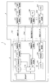
- FIG. 1 is a diagram illustrating an overall configuration of an imaging system according to a first embodiment of the present invention.
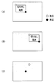
- FIG. 3 is a diagram for explaining an example of control parameters transmitted in the imaging system of the first embodiment.
- the figure which shows the structure of the electric system in the imaging system of the 4th Embodiment of this invention The figure which shows the structure of the electric system in the imaging system of the 6th Embodiment of this invention.
- the figure which shows the whole imaging system structure of the 8th Embodiment of this invention The figure which shows the whole structure of the imaging system of the 9th Embodiment of this invention.
- an imaging system 1 including an imaging device according to the first embodiment of the present invention includes an endoscope 2 including an imaging element 100 and an endoscope 2 that are detachably connected.
- a light source device 3 for supplying illumination light to the endoscope 2 and an endoscope 2 are detachably connected, and a processor 4 as a signal processing device for performing predetermined signal processing, and an image signal generated by the processor 4 as an endoscope
- a monitor 5 as a display device for displaying as an image.
- the endoscope 2 includes an elongated insertion portion 6 to be inserted into a body cavity, an operation portion 7 provided at the rear end of the insertion portion 6, and a universal cord 8 extending from the operation portion 7. .
- the universal cord 8 branches into a light guide cord 9 and a signal cord (signal cable) 10 near or in the middle of the base end.
- the light source connector 11 at the end of the light guide cord 9 is detachably connected to the light source device 3, and the signal connector 12 at the end of the signal cord 10 is detachably connected to the processor 4.
- a light guide 13 for transmitting illumination light is inserted through the insertion unit 6, the operation unit 7, and the universal cord 8. Then, by connecting the light source connector 11 to the light source device 3, the illumination light from the light source device 3 is transmitted by the light guide 13, and the light guide attached to the illumination window provided at the distal end portion 14 of the insertion portion 6. The transmitted illumination light is emitted from the tip surface.
- a connector in which the light source connector 11 and the signal connector 12 are integrated is connected to the light source device 3, and the signal of the signal connector 12 is exchanged with the processor 4 by a cable connecting the light source device 3 and the processor 4. You may make it the structure to do.
- the distal end portion 14 is provided with an observation window (imaging window) adjacent to the illumination window, and an objective lens 15 that connects an optical image of a subject such as an illuminated affected area is attached to the observation window.
- the CIS 100 is connected to a connector 16 provided inside the signal connector 12 via a total coaxial cable 101 inserted into the insertion portion 6 and the universal cord 8, and the connector 16 is detachable from the processor 4. Connected to.
- the processor 4 includes a power supply circuit (not shown) that generates a plurality of power supply voltages necessary for the operation of the image sensor and the like, and a signal processing circuit that performs predetermined signal processing on an image signal output from the image sensor (FIG. 1 is a diagram). And a control circuit (not shown in FIG. 1) for performing control including the power supply circuit and the signal processing circuit, and a plurality of control parameters for controlling the CIS 100 are provided to the CIS 100 For example, a control unit (FPGA) 200 configured by an FPGA and a memory 201 that stores information on the plurality of control parameters are provided.
- FPGA control unit
- Other components in the processor 4 will be described in detail later.
- control unit (FPGA) 200 reads various setting values relating to a plurality of control parameters from the memory 201 and transmits the setting values to the CIS 100 by communication via the integrated coaxial cable 101. .
- the transmission operation of the plurality of control parameters will be described in detail later.
- the control unit 200 is configured with an FPGA in the present embodiment, but is not limited thereto, and may be another communication device.
- the total coaxial cable 101 extends from the output end of the CIS 100 at the insertion portion 6 and is further detachably attached to the processor 4 via a connector 16 provided in the signal connector 12 through the universal cord 8. Connected to.
- the general coaxial cable 101 is a cable connecting the CIS 100 and the processor 4, and transmits a power supplied to the CIS 100 and also a video signal (serial signal) on which a synchronization signal transmitted from the CIS 100 is superimposed. ),
- the vertical synchronization signal (VD) transmitted from the processor 4, the communication contents of a plurality of control parameters transmitted from the processor 4 to the CIS 100, the error correction code or the error detection code, and the like are transmitted and received.
- the general coaxial cable 101 is shielded by a shield member by an exterior member of the insertion portion 6. Further, the shield member is electrically connected to a shield member by the exterior member of the operation unit 7, a shield member by the exterior member of the universal cord 8, a shield member of the signal connector 12, and the like.
- FIG. 2 is a block diagram showing the configuration of the electrical system in the imaging system of the present embodiment.
- An image sensor (CIS) 100 in the present embodiment is configured by a so-called CMOS (complementary metal oxide semiconductor) image sensor, and a light receiving element 111 disposed at an image forming position of the objective lens 15 and an output from the light receiving element 111.
- CMOS complementary metal oxide semiconductor
- AFE analog front end
- AFE 112 that removes noise from the received signal and digitizes it
- a synchronization superimposing circuit 113 that superimposes a synchronizing signal on the video signal that is the output signal of the AFE 112, and converts the video signal into a serial signal for transmission
- the P / S conversion circuit 114 for outputting to the outside, the video signal transmitting unit 115 for outputting the video signal (serial signal) to the outside, and the vertical synchronization signal (VD) from the external processor 4, for example.
- VD vertical synchronization signal
- Etc. and a synchronization signal receiving unit 116 that receives the synchronization signal receiving unit 116 received from the outside in a predetermined case.
- a predetermined process is performed on the signal (vertical synchronization signal (VD) received from the processor 4) and the synchronization signal processing unit 117 generates its own synchronization signal in the CIS 100, and the synchronization signal processing unit 117 performs the predetermined process.
- a timing generator (TG) 118 that causes the synchronization signal to follow the external synchronization signal subjected to the above and supplies it to each circuit as various synchronization signals in the CIS 100, and is transmitted from the control unit (FPGA) 200.
- Control parameter receiving unit 131 that receives the control parameter and the error correction code or error detection code, and the error correction code or error detection code added to the communication content of the control parameter received by the control parameter receiving unit 131 (this embodiment) The received control parameter based on the checksum code)
- a determination unit 132 whether or not a reception lay configured to include a, a register 133 for storing the control parameters and the like for use in imaging control in the CIS 100.
- the processor 4 receives a video signal (serial signal) having video data transmitted from the CIS 100 and a video signal on which a synchronization signal received by the video signal receiving unit 121 is superimposed.
- An S / P conversion circuit 122 that converts (serial signal) into a parallel signal; a signal processing unit 123 that performs predetermined signal processing on the received video signal and outputs the signal to the monitor 5; and image processing in the processor 4
- a timing generator (TG) 125 that generates a vertical synchronization signal (VD) for the circuit 4 and supplies it to various circuits, and a vertical synchronization signal (VD) in the processor 4 that is supplied from the timing generator (TG) 125 is supplied to the CIS 100.
- the synchronization signal transmitter 124 for transmitting to the A configured control unit (FPGA) 200 and a control parameter transmission unit 211 configured to transmit to the CIS 100 a plurality of control parameters configured in the control unit (FPGA) 200 for controlling the CIS 100.
- a memory 201 storing information relating to the plurality of control parameters.
- control parameter transmission unit 211 is configured in the control unit (FPGA) 200, but the other components, the timing generator (TG) 125, are configured in the FPGA. May be.
- control unit (FPGA) 200 reads various setting values related to a plurality of control parameters from the memory 201 at the time of activation, and the setting values are transmitted from the control parameter transmission unit 211 in the control unit (FPGA) 200.
- the data is transmitted to the CIS 100 via the integrated coaxial cable 101, for example, based on an I2C interface. Even after the activation, the corresponding control parameters are transmitted by communication in order to change the shooting mode, the gain setting, the electronic shutter setting, the cutout position setting and the like as necessary.
- the I2C interface is adopted as a communication method.
- the present invention is not limited to this, and other communication methods such as an SPI interface may be adopted.
- the control unit (FPGA) 200 reads various setting values related to a plurality of control parameters from the memory 201 and transmits the setting values to the CIS 100 via the total coaxial cable 101.
- the “plural control parameters” are classified into several groups. The plurality of control parameters belonging to each group is meaningful only when all the control parameters in the group are normally transmitted. In other words, in this embodiment, the plurality of control parameters belonging to a certain group. Are treated as a set of information grouped in advance.
- the plurality of control parameters transmitted in the imaging system of the present embodiment are classified into the following groups, for example.
- Group A is a plurality of control parameters related to brightness (dimming), and is specifically as follows.
- Gain CDS gain, digital gain, AGC
- Position of electronic shutter Binning setting (for example, setting for pixel addition, setting of how many pixels to add, its direction, etc.) If only a part of these control parameters are reflected, there is a risk that unintentional inappropriate brightness control may be performed. For example, since the brightness changes as the number of added pixels changes, it is desirable that the binning setting is controlled simultaneously with the gain setting and the electronic shutter setting.
- the group B is a control parameter group related to the address information of the correction position, and specifically corresponds to two parameters, parameters relating to x coordinate data and parameters relating to y coordinate data.
- the group B is a control parameter group related to the address information of the correction position, and specifically corresponds to two parameters, parameters relating to x coordinate data and parameters relating to y coordinate data.
- Group C> is a control parameter group that designates a predetermined “range” on the screen such as a cutout range. Specifically, there are various designation methods for designating the cutout range. For example, a parameter related to the start point position of cutout and a parameter related to the end point position are equivalent. The case where the parameter relating to the start point position and the parameter relating to the end point position are both transmitted correctly and not the layer will be described with reference to FIG.
- FIG. 3 is a diagram illustrating a transmission example of a parameter for designating a clipping range among a plurality of control parameters transmitted in the imaging system of the first embodiment.
- the cutout range As an initial state of the cutout range, for example, when the start point position and the end point position shown in FIG. 3A are specified, when the cutout range is changed to the position shown in FIG.
- the parameters related to the end point position are both transmitted accurately, they are reflected in the position shown in FIG. 3B.
- the parameter related to the start point position is accurately transmitted while the parameters related to the end point position are transmitted. If the parameter is not transmitted correctly, the relationship between the start point position and the end point position becomes abnormal as shown in FIG. 3C, and the cutout range does not exist.
- control parameter group In the present embodiment, the above three examples are given as the control parameter group. However, it is needless to say that the control parameter group is not limited to this. For other groups of information set in advance, Thus, the present invention may be applied.
- an error correction code such as a Hamming code
- an error detection code such as a parity bit and a checksum
- control unit (FPGA) 200 reads various setting values related to a plurality of control parameters from the memory 201, and the communication contents of the plurality of control parameters from the control parameter transmission unit 211. At the same time, an error correction code or error detection code (parity bit, checksum, etc.) is transmitted.
- FIG. 4 is a diagram illustrating an example in which a checksum code is added to the communication content of the control parameter related to brightness (dimming) transmitted in the imaging system of the first embodiment, and specifically, is transmitted.
- the checksum codes of all these functions are added to the gain setting, the electronic shutter setting, and the binning setting for transmission.
- the control parameter receiving unit 131 in the CIS 100 checks the communication contents related to the gain setting, electronic shutter setting, and binning setting transmitted from the control parameter transmitting unit 211 in the control unit (FPGA) 200, and all these functions. Sum code is received.
- the determination unit 132 determines whether or not the received control parameter is correctly transmitted and received based on the checksum code added to the communication content of the control parameter received by the control parameter reception unit 131.
- the result of determination by the determination unit 132 is that the checksum result is OK, the gain setting, electronic shutter setting, and binning setting are all reflected in the register 133.
- the determination unit 132 performs control so that all control parameters for gain setting, electronic shutter setting, and binning setting are not reflected in the register 133. . That is, when any setting value is already stored in the register 133, control is performed so that the newly received setting value is not updated.
- the checksum result when the checksum result is NG, all the settings related to the new control parameter are not reflected in the register 133, but instead of this, at the same time, the content that the checksum result is NG, that is, the content that the communication result is NG may be stored in another register (not shown) in the CIS 100.
- the content of the communication result being NG is sent to the control unit (FPGA) in the processor 4 via a signal line for transmitting a video signal from the CIS 100 or another signal line provided in advance between the CIS 100 and the processor 4. ) 200 may be notified.
- FPGA control unit
- a CMOS image sensor is disposed at the distal end of the endoscope insertion portion, and a plurality of preset control parameters necessary for imaging control from the processor side are obtained from the CMOS image.
- these multiple control parameters necessary for shooting control are treated as a set of information, and only when all the multiple control parameters are transmitted normally, information on these control parameters Is reflected in a register in the CMOS image senner, and if all of the plurality of control parameters are not normally transmitted, normal imaging control can be performed by controlling so as not to update the contents of the register.
- An imaging system can be provided.
- the imaging system of the second embodiment of the present invention has the same configuration as that of the first embodiment, but communication contents and error correction of a plurality of control parameters transmitted from the control parameter transmission unit 211 toward the CIS 100.
- the transmission contents of the code or error detection code are different. Since the other configuration is the same as that of the first embodiment, a detailed description thereof is omitted here.
- FIG. 5 is a diagram illustrating an example in which a checksum code is added to the communication content of a control parameter related to brightness (dimming) transmitted in the imaging system of the second embodiment, and specifically, is transmitted.
- a checksum code is added to each of gain setting, electronic shutter setting, and binning setting for transmission.
- control parameter receiving unit 131 in the CIS 100 is a communication content related to gain setting, electronic shutter setting, and binning setting transmitted from the control parameter transmitting unit 211 in the control unit (FPGA) 200. And a checksum code combined with each of them.
- the determination unit 132 determines whether each of the received plurality of control parameters has been correctly transmitted / received based on the checksum code associated with each control parameter added to the communication content of the control parameter received by the control parameter receiving unit 131. Determine whether or not.
- the determination unit 132 registers the register 133 for all control parameters of gain setting, electronic shutter setting, and binning setting. Control so that it is not reflected. In this case, if any setting value is already stored in the register 133, control is performed so that the newly received setting value is not updated, as in the first embodiment.
- the content that the checksum result is NG may be stored in another register (not shown) in the CIS 100, or The control unit (FPGA) in the processor 4 indicates that the communication result is NG via a signal line for transmitting a video signal from the CIS 100 or another signal line provided in advance between the CIS 100 and the processor 4. 200 may be notified.
- FPGA field-programmable gate array
- FIG. 5 shows an example in which a combination of the respective checksum codes is continuously transmitted for the gain setting, the electronic shutter setting, and the binning setting.
- the number of types is specified in the header in advance, and the control parameter receiving unit 131 or the determination unit 132 that is the receiver detects whether all types of control parameters have been transmitted, and a set of information groups It may be determined whether or not a plurality of control parameters are transmitted.
- a CMOS image sensor is disposed at the distal end of the endoscope insertion portion, and preset from the processor side necessary for shooting control.
- the plurality of control parameters necessary for imaging control are treated as a set of information groups, and all the plurality of control parameters are transmitted normally. Only when the control parameter information is reflected in the register in the CMOS image senor, and if any control parameter is not transmitted normally, control is performed so that the contents of the register are not updated for all control parameters. By doing so, it is possible to provide an imaging system that can always perform normal imaging control.
- the imaging system of the third embodiment of the present invention has the same configuration as that of the first and second embodiments, but communication contents of a plurality of control parameters transmitted from the control parameter transmission unit 211 toward the CIS 100.
- the transmission contents of the error correction code or error detection code are different from those of the first and second embodiments. Since the other configuration is the same as that of the first embodiment, a detailed description thereof is omitted here.
- FIG. 6 is a diagram illustrating an example in which a checksum code is added to the communication content of the control parameter related to brightness (dimming) transmitted in the imaging system of the third embodiment, and specifically, is transmitted. This is the same as the second embodiment in that a checksum code is added to each of gain setting, electronic shutter setting, and binning setting, and an example is shown in which only the checksum code is transmitted together. Is.
- control parameter receiving unit 131 in the CIS 100 sets the gain transmitted from the control parameter transmitting unit 211 in the control unit (FPGA) 200, and the electronic shutter.
- the communication contents related to the setting and the binning setting and the checksum code combined with each are received.
- the determination unit 132 determines whether each of the received plurality of control parameters has been correctly transmitted / received based on the checksum code associated with each control parameter added to the communication content of the control parameter received by the control parameter receiving unit 131. Determine whether or not.
- the determination unit 132 sets the gain, the electronic shutter, and the binning as in the second embodiment. Control is performed so that all the control parameters set are not reflected in the register 133. Further, in this case, when any setting value is already stored in the register 133, control is performed so that the newly received setting value is not updated, as in the first and second embodiments.
- the content that the checksum result is NG is not shown in the CIS 100.
- a signal line for transmitting a video signal from the CIS 100 or another signal previously arranged between the CIS 100 and the processor 4 may be stored in another register, or the content that the communication result is NG. You may make it notify to the control part (FPGA) 200 in the processor 4 via a line.
- the CMOS image sensor is disposed at the distal end of the endoscope insertion portion, and is set in advance from the processor side necessary for shooting control.
- the plurality of control parameters necessary for imaging control are treated as a set of information groups, and all the plurality of control parameters are transmitted normally. Only when the control parameter information is reflected in the register in the CMOS image senor, and if any control parameter is not transmitted normally, control is performed so that the contents of the register are not updated for all control parameters. By doing so, it is possible to provide an imaging system that can always perform normal imaging control.
- the imaging system according to the fourth embodiment of the present invention is characterized in that this determination is performed on the processor 4A side.
- FIG. 7 is a block diagram showing the configuration of the electrical system in the imaging system of the fourth embodiment of the present invention.
- an imaging system 1A including an imaging apparatus includes an endoscope 2A including an imaging element (CIS) 100A and an endoscope 2A that are detachably connected.
- a light source device that supplies illumination light to the endoscope 2A
- a processor 4A as a signal processing device that is detachably connected to the endoscope 2A and performs predetermined signal processing, and an image signal generated by the processor 4A
- a monitor as a display device for displaying as an endoscopic image.
- An imaging element (CIS) 100A in the imaging system 1A of the fourth embodiment is a so-called CMOS (complementary metal oxide semiconductor) image sensor disposed at the distal end of the insertion section, as in the first embodiment. And is connected to the processor 4A via a general coaxial cable 101A inserted into the insertion portion and the universal cord.
- CMOS complementary metal oxide semiconductor
- the comprehensive coaxial cable 101A extends from the output end of the CIS 100A at the insertion portion, and is further detachably connected to the processor 4A through a connector provided inside the signal connector through the universal cord. .
- This general coaxial cable 101A is the same as the first to third embodiments in that it is a cable connecting the CIS 100A and the processor 4A. However, in addition to transmitting the power supplied to the CIS 100A, the CIS 100A In addition to the transmission / reception of the video signal (serial signal) on which the synchronization signal transmitted from is superimposed and the vertical synchronization signal (VD) transmitted from the processor 4A, a bidirectional communication line 102 that connects the processor 4A and the CIS 100A is provided. Communication contents such as a plurality of control parameters are transmitted and received.
- the CIS 100A includes a light receiving element 111 disposed at the image forming position of the objective lens 15, and an AFE (analog front) that removes noise from a signal output from the light receiving element 111 and digitizes the light. End) 112, a synchronization superimposing circuit 113 that superimposes a synchronizing signal on the video signal that is an output signal of the AFE 112, and a P / S conversion circuit 114 that converts the video signal into a serial signal for transmission and outputs the serial signal to the outside.
- AFE analog front
- VD vertical synchronization signal
- the synchronization signal processing unit 117 causes the synchronization signal to follow the external synchronization signal that has been subjected to predetermined processing by the synchronization signal processing unit 117.
- a timing generator (TG) 118 that supplies each circuit as various synchronization signals.
- the CIS 100A includes a control parameter transmission / reception unit 141 that receives a control parameter transmitted from a control unit (FPGA) 200a disposed in the processor 4, and a control received by the control parameter transmission / reception unit 141.
- a temporary register 142 that temporarily stores parameters and a main register 143 that stores control parameters and the like for use in shooting control in the CIS 100A are configured.
- the processor 4A receives the video signal receiving unit 121 that receives the video signal (serial signal) having the video data transmitted from the CIS 100A and the video signal receiving unit 121, as in the first embodiment.
- S / P conversion circuit 122 that converts the video signal (serial signal) on which the synchronization signal is superimposed into a parallel signal, and a signal processing unit that performs predetermined signal processing on the received video signal and outputs the signal to the monitor 5 or the like 123, a timing generator (TG) 125 that generates a vertical synchronization signal (VD) for image processing in the processor 4A and supplies it to various circuits, and the processor 4 supplied from the timing generator (TG) 125.
- a synchronization signal transmission unit 124 that transmits a vertical synchronization signal (VD) to the CIS 100A. , Comprising a.
- the processor 4A for example, includes a control unit (FPGA) 200a configured by an FPGA and a plurality of control parameters configured to control the CIS 100A configured in the control unit (FPGA) 200a. Based on the control parameter transmission / reception unit 211a that transmits via the communication line 102 and receives return data (details will be described later) from the CIS 100A, and the processor 4A to the CIS 100A based on the return data from the CIS 100A.
- FPGA control unit
- the processor 4A Based on the control parameter transmission / reception unit 211a that transmits via the communication line 102 and receives return data (details will be described later) from the CIS 100A, and the processor 4A to the CIS 100A based on the return data from the CIS 100A.
- a determination unit 212a that determines whether or not the control parameters are normally transmitted, and predetermined handling of the plurality of control parameters transmitted from the processor 4A to the CIS 100A based on the determination result in the determination unit 212a Control that performs control And 213a, and a memory 201 that stores information related to the plurality of control parameters comprises.
- control parameter transmission / reception unit 211a is configured in the control unit (FPGA) 200a.
- the FPGA includes other components, the timing generator (TG). 125 may be configured.
- control unit (FPGA) 200a reads various setting values related to a plurality of control parameters from the memory 201 at the time of startup, and the control unit (FPGA) ) The set value is transmitted from the control parameter transmitting / receiving unit 211a in 200a to the CIS 100A via the integrated coaxial cable 101A, for example, based on the I2C interface. Even after the activation, the corresponding control parameters are transmitted by communication in order to change the shooting mode, the gain setting, the electronic shutter setting, the cutout position setting and the like as necessary.
- the I2C interface is adopted as a communication method.
- the present invention is not limited to this, and another communication method such as an SPI interface may be adopted.
- the types of the plurality of control parameters transmitted in the imaging system of the fourth embodiment are the same as those in the first embodiment, and the plurality of control parameters are a set of preset groups. The detailed description is omitted here because it is treated as an information group.
- the control unit (FPGA) 200a reads various setting values related to a plurality of control parameters from the memory 201 in the processor 4A, and the control parameter transmission / reception unit A plurality of control parameters are transmitted from the 211a to the CIS 100A via the communication line 102 in the general coaxial cable 101A.
- control parameter transmission / reception unit 141 in the CIS 100A relates to a plurality of control parameters (for example, gain setting, electronic shutter setting, and binning setting) transmitted from the control parameter transmission / reception unit 211a in the control unit (FPGA) 200a.
- control parameters for example, gain setting, electronic shutter setting, and binning setting
- the received content is temporarily stored in the temporary register 142.
- the contents stored in the temporary register 142 are not reflected in the operation of the CIS 100A.
- the control parameter transmission / reception unit 141 transmits the contents of the received plurality of control parameters to the control parameter transmission / reception unit 211a in the processor 4A via the communication line 102 in the general coaxial cable 101A.
- the communication content transmitted from the control parameter transmission / reception unit 141 to the control parameter transmission / reception unit 211a is referred to as “return data” in the detailed description of the invention in this specification.
- control parameter transmission / reception unit 141 when the control parameter transmission / reception unit 141 receives a plurality of control parameters from the processor 4A, the control parameter transmission / reception unit 141 temporarily stores the communication contents in the temporary register 142 and immediately returns the data as “return data”.
- the sequence to be transmitted to the control parameter transmission / reception unit 211a on the processor 4A side is not limited to this, but is not limited to this. A sequence for starting transmission of return data may be used.
- the control parameter transmission / reception unit 211a of the processor 4A transmits the “return data” to the determination unit 212a.
- the determination unit 212a compares the received “return data” with the “transmission contents related to a plurality of control parameters” transmitted from the processor 4A to the CIS 100A, and transfers the comparison result to the control unit 213a. To do.
- the control unit 213a does nothing if the determination result is OK. On the other hand, if the determination result is NG, the control unit 213a instructs the CIS 100A to discard the “transmission contents related to a plurality of control parameters” transmitted last time. A control signal to that effect is transmitted.
- the CIS 100A discards the data “transmission contents related to a plurality of control parameters” stored in the temporary register 142 only when a control signal for discarding “transmission contents related to a plurality of control parameters” is received. .
- the present invention is not limited to this, and the control parameter transmission / reception unit 141 only needs to perform an operation in which the communication content stored in the temporary register 142 is not reflected in the register 143 without performing an operation of explicitly discarding.
- a flag indicating whether or not reflection is possible may be included, and data in the temporary register 142 may be reflected in the register 143 according to the flag.
- control may be performed so as to rewrite data that is harmless even if it is reflected (for example, content that has been previously reflected).
- the transmission contents of the control parameter transmitted from the processor 4A to the CIS 100A and the return data from the CIS 100A are compared to determine the correctness.
- an error correction code for example, a Hamming code
- an error detection code parity bit, checksum, etc.
- a CMOS image sensor is disposed at the distal end of the endoscope insertion portion, as in the above-described embodiment, and is set in advance necessary for shooting control from the processor side.
- an imaging system that transmits multiple control parameters to the CMOS image sensor side, when these multiple control parameters required for shooting control are treated as a set of information and all multiple control parameters are transmitted normally Only when these control parameter information is reflected in the registers in the CMOS image sensor and all of the control parameters are not transmitted normally, control is performed so that the contents of the registers are not updated. It is possible to provide an imaging system capable of performing appropriate imaging control.
- the imaging system of the fourth embodiment described above compares the “return data” with the “transmission contents related to a plurality of control parameters” transmitted earlier, and if this comparison result is OK, nothing is done.
- the fifth embodiment is characterized in that, when the comparison result is OK, the processor 4A gives permission to the CIS 100A to reflect the data of the temporary register 142 in the register 143.
- the imaging system according to the fourth embodiment described above includes the temporary register 142 and has a function as a buffer that temporarily holds a plurality of control parameters received from the CIS 100A.
- the second embodiment differs from the fourth embodiment in that it does not have a function corresponding to the temporary register 142 that holds data.
- FIG. 8 is a block diagram showing the configuration of the electrical system in the imaging system of the sixth embodiment of the present invention.
- an imaging system 1B including an imaging apparatus includes an endoscope 2B including an imaging element (CIS) 100B and an endoscope 2B that are detachably connected.
- a light source device that supplies illumination light to the endoscope 2B
- a processor 4B as a signal processing device that is detachably connected to the endoscope 2B and performs predetermined signal processing, and an image signal generated by the processor 4B
- a monitor as a display device for displaying as an endoscopic image.
- the imaging device (CIS) 100B in the imaging system 1B of the sixth embodiment is a so-called CMOS (complementary metal oxide semiconductor) image sensor disposed at the distal end of the insertion section, as in the first embodiment. And is connected to the processor 4B via a general coaxial cable 101B inserted into the insertion portion and the universal cord.
- CMOS complementary metal oxide semiconductor
- the CIS 100B removes noise from the light receiving element 111 disposed at the image forming position of the objective lens 15 and the signal output from the light receiving element 111 and digitizes the same as in the first and fourth embodiments.
- VD vertical synchronization signal
- synchronization signal processing unit 117 In response to an external synchronization signal (vertical synchronization signal (VD) received from the processor 4) received by the synchronization signal receiver 116 in a predetermined case.
- VD vertical synchronization signal
- the synchronization signal processing unit 117 follows the synchronization signal of the synchronization signal processing unit 117 and the synchronization signal processing unit 117.
- a timing generator (TG) 118 that supplies each circuit as various synchronization signals in the CIS 100A.
- the CIS 100B in the sixth embodiment includes a control parameter transmission / reception unit 151 that receives a control parameter transmitted from a control unit (FPGA) 200b disposed in the processor 4B, and a control received by the control parameter transmission / reception unit 151. And a register 152 that stores parameters as control parameters for use in shooting control in the CIS 100B.
- FPGA control unit
- the processor 4B receives the video signal receiving unit 121 that receives the video signal (serial signal) having the video data transmitted from the CIS 100B and the video signal receiving unit 121, as in the fourth embodiment.
- S / P conversion circuit 122 that converts the video signal (serial signal) on which the synchronization signal is superimposed into a parallel signal, and a signal processing unit that performs predetermined signal processing on the received video signal and outputs the signal to the monitor 5 or the like 123, a timing generator (TG) 125 that generates a vertical synchronization signal (VD) for image processing in the processor 4B and supplies it to various circuits, and the processor 4B supplied from the timing generator (TG) 125.
- a synchronization signal transmission unit 12 that transmits a vertical synchronization signal (VD) to the CIS 100B. And, equipped with a.
- the processor 4B includes a control unit (FPGA) 200b configured by an FPGA and a plurality of control parameters configured to control the CIS 100B configured in the control unit (FPGA) 200b with respect to the CIS 100B.
- FPGA control unit
- the plurality of control parameters are normally transmitted from the processor 4B to the CIS 100B.
- a determination unit 212b that determines whether or not the data has been transmitted, and a control unit 213b that performs predetermined control on handling of the plurality of control parameters transmitted from the processor 4B to the CIS 100B based on the determination result in the determination unit 212b.
- the compound A memory 201 that stores information relating to control parameters, comprising.
- the control unit (FPGA) 200b reads various setting values related to a plurality of control parameters from the memory 201 in the processor 4A, and the control parameter transmission / reception unit A plurality of control parameters are transmitted from 211b to the CIS 100B via the communication line 102 in the general coaxial cable 101B.
- control parameter transmission / reception unit 151 in the CIS 100B receives a plurality of control parameters transmitted from the control parameter transmission / reception unit 211b in the control unit (FPGA) 200b, the contents of the received plurality of control parameters are immediately stored in the register 152. On the other hand, it is transmitted as return data to the control parameter transmission / reception unit 211b in the processor 4B via the communication line 102 in the general coaxial cable 101B.
- the control parameter transmission / reception unit 211b of the processor 4B transmits the “return data” to the determination unit 212b.
- the determination unit 212b compares the received “return data” with the “transmission contents related to a plurality of control parameters” transmitted from the processor 4B to the CIS 100B, and transfers the comparison result to the control unit 213b. To do.
- control unit 213b transmits “multiple control parameters” having the same content as the “transmission content related to multiple control parameters” transmitted to the CIS 100B.
- the control parameter transmission content transmitted from the processor 4B to the CIS 100B and the return data from the CIS 100B are compared to determine the correctness.
- an error correction code for example, a Hamming code
- an error detection code parity bit, checksum, etc.
- a CMOS image sensor is disposed at the distal end of the endoscope insertion portion, as in the above-described embodiment, and preset from the processor side necessary for shooting control.
- an imaging system that transmits multiple control parameters to the CMOS image sensor side, when these multiple control parameters required for shooting control are treated as a set of information and all multiple control parameters are transmitted normally Only when these control parameter information is reflected in the registers in the CMOS image sensor and all of the control parameters are not transmitted normally, control is performed so that the contents of the registers are not updated. It is possible to provide an imaging system capable of performing appropriate imaging control.
- the imaging system of the sixth embodiment described above compares the “return data” with the “transmission contents related to a plurality of control parameters” transmitted earlier, and when this comparison result is NG, “Multiple control parameters” having the same content as “transmission contents related to multiple control parameters” are transmitted to the CIS 100B.
- the processor 4B when the comparison result is NG, the processor 4B
- the CIS 100B is characterized in that an instruction to discard the “transmission contents related to a plurality of control parameters transmitted last time” stored in the register 152 and return to the previous contents is transmitted.
- FIG. 9 is a diagram showing an overall configuration of an imaging system according to the eighth embodiment of the present invention.
- the imaging systems of the first to seventh embodiments described above employ a configuration in which the control unit (FPGA) 200 (200a, 200b) and the memory 201 are all included in the processor 4 (4A, 4B).
- the embodiment is characterized in that the control unit (FPGA) 200 (200a, 200b) and the control unit (FPGA) 300 corresponding to the memory 201 and the memory 301 are provided in the connector 16 on the endoscope 2 side.
- the imaging system of the present invention affects the connection cable between the CIS disposed at the distal end of the endoscope insertion portion and the control unit (FPGA) disposed at a relatively long distance from the CIS.
- the objective is to provide an imaging system that can correctly transmit a plurality of necessary control parameters in response to disturbances in the transmission signal due to disturbances, and can always perform normal imaging control.
- the control unit (FPGA) that is provided in the processor
- the problem also applies when the control unit (FPGA) is provided in a connector that connects the endoscope and the processor as in this embodiment.
- the CIS 100, the control unit (FPGA) 300 that communicates with the CIS 100, and the memory 301 that stores information on a plurality of control parameters are respectively described in the first to seventh aspects.
- the CIS 100 (100A, 100B), the control unit (FPGA) 200 (200a, 200b), and the memory 201 in the embodiment the same effects as the first to seventh embodiments can be obtained. It is.
- FIG. 10 is a diagram showing an overall configuration of an imaging system according to the ninth embodiment of the present invention.
- control unit (FPGA) 200 (200a, 200b) and the control unit (FPGA) 400 corresponding to the memory 201 are operated by the operation unit in the endoscope 2. 7 and a memory 401 is provided in the connector 16 on the endoscope 2 side.
- the CIS 100, the control unit (FPGA) 400 that communicates with the CIS 100, and the memory 401 that stores information on a plurality of control parameters are respectively described above.
- the CIS 100 (100A, 100B), the control unit (FPGA) 200 (200a, 200b), and the memory 201 in the first to seventh embodiments The same effect is obtained.
- FIG. 11 is a diagram showing an overall configuration of an imaging system according to the tenth embodiment of the present invention.
- control unit (FPGA) 200 200a, 200b
- control unit (FPGA) 500 corresponding to the memory 201 and the memory 501 Is also disposed in the operation unit 7 of the endoscope 2.
- the CIS 100 and the control unit (FPGA) that communicates with the CIS 100 are separated by a relatively long distance, as in the above-described embodiment.
- the CIS 100, the control unit (FPGA) 500 that communicates with the CIS 100, and the memory 501 that stores information on a plurality of control parameters are the same as those in the first to seventh embodiments described above.
- a CMOS image is provided as an imaging element that is provided at the distal end of the endoscope insertion portion and has a function of capturing a subject image and storing a control parameter for imaging control.
- an imaging system including a sensor has been described as an example, the present invention is not limited to this.
- a so-called CCD is disposed at the distal end of an endoscope insertion portion, and control parameters and the like for use in imaging control are stored.
- the present invention can also be applied to an imaging system including an endoscope in which a register is disposed in the vicinity of the CCD.
Landscapes
- Health & Medical Sciences (AREA)
- Life Sciences & Earth Sciences (AREA)
- Surgery (AREA)
- Engineering & Computer Science (AREA)
- Biomedical Technology (AREA)
- Molecular Biology (AREA)
- Pathology (AREA)
- Radiology & Medical Imaging (AREA)
- Nuclear Medicine, Radiotherapy & Molecular Imaging (AREA)
- Biophysics (AREA)
- Physics & Mathematics (AREA)
- Heart & Thoracic Surgery (AREA)
- Medical Informatics (AREA)
- Optics & Photonics (AREA)
- Animal Behavior & Ethology (AREA)
- General Health & Medical Sciences (AREA)
- Public Health (AREA)
- Veterinary Medicine (AREA)
- Signal Processing (AREA)
- Multimedia (AREA)
- Endoscopes (AREA)
- Instruments For Viewing The Inside Of Hollow Bodies (AREA)
Abstract
Description
(第1の実施形態)
図1に示すように本発明の第1の実施形態による撮像装置を備える撮像システム1は、撮像素子100を備えた内視鏡2と、内視鏡2が着脱自在に接続され、内視鏡2に照明光を供給する光源装置3と、内視鏡2が着脱自在に接続され、所定の信号処理を行う信号処理装置としてのプロセッサ4と、プロセッサ4により生成された画像信号を内視鏡画像として表示する表示装置としてのモニタ5と、を備える。
グループAは、明るさ(調光)に関する複数の制御パラメータであり、具体的には以下の通りである。
(b) 電子シャッタの位置
(c) ビニング設定(例えば、画素加算についての設定、何画素加算するか、その方向等の設定)
これらの制御パラメータは、一部だけが反映されると意図しない不適切な明るさ制御が成されてしまう虞がある。また、例えば、加算画素数が変わると明るさも変わるため、ビニング設定の制御は、ゲインの設定と電子シャッタの設定と同時に制御することが望ましい。
グループBは、補正位置のアドレス情報に関する制御パラメータ群であり、具体的には、x座標データに係るパラメータと、y座標データに係るパラメータの2つのパラメータが相当する。ここで、一方の制御パラメータだけが反映されても正しい動作をしないことは明らかであり、両方が同時に正確に伝送されるべきものである。なお、全てのアドレス情報が対象となる。
グループBは、切り出し範囲等の画面上の所定の「範囲」を指定する制御パラメータ群である。具体的には切り出し範囲を指定する場合、種々の指定方法があるが、例えば、切り出しの始点位置に係るパラメータと、終点位置に係るパラメータが相当する。この始点位置に係るパラメータと、終点位置に係るパラメータとが共に正確に伝送された場合と層でない場合について図3を用いて説明する。
次に本発明の第2の実施形態について説明する。
次に本発明の第3の実施形態について説明する。
次に本発明の第4の実施形態について説明する。
次に本発明の第5の実施形態について説明する。
次に本発明の第6の実施形態について説明する。
次に本発明の第7の実施形態について説明する。
次に本発明の第8の実施形態について説明する。
次に本発明の第9の実施形態について説明する。
次に本発明の第10の実施形態について説明する。
本出願は、2012年3月1日に日本国に出願された特願2012-45823号を優先権主張の基礎として出願するものであり、上記の開示内容は、本願明細書、請求の範囲、図面に引用されたものとする。
Claims (14)
- 光を受光して光電変換を行うことにより、画像信号を生成して出力する撮像装置と、
前記撮像装置を駆動制御するための制御パラメータを送出する制御装置と、を備え、
前記撮像装置と前記制御装置とが通信可能な撮像システムであって、
前記制御装置に設けられ、前記撮像装置に対して、前記撮像装置の撮影を制御する複数の制御パラメータを送信する第1の通信部と、
前記撮像装置に設けられ、前記第1の通信部から送信された制御パラメータを受信する第2の通信部と、
前記第2の通信部において受信した前記複数の制御パラメータが正常であるか否かを判定する判定部と、
前記撮像装置に設けられ、前記判定部における判定結果に基づいて、前記第2の通信部において受信した前記複数の制御パラメータにより撮影制御を行うための撮影制御部と、
を具備したことを特徴とする撮像システム。 - 前記第1の通信部は、前記撮像装置に対して、前記撮像装置の撮影を制御する複数の制御パラメータを送信するとともに、該複数の制御パラメータの誤りの判別または訂正を行う際に用いる誤り検出符号または誤り訂正符号を送信し、
前記第2の通信部は、前記第1の通信部から送信された制御パラメータと、前記誤り検出符号または前記誤り訂正符号と、を受信し、
前記判定部は、前記制御装置が送信する前記誤り検出符号または前記誤り訂正符号に基づいて、前記第2の通信部において受信した前記複数の制御パラメータが正常であるか否かを判定する
ことを特徴とする請求項1に記載の撮像システム。 - 前記判定部は、前記第2の通信部において受信した予め設定された一組の前記複数の制御パラメータが全て誤りなく受信できていると判別した場合に、前記第2の通信部において受信した前記複数の制御パラメータは正常であると判定する
ことを特徴とする請求項2に記載の撮像システム。 - 前記撮影制御部は、前記判定部における判定結果に基づいて、前記第2の通信部において受信した前記複数の制御パラメータが正常でないと判定した場合は、当該受信した制御パラメータの情報を反映しない
ことを特徴とする請求項2に記載の撮像システム。 - 前記撮影制御部は、前記判定部における判定結果に基づいて、前記第2の通信部において受信した前記複数の制御パラメータが正常でないと判定した場合は、当該受信した制御パラメータの情報を反映しない
ことを特徴とする請求項3に記載の撮像システム。 - 前記撮影制御部は、前記判定部における判定結果に基づいて、前記第2の通信部において受信した前記複数の制御パラメータが正常でないと判定した場合は、当該通信結果を記憶する
ことを特徴とする請求項2に記載の撮像システム。 - 前記撮影制御部は、前記判定部における判定結果に基づいて、前記第2の通信部において受信した前記複数の制御パラメータが正常でないと判定した場合は、当該通信結果を記憶する
ことを特徴とする請求項3に記載の撮像システム。 - 前記判定部は、前記撮像装置に設けられたことを特徴とする請求項2に記載の撮像システム。
- 前記制御装置は、
前記判定部と、
前記判定部の判定結果に基づく制御信号を前記第1の通信部を介して前記撮像装置に対して送信する制御装置側制御部とを備え、
前記第1の通信部が、前記撮像装置とデータの送受信が可能であり、前記撮像装置に対して前記撮像装置の撮影を制御する複数の制御パラメータを送信し、さらに、前記撮像装置からの前記複数の制御パラメータに関する通信情報を受信し、
前記判定部が、前記撮像装置からの前記複数の制御パラメータに関する通信情報に基づいて、前記撮像装置が受信した前記複数の制御パラメータが正常であるか否かを判定し、
前記撮像装置は、
前記第2の通信部が、前記制御装置とデータの送受信が可能であり、前記第1の通信部から送信された前記制御パラメータを受信すると共に、受信した前記複数の制御パラメータに関する通信情報を前記制御装置に対して送信し、
前記判定部における判定結果に基づいて、前記第2の通信部において受信した前記複数の制御パラメータにより撮影制御を行うための撮影制御部を具備した
ことを特徴とする請求項1に記載の撮像システム。 - 前記第1の通信部は、さらに、前記撮像装置に対して、前記撮像装置からの前記複数の制御パラメータに関する通信情報を送信するよう要求するデータ送信要求信号を送信し、
前記第2の通信部は、前記データ送信要求信号に応じて、前記複数の制御パラメータに関する通信情報を前記制御装置に対して送信する
ことを特徴とする請求項9に記載の撮像システム。 - 前記判定部は、前記第2の通信部において受信した予め設定された一組の前記複数の制御パラメータが全て誤りなく受信できていると判別した場合に、前記第2の通信部において受信した前記複数の制御パラメータは正常であると判定する
ことを特徴とする請求項9に記載の撮像システム。 - 前記制御装置側制御部は、前記判定部における判定結果に基づいて、前記撮像装置が受信した前記複数の制御パラメータが正常でないと判定した場合にのみ前記制御信号を送信し、
前記撮影制御部は、前記制御信号に基づいて撮影制御を行う
ことを特徴とする請求項9に記載の撮像システム。 - 前記撮影制御部は、前記制御信号に基づいて、前記判定結果に係る前記複数の制御パラメータを反映せずに撮影制御を行うことを特徴とする
ことを特徴とする請求項9に記載の撮像システム。 - 前記制御装置側制御部は、前記判定部における判定結果に基づいて、前記撮像装置が受信した前記複数の制御パラメータが正常であると判定した場合、前記撮像装置に対して、当該判定結果に係る前記複数の制御パラメータの反映を許可する制御信号を送信し、
前記撮影制御部は、前記制御信号に基づいて撮影制御を行う
ことを特徴とする請求項9に記載の撮像システム。
Priority Applications (4)
| Application Number | Priority Date | Filing Date | Title |
|---|---|---|---|
| EP12870023.4A EP2689718B1 (en) | 2012-03-01 | 2012-12-25 | Imaging system |
| CN201280020227.1A CN103491853B (zh) | 2012-03-01 | 2012-12-25 | 摄像系统 |
| JP2013526025A JP5356632B1 (ja) | 2012-03-01 | 2012-12-25 | 撮像システム |
| US13/915,215 US8982202B2 (en) | 2012-03-01 | 2013-06-11 | Image pickup system |
Applications Claiming Priority (2)
| Application Number | Priority Date | Filing Date | Title |
|---|---|---|---|
| JP2012-045823 | 2012-03-01 | ||
| JP2012045823 | 2012-03-01 |
Related Child Applications (1)
| Application Number | Title | Priority Date | Filing Date |
|---|---|---|---|
| US13/915,215 Continuation US8982202B2 (en) | 2012-03-01 | 2013-06-11 | Image pickup system |
Publications (1)
| Publication Number | Publication Date |
|---|---|
| WO2013128767A1 true WO2013128767A1 (ja) | 2013-09-06 |
Family
ID=49081986
Family Applications (1)
| Application Number | Title | Priority Date | Filing Date |
|---|---|---|---|
| PCT/JP2012/083451 Ceased WO2013128767A1 (ja) | 2012-03-01 | 2012-12-25 | 撮像システム |
Country Status (5)
| Country | Link |
|---|---|
| US (1) | US8982202B2 (ja) |
| EP (1) | EP2689718B1 (ja) |
| JP (1) | JP5356632B1 (ja) |
| CN (1) | CN103491853B (ja) |
| WO (1) | WO2013128767A1 (ja) |
Cited By (5)
| Publication number | Priority date | Publication date | Assignee | Title |
|---|---|---|---|---|
| JP2017000189A (ja) * | 2015-06-04 | 2017-01-05 | オリンパス株式会社 | 制御システム |
| WO2017122586A1 (ja) * | 2016-01-12 | 2017-07-20 | オリンパス株式会社 | 内視鏡装置 |
| JP2018192086A (ja) * | 2017-05-19 | 2018-12-06 | オリンパス株式会社 | 内視鏡システム |
| JP2019150466A (ja) * | 2018-03-06 | 2019-09-12 | ソニー・オリンパスメディカルソリューションズ株式会社 | 医療機器 |
| WO2019181064A1 (ja) * | 2018-03-23 | 2019-09-26 | オリンパス株式会社 | 内視鏡 |
Families Citing this family (9)
| Publication number | Priority date | Publication date | Assignee | Title |
|---|---|---|---|---|
| CN106793928B (zh) | 2014-12-25 | 2018-06-29 | 奥林巴斯株式会社 | 通信系统 |
| WO2016208209A1 (ja) * | 2015-06-22 | 2016-12-29 | オリンパス株式会社 | 撮像装置 |
| EP3162275A4 (en) * | 2015-07-13 | 2018-06-13 | Olympus Corporation | Image pickup device and electronic endoscope system |
| DE102015009507B4 (de) * | 2015-07-23 | 2017-07-27 | Schölly Fiberoptic GmbH | Bildaufnahmevorrichtung, Verfahren zur Konfiguration eines Kamerakopfes einer Bildaufnahmevorrichtung und Bildaufnahmevorrichtung-Set |
| JP6087037B1 (ja) * | 2015-07-24 | 2017-03-01 | オリンパス株式会社 | 画像データ伝送システム |
| JP6360988B1 (ja) * | 2016-09-05 | 2018-07-18 | オリンパス株式会社 | 内視鏡および内視鏡システム |
| DE102017130980B4 (de) * | 2017-12-21 | 2024-07-25 | Schölly Fiberoptic GmbH | Bildübertragungsanordnung und Verfahren zur Bildübertragung |
| WO2020026433A1 (ja) | 2018-08-03 | 2020-02-06 | オリンパス株式会社 | 撮像システムおよび内視鏡装置 |
| CN110933333A (zh) * | 2019-12-06 | 2020-03-27 | 河海大学常州校区 | 一种基于fpga的图像采集、存储与显示系统 |
Citations (3)
| Publication number | Priority date | Publication date | Assignee | Title |
|---|---|---|---|---|
| JP2008149125A (ja) * | 1999-07-27 | 2008-07-03 | Olympus Corp | 内視鏡および内視鏡システム |
| JP2009195602A (ja) * | 2008-02-25 | 2009-09-03 | Fujinon Corp | 電子通信システム及び内視鏡システム |
| JP2011147548A (ja) | 2010-01-20 | 2011-08-04 | Olympus Corp | 内視鏡装置 |
Family Cites Families (7)
| Publication number | Priority date | Publication date | Assignee | Title |
|---|---|---|---|---|
| US6456875B1 (en) * | 1999-10-12 | 2002-09-24 | Medtronic, Inc. | Cyclic redundancy calculation circuitry for use in medical devices and methods regarding same |
| US20030134591A1 (en) * | 2002-01-17 | 2003-07-17 | Roberts Mark Gary | Digital remote signaling system |
| JP4222785B2 (ja) * | 2002-06-10 | 2009-02-12 | オリンパス株式会社 | 内視鏡 |
| US20080108870A1 (en) * | 2006-11-06 | 2008-05-08 | Wiita Bruce E | Apparatus and method for stabilizing an image from an endoscopic camera |
| JP2011152225A (ja) * | 2010-01-26 | 2011-08-11 | Hoya Corp | 電子内視鏡 |
| JP2011206185A (ja) * | 2010-03-29 | 2011-10-20 | Fujifilm Corp | 内視鏡システム及びその故障検出方法 |
| JP5698476B2 (ja) * | 2010-08-06 | 2015-04-08 | オリンパス株式会社 | 内視鏡システム、内視鏡システムの作動方法及び撮像装置 |
-
2012
- 2012-12-25 WO PCT/JP2012/083451 patent/WO2013128767A1/ja not_active Ceased
- 2012-12-25 CN CN201280020227.1A patent/CN103491853B/zh active Active
- 2012-12-25 JP JP2013526025A patent/JP5356632B1/ja active Active
- 2012-12-25 EP EP12870023.4A patent/EP2689718B1/en not_active Not-in-force
-
2013
- 2013-06-11 US US13/915,215 patent/US8982202B2/en active Active
Patent Citations (3)
| Publication number | Priority date | Publication date | Assignee | Title |
|---|---|---|---|---|
| JP2008149125A (ja) * | 1999-07-27 | 2008-07-03 | Olympus Corp | 内視鏡および内視鏡システム |
| JP2009195602A (ja) * | 2008-02-25 | 2009-09-03 | Fujinon Corp | 電子通信システム及び内視鏡システム |
| JP2011147548A (ja) | 2010-01-20 | 2011-08-04 | Olympus Corp | 内視鏡装置 |
Non-Patent Citations (1)
| Title |
|---|
| See also references of EP2689718A4 |
Cited By (8)
| Publication number | Priority date | Publication date | Assignee | Title |
|---|---|---|---|---|
| JP2017000189A (ja) * | 2015-06-04 | 2017-01-05 | オリンパス株式会社 | 制御システム |
| WO2017122586A1 (ja) * | 2016-01-12 | 2017-07-20 | オリンパス株式会社 | 内視鏡装置 |
| JPWO2017122586A1 (ja) * | 2016-01-12 | 2018-11-01 | オリンパス株式会社 | 内視鏡装置 |
| JP2018192086A (ja) * | 2017-05-19 | 2018-12-06 | オリンパス株式会社 | 内視鏡システム |
| JP2019150466A (ja) * | 2018-03-06 | 2019-09-12 | ソニー・オリンパスメディカルソリューションズ株式会社 | 医療機器 |
| US11291350B2 (en) | 2018-03-06 | 2022-04-05 | Sony Olympus Medical Solutions Inc. | Medical device including a patient circuit controlled by a secondary circuit that detects erroneous transmission |
| JP2022179801A (ja) * | 2018-03-06 | 2022-12-02 | ソニー・オリンパスメディカルソリューションズ株式会社 | 医療機器 |
| WO2019181064A1 (ja) * | 2018-03-23 | 2019-09-26 | オリンパス株式会社 | 内視鏡 |
Also Published As
| Publication number | Publication date |
|---|---|
| EP2689718B1 (en) | 2017-11-01 |
| US8982202B2 (en) | 2015-03-17 |
| CN103491853B (zh) | 2016-02-10 |
| EP2689718A4 (en) | 2015-08-12 |
| JPWO2013128767A1 (ja) | 2015-07-30 |
| US20130329028A1 (en) | 2013-12-12 |
| JP5356632B1 (ja) | 2013-12-04 |
| EP2689718A1 (en) | 2014-01-29 |
| CN103491853A (zh) | 2014-01-01 |
Similar Documents
| Publication | Publication Date | Title |
|---|---|---|
| JP5356632B1 (ja) | 撮像システム | |
| US10523911B2 (en) | Image pickup system | |
| US11743423B2 (en) | Transmission device, reception device, control method, program, and transmission and reception system | |
| US9872601B2 (en) | Endoscope system with error occurrence processing | |
| JP6013647B1 (ja) | 内視鏡 | |
| JP2015160098A (ja) | 内視鏡システム | |
| JP2005312553A (ja) | 内視鏡及び内視鏡システム | |
| JP6087037B1 (ja) | 画像データ伝送システム | |
| US10666888B2 (en) | Endoscope device and endoscope system | |
| US8723921B2 (en) | Image pickup system | |
| WO2017122626A1 (ja) | 内視鏡装置 | |
| WO2016080527A1 (ja) | 内視鏡システムおよび内視鏡 | |
| US20220263598A1 (en) | Endoscope system, processing device, and control method of signal transmission | |
| JP5416318B1 (ja) | 撮像装置及び撮像システム | |
| JP6275357B1 (ja) | 内視鏡 | |
| JP4904082B2 (ja) | 電子内視鏡システム | |
| JP2019150466A (ja) | 医療機器 | |
| JP2015136414A (ja) | 電子内視鏡用プロセッサおよび電子内視鏡システム |
Legal Events
| Date | Code | Title | Description |
|---|---|---|---|
| ENP | Entry into the national phase |
Ref document number: 2013526025 Country of ref document: JP Kind code of ref document: A |
|
| REEP | Request for entry into the european phase |
Ref document number: 2012870023 Country of ref document: EP |
|
| WWE | Wipo information: entry into national phase |
Ref document number: 2012870023 Country of ref document: EP |
|
| 121 | Ep: the epo has been informed by wipo that ep was designated in this application |
Ref document number: 12870023 Country of ref document: EP Kind code of ref document: A1 |
|
| NENP | Non-entry into the national phase |
Ref country code: DE |