WO2013132930A1 - 立体積層配線基板 - Google Patents
立体積層配線基板 Download PDFInfo
- Publication number
- WO2013132930A1 WO2013132930A1 PCT/JP2013/052182 JP2013052182W WO2013132930A1 WO 2013132930 A1 WO2013132930 A1 WO 2013132930A1 JP 2013052182 W JP2013052182 W JP 2013052182W WO 2013132930 A1 WO2013132930 A1 WO 2013132930A1
- Authority
- WO
- WIPO (PCT)
- Prior art keywords
- dimensional
- wiring board
- substrate
- laminated
- conductor pattern
- Prior art date
- Legal status (The legal status is an assumption and is not a legal conclusion. Google has not performed a legal analysis and makes no representation as to the accuracy of the status listed.)
- Ceased
Links
Images


Classifications
-
- H—ELECTRICITY
- H05—ELECTRIC TECHNIQUES NOT OTHERWISE PROVIDED FOR
- H05K—PRINTED CIRCUITS; CASINGS OR CONSTRUCTIONAL DETAILS OF ELECTRIC APPARATUS; MANUFACTURE OF ASSEMBLAGES OF ELECTRICAL COMPONENTS
- H05K1/00—Printed circuits
- H05K1/02—Details
- H05K1/0284—Details of three-dimensional rigid printed circuit boards
-
- H—ELECTRICITY
- H01—ELECTRIC ELEMENTS
- H01G—CAPACITORS; CAPACITORS, RECTIFIERS, DETECTORS, SWITCHING DEVICES, LIGHT-SENSITIVE OR TEMPERATURE-SENSITIVE DEVICES OF THE ELECTROLYTIC TYPE
- H01G4/00—Fixed capacitors; Processes of their manufacture
- H01G4/002—Details
- H01G4/005—Electrodes
-
- H—ELECTRICITY
- H01—ELECTRIC ELEMENTS
- H01G—CAPACITORS; CAPACITORS, RECTIFIERS, DETECTORS, SWITCHING DEVICES, LIGHT-SENSITIVE OR TEMPERATURE-SENSITIVE DEVICES OF THE ELECTROLYTIC TYPE
- H01G4/00—Fixed capacitors; Processes of their manufacture
- H01G4/30—Stacked capacitors
-
- H—ELECTRICITY
- H05—ELECTRIC TECHNIQUES NOT OTHERWISE PROVIDED FOR
- H05K—PRINTED CIRCUITS; CASINGS OR CONSTRUCTIONAL DETAILS OF ELECTRIC APPARATUS; MANUFACTURE OF ASSEMBLAGES OF ELECTRICAL COMPONENTS
- H05K1/00—Printed circuits
- H05K1/02—Details
- H05K1/0296—Conductive pattern lay-out details not covered by sub groups H05K1/02 - H05K1/0295
- H05K1/0298—Multilayer circuits
-
- H—ELECTRICITY
- H05—ELECTRIC TECHNIQUES NOT OTHERWISE PROVIDED FOR
- H05K—PRINTED CIRCUITS; CASINGS OR CONSTRUCTIONAL DETAILS OF ELECTRIC APPARATUS; MANUFACTURE OF ASSEMBLAGES OF ELECTRICAL COMPONENTS
- H05K3/00—Apparatus or processes for manufacturing printed circuits
- H05K3/46—Manufacturing multilayer circuits
- H05K3/4611—Manufacturing multilayer circuits by laminating two or more circuit boards
- H05K3/4614—Manufacturing multilayer circuits by laminating two or more circuit boards the electrical connections between the circuit boards being made during lamination
-
- H—ELECTRICITY
- H05—ELECTRIC TECHNIQUES NOT OTHERWISE PROVIDED FOR
- H05K—PRINTED CIRCUITS; CASINGS OR CONSTRUCTIONAL DETAILS OF ELECTRIC APPARATUS; MANUFACTURE OF ASSEMBLAGES OF ELECTRICAL COMPONENTS
- H05K1/00—Printed circuits
- H05K1/16—Printed circuits incorporating printed electric components, e.g. printed resistors, capacitors or inductors
- H05K1/162—Printed circuits incorporating printed electric components, e.g. printed resistors, capacitors or inductors incorporating printed capacitors
-
- H—ELECTRICITY
- H05—ELECTRIC TECHNIQUES NOT OTHERWISE PROVIDED FOR
- H05K—PRINTED CIRCUITS; CASINGS OR CONSTRUCTIONAL DETAILS OF ELECTRIC APPARATUS; MANUFACTURE OF ASSEMBLAGES OF ELECTRICAL COMPONENTS
- H05K2201/00—Indexing scheme relating to printed circuits covered by H05K1/00
- H05K2201/04—Assemblies of printed circuits
- H05K2201/042—Stacked spaced PCBs; Planar parts of folded flexible circuits having mounted components in between or spaced from each other
-
- H—ELECTRICITY
- H05—ELECTRIC TECHNIQUES NOT OTHERWISE PROVIDED FOR
- H05K—PRINTED CIRCUITS; CASINGS OR CONSTRUCTIONAL DETAILS OF ELECTRIC APPARATUS; MANUFACTURE OF ASSEMBLAGES OF ELECTRICAL COMPONENTS
- H05K2201/00—Indexing scheme relating to printed circuits covered by H05K1/00
- H05K2201/20—Details of printed circuits not provided for in H05K2201/01 - H05K2201/10
- H05K2201/2036—Permanent spacer or stand-off in a printed circuit or printed circuit assembly
-
- H—ELECTRICITY
- H05—ELECTRIC TECHNIQUES NOT OTHERWISE PROVIDED FOR
- H05K—PRINTED CIRCUITS; CASINGS OR CONSTRUCTIONAL DETAILS OF ELECTRIC APPARATUS; MANUFACTURE OF ASSEMBLAGES OF ELECTRICAL COMPONENTS
- H05K3/00—Apparatus or processes for manufacturing printed circuits
- H05K3/0011—Working of insulating substrates or insulating layers
- H05K3/0014—Shaping of the substrate, e.g. by moulding
Definitions
- the present invention relates to a three-dimensional laminated wiring board.
- Patent Document 1 discloses a three-dimensional circuit board obtained by forming a copper foil in a three-dimensional form in advance, and forming the copper foil and a prepreg sheet by heating and pressing with a forming die.
- the flexible substrate is a two-dimensional flat plate and can form a curved flat plate, for example, it is not possible to form a circuit or wiring that covers a three-dimensional surface extending in the vertical and horizontal heights at the corner of a three-dimensional object. .
- a protrusion can be formed on a copper foil, for example, when heated and pressed together with a prepreg sheet having a shape corresponding to the protrusion, the copper foil is wrinkled or distorted or cut off in the middle. There is a fear.
- An object of the present invention is to solve the above-mentioned problems and to provide a three-dimensional laminated wiring board that can be accommodated in a constrained space and that can perform highly dense wiring with high reliability.
- the three-dimensional laminated wiring board of the present invention that achieves the above object is a three-dimensional laminated wiring board having a plurality of three-dimensional wiring boards, At least one of the plurality of three-dimensional wiring boards is An insulating film formed to form a three-dimensional solid surface; A conductor pattern extending on the three-dimensional surface.
- the plurality of three-dimensional wiring boards are stacked.
- the three-dimensional laminated wiring board of the present invention since the three-dimensional wiring board having a three-dimensional solid surface is laminated, for example, highly reliable high-density wiring that can be accommodated in a restricted space such as a corner portion of an electronic device is possible. It becomes.
- the plurality of three-dimensional wiring boards all have substantially the same three-dimensional solid surface and are laminated so that these substantially identical three-dimensional solid surfaces are aligned. It may be.
- each three-dimensional wiring board is arranged in a nested manner. Therefore, higher density wiring is possible using a three-dimensional solid surface.
- each of the plurality of three-dimensional wiring boards may be provided with conductor patterns having different shapes.
- An element having different characteristics such as an antenna having a plurality of antenna elements, can be formed on each of the plurality of three-dimensional wiring boards by conductor patterns having different shapes. Therefore, a plurality of functions can be accommodated in a space whose shape is restricted.
- the three-dimensional wiring board forms a spacer protrusion that maintains a distance from the other three-dimensional wiring board by abutting against another three-dimensional wiring board adjacent to the three-dimensional wiring board. It may be what was done.
- the conductor patterns can be arranged on both the front and back surfaces of the insulating film without short-circuiting each other.
- the three-dimensional laminated wiring board of the present invention has three or more three-dimensional wiring boards, A hole or notch is provided in the intermediate three-dimensional wiring board disposed in the middle among the three or more three-dimensional wiring boards, The spacer protrusion may hit another solid wiring substrate disposed on the opposite side across the intermediate solid wiring substrate through the hole or notch.
- the conductor pattern of the three-dimensional wiring board may extend to the surface of the spacer protrusion and be in contact with the conductor pattern of another three-dimensional wiring board.
- the conductor pattern provided on the two three-dimensional wiring boards adjacent to each other can be electrically connected via the spacer protrusion. Therefore, one circuit can be formed with the conductor patterns provided on the two three-dimensional wiring boards.
- the conductor pattern of two adjacent three-dimensional wiring boards among the plurality of three-dimensional wiring boards forms a parallel plate electrode forming a capacitor element. Also good.
- a protruding piece protruding at a position avoiding mutual overlapping is provided at each edge of the plurality of three-dimensional wiring boards, and a conductor pattern of each of the plurality of three-dimensional wiring boards. May extend on the protruding pieces of each of the plurality of three-dimensional wiring boards.
- the conductor pattern provided on the protruding piece can be used as an external connection terminal of the three-dimensional wiring board. At this time, contact between the external connection terminals can be avoided. Moreover, since the visibility of each external connection terminal is high, connection work is easy.
- the conductor pattern is plated by the action of the plating catalyst on an insulating film formed so as to form a three-dimensional solid surface by printing the plating catalyst. It may be a thing.
- the conductor pattern is continuous across the ridges and vertices that are the boundaries between the three-dimensional solid surfaces. Formed. Therefore, the reliability of forming a complicated conductor pattern extending on a three-dimensional solid surface is high.
- a three-dimensional laminated wiring board that can be accommodated in a constrained space and that can perform highly dense wiring with high reliability is realized.
- FIG. 1st Embodiment of the three-dimensional laminated wiring board of this invention It is a disassembled perspective view of the three-dimensional laminated wiring board shown in FIG. It is a figure explaining the manufacturing process of a three-dimensional wiring board. It is sectional drawing which shows the structure of the three-dimensional laminated wiring board of 2nd Embodiment. It is sectional drawing which shows the structure of the three-dimensional laminated wiring board of 3rd Embodiment. It is sectional drawing which shows the spacer protrusion part of the three-dimensional laminated wiring board of 4th Embodiment. It is a perspective view which shows the three-dimensional laminated wiring board of 5th Embodiment. It is a perspective view which shows the application example of the three-dimensional laminated wiring board of FIG.
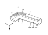
- FIG. 1 is a perspective view showing a first embodiment of a three-dimensional laminated wiring board according to the present invention.
- the three-dimensional laminated wiring board 1 shown in FIG. 1 is a board having a shape corresponding to the space in which it is arranged. Specifically, the three-dimensional laminated wiring board 1 has a three-dimensional solid shape for placement in a gap between the members. The three-dimensional laminated wiring board 1 is disposed, for example, at a corner portion in a housing of an electronic device (not shown), and is disposed in a gap with another component P disposed in the housing.
- the three-dimensional laminated wiring board 1 of the present embodiment has a truncated pyramid shape so as to cover the truncated pyramid portion P1 of another component P indicated by a broken line in FIG.
- the illustrated three-dimensional laminated wiring board 1 is a wiring board having three circuits. More specifically, the three-dimensional laminated wiring board 1 includes three types of antenna elements having different characteristics. Three external connection terminals 101, 102, and 103 are provided on the edge of the three-dimensional laminated wiring board 1. The external connection terminals 101, 102, and 103 are connected to lead wires (not shown) and other circuit boards.
- FIG. 2 is an exploded perspective view of the three-dimensional laminated wiring board shown in FIG.
- the three-dimensional laminated wiring board 1 has three three-dimensional wiring boards 11, 12, and 13 stacked on each other.
- Each of the three-dimensional wiring boards 11, 12, and 13 is also referred to as a first board 11, a second board 12, and a third board 13 in order from the top in FIG. 2.
- First, a configuration common to each of the three-dimensional wiring boards 11, 12, and 13 will be described by taking the first board 11 as a representative.
- the first substrate 11 includes an insulating film 111 and a conductor pattern 112.
- the insulating film 111 is a film made of a resin material.
- the resin material is a resin having thermoplasticity or thermosetting property. Examples of the resin material include PET (polyethylene terephthalate), PC (polycarbonate), polyimide, and PPS (polyphenylene sulfide).
- the insulating film 111 is formed so as to form a three-dimensional solid surface.
- the three-dimensional surface means a shape having a portion protruding from the surrounding portion, unlike a shape in which a flat film is simply bent along a fold line.
- the insulating film 111 of the present embodiment has a quadrangular frustum-shaped outer shape with an open bottom as a three-dimensional solid surface.
- the upper surface e of the truncated pyramidal insulating film 111 has four apexes a, b, c, d, that is, corners.
- the vertex a has a horizontal direction (diagonal horizontal direction X ′), a vertical direction (diagonal vertical direction Y ′), and a height.
- Surfaces f, g, and e facing in a three-dimensional direction independent of each other in direction Z are in contact.
- the apex a has a shape that passes through the surfaces f, g, and e and protrudes from an annular region surrounding the apex a.
- the upper surface e of the insulating film 111 of the present embodiment is in contact with the upper surface e in four directions and protrudes from the four inclined surfaces f, g, h, i surrounding the upper surface e.
- Such a three-dimensional solid surface of the insulating film 111 cannot be formed by simply bending a flat film along a fold line. For example, it is formed by heating and pressurizing a flat film using a molding die. . A method for forming the insulating film 111 will be described later.
- Three spacer protrusions 111j are provided on the insulating film 111 of the first substrate 11.
- the spacer protrusion 111j protrudes toward the second substrate 12 adjacent to the first substrate 11.
- the spacer protrusion 111j abuts against the second substrate 12 in a state where the first substrate 11 is overlaid on the second substrate 12. Accordingly, the distance between the portion of the first substrate 11 excluding the spacer protrusion 111j and the second substrate 12 is maintained.
- the insulating film 111 is provided with a protruding piece 111k protruding from the edge.
- the conductor pattern 112 of the first substrate 11 extends over the protruding piece 111k.
- the conductor pattern 112 on the protruding piece 111k constitutes the external connection terminal 101.
- the structure of the first substrate 11 described above is common to the second substrate 12 and the third substrate 13.
- the first substrate 11, the second substrate 12, and the third substrate 13 all have the same (substantially the same) three-dimensional solid surface.
- substrate 13 are laminated
- the spacer protrusion 111j of the first substrate 11 and the spacer protrusion 121j of the second substrate 12 are arranged at different positions. This prevents the spacer protrusion 111j of the first substrate 11 from entering the spacer protrusion 121j of the second substrate 12 when the first substrate 11 and the second substrate 12 overlap. More specifically, the spacer protrusion 111j of the first substrate 11 and the spacer protrusion 121j of the second substrate 12 are provided at positions that are point-symmetric with respect to the center of the upper surface e. Therefore, the 1st board
- the protruding piece 111k of the first substrate 11, the protruding piece 121k of the second substrate 12, and the protruding piece 131k of the third substrate 13 are arranged at positions that avoid overlapping each other. For this reason, in the three-dimensional laminated wiring board 1, the contact between the three external connection terminals 101, 102, 103 formed on the protruding pieces 111k, 121k, 131k is avoided. In addition, since each external connection terminal 101, 102, 103 is easily visually recognized, it is easy to connect with other components and lead wires.
- the first substrate 11, the second substrate 12, and the third substrate 13 in the present embodiment are formed with conductor patterns 112, 122, 132 having different shapes.
- the conductor pattern 112 is made of a conductive metal material. Examples of the metal material include copper, nickel, and gold. More specifically, the three-dimensional wiring boards 11, 12, and 13 are plated by the action of the plating catalyst on the insulating films 111, 121, and 131 formed so as to form a three-dimensional solid surface by printing the plating catalyst. Has a structured.
- the conductor patterns 112, 122, and 132 extend on the three-dimensional solid surfaces of the insulating films 111, 121, and 131, respectively, and extend to the protruding pieces 111k, 121k, and 131k.
- the conductor patterns 112, 122, 132 function as three antenna elements having the external connection terminals 101, 102, 103 as feed points. These antenna elements have different radiation characteristics depending on the shapes of the conductor patterns 112, 122, 132 arranged on the three-dimensional solid surface. For example, the conductor pattern 112 of the first substrate 11 and the conductor pattern 132 of the third substrate 13 have the same frequency characteristics as an antenna, but have different radiation distributions in space. Further, the conductor pattern 112 of the first substrate 11 and the conductor pattern 122 of the second substrate 12 have different frequency characteristics.
- the electronic device (not shown) to which the three-dimensional laminated wiring board 1 shown in FIG. 1 is attached uses three types of antennas selectively or simultaneously depending on the situation.
- three types of antennas can be built in a restricted space such as a corner of an electronic device.
- the first substrate 11, the second substrate 12, and the third substrate 13 all have the same three-dimensional solid surface and are laminated so that the three-dimensional solid surface is aligned. For this reason, positioning between the conductor patterns 112, 122, 132 during assembly is easy. In addition, fluctuations in characteristics caused by interaction and individual differences between products can be suppressed.
- FIG. 3 is a diagram for explaining a manufacturing process of the three-dimensional wiring board. From part (A) to part (B) in FIG. 3, as an example, the manufacturing process of the first substrate 11 is sequentially shown. However, the manufacturing process is the same for other substrates.
- a plating catalyst 1 ⁇ / b> C is printed on a resin insulating film 1 ⁇ / b> F spreading in a flat plate shape.
- the plating catalyst include a conductive polymer.
- an etching process and a base layer process may be implemented before printing of the catalyst 1C for plating.
- the insulating film 1F is heated and molded to form a three-dimensional solid surface by a molding die.
- the molding method include a vacuum molding method in which the insulating film 1F is sucked into the mold by air suction, a pressure molding method in which the insulating film 1F is pressed against the mold by air extrusion, and a mechanical stamping molding method. is there.
- the formed insulating film is subjected to chemical plating. Plating is performed by the action of the catalyst 1C for plating. A metal conductor pattern 112 is formed on the portion where the plating catalyst 1C is printed. In this way, the first substrate 11 is completed.
- the metal conductor pattern 112 is continuously formed without interruption at the apex and the ridgeline in the three-dimensional solid surface. Therefore, even when a complicated conductor pattern is formed on a three-dimensional solid surface, the connection reliability is high.
- the completed first substrate 11 is overlapped with the second substrate 12 and the third substrate 13 (see FIG. 2) manufactured in the same manner as the first substrate 11, and fixed with an adhesive or the like. In this way, the three-dimensional laminated wiring board 1 shown in FIG. 1 is completed.
- the shape similar to the three-dimensional solid surface shown in FIG. 2 can be formed, for example, by cutting a flat flexible substrate with a cut assuming a three-dimensional development view, and further joining the edges. Conceivable.
- the conductor pattern cannot be continued at the portion of the three-dimensional solid surface where the cuts are joined. Therefore, restrictions are imposed on the shape of the conductor pattern.
- the work of forming a three-dimensional solid surface is complicated and difficult to mechanize.
- the three-dimensional laminated wiring board 1 of this embodiment can position each layer by manufacturing each layer substantially simultaneously and combining them so as to match the three-dimensional solid surface. Therefore, a multilayer substrate circuit with high placement accuracy can be manufactured in a short time.
- the produced three-dimensional laminated wiring board 1 can arrange a complicated conductor pattern with high connection reliability at a high density on a three-dimensional solid surface adapted to a limited arrangement place such as an electronic device.
- the conductive pattern is formed only on the convex side surfaces, that is, one surface, of the first substrate 11, the second substrate 12, and the third substrate 13, respectively. Yes. Subsequently, a second embodiment of the present invention in which a conductor pattern is formed on the concave side surface or both surfaces of the substrate will be described.
- FIG. 4 is a cross-sectional view showing the structure of the three-dimensionally laminated wiring board according to the second embodiment.
- the conductive pattern 232 is provided on the convex side surface of the insulating film 231 as in the case of the first embodiment.
- the conductor pattern 212 is provided on the concave side surface of the insulating film 211.
- conductor patterns 222 and 223 are provided on both surfaces of the insulating film 221. In the figure, the thickness of the insulating film and the conductor pattern is exaggerated.
- the conductor pattern 212 of the first substrate 21 extends to the surface of the spacer protrusion 211j of the insulating film 211 and is in contact with the conductor pattern 222 of the second substrate 22. For this reason, one circuit is constituted by the conductor patterns 212 and 222 of the first substrate 21 and the second substrate 22 adjacent to each other.
- the conductor pattern 223 disposed on the surface of the second substrate 22 opposite to the conductor pattern 222 extends to the surface of the spacer protrusion 221j of the insulating film 221 and contacts the conductor pattern 232 of the third substrate 23. Yes.
- one circuit is constituted by the conductor patterns 233 and 232 of the second substrate 22 and the third substrate 23 adjacent to each other.
- the conductor patterns 223 and 232 may be bonded to each other using solder, a conductive adhesive, or the like.
- the three-dimensional laminated wiring board 2 it is possible to configure one circuit using the two boards 21 and 22 adjacent to each other.
- the spacer protrusions 211j and 221j hold the gap between the substrates, careless contact between the conductor patterns can be avoided in portions other than the spacer protrusions 211j and 221j.
- FIG. 5 is a sectional view showing the structure of the three-dimensionally laminated wiring board according to the third embodiment.
- the length along the horizontal direction of the spacer protrusion 311j formed on the insulating film 311 of the first substrate 31 is longer than the spacer protrusion 211j (see FIG. 4) in the second embodiment.
- a conductive pattern 312 spreading in a flat plate shape is provided on the surface of the spacer protrusion 311j.
- the insulating film 311 is provided with another conductive pattern 313 spreading in a flat plate shape at a position away from the conductive pattern 312.
- the conductor pattern is not provided on the convex side surface of the insulating film 321 of the second substrate 32.
- a conductor pattern 323 that extends in a flat plate shape including regions corresponding to the conductor patterns 312 and 313 of the first substrate 31 is provided.
- the first capacitor element C1 is formed by the conductor pattern 323 of the second substrate 32 and the conductor pattern 312 of the first substrate 31.
- the first capacitor element C1 has an electrostatic capacity according to the area in which the conductor patterns 323 and 312 serving as a pair of parallel plate electrodes overlap, and the thickness and dielectric constant of the insulating film 321.
- a second capacitor element C2 is formed by the conductor pattern 323 of the second substrate 32 and the other conductor pattern 313 of the first substrate 31.
- the second capacitor element C2 has a static capacity corresponding to the area where the conductor patterns 323 and 313 that form a pair of parallel plate electrodes overlap, the thickness and dielectric constant of the insulating film 321, and the height of the spacer protrusion 311j and the dielectric constant of air. It has electric capacity.
- the capacitance of the second capacitor element C2 can be adjusted by the height of the spacer protrusion 311j.
- FIG. 6 is a cross-sectional view showing a spacer protrusion portion of the three-dimensional laminated wiring board according to the fourth embodiment.
- the three-dimensional laminated wiring board 4 shown in FIG. 6 is obtained by stacking four three-dimensional wiring boards that are a first substrate 41, a second substrate 42, a third substrate 43, and a fourth substrate 44.
- the second substrate 42 and the third substrate 43 are disposed between the first substrate 41 and the fourth substrate 44.
- Each of the second substrate 42 and the third substrate 43 corresponds to an example of an intermediate three-dimensional wiring substrate according to the present invention.
- the second substrate 42 and the third substrate 43 are provided with holes 42h and 43h, respectively.
- the spacer protrusion 441j provided on the fourth substrate 44 penetrates the holes 42h and 43h and abuts against the first substrate 41.
- FIG. 7 is a perspective view showing a three-dimensional laminated wiring board according to the fifth embodiment.
- the three-dimensional laminated wiring board 5 shown in FIG. 7 is obtained by laminating a first substrate 51 and a second substrate 52 which are two three-dimensional wiring boards.
- the first substrate 51 and the second substrate 52 are respectively provided with insulating films 511 and 521 formed so as to form a three-dimensional solid surface.
- the three-dimensional solid surface of the insulating film 511 has surfaces f, g, f, g, which are directed to one vertex a in a three-dimensional direction independent of the horizontal direction X, the vertical direction Y, and the height direction Z. It is a triangular pyramid-shaped protrusion formed by contacting e. This shape is the same for the second substrate 42 disposed at the back (back side) of the first substrate 51.
- the first substrate 51 and the second substrate 52 are stacked so that the positions of the apexes a are aligned from the three-dimensional solid surface.
- a conductor pattern 512 that functions as an antenna element extends on the three-dimensional solid surface of the insulating film 511 of the first substrate 51.
- a conductor pattern (not shown) having a shape different from that of the first substrate 51 that functions as an antenna element also extends to the insulating film 521 of the second substrate 52 disposed inside the first substrate 51. .
- FIG. 8 is a perspective view showing an application example of the three-dimensional laminated wiring board of FIG.
- FIG. 8 shows a mobile communication terminal device 9 as an application example.
- An example of the mobile communication terminal device 9 is a smartphone.
- the mobile communication terminal device 9 has a thin rectangular parallelepiped shape, and the three-dimensional laminated wiring board 5 shown in FIG. 7 is mounted in the gap between the casing 91 and the built-in component 92 at the corner portion.
- the three-dimensional laminated wiring board 5 has two types of gaps in the limited space of the mobile communication terminal device 9 by the structure in which the first substrate 51 and the second substrate 52 forming a three-dimensional solid surface are laminated.
- An antenna can be built in.
- the conductor pattern constituting the antenna element is shown as an example of the conductor pattern referred to in the present invention.
- the present invention is not limited to this.
- the conductor pattern may constitute a general closed circuit.
- the conductor pattern may be one on which electronic components are mounted. Therefore, the three-dimensional laminated wiring board of the present invention may be applied to an apparatus that does not have a communication function, for example.
- the present invention is not limited to this.
- the number of three-dimensional wiring boards to be stacked may be five or more.
- a truncated pyramid shape or a pyramid shape is shown as an example of a shape forming a three-dimensional solid surface according to the present invention.
- the present invention is not limited to this, and may be spherical or cylindrical, for example.
- the three-dimensional wiring board may be one in which a portion forming a three-dimensional solid surface is provided on a part of a flat plate.
- holes 42h and 43hk are shown as examples of holes or notches in the present invention.
- the present invention is not limited to this, and the spacer protrusion may penetrate through a notch.
- the one having the protruding piece 111k is shown as an example of the three-dimensional wiring board referred to in the present invention.
- the present invention is not limited to this.
- the projection piece may be omitted.
- a board provided with conductor patterns having different shapes is shown.
- the present invention is not limited to this.
- a conductor pattern having the same shape may be provided as in the case of configuring an array antenna.
- the elements of the above-described embodiment may be used together or replaced.
- the conductor pattern of the second embodiment may be provided on both surfaces of each substrate in the three-dimensional multilayer wiring board of the first embodiment or the fifth embodiment, and the capacitor of the third embodiment may be formed. Good.
- Three-dimensional laminated wiring board 11 12, 13, 21, 22, 23, 31, 32, 33, 41, 42, 43, 44, 51, 52 Three-dimensional wiring board 101, 102, 103 External connection terminals 111j, 121j, 211j, 221j, 311j, 441j Spacer protrusions 111, 121, 131, 211, 221, 231, 311, 321, 511, 521 Insulating films 42h, 43h Holes 111k, 121k, 131k Protruding pieces 112, 122, 132, 212, 222, 223, 232, 233, 312, 313, 323, 512 Conductor pattern C1, C2 Capacitor element
Landscapes
- Engineering & Computer Science (AREA)
- Microelectronics & Electronic Packaging (AREA)
- Power Engineering (AREA)
- Manufacturing & Machinery (AREA)
- Production Of Multi-Layered Print Wiring Board (AREA)
- Structure Of Printed Boards (AREA)
- Combinations Of Printed Boards (AREA)
Description
本発明は、立体積層配線基板に関する。
筐体内の限定された空間に回路や配線を配置するため、例えば、フレキシブル基板を折線に沿って折り曲げて配置することが知られている。また、特許文献1には、銅箔を予め立体形成し、その銅箔とプリプレグシートを成形金型で加熱加圧して成形して得られる立体回路基板が開示されている。
フレキシブル基板は2次元の平板であり、曲がった平板を形成することはできるものの、例えば立体物のコーナーにおける縦横高さの3次元に広がる面をカバーするような回路や配線を形成することはできない。このことは、2次元の平面上に配置された銅箔をこの平面上の折線に沿って折り曲げる特許文献1の立体回路基板も同様である。例えば、特許文献1の技術において、銅箔に例えば突起を形成できたとしても、これに相応する形状のプリプレグシートとともに加熱加圧した場合、銅箔にしわや歪みが生じたり途中で切れたりするおそれがある。
本発明は上記問題点を解決し、制約された空間に収容可能で、かつ、信頼性の高い高密配線が可能な立体積層配線基板を提供することを目的とするものである。
上記目的を達成する本発明の立体積層配線基板は、複数の立体配線基板を有する立体積層配線基板であって、
上記複数の立体配線基板の少なくとも1つが、
3次元立体面を成すように形成された絶縁フィルムと、
上記3次元立体面上に延在する導体パターンとを有し、
上記複数の立体配線基板が積層されていることを特徴とする。
上記複数の立体配線基板の少なくとも1つが、
3次元立体面を成すように形成された絶縁フィルムと、
上記3次元立体面上に延在する導体パターンとを有し、
上記複数の立体配線基板が積層されていることを特徴とする。
本発明の立体積層配線基板では、3次元立体面を有する立体配線基板が積層されるため、例えば電子機器のコーナー部分のような制約された空間に収容可能な、信頼性の高い高密配線が可能となる。
ここで、上記本発明の立体積層配線基板において、上記複数の立体配線基板は、いずれも略同一の3次元立体面を有し、これら略同一の3次元立体面が揃うように積層されたものであってもよい。
各立体配線基板の3次元立体面に延在する導体パターンが入れ子状に配置される。したがって、3次元立体面を利用してより高密度な配線が可能となる。
また、上記本発明の立体積層配線基板において、上記複数の立体配線基板のそれぞれは、互いに異なる形状の導体パターンが設けられたものであってもよい。
複数の立体配線基板のそれぞれに、異なる形状の導体パターンによって、例えば複数のアンテナ素子を有するアンテナのような異なる特性を有する素子を構成することができる。したがって、形状が制約された空間に複数の機能を収容することができる。
また、上記本発明の立体積層配線基板において、上記立体配線基板は、この立体配線基板に隣接する別の立体配線基板に突き当たることでこの別の立体配線基板との間隔を維持するスペーサ突起が形成されたものであってもよい。
スペーサ突起により、隣接した立体配線基板同士に間隔をあけることができるので、絶縁フィルムの表裏両面に導体パターンを互いに短絡することなく配置することができる。
また、上記本発明の立体積層配線基板が3つ以上の立体配線基板を有するものであって、
上記3つ以上の立体配線基板のうち中間に配置された中間立体配線基板には孔又は切欠きが設けられ、
上記スペーサ突起が、上記孔又は切欠きを貫通して上記中間立体配線基板を挟んだ反対側に配置された別の立体配線基板に突き当たるものであってもよい。
上記3つ以上の立体配線基板のうち中間に配置された中間立体配線基板には孔又は切欠きが設けられ、
上記スペーサ突起が、上記孔又は切欠きを貫通して上記中間立体配線基板を挟んだ反対側に配置された別の立体配線基板に突き当たるものであってもよい。
また、上記本発明の立体積層配線基板において、上記立体配線基板の導体パターンが、上記スペーサ突起の表面に延び、この別の立体配線基板の導体パターンと接触したものであってもよい。
スペーサ突起を介して、互いに隣接した2枚の立体配線基板に設けられた導体パターンを電気的に接続することができる。したがって、2枚の立体配線基板に設けられた導体パターンで1つの回路を形成することができる。
また、上記本発明の立体積層配線基板において、上記複数の立体配線板のうちの互いに隣接した2枚の立体配線基板の導体パターンが、コンデンサ素子を形成する平行平板電極を形成したものであってもよい。
スペーサ突起の高さによって静電容量を設定可能なコンデンサ素子が実現する。
また、上記本発明の立体積層配線基板において、上記複数の立体配線基板のそれぞれの縁には、互いに重なりを避けた位置に突出した突出片が設けられ、この複数の立体配線基板それぞれの導体パターンがこの複数の立体配線基板それぞれの突出片上に延びていてもよい。
突出片に設けられた導体パターンを立体配線基板の外部接続端子として利用することができる。このとき、外部接続端子同士の接触が避けられる。また、各外部接続端子の視認性が高いので接続作業が容易である。
また、上記本発明の立体積層配線基板において、上記導体パターンは、めっき用触媒がプリントされて3次元立体面を成すように成形された絶縁フィルム上に、このめっき用触媒の作用によりめっきされたものであってもよい。
めっき用触媒がプリントされて成形された絶縁フィルム上にめっきがなされた立体積層配線基板では、3次元立体面を成す面と面との境界である稜線や頂点に亘り、導体パターンが途切れなく連続して形成される。したがって、3次元立体面に延在する複雑な導体パターンの形成の信頼性が高い。
以上説明したように、本発明によれば、制約された空間に収容可能で、かつ、信頼性の高い高密配線が可能な立体積層配線基板が実現する。
以下図面を参照して本発明の実施の形態を説明する。
図1は、本発明の立体積層配線基板の第1実施形態を示す斜視図である。
図1に示す立体積層配線基板1は、配置される空間に相応した形状を有する基板である。具体的には、立体積層配線基板1は、部材と部材の間の隙間に配置するための3次元立体形状を有する。立体積層配線基板1は、例えば図示しない電子機器の筐体内のコーナー部分に配置され、筐体内に配置される他の部品Pとの隙間に配置される。本実施形態の立体積層配線基板1は、図1に破線で示す他の部品Pの、角錐台部分P1に被さるよう、角錐台状の外形を有する。
例示された立体積層配線基板1は、3つの回路を有する配線基板である。より詳細には、立体積層配線基板1は、特性が互いに異なる3種類のアンテナ素子を備えている。立体積層配線基板1の縁には、3つの外部接続端子101,102,103が設けられている。外部接続端子101,102,103には、図示しないリード線や別の回路基板が接続される。
図2は、図1に示す立体積層配線基板の分解斜視図である。
図2に示すように、立体積層配線基板1は、互いに積み重ねられた3つの立体配線基板11,12,13を有する。なお、立体配線基板11,12,13のそれぞれを、図2における上から順に、第1基板11、第2基板12、および第3基板13とも称する。まず、立体配線基板11,12,13のそれぞれに共通の構成を、第1基板11を代表として採り上げ説明する。
第1基板11は、絶縁フィルム111および導体パターン112を備えている。
絶縁フィルム111は、樹脂材料からなるフィルムである。樹脂材料は、熱可塑性または熱硬化性を有する樹脂である。樹脂材料は、例えば、PET(ポリエチレンテレフタラート)、PC(ポリカーボネート)、ポリイミド、およびPPS(ポリフェニレンスルフィド)が挙げられる。絶縁フィルム111は、3次元立体面を成すように形成されている。ここで、3次元立体面とは、平板状のフィルムが単に折線に沿って折り曲げられた形状とは異なり、取り巻き部分よりも突出した部分を有する形状を意味している。本実施形態の絶縁フィルム111は、3次元立体面として、底面が開口した四角錐台状の外形を有する。より詳細には、四角錐台状の絶縁フィルム111の上面eは4つの頂点a,b,c,d、すなわち角を有している。4つの頂点a,b,c,dのうちの1つの頂点aに着目すると、この頂点aには、横方向(斜め横方向X’)、縦方向(斜め縦方向Y’)、および高さ方向Zの互いに独立した3次元の方向に向いた面f,g,eが接している。頂点aは、面f,g,eを通りこの頂点aを取り巻いた環状の領域に対して突出した形状となっている。これと同様のことが、残りの3つの頂点b,c,dについてもいえる。また、本実施形態の絶縁フィルム111の上面eに着目すると、この上面eは、上面eに四方で接し、上面eを取り巻く4つの斜面f,g,h,iよりも突出しているといえる。このような絶縁フィルム111の3次元立体面は、単に平板状のフィルムを折線に沿って折り曲げることでは形成できず、例えば、成型用の型を用い平板状のフィルムを加熱加圧することで形成する。絶縁フィルム111の形成方法については、後述する。
第1基板11の絶縁フィルム111には、3つのスペーサ突起111jが設けられている。スペーサ突起111jは、第1基板11が隣接する第2基板12に向かって突出している。スペーサ突起111jは、第1基板11が第2基板12に重ねられた状態で、第2基板12に突き当たる。これによって、第1基板11のスペーサ突起111jを除いた部分と第2基板12との間隔が維持される。
また、絶縁フィルム111には、縁から突出した突出片111kが設けられている。第1基板11の導体パターン112は、突出片111kの上まで延びている。突出片111k上の導体パターン112が、外部接続端子101を構成している。
以上説明した第1基板11の構造は、第2基板12および第3基板13についても共通である。第1基板11、第2基板12および第3基板13は、いずれも同様(ほぼ同一)の3次元立体面を有している。そして、第1基板11、第2基板12および第3基板13は、図1に示す状態では、3次元立体面が揃うように積層されている。
第1基板11のスペーサ突起111jと第2基板12のスペーサ突起121jとは異なる位置に配置されている。これによって、第1基板11と第2基板12が重なったときに、第2基板12のスペーサ突起121jに第1基板11のスペーサ突起111jが入り込むことが防止される。より詳細には、第1基板11のスペーサ突起111jと第2基板12のスペーサ突起121jとは、上面eの中心に対して点対称の位置に設けられている。したがって、第1基板11と第2基板12とは、共通の成型用型によって形成し、反対向きの姿勢をすることで実現できる。
第1基板11の突出片111k、第2基板12の突出片121k、および第3基板13の突出片131kは、互いに重なりを避けた位置に配置されている。このため、立体積層配線基板1では、突出片111k,121k,131k上に構成される3つの外部接続端子101,102,103同士の接触が避けられる。また、各外部接続端子101,102,103が容易に視認されるので、他の部品やリード線との接続作業が容易である。
本実施形態における第1基板11、第2基板12および第3基板13は、互いに異なる形状の導体パターン112,122,132が形成されている。導体パターン112は、導電性の金属材料で形成されている。金属材料としては、例えば銅、ニッケル、金が挙げられる。より詳細には、立体配線基板11,12,13は、めっき用触媒がプリントされて3次元立体面を成すように成形された絶縁フィルム111,121,131上に、めっき用触媒の作用によりめっきされた構造を有する。導体パターン112,122,132は、絶縁フィルム111,121,131の3次元立体面上にそれぞれ延在し、突出片111k,121k,131kまで延びている。導体パターン112,122,132は、外部接続端子101,102,103を給電点とする3つのアンテナ素子として機能する。これらのアンテナ素子は、3次元立体面に配置された導体パターン112,122,132の形状に応じて、互いに異なる放射特性を有している。例えば、第1基板11の導体パターン112と、第3基板13の導体パターン132とは、アンテナとして同様の周波数特性を有するが、空間内における放射分布が異なる。また、第1基板11の導体パターン112と、第2基板12の導体パターン122とは、周波数特性が異なる。
図1に示す立体積層配線基板1が取り付けられた図示しない電子機器は、状況に応じて3種類のアンテナを選択的あるいは同時に使用する。立体積層配線基板1を用いることで、例えば電子機器のコーナーのような制約された空間に3種類のアンテナが内蔵できる。
本実施形態における、第1基板11、第2基板12および第3基板13は、いずれも同様の3次元立体面を有し、3次元立体面が揃うように積層されている。このため、組立時における導体パターン112,122,132の相互間の位置決めが容易である。また、相互作用に起因する特性の変動や、製品ごとの個体差が抑えられる。
図3は、立体配線基板の製造工程を説明する図である。図3のパート(A)からパート(B)までには、例として第1基板11の製造工程が順に示されている。ただし、製造工程は他の基板も同様である。
第1基板11を製造するには、まず、図3のパート(A)に示すように、平板状に広がる樹脂製の絶縁フィルム1F上に、めっき用触媒1Cをプリントする。めっき用触媒としては、例えば、導電性ポリマが挙げられる。なお、めっき用触媒1Cのプリント前に、エッチング処理や下地層処理が実施されてもよい。
次に、図3のパート(B)に示すように、絶縁フィルム1Fを加熱するとともに、成型用型によって3次元立体面を成すように成形する。成型の方法としては、例えば、空気の吸引によって絶縁フィルム1Fを型に吸い付ける真空成型法や、空気の押出しによって絶縁フィルム1Fを型に押し当てる圧空成形法、機械的な型押し成形法等がある。
次に、図3のパート(C)に示すように、成形された絶縁フィルムに化学めっき処理を施す。めっき用触媒1Cの作用により、めっきがなされる。めっき用触媒1Cがプリントされた部分に金属製の導体パターン112が形成される。このようにして、第1基板11が完成する。
めっき処理は、絶縁フィルム1Fの成形後に実施されるので、金属の導体パターン112が3次元立体面における頂点や稜線において途切れることなく連続して形成される。したがって、3次元立体面上に複雑な導体パターンを形成した場合でも、接続の信頼性が高い。
最後に、完成した第1基板11を、この第1基板11と同様に製造した第2基板12、第3基板13(図2参照)と重ね、接着材等により固定する。このようにして、図1に示す立体積層配線基板1が完成する。
ところで、図2に示す3次元立体面に類似した形状は、例えば、平板状のフレキシブル基板に、立体の展開図を想定した切り込みを入れて折り曲げ、さらに縁を継貼りすることにより形成することが考えられる。しかし、この場合には、3次元立体面のうち、切り込みを継ぎ貼りした部分で導体パターンを連続させることはできない。したがって、導体パターンの形状に制約が生じる。また、3次元立体面の形成作業が複雑であり、機械化が困難である。
また、射出成型等により、図2に示す3次元立体面に類似した形状を製造しようとした場合には、形成される基板の厚みを、射出成型可能な厚みとすることが必要となる。したがって、物品の隙間のような狭い空間に積層配置することができない。
また、3次元立体面を有しないフレキシブル基板において、導体パターンを多層配置しようとした場合には、導体パターンの形成と絶縁層の形成を交互に繰り返す必要がある。したがって、多層構造の形成に時間がかかる。これに対し、本実施形態の立体積層配線基板1は、各層の形成を略同時に製造し、3次元立体面を合わせるように組み合わせることで各層間の位置決めを行うことができる。したがって、短時間で配置精度の高い多層基板回路が製造できる。
製造された立体積層配線基板1は、電子機器等の限定された配置場所に適応した3次元立体面に、接続信頼性の高い複雑な導体パターンを高密度に配置することができる。
[第2実施形態]
上述した第1実施形態の立体積層配線基板1は、第1基板11、第2基板12および第3基板13のそれぞれの上を向いた凸側面、つまり一方の面にのみ導体パターンが形成されている。続いて、基板の凹側面、または両面に導体パターンが形成された本発明の第2実施形態について説明する。
上述した第1実施形態の立体積層配線基板1は、第1基板11、第2基板12および第3基板13のそれぞれの上を向いた凸側面、つまり一方の面にのみ導体パターンが形成されている。続いて、基板の凹側面、または両面に導体パターンが形成された本発明の第2実施形態について説明する。
図4は、第2実施形態の立体積層配線基板の構造を示す断面図である。
図4に示す立体積層配線基板2は、第1基板21、第2基板22、および第3基板23を備えている。一番下の第3基板23では、第1実施形態の場合と同様、絶縁フィルム231の凸側面に導体パターン232が設けられている。しかし、一番上の第1基板21では、絶縁フィルム211の凹側面に導体パターン212が設けられている。また、第2基板22では、絶縁フィルム221の両面に導体パターン222,223が設けられている。なお、図では、絶縁フィルムや導体パターンの厚みが誇張して示されている。
第1基板21の導体パターン212は、絶縁フィルム211のスペーサ突起211jの表面に延び、第2基板22の導体パターン222と接触している。このため、互いに隣接する第1基板21および第2基板22の導体パターン212,222によって、1つの回路が構成される。
また、第2基板22の、上記導体パターン222とは反対の面に配置された導体パターン223は、絶縁フィルム221のスペーサ突起221jの表面に延び、第3基板23の導体パターン232と接触している。このため、互いに隣接する第2基板22および第3基板23の導体パターン233,232によって、1つの回路が構成されている。なお、導体パターン223,232は、半田、導電性接着剤等を用いて互いに接合してもよい。
このように、立体積層配線基板2によれば、1つの回路を、互いに隣接する2つの基板21,22を利用して構成することが可能である。また、図4において明らかなように、スペーサ突起211j,221jが基板同士の隙間を保持しているため、スペーサ突起211j,221j以外の部分では、導体パターン同士の不用意な接触が避けられる。
[第3実施形態]
続いて、導体パターンによってコンデンサ素子が形成された、本発明の第3実施形態について説明する。
続いて、導体パターンによってコンデンサ素子が形成された、本発明の第3実施形態について説明する。
図5は、第3実施形態の立体積層配線基板の構造を示す断面図である。
図5に示す立体積層配線基板3は、第1基板31の絶縁フィルム311に形成されたスペーサ突起311jの水平方向に沿った長さが、第2実施形態におけるスペーサ突起211j(図4参照)よりも大きい。そして、スペーサ突起311jの表面には、平板状に広がった導体パターン312が設けられている。また、絶縁フィルム311には、上記導体パターン312とは離れた位置に、別の、平板状に広がった導体パターン313が設けられている。
第2基板32の絶縁フィルム321の凸側面には、導体パターンは設けられていない。第2基板32の凹側面には、第1基板31の導体パターン312,313と相応する領域を含んで平板状に広がった導体パターン323が設けられている。
第2基板32の導体パターン323と、第1基板31の導体パターン312によって、第1のコンデンサ素子C1が形成されている。第1のコンデンサ素子C1は、一対の平行平板電極となる導体パターン323,312が重なる面積、ならびに絶縁フィルム321の厚みおよび誘電率に応じた静電容量を有する。また、第2基板32の導体パターン323と、第1基板31のもう一つの導体パターン313によって、第2のコンデンサ素子C2が形成されている。第2のコンデンサ素子C2は、一対の平行平板電極となる導体パターン323,313が重なる面積、絶縁フィルム321の厚みおよび誘電率、ならびに、スペーサ突起311jの高さおよび空気の誘電率に応じた静電容量を有する。第2のコンデンサ素子C2は、スペーサ突起311jの高さによって、静電容量の調整が可能である。
[第4実施形態]
続いて、本発明の第4実施形態について説明する。
続いて、本発明の第4実施形態について説明する。
図6は、第4実施形態の立体積層配線基板のスペーサ突起部分を示す断面図である。
図6に示す立体積層配線基板4は、第1基板41、第2基板42、第3基板43、および第4基板44である4つの立体配線基板が積層されたものである。第2基板42および第3基板43は、第1基板41および第4基板44の中間に配置されている。第2基板42および第3基板43のそれぞれは、本発明にいう中間立体配線基板の一例に相当する。
第2基板42および第3基板43には、孔42h,43hがそれぞれ設けられている。第4基板44に設けられたスペーサ突起441jは、孔42h,43hを貫通して、第1基板41に突き当たっている。
[第5実施形態]
続いて、本発明の第5実施形態について説明する。
続いて、本発明の第5実施形態について説明する。
図7は、第5実施形態の立体積層配線基板を示す斜視図である。
図7に示す立体積層配線基板5は、2つの立体配線基板である第1基板51および第2基板52が積層されたものである。第1基板51および第2基板52は、3次元立体面を成すように形成された絶縁フィルム511,521をそれぞれ備えている。より詳細には、絶縁フィルム511の3次元立体面は、1つの頂点aに、横方向X、縦方向Y、および高さ方向Zの互いに独立した3次元の方向に向いた面f,g,eが接してなる三角錐状の突形状である。この形状は、第1基板51の奥(裏側)に配置された第2基板42についても同様である。第1基板51および第2基板52は、3次元立体面より具体的には頂点aの位置が揃うように積層されている。第1基板51の絶縁フィルム511の3次元立体面上には、アンテナ素子として機能する導体パターン512が延在している。また、第1基板51の内側に配置された第2基板52の絶縁フィルム521にも、アンテナ素子として機能する、第1基板51のものとは異なる形状の図示しない導体パターンが延在している。
図8は、図7の立体積層配線基板の応用例を示す斜視図である。
図8には、応用例として携帯通信端末装置9が示されている。携帯通信端末装置9の一例は、スマートフォンである。携帯通信端末装置9は、薄い直方体状であり、コーナー部分の、筐体91と内蔵部品92との隙間には、図7に示す立体積層配線基板5が搭載されている。立体積層配線基板5は、図7に示すように3次元立体面を成す第1基板51および第2基板52が積層された構造によって、携帯通信端末装置9の限られた隙間に、2種類のアンテナを内蔵させることができる。
なお、上述した実施形態には、本発明にいう導体パターンの例として、アンテナ素子を構成する導体パターンが示されている。ただし、本発明はこれに限られるものではなく、例えば、導体パターンは、一般的な閉回路を構成するものであってもよい。また、導体パターンには、電子部品が搭載されたものであってもよい。したがって、本発明の立体積層配線基板は、例えば通信機能を有しない装置に適用されるものであってもよい。
また、上述した実施形態には、本発明にいう立体積層配線基板の例として、2つから4つの基板が積層された構造が示されている。ただし、本発明はこれに限られるものではなく、例えば、積層される立体配線基板の数は、5以上であってもよい。
また、上述した実施形態には、本発明にいう3次元立体面を成す形状の例として、角錐台状や角錐状のものが示されている。ただし、本発明はこれに限られるものではなく、例えば、球状や円柱状であってもよい。また、立体配線基板は、平板状の一部に3次元立体面を成す部分が設けられたものであってもよい。
また、上述した実施形態には、本発明にいう孔又は切欠きの例として、孔42h、43hkが示されている。ただし、本発明はこれに限られるものではなく、スペーサ突起が貫通するのは切欠きであってもよい。
また、上述した実施形態には、本発明にいう立体配線基板の例として、突出片111kを有するものが示されている。ただし、本発明はこれに限られるものではなく、例えば、突出片がないものであってもよい。
また、上述した実施形態には、本発明にいう複数の立体配線基板の例として、互いに異なる形状の導体パターンが設けられた基板が示されている。ただし、本発明はこれに限られるものではなく、例えば、アレイアンテナを構成する場合のように、同じ形状の導体パターンが設けられたものであってもよい。
また、本発明にいう立体積層配線基板の例として、上述した実施形態の要素を併用、入替えしたものであってもよい。例えば、第1実施形態または第5実施形態の立体積層配線基板における各基板の両面に、第2実施形態の導体パターンが設けられてもよく、また、第3実施形態のコンデンサが形成されてもよい。
1,2,3,4,5 立体積層配線基板
11,12,13,21,22,23,31,32,33,41,42,43,44,51,52 立体配線基板
101,102,103 外部接続端子
111j,121j,211j,221j,311j,441j スペーサ突起
111,121,131,211,221,231,311,321,511,521 絶縁フィルム
42h,43h 穴
111k,121k,131k 突出片
112,122,132,212,222,223,232,233,312,313,323,512 導体パターン
C1,C2 コンデンサ素子
11,12,13,21,22,23,31,32,33,41,42,43,44,51,52 立体配線基板
101,102,103 外部接続端子
111j,121j,211j,221j,311j,441j スペーサ突起
111,121,131,211,221,231,311,321,511,521 絶縁フィルム
42h,43h 穴
111k,121k,131k 突出片
112,122,132,212,222,223,232,233,312,313,323,512 導体パターン
C1,C2 コンデンサ素子
Claims (9)
- 複数の立体配線基板を有する立体積層配線基板であって、
前記複数の立体配線基板のそれぞれが、
3次元立体面を成すように形成された絶縁フィルムと、
前記3次元立体面上に延在する導体パターンとを有し、
前記複数の立体配線基板が積層されていることを特徴とする立体積層配線基板。 - 前記複数の立体配線基板は、いずれも略同一の3次元立体面を有し、これら略同一の3次元立体面が揃うように積層されたものであることを特徴とする請求項1記載の立体積層配線基板。
- 前記複数の立体配線基板のそれぞれは、互いに異なる形状の導体パターンが設けられたものであることを特徴とする請求項1または2記載の立体積層配線基板。
- 前記立体配線基板は、当該立体積層配線基板を構成する別の立体配線基板に突き当たることで該別の立体配線基板との間隔を維持するスペーサ突起が形成されたものであることを特徴とする請求項1から3のうちのいずれか1項記載の立体積層配線基板。
- 当該立体積層配線基板が3つ以上の立体配線基板を有するものであって、
前記3つ以上の立体配線基板のうち中間に配置された中間立体配線基板には孔又は切欠きが設けられ、
前記スペーサ突起が、前記孔又は切欠きを貫通して前記中間立体配線基板を挟んだ反対側に配置された別の立体配線基板に突き当たるものであることを特徴とする請求項1から4のうちのいずれか1項記載の立体積層配線基板。 - 前記立体配線基板の導体パターンが、前記スペーサ突起の表面に延び、該別の立体配線基板の導体パターンと接触したものであることを特徴とする請求項4記載の立体積層配線基板。
- 前記複数の立体配線板のうちの互いに隣接した2枚の立体配線基板の導体パターンが、コンデンサ素子を形成する平行平板電極を形成したものであることを特徴とする請求項4記載の立体積層配線基板。
- 前記複数の立体配線基板のそれぞれの縁には、互いに重なりを避けた位置に突出した突出片が設けられ、該複数の立体配線基板それぞれの導体パターンが該複数の立体配線基板それぞれの突出片上に延びていることを特徴とする請求項1から7のうちのいずれか1項記載の立体積層配線基板。
- 前記導体パターンは、めっき用触媒がプリントされて3次元立体面を成すように成形された絶縁フィルム上に、該めっき用触媒の作用によりめっきされたものであることを特徴とする請求項1から8のうちのいずれか1項記載の立体積層配線基板。
Priority Applications (4)
| Application Number | Priority Date | Filing Date | Title |
|---|---|---|---|
| EP13758350.6A EP2825004A4 (en) | 2012-03-06 | 2013-01-31 | THREE-DIMENSIONAL LAMINATED WIRING SUPPLEMENT |
| CN201380012964.1A CN104145536B (zh) | 2012-03-06 | 2013-01-31 | 立体层叠布线基板 |
| IN7164DEN2014 IN2014DN07164A (ja) | 2012-03-06 | 2014-08-26 | |
| US14/472,976 US9894758B2 (en) | 2012-03-06 | 2014-08-29 | Three-dimensional laminated wiring substrate |
Applications Claiming Priority (2)
| Application Number | Priority Date | Filing Date | Title |
|---|---|---|---|
| JP2012-049413 | 2012-03-06 | ||
| JP2012049413A JP5973190B2 (ja) | 2012-03-06 | 2012-03-06 | 立体積層配線基板 |
Related Child Applications (1)
| Application Number | Title | Priority Date | Filing Date |
|---|---|---|---|
| US14/472,976 Continuation US9894758B2 (en) | 2012-03-06 | 2014-08-29 | Three-dimensional laminated wiring substrate |
Publications (1)
| Publication Number | Publication Date |
|---|---|
| WO2013132930A1 true WO2013132930A1 (ja) | 2013-09-12 |
Family
ID=49116416
Family Applications (1)
| Application Number | Title | Priority Date | Filing Date |
|---|---|---|---|
| PCT/JP2013/052182 Ceased WO2013132930A1 (ja) | 2012-03-06 | 2013-01-31 | 立体積層配線基板 |
Country Status (7)
| Country | Link |
|---|---|
| US (1) | US9894758B2 (ja) |
| EP (1) | EP2825004A4 (ja) |
| JP (1) | JP5973190B2 (ja) |
| CN (1) | CN104145536B (ja) |
| IN (1) | IN2014DN07164A (ja) |
| TW (1) | TWM470479U (ja) |
| WO (1) | WO2013132930A1 (ja) |
Cited By (3)
| Publication number | Priority date | Publication date | Assignee | Title |
|---|---|---|---|---|
| JP6014792B1 (ja) * | 2015-06-24 | 2016-10-25 | 株式会社メイコー | 立体配線基板の製造方法、立体配線基板、立体配線基板用基材 |
| WO2016208090A1 (ja) * | 2015-06-24 | 2016-12-29 | 株式会社メイコー | 立体配線基板の製造方法、立体配線基板、立体配線基板用基材 |
| JP6169304B1 (ja) * | 2016-07-07 | 2017-07-26 | 株式会社メイコー | 立体配線基板、立体配線基板の製造方法、立体配線基板用基材 |
Families Citing this family (12)
| Publication number | Priority date | Publication date | Assignee | Title |
|---|---|---|---|---|
| TWI527306B (zh) * | 2013-12-09 | 2016-03-21 | 矽品精密工業股份有限公司 | 電子組件 |
| US20150257278A1 (en) * | 2014-03-06 | 2015-09-10 | Tactotek Oy | Method for manufacturing electronic products, related arrangement and product |
| JP2016129214A (ja) * | 2015-01-05 | 2016-07-14 | みさこ 俵山 | 立体パーツ同士を組み合わせ立体配置可能な立体基板 |
| TWI557533B (zh) | 2015-02-10 | 2016-11-11 | 宏碁股份有限公司 | 電子裝置 |
| CN105990638B (zh) * | 2015-02-16 | 2018-11-02 | 宏碁股份有限公司 | 电子装置 |
| CN107404797B (zh) * | 2016-05-18 | 2019-06-11 | 庆鼎精密电子(淮安)有限公司 | 具有段差结构的多层电路板及其制作方法 |
| CN105977364A (zh) * | 2016-07-20 | 2016-09-28 | 广州硅能照明有限公司 | 多层led光引擎结构及其加工方法 |
| JP6806522B2 (ja) * | 2016-10-20 | 2021-01-06 | 矢崎総業株式会社 | 回路体、及び、樹脂成形体 |
| CN110112538B (zh) * | 2019-04-18 | 2024-09-24 | 北京Abb电气传动系统有限公司 | 天线装置 |
| TWI726747B (zh) * | 2020-06-16 | 2021-05-01 | 國立臺灣科技大學 | 線路基板及其製造方法 |
| US20220310778A1 (en) * | 2021-03-26 | 2022-09-29 | Taiwan Semiconductor Manufacturing Company Limited | Semiconductor arrangement and method of making |
| JP7518957B1 (ja) | 2023-11-29 | 2024-07-18 | 太陽ホールディングス株式会社 | 導電パターンを有する構造体 |
Citations (8)
| Publication number | Priority date | Publication date | Assignee | Title |
|---|---|---|---|---|
| JPS5834790U (ja) * | 1981-08-29 | 1983-03-07 | 株式会社ユ−シン | プリント基板の多段固定構造 |
| JPH01169083U (ja) * | 1988-05-18 | 1989-11-29 | ||
| JPH09266368A (ja) | 1996-03-28 | 1997-10-07 | Mitsubishi Electric Corp | 立体回路基板の製造方法 |
| JP2007123940A (ja) * | 2003-06-27 | 2007-05-17 | Tdk Corp | コンデンサを内蔵した基板およびその製造方法 |
| JP2009164340A (ja) * | 2008-01-07 | 2009-07-23 | Du Pont Toray Co Ltd | 立体回路基板及びその製造方法 |
| JP2010027724A (ja) * | 2008-07-16 | 2010-02-04 | Denso Wave Inc | 基板用スペーサ及び基板間連結構造 |
| JP2010140638A (ja) * | 2007-03-29 | 2010-06-24 | Citizen Holdings Co Ltd | 積層基板の電極端子接続構造 |
| JP2012036339A (ja) * | 2010-08-10 | 2012-02-23 | Hitachi Chem Co Ltd | 樹脂組成物、樹脂硬化物、配線板及び配線板の製造方法 |
Family Cites Families (10)
| Publication number | Priority date | Publication date | Assignee | Title |
|---|---|---|---|---|
| JPS5834790A (ja) | 1981-08-25 | 1983-03-01 | ファナック株式会社 | 波状薄物ワ−ク吸着具 |
| DE8715925U1 (de) | 1987-12-02 | 1988-02-11 | Kiekert AG, 42579 Heiligenhaus | Kraftfahrzeugtürverschluß mit Schließkeil und Schloß |
| GB2255451B (en) * | 1991-05-03 | 1995-01-25 | Marconi Gec Ltd | Ceramic three dimensional electronic structures |
| US5264061A (en) * | 1992-10-22 | 1993-11-23 | Motorola, Inc. | Method of forming a three-dimensional printed circuit assembly |
| JPH07170077A (ja) * | 1993-12-16 | 1995-07-04 | Hitachi Cable Ltd | 射出成形回路部品の製造方法 |
| JPH10140638A (ja) | 1996-11-07 | 1998-05-26 | Act:Kk | 汚物処理装置 |
| US6525414B2 (en) * | 1997-09-16 | 2003-02-25 | Matsushita Electric Industrial Co., Ltd. | Semiconductor device including a wiring board and semiconductor elements mounted thereon |
| JP2001257476A (ja) * | 2000-03-14 | 2001-09-21 | Oki Printed Circuit Kk | 多層配線基板及びその製造方法 |
| TW507514B (en) * | 2000-11-27 | 2002-10-21 | Matsushita Electric Works Ltd | Multilayer circuit board and method of manufacturing the same |
| CN101730397B (zh) * | 2008-10-27 | 2012-05-02 | 欣兴电子股份有限公司 | 多层立体线路的结构及其制作方法 |
-
2012
- 2012-03-06 JP JP2012049413A patent/JP5973190B2/ja not_active Expired - Fee Related
-
2013
- 2013-01-31 WO PCT/JP2013/052182 patent/WO2013132930A1/ja not_active Ceased
- 2013-01-31 CN CN201380012964.1A patent/CN104145536B/zh active Active
- 2013-01-31 EP EP13758350.6A patent/EP2825004A4/en not_active Withdrawn
- 2013-02-01 TW TW102202249U patent/TWM470479U/zh not_active IP Right Cessation
-
2014
- 2014-08-26 IN IN7164DEN2014 patent/IN2014DN07164A/en unknown
- 2014-08-29 US US14/472,976 patent/US9894758B2/en not_active Expired - Fee Related
Patent Citations (8)
| Publication number | Priority date | Publication date | Assignee | Title |
|---|---|---|---|---|
| JPS5834790U (ja) * | 1981-08-29 | 1983-03-07 | 株式会社ユ−シン | プリント基板の多段固定構造 |
| JPH01169083U (ja) * | 1988-05-18 | 1989-11-29 | ||
| JPH09266368A (ja) | 1996-03-28 | 1997-10-07 | Mitsubishi Electric Corp | 立体回路基板の製造方法 |
| JP2007123940A (ja) * | 2003-06-27 | 2007-05-17 | Tdk Corp | コンデンサを内蔵した基板およびその製造方法 |
| JP2010140638A (ja) * | 2007-03-29 | 2010-06-24 | Citizen Holdings Co Ltd | 積層基板の電極端子接続構造 |
| JP2009164340A (ja) * | 2008-01-07 | 2009-07-23 | Du Pont Toray Co Ltd | 立体回路基板及びその製造方法 |
| JP2010027724A (ja) * | 2008-07-16 | 2010-02-04 | Denso Wave Inc | 基板用スペーサ及び基板間連結構造 |
| JP2012036339A (ja) * | 2010-08-10 | 2012-02-23 | Hitachi Chem Co Ltd | 樹脂組成物、樹脂硬化物、配線板及び配線板の製造方法 |
Non-Patent Citations (1)
| Title |
|---|
| See also references of EP2825004A4 * |
Cited By (9)
| Publication number | Priority date | Publication date | Assignee | Title |
|---|---|---|---|---|
| JP6014792B1 (ja) * | 2015-06-24 | 2016-10-25 | 株式会社メイコー | 立体配線基板の製造方法、立体配線基板、立体配線基板用基材 |
| WO2016208093A1 (ja) * | 2015-06-24 | 2016-12-29 | 株式会社メイコー | 立体配線基板、及び立体配線基板の製造方法 |
| WO2016208090A1 (ja) * | 2015-06-24 | 2016-12-29 | 株式会社メイコー | 立体配線基板の製造方法、立体配線基板、立体配線基板用基材 |
| CN107006130A (zh) * | 2015-06-24 | 2017-08-01 | 名幸电子有限公司 | 立体配线基板的制造方法、立体配线基板、立体配线基板用基材 |
| US10244624B2 (en) | 2015-06-24 | 2019-03-26 | Meiko Electronics Co., Ltd. | Three-dimensional wiring board production method, three-dimensional wiring board, and substrate for three-dimensional wiring board |
| TWI667950B (zh) * | 2015-06-24 | 2019-08-01 | 日商名幸電子股份有限公司 | 立體配線基板的製造方法、立體配線基板以及立體配線基板用基材 |
| US10537021B2 (en) | 2015-06-24 | 2020-01-14 | Meiko Electronics Co., Ltd. | Three-dimensional wiring board production method, three-dimensional wiring board, and substrate for three-dimensional wiring board |
| JP6169304B1 (ja) * | 2016-07-07 | 2017-07-26 | 株式会社メイコー | 立体配線基板、立体配線基板の製造方法、立体配線基板用基材 |
| WO2018008125A1 (ja) * | 2016-07-07 | 2018-01-11 | 株式会社メイコー | 立体配線基板、立体配線基板の製造方法、立体配線基板用基材 |
Also Published As
| Publication number | Publication date |
|---|---|
| JP5973190B2 (ja) | 2016-08-23 |
| CN104145536B (zh) | 2018-07-17 |
| EP2825004A4 (en) | 2015-12-23 |
| CN104145536A (zh) | 2014-11-12 |
| TWM470479U (zh) | 2014-01-11 |
| EP2825004A1 (en) | 2015-01-14 |
| JP2013187246A (ja) | 2013-09-19 |
| US20140368969A1 (en) | 2014-12-18 |
| US9894758B2 (en) | 2018-02-13 |
| IN2014DN07164A (ja) | 2015-04-24 |
Similar Documents
| Publication | Publication Date | Title |
|---|---|---|
| JP5973190B2 (ja) | 立体積層配線基板 | |
| JP5924456B2 (ja) | 多層基板 | |
| CN104427754A (zh) | 刚柔性pcb以及制造刚柔性pcb的方法 | |
| KR20080113056A (ko) | Ic 모듈, ic 인레트 및 ic 실장체 | |
| US9980383B2 (en) | Laminated circuit substrate | |
| US10283855B2 (en) | Antenna element and method of manufacturing the same | |
| US9974185B2 (en) | Component-embedded substrate | |
| JP5945801B2 (ja) | フレキシブルプリント配線板及びフレキシブルプリント配線板の製造方法 | |
| US20150382464A1 (en) | Multilayer substrate and manufacturing method for the multilayer substrate | |
| JP2012165329A (ja) | 通信モジュール | |
| JP5708903B2 (ja) | 回路基板およびその製造方法 | |
| WO2014125852A1 (ja) | 回路基板およびその製造方法 | |
| JP2015046463A (ja) | フレキシブル配線基板 | |
| KR20180081767A (ko) | 전자 부품을 실장한 기판과 방열판을 구비한 전자 부품 모듈 및 그 제조 방법 | |
| JP6070290B2 (ja) | 樹脂多層部品およびその製造方法 | |
| WO2011043382A1 (ja) | 回路基板及びその製造方法 | |
| JP6658966B2 (ja) | 共振回路素子及び回路モジュール | |
| JP2008311553A (ja) | 複合多層プリント配線板の製造方法 | |
| JP6638825B2 (ja) | 多層基板 | |
| US10231342B2 (en) | Component built-in substrate | |
| JP6167454B2 (ja) | コンデンサ及びフレキシブルプリント配線板 | |
| JP5516324B2 (ja) | 電子部品の選別方法 | |
| TWI628988B (zh) | Electronic device and method of manufacturing same | |
| CN107027241A (zh) | 具磁感应线圈及软板的增层载板结构 | |
| KR20170087758A (ko) | 인쇄회로기판 |
Legal Events
| Date | Code | Title | Description |
|---|---|---|---|
| 121 | Ep: the epo has been informed by wipo that ep was designated in this application |
Ref document number: 13758350 Country of ref document: EP Kind code of ref document: A1 |
|
| WWE | Wipo information: entry into national phase |
Ref document number: 2013758350 Country of ref document: EP |
|
| NENP | Non-entry into the national phase |
Ref country code: DE |