WO2013133134A1 - 半導体装置及びその製造方法 - Google Patents
半導体装置及びその製造方法 Download PDFInfo
- Publication number
- WO2013133134A1 WO2013133134A1 PCT/JP2013/055523 JP2013055523W WO2013133134A1 WO 2013133134 A1 WO2013133134 A1 WO 2013133134A1 JP 2013055523 W JP2013055523 W JP 2013055523W WO 2013133134 A1 WO2013133134 A1 WO 2013133134A1
- Authority
- WO
- WIPO (PCT)
- Prior art keywords
- resin
- semiconductor device
- semiconductor
- power units
- power unit
- Prior art date
- Legal status (The legal status is an assumption and is not a legal conclusion. Google has not performed a legal analysis and makes no representation as to the accuracy of the status listed.)
- Ceased
Links
Images




Classifications
-
- H—ELECTRICITY
- H10—SEMICONDUCTOR DEVICES; ELECTRIC SOLID-STATE DEVICES NOT OTHERWISE PROVIDED FOR
- H10W—GENERIC PACKAGES, INTERCONNECTIONS, CONNECTORS OR OTHER CONSTRUCTIONAL DETAILS OF DEVICES COVERED BY CLASS H10
- H10W70/00—Package substrates; Interposers; Redistribution layers [RDL]
- H10W70/40—Leadframes
- H10W70/421—Shapes or dispositions
- H10W70/442—Shapes or dispositions of multiple leadframes in a single chip
-
- H—ELECTRICITY
- H10—SEMICONDUCTOR DEVICES; ELECTRIC SOLID-STATE DEVICES NOT OTHERWISE PROVIDED FOR
- H10W—GENERIC PACKAGES, INTERCONNECTIONS, CONNECTORS OR OTHER CONSTRUCTIONAL DETAILS OF DEVICES COVERED BY CLASS H10
- H10W70/00—Package substrates; Interposers; Redistribution layers [RDL]
- H10W70/40—Leadframes
- H10W70/479—Leadframes on or in insulating or insulated package substrates, interposers, or redistribution layers
-
- H—ELECTRICITY
- H10—SEMICONDUCTOR DEVICES; ELECTRIC SOLID-STATE DEVICES NOT OTHERWISE PROVIDED FOR
- H10W—GENERIC PACKAGES, INTERCONNECTIONS, CONNECTORS OR OTHER CONSTRUCTIONAL DETAILS OF DEVICES COVERED BY CLASS H10
- H10W70/00—Package substrates; Interposers; Redistribution layers [RDL]
- H10W70/40—Leadframes
- H10W70/481—Leadframes for devices being provided for in groups H10D8/00 - H10D48/00
-
- H—ELECTRICITY
- H10—SEMICONDUCTOR DEVICES; ELECTRIC SOLID-STATE DEVICES NOT OTHERWISE PROVIDED FOR
- H10W—GENERIC PACKAGES, INTERCONNECTIONS, CONNECTORS OR OTHER CONSTRUCTIONAL DETAILS OF DEVICES COVERED BY CLASS H10
- H10W70/00—Package substrates; Interposers; Redistribution layers [RDL]
- H10W70/60—Insulating or insulated package substrates; Interposers; Redistribution layers
-
- H—ELECTRICITY
- H10—SEMICONDUCTOR DEVICES; ELECTRIC SOLID-STATE DEVICES NOT OTHERWISE PROVIDED FOR
- H10W—GENERIC PACKAGES, INTERCONNECTIONS, CONNECTORS OR OTHER CONSTRUCTIONAL DETAILS OF DEVICES COVERED BY CLASS H10
- H10W70/00—Package substrates; Interposers; Redistribution layers [RDL]
- H10W70/60—Insulating or insulated package substrates; Interposers; Redistribution layers
- H10W70/62—Insulating or insulated package substrates; Interposers; Redistribution layers characterised by their interconnections
- H10W70/65—Shapes or dispositions of interconnections
- H10W70/658—Shapes or dispositions of interconnections for devices provided for in groups H10D8/00 - H10D48/00
-
- H—ELECTRICITY
- H10—SEMICONDUCTOR DEVICES; ELECTRIC SOLID-STATE DEVICES NOT OTHERWISE PROVIDED FOR
- H10W—GENERIC PACKAGES, INTERCONNECTIONS, CONNECTORS OR OTHER CONSTRUCTIONAL DETAILS OF DEVICES COVERED BY CLASS H10
- H10W74/00—Encapsulations, e.g. protective coatings
- H10W74/10—Encapsulations, e.g. protective coatings characterised by their shape or disposition
- H10W74/111—Encapsulations, e.g. protective coatings characterised by their shape or disposition the semiconductor body being completely enclosed
-
- H—ELECTRICITY
- H10—SEMICONDUCTOR DEVICES; ELECTRIC SOLID-STATE DEVICES NOT OTHERWISE PROVIDED FOR
- H10W—GENERIC PACKAGES, INTERCONNECTIONS, CONNECTORS OR OTHER CONSTRUCTIONAL DETAILS OF DEVICES COVERED BY CLASS H10
- H10W76/00—Containers; Fillings or auxiliary members therefor; Seals
- H10W76/10—Containers or parts thereof
- H10W76/12—Containers or parts thereof characterised by their shape
- H10W76/13—Containers comprising a conductive base serving as an interconnection
- H10W76/138—Containers comprising a conductive base serving as an interconnection having another interconnection being formed by a cover plate parallel to the conductive base, e.g. sandwich type
-
- H—ELECTRICITY
- H10—SEMICONDUCTOR DEVICES; ELECTRIC SOLID-STATE DEVICES NOT OTHERWISE PROVIDED FOR
- H10W—GENERIC PACKAGES, INTERCONNECTIONS, CONNECTORS OR OTHER CONSTRUCTIONAL DETAILS OF DEVICES COVERED BY CLASS H10
- H10W90/00—Package configurations
- H10W90/401—Package configurations characterised by multiple insulating or insulated package substrates, interposers or RDLs
-
- H—ELECTRICITY
- H10—SEMICONDUCTOR DEVICES; ELECTRIC SOLID-STATE DEVICES NOT OTHERWISE PROVIDED FOR
- H10W—GENERIC PACKAGES, INTERCONNECTIONS, CONNECTORS OR OTHER CONSTRUCTIONAL DETAILS OF DEVICES COVERED BY CLASS H10
- H10W90/00—Package configurations
- H10W90/811—Multiple chips on leadframes
-
- H—ELECTRICITY
- H10—SEMICONDUCTOR DEVICES; ELECTRIC SOLID-STATE DEVICES NOT OTHERWISE PROVIDED FOR
- H10W—GENERIC PACKAGES, INTERCONNECTIONS, CONNECTORS OR OTHER CONSTRUCTIONAL DETAILS OF DEVICES COVERED BY CLASS H10
- H10W70/00—Package substrates; Interposers; Redistribution layers [RDL]
- H10W70/40—Leadframes
- H10W70/411—Chip-supporting parts, e.g. die pads
- H10W70/417—Bonding materials between chips and die pads
-
- H—ELECTRICITY
- H10—SEMICONDUCTOR DEVICES; ELECTRIC SOLID-STATE DEVICES NOT OTHERWISE PROVIDED FOR
- H10W—GENERIC PACKAGES, INTERCONNECTIONS, CONNECTORS OR OTHER CONSTRUCTIONAL DETAILS OF DEVICES COVERED BY CLASS H10
- H10W70/00—Package substrates; Interposers; Redistribution layers [RDL]
- H10W70/40—Leadframes
- H10W70/421—Shapes or dispositions
-
- H—ELECTRICITY
- H10—SEMICONDUCTOR DEVICES; ELECTRIC SOLID-STATE DEVICES NOT OTHERWISE PROVIDED FOR
- H10W—GENERIC PACKAGES, INTERCONNECTIONS, CONNECTORS OR OTHER CONSTRUCTIONAL DETAILS OF DEVICES COVERED BY CLASS H10
- H10W72/00—Interconnections or connectors in packages
- H10W72/071—Connecting or disconnecting
- H10W72/073—Connecting or disconnecting of die-attach connectors
- H10W72/07351—Connecting or disconnecting of die-attach connectors characterised by changes in properties of the die-attach connectors during connecting
- H10W72/07354—Connecting or disconnecting of die-attach connectors characterised by changes in properties of the die-attach connectors during connecting changes in dispositions
-
- H—ELECTRICITY
- H10—SEMICONDUCTOR DEVICES; ELECTRIC SOLID-STATE DEVICES NOT OTHERWISE PROVIDED FOR
- H10W—GENERIC PACKAGES, INTERCONNECTIONS, CONNECTORS OR OTHER CONSTRUCTIONAL DETAILS OF DEVICES COVERED BY CLASS H10
- H10W72/00—Interconnections or connectors in packages
- H10W72/30—Die-attach connectors
- H10W72/341—Dispositions of die-attach connectors, e.g. layouts
- H10W72/347—Dispositions of multiple die-attach connectors
-
- H—ELECTRICITY
- H10—SEMICONDUCTOR DEVICES; ELECTRIC SOLID-STATE DEVICES NOT OTHERWISE PROVIDED FOR
- H10W—GENERIC PACKAGES, INTERCONNECTIONS, CONNECTORS OR OTHER CONSTRUCTIONAL DETAILS OF DEVICES COVERED BY CLASS H10
- H10W72/00—Interconnections or connectors in packages
- H10W72/30—Die-attach connectors
- H10W72/351—Materials of die-attach connectors
- H10W72/352—Materials of die-attach connectors comprising metals or metalloids, e.g. solders
-
- H—ELECTRICITY
- H10—SEMICONDUCTOR DEVICES; ELECTRIC SOLID-STATE DEVICES NOT OTHERWISE PROVIDED FOR
- H10W—GENERIC PACKAGES, INTERCONNECTIONS, CONNECTORS OR OTHER CONSTRUCTIONAL DETAILS OF DEVICES COVERED BY CLASS H10
- H10W72/00—Interconnections or connectors in packages
- H10W72/50—Bond wires
- H10W72/551—Materials of bond wires
- H10W72/552—Materials of bond wires comprising metals or metalloids, e.g. silver
- H10W72/5524—Materials of bond wires comprising metals or metalloids, e.g. silver comprising aluminium [Al]
-
- H—ELECTRICITY
- H10—SEMICONDUCTOR DEVICES; ELECTRIC SOLID-STATE DEVICES NOT OTHERWISE PROVIDED FOR
- H10W—GENERIC PACKAGES, INTERCONNECTIONS, CONNECTORS OR OTHER CONSTRUCTIONAL DETAILS OF DEVICES COVERED BY CLASS H10
- H10W72/00—Interconnections or connectors in packages
- H10W72/50—Bond wires
- H10W72/551—Materials of bond wires
- H10W72/552—Materials of bond wires comprising metals or metalloids, e.g. silver
- H10W72/5525—Materials of bond wires comprising metals or metalloids, e.g. silver comprising copper [Cu]
-
- H—ELECTRICITY
- H10—SEMICONDUCTOR DEVICES; ELECTRIC SOLID-STATE DEVICES NOT OTHERWISE PROVIDED FOR
- H10W—GENERIC PACKAGES, INTERCONNECTIONS, CONNECTORS OR OTHER CONSTRUCTIONAL DETAILS OF DEVICES COVERED BY CLASS H10
- H10W72/00—Interconnections or connectors in packages
- H10W72/851—Dispositions of multiple connectors or interconnections
- H10W72/853—On the same surface
- H10W72/865—Die-attach connectors and bond wires
-
- H—ELECTRICITY
- H10—SEMICONDUCTOR DEVICES; ELECTRIC SOLID-STATE DEVICES NOT OTHERWISE PROVIDED FOR
- H10W—GENERIC PACKAGES, INTERCONNECTIONS, CONNECTORS OR OTHER CONSTRUCTIONAL DETAILS OF DEVICES COVERED BY CLASS H10
- H10W72/00—Interconnections or connectors in packages
- H10W72/851—Dispositions of multiple connectors or interconnections
- H10W72/853—On the same surface
- H10W72/871—Bond wires and strap connectors
-
- H—ELECTRICITY
- H10—SEMICONDUCTOR DEVICES; ELECTRIC SOLID-STATE DEVICES NOT OTHERWISE PROVIDED FOR
- H10W—GENERIC PACKAGES, INTERCONNECTIONS, CONNECTORS OR OTHER CONSTRUCTIONAL DETAILS OF DEVICES COVERED BY CLASS H10
- H10W72/00—Interconnections or connectors in packages
- H10W72/851—Dispositions of multiple connectors or interconnections
- H10W72/874—On different surfaces
- H10W72/884—Die-attach connectors and bond wires
-
- H—ELECTRICITY
- H10—SEMICONDUCTOR DEVICES; ELECTRIC SOLID-STATE DEVICES NOT OTHERWISE PROVIDED FOR
- H10W—GENERIC PACKAGES, INTERCONNECTIONS, CONNECTORS OR OTHER CONSTRUCTIONAL DETAILS OF DEVICES COVERED BY CLASS H10
- H10W72/00—Interconnections or connectors in packages
- H10W72/90—Bond pads, in general
- H10W72/921—Structures or relative sizes of bond pads
- H10W72/926—Multiple bond pads having different sizes
-
- H—ELECTRICITY
- H10—SEMICONDUCTOR DEVICES; ELECTRIC SOLID-STATE DEVICES NOT OTHERWISE PROVIDED FOR
- H10W—GENERIC PACKAGES, INTERCONNECTIONS, CONNECTORS OR OTHER CONSTRUCTIONAL DETAILS OF DEVICES COVERED BY CLASS H10
- H10W74/00—Encapsulations, e.g. protective coatings
- H10W74/10—Encapsulations, e.g. protective coatings characterised by their shape or disposition
-
- H—ELECTRICITY
- H10—SEMICONDUCTOR DEVICES; ELECTRIC SOLID-STATE DEVICES NOT OTHERWISE PROVIDED FOR
- H10W—GENERIC PACKAGES, INTERCONNECTIONS, CONNECTORS OR OTHER CONSTRUCTIONAL DETAILS OF DEVICES COVERED BY CLASS H10
- H10W90/00—Package configurations
-
- H—ELECTRICITY
- H10—SEMICONDUCTOR DEVICES; ELECTRIC SOLID-STATE DEVICES NOT OTHERWISE PROVIDED FOR
- H10W—GENERIC PACKAGES, INTERCONNECTIONS, CONNECTORS OR OTHER CONSTRUCTIONAL DETAILS OF DEVICES COVERED BY CLASS H10
- H10W90/00—Package configurations
- H10W90/701—Package configurations characterised by the relative positions of pads or connectors relative to package parts
- H10W90/731—Package configurations characterised by the relative positions of pads or connectors relative to package parts of die-attach connectors
- H10W90/736—Package configurations characterised by the relative positions of pads or connectors relative to package parts of die-attach connectors between a chip and a stacked lead frame, conducting package substrate or heat sink
-
- H—ELECTRICITY
- H10—SEMICONDUCTOR DEVICES; ELECTRIC SOLID-STATE DEVICES NOT OTHERWISE PROVIDED FOR
- H10W—GENERIC PACKAGES, INTERCONNECTIONS, CONNECTORS OR OTHER CONSTRUCTIONAL DETAILS OF DEVICES COVERED BY CLASS H10
- H10W90/00—Package configurations
- H10W90/701—Package configurations characterised by the relative positions of pads or connectors relative to package parts
- H10W90/751—Package configurations characterised by the relative positions of pads or connectors relative to package parts of bond wires
- H10W90/756—Package configurations characterised by the relative positions of pads or connectors relative to package parts of bond wires between a chip and a stacked lead frame, conducting package substrate or heat sink
-
- H—ELECTRICITY
- H10—SEMICONDUCTOR DEVICES; ELECTRIC SOLID-STATE DEVICES NOT OTHERWISE PROVIDED FOR
- H10W—GENERIC PACKAGES, INTERCONNECTIONS, CONNECTORS OR OTHER CONSTRUCTIONAL DETAILS OF DEVICES COVERED BY CLASS H10
- H10W90/00—Package configurations
- H10W90/701—Package configurations characterised by the relative positions of pads or connectors relative to package parts
- H10W90/761—Package configurations characterised by the relative positions of pads or connectors relative to package parts of strap connectors
- H10W90/766—Package configurations characterised by the relative positions of pads or connectors relative to package parts of strap connectors between a chip and a stacked lead frame, conducting package substrate or heat sink
Definitions
- the present invention relates to a semiconductor device and a method for manufacturing the same, and more particularly, a plurality of power units on which a plurality of semiconductor elements are placed on a metal plate with a predetermined gap are arranged in parallel in a predetermined direction.
- the present invention relates to a semiconductor device suitable for integrally resin-sealing a set of power units and a method for manufacturing the same.
- a semiconductor device including a power unit on which two types of semiconductor elements are placed on a metal plate with a predetermined gap is known (see, for example, Patent Document 1).
- the power unit has, as two types of semiconductor elements, a power transistor (IGBT) and a free-wheeling diode connected in parallel to the power transistor.
- IGBT power transistor
- the power transistor and the free wheel diode arranged side by side in the first direction on the metal plate are integrally sealed with resin.
- a plurality of sets of power units are provided and arranged in parallel with a predetermined gap therebetween.
- the power units are arranged in the first direction orthogonal to the first direction in which the power transistors and the free wheel diodes are arranged.
- the power units are arranged in two directions, and the plurality of sets of power units are integrally resin-sealed.
- This invention is made
- An object of the present invention is to provide a semiconductor device and a manufacturing method thereof.
- the above-mentioned purpose is to arrange a plurality of power units on which a plurality of semiconductor elements are mounted on a metal plate with a predetermined gap, arranged in parallel in a predetermined direction, and integrally seal the plurality of sets of the power units.
- 2 is a semiconductor device that is placed through the predetermined gap on the flow path through which the resin filled during manufacture flows between the two power units arranged adjacent to each other in the predetermined direction.
- the two semiconductor elements on the downstream side in the resin flow direction from a predetermined position corresponding to an end portion of the near side semiconductor element located on the side close to the resin inlet, opposite to the inlet. This is achieved by a semiconductor device in which a structure that prevents the flow of resin downstream in the flow direction is arranged.
- the above object is to arrange a plurality of power units on which a plurality of semiconductor elements are placed on a metal plate with a predetermined gap, arranged in parallel in a predetermined direction, and integrally form the plurality of sets of the power units.
- a sealed semiconductor device wherein an end on an inlet side into which resin filled during manufacture flows is on a flow path through which the resin flows between two power units arranged adjacent to each other in the predetermined direction This is achieved by a semiconductor device in which a structure is arranged so as to be within a position range corresponding to the predetermined gap.
- the above object is to arrange a plurality of power units on which a plurality of semiconductor elements are placed on a metal plate with a predetermined gap, arranged in parallel in a predetermined direction, and integrally form the plurality of sets of the power units.
- a method of manufacturing a sealed semiconductor device wherein the power supply between two power units arranged adjacent to each other in the predetermined direction passes through the predetermined gap on a flow path through which resin filled during manufacture flows.
- the flow direction of the resin from a predetermined position corresponding to an end portion on the opposite side of the inflow side of a nearby semiconductor element located on the side close to the inflow port of the resin among the two semiconductor elements to be placed This is achieved by a method of manufacturing a semiconductor device in which the resin is filled after the structure that prevents the resin from flowing downstream in the flow direction is disposed on the downstream side.
- the above object is to arrange a plurality of power units on which a plurality of semiconductor elements are mounted on a metal plate with a predetermined gap, arranged in parallel in a predetermined direction, and integrally form the plurality of sets of the power units.
- a method of manufacturing a sealed semiconductor device, wherein the resin flows between two power units in which end portions on an inflow side into which resin filled during manufacture flows are arranged adjacent to each other in the predetermined direction This is achieved by a method for manufacturing a semiconductor device in which the resin is filled after the structure is disposed so as to be within a position range corresponding to the predetermined gap on the flow path.
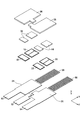
- FIG. 2 is an exploded view of the semiconductor device shown in FIG. 1.
- FIG. 2 is a cross-sectional view of the semiconductor device according to the present embodiment taken along the line AA shown in FIG. It is a top view showing the positional relationship of the semiconductor element and structure in the semiconductor device of a present Example. It is a figure for demonstrating the effect by the semiconductor device of a present Example. It is a figure showing the positional relationship of the semiconductor element and structure in the semiconductor device which is one modification of this invention.
- It is a block diagram of the semiconductor device which is one modification of this invention.
- It is a block diagram of the semiconductor device which is one modification of this invention.
- It is a block diagram of the semiconductor device which is
- FIG. 1 shows a configuration diagram of a semiconductor device 10 according to an embodiment of the present invention.
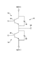
- FIG. 2 shows a circuit configuration diagram of the semiconductor device 10 of the present embodiment.
- FIG. 3 is an exploded view of the semiconductor device 10 shown in FIG.
- FIG. 4 is a cross-sectional view taken along the line AA shown in FIG.
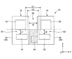
- FIG. 5 is a plan view showing the positional relationship between the semiconductor element and the structure in the semiconductor device 10 of this embodiment.
- FIG. 5 shows a state before the sealing resin is filled.
- the semiconductor device 10 of this embodiment is a power semiconductor module that is mounted on, for example, a hybrid vehicle or an electric vehicle, and is used in a motor control device such as an inverter that performs power conversion.
- the semiconductor device 10 has a mold structure in which upper and lower arms are integrated, and has a double-sided cooling structure in which cooling is performed on both the upper surface and the lower surface.
- the semiconductor device 10 includes an upper arm power unit 12 constituting an upper arm connected to the high potential side power source V + and a lower arm power unit 14 constituting a lower arm connected to the low potential side power source V ⁇ .
- the upper arm power unit 12 has two semiconductor elements 16 and 18 of different types.
- the lower arm power unit 14 has two different semiconductor elements 20 and 22.
- Each of the semiconductor elements 16 to 22 is composed of a semiconductor chip formed in a thin rectangular shape.
- Each of the semiconductor elements 16 and 20 is a power semiconductor switching element such as an insulated gate bipolar transistor (IGBT) that performs a switching operation at the time of power conversion, and the semiconductor elements 18 and 22 are respectively semiconductor elements 16 and 22.
- 20 is a free-wheeling diode that is required to recirculate the current when 20 is cut off.
- the semiconductor elements 16 and 20 are referred to as semiconductor switching elements 16 and 20
- the semiconductor elements 18 and 22 are referred to as diodes 18 and 22, respectively.
- the diode 18 is connected in parallel to the semiconductor switching element 16, and the diode 22 is connected in parallel to the semiconductor switching element 20.
- the semiconductor switching element 16 and the semiconductor switching element 20 are connected in series between the high potential side power source V + and the low potential side power source V ⁇ , and the diode 18 and the diode 22 are connected to the high potential side power source V + and the low potential side power source V +. It is connected in series with the potential side power source V ⁇ .
- the upper arm power unit 12 has one semiconductor switching element 16 and one diode 18 as the two semiconductor elements 16 and 18.
- the lower arm power unit 14 has one semiconductor switching element 20 and one diode 22 as the two semiconductor elements 20 and 22.
- the semiconductor switching elements 16 and 20 each have a collector electrode, an emitter electrode, and a gate electrode.
- the collector electrode is formed on one surface of the semiconductor chip, and the emitter electrode and the gate electrode are formed on the other surface of the semiconductor chip.
- the cathode electrode is formed on one surface of the semiconductor chip, and the anode electrode is formed on the other surface of the semiconductor chip.
- the upper arm power unit 12 has lead frames 24 and 26 provided on both sides of the semiconductor switching element 16 and the diode 18.
- Each of the lead frames 24 and 26 is a flat metal plate and faces each other.
- the semiconductor switching element 16 and the diode 18 of the upper arm power unit 12 are placed on lead frames 24 and 26 (specifically, die pads thereof) and are sandwiched between the two lead frames 24 and 26. It is arranged like this.
- the die pads of the lead frames 24 and 26 have an area larger than the size (area) of each semiconductor element 16 and 18 as a semiconductor chip.
- the semiconductor switching element 16 and the diode 18 are mounted side by side on the lead frames 24 and 26 with a predetermined gap S1 therebetween in the first direction X.
- the one surface of the semiconductor switching element 16 and the one surface of the diode 18 face the lead frame 24. Further, the other surface of the semiconductor switching element 16 and the other surface of the diode 18 face the lead frame 26.
- the lead frames 24 and 26 are conductors made of a metal such as copper, nickel, or aluminum. The lead frames 24 and 26 may have their surfaces plated with silver or gold.
- the bonding material 28 is, for example, solder made of tin or the like, and has conductivity.
- the collector electrode of the semiconductor switching element 16 and the cathode electrode of the diode 18 are electrically connected to the lead frame 24.
- the lead frame 24 is referred to as a collector-side lead frame 24.
- the other surface of the semiconductor switching element 16 and the other surface of the diode 18 are bonded and fixed to the lead frame 26 via a bonding material 30, a conductor block 32, and a bonding material 34.
- the bonding materials 30 and 34 are solders made of, for example, tin, and have conductivity.
- the conductive block 32 is a conductor made of a metal such as copper, and has a thickness in the stacking direction (thickness direction) Z.
- the emitter electrode of the semiconductor switching element 16 and the anode electrode of the diode 18 are electrically connected to the lead frame 26.
- the lead frame 26 is referred to as an emitter-side lead frame 26.
- the lower arm power unit 14 has lead frames 36 and 38 provided on both sides of the semiconductor switching element 20 and the diode 22.
- the lead frames 36 and 38 are metal plates formed in a planar shape, and face each other.
- the semiconductor switching element 20 and the diode 22 of the lower arm power unit 14 are mounted on lead frames 36 and 38 (specifically, die pads thereof) and are sandwiched between the two lead frames 36 and 38. Yes.
- the die pad portions of the lead frames 36 and 38 have an area larger than the size (area) of each semiconductor element 20 and 22 as a semiconductor chip.
- the semiconductor switching element 20 and the diode 22 are mounted side by side on the lead frames 36 and 38 with a predetermined gap S2 therebetween in the first direction X.
- the size of the predetermined gap S1 in the upper arm power unit 12 (length s1 in the direction in which the semiconductor elements 16 and 18 are arranged) and the size of the predetermined gap S2 in the lower arm power unit 14 (semiconductor elements 20, The lengths s2) in the direction in which 22 are arranged are substantially the same.
- the one surface of the semiconductor switching element 20 and the one surface of the diode 22 face the lead frame 36.
- the other surface of the semiconductor switching element 20 and the other surface of the diode 22 face the lead frame 38.
- the lead frames 36 and 38 are conductors made of metal such as copper, nickel, and aluminum.
- the lead frames 36 and 38 may have their surfaces plated with silver or gold, or may be formed of the same type of metal as the lead frames 24 and 26. Alternatively, the lead frames 24 and 26 may be integrally formed and then cut.
- the bonding material 40 is a solder made of, for example, tin and has conductivity.
- the collector electrode of the semiconductor switching element 20 and the cathode electrode of the diode 22 are electrically connected to the lead frame 36.
- the lead frame 36 is referred to as a collector-side lead frame 36.
- the other surface of the semiconductor switching element 20 and the other surface of the diode 22 are bonded and fixed to the lead frame 38 via a bonding material 42, a conductor block 44, and a bonding material 46.
- the bonding materials 42 and 46 are solders made of, for example, tin and have conductivity.
- the conductive block 44 is a conductor made of a metal such as copper, and has a thickness in the stacking direction (thickness direction) Z.
- the emitter electrode of the semiconductor switching element 20 and the anode electrode of the diode 22 are electrically connected to the lead frame 38.
- the lead frame 38 is referred to as an emitter-side lead frame 38.
- the upper arm power unit 12 and the lower arm power unit 14 include a collector-side lead frame 24 of the upper arm power unit 12 and a collector-side lead frame 36 of the lower arm power unit 14 in the second direction Y through a gap S 3.
- the emitter-side lead frame 26 of the upper arm power unit 12 and the emitter-side lead frame 38 of the lower arm power unit 14 are formed to face each other in the second direction Y with a gap S3 therebetween.
- the upper surface of the collector-side lead frame 24 of the upper arm power unit 12 and the upper surface of the collector-side lead frame 36 of the lower arm power unit 14 are at the same height, and the emitter-side lead frame 26 of the upper arm power unit 12
- the lower surface and the lower surface of the emitter-side lead frame 38 of the lower arm power unit 14 are at the same height position.
- the collector-side lead frame 24 of the upper arm power unit 12 is provided with a high-potential side connection terminal 50 connected to the high-potential side power supply V +, and the voltage of the high-potential side power supply V + is connected via the high-potential side connection terminal 50. Is applied.
- the emitter-side lead frame 38 of the lower arm power unit 14 is provided with a low-potential side connection terminal 52 connected to the low-potential side power supply V ⁇ , and the low-potential side power supply is connected via the low-potential side connection terminal 52. A voltage of V ⁇ is applied.
- the collector-side lead frame 36 of the lower arm power unit 14 is provided with an output terminal 54 connected to a load or the like.
- the gate electrode of the semiconductor switching element 16 of the upper arm power unit 12 is connected to the control terminal 56 through a signal wire.
- the gate electrode of the semiconductor switching element 20 of the lower arm power unit 14 is connected to the control terminal 58 via a signal wire.
- These signal wires are bonding wires made of, for example, aluminum or copper.
- the control terminals 56 and 58 are provided at the ends of the upper arm power unit 12 and the lower arm power unit 14 opposite to the side on which the high potential side connection terminal 50, the low potential side connection terminal 52, and the output terminal 54 are provided. It has been.
- the control terminals 56 and 58 are connected to an electronic control unit (ECU) mainly composed of a microcomputer. Control signals supplied from the ECU via the control terminals 56 and 58 and signal wires are supplied to the gate electrodes of the semiconductor switching elements 16 and 20, respectively.
- the control terminals 56 and 58 may be smaller in size than the high potential side connection terminal 50, the low potential side connection terminal 52, and the output terminal 54 through which a large current can flow.
- each of the upper arm power unit 12 and the lower arm power unit 14 has a predetermined thickness in the stacking direction Z, and the thicknesses of the arm power units 12 and 14 in the stacking direction Z are substantially the same.
- the upper arm power unit 12 and the lower arm power unit 14 are arranged in parallel in the second direction Y. Specifically, in the upper arm power unit 12, the semiconductor switching element 16 and the diode 18 are arranged on the lead frames 24 and 26 with a predetermined gap S1 in the first direction X, and in the lower arm power unit 14, the semiconductor switching is performed.
- the element 20 and the diode 22 are arranged on the lead frames 36 and 38 with a predetermined gap S2 in the first direction X, the second direction orthogonal to the first direction X and the thickness direction Z is provided. They are arranged in parallel in the direction Y.
- the upper arm power unit 12 and the lower arm power unit 14 are arranged such that the semiconductor switching elements 16 and 20 face each other in the second direction Y and the diodes 18 and 22 face each other in the second direction Y.
- a predetermined gap S3 (the length of the gap S3 in the second direction Y is s3) is formed between them.
- the gap S1 vacated in the first direction X between the semiconductor elements 16 and 18 in the upper arm power unit 12 and the gap S2 vacated in the first direction X between the semiconductor elements 20 and 22 in the lower arm power unit 14 are:
- the power units 12 and 14 face each other in the second direction Y in which the power units 12 and 14 are arranged.
- the emitter-side lead frame 26 of the upper arm power unit 12 and the collector-side lead frame 36 of the lower arm power unit 14 are connected via a joint portion 60.
- the joint portion 60 is provided in a gap S3 (specifically, a part thereof) in the second direction Y between the upper arm power unit 12 and the lower arm power unit 14.
- the joint portion 60 includes an emitter piece 62 connected to the emitter side lead frame 26 of the upper arm power unit 12, a collector piece 64 connected to the collector side lead frame 36 of the lower arm power unit 14, and the emitter piece 62 and the collector piece 64. And a bonding material 66 to be bonded.
- Each of the emitter piece 62 and the collector piece 64 is a conductor made of a metal such as copper, nickel, or aluminum.
- the emitter piece 62 has a cross-sectional structure extending obliquely stepwise from the end of the emitter-side lead frame 26 of the upper arm power unit 12 toward the end of the collector-side lead frame 36 of the lower arm power unit 14.
- the collector piece 64 has a cross-sectional structure that extends horizontally from the end of the collector-side lead frame 36 of the lower arm power unit 14 toward the end of the collector-side lead frame 24 of the upper arm power unit 12.
- the emitter piece 62 or the collector piece 64 may be formed integrally with the emitter side lead frame 26 or the collector side lead frame 36.
- the bonding material 66 is, for example, solder made of tin or the like, and has conductivity.
- the semiconductor device 10 has a mold structure in which the upper arm power unit 12 and the lower arm power unit 14 arranged in parallel in the second direction Y are integrally resin-sealed.
- the semiconductor device 10 includes a resin portion 70 that integrally seals the upper arm power unit 12 and the lower arm power unit 14 with resin.
- the resin portion 70 is made of, for example, epoxy resin, and performs the above-described resin sealing by being poured into a mold containing the upper arm power unit 12 and the lower arm power unit 14 in a melted state.
- the melted resin portion 70 is poured into the mold on the side where the control terminals 56 and 58 of the two power units 12 and 14 are provided (that is, the control terminals 56 and 58 and the gate electrodes of the semiconductor switching elements 16 and 20).
- the resin sealing by the resin portion 70 includes a part for each of the high potential side connection terminal 50, the low potential side connection terminal 52, the output terminal 54, and the control terminals 56 and 58. Done. Therefore, the high potential side connection terminal 50, the low potential side connection terminal 52, the output terminal 54, and a part of each of the control terminals 56 and 58 are respectively on the main body side (side surrounded by the resin portion 70) of the semiconductor device 10. It protrudes from and is exposed to the outside.
- the resin sealing by the resin portion 70 is performed so that the surfaces of the lead frames 24, 26, 36, and 38 opposite to the bonding surfaces with the semiconductor elements 16 to 22 are exposed to the outside. Therefore, the surfaces of the lead frames 24, 26, 36, and 38 opposite to the bonding surfaces with the semiconductor elements 16 to 22 are exposed to the outside. Heat sinks are attached adjacent to the surfaces of the lead frames 24, 26, 36, and 38 that are opposite to the bonding surfaces with the semiconductor elements 16 to 22, respectively. For this reason, the upper arm power unit 12 and the lower arm power unit 14 are cooled on both the upper and lower surfaces.
- FIG. 6 is a diagram for explaining the effect of the semiconductor device 10 of this embodiment.
- FIG. 6A shows a flow of the resin when the semiconductor device 10 of this embodiment is molded.
- FIG. 6B shows a flow of the resin during molding of the comparative semiconductor device 80 compared with the semiconductor device 10 of the present embodiment.
- the upper arm power unit 12 and the lower arm power unit 14 each have a predetermined thickness in the stacking direction Z, and the semiconductor elements 16 and 18 are located between the two lead frames 24 and 26.
- the semiconductor elements 20 and 22 are sandwiched between the two lead frames 36 and 38.
- the upper arm power unit 12 and the lower arm power unit 14 are configured such that the semiconductor switching element 16 and the diode 18 are arranged with a predetermined gap S1 in the first direction X and the semiconductor switching element 20 and the diode 22 are the first. In a state in which the predetermined gap S2 is arranged in the direction X with the predetermined gap S2 therebetween, the two are arranged in parallel while leaving the predetermined gap S3 in the second direction Y.
- the resin part 70 is molded by melting the main body side of the semiconductor device 10 in the mold and then dissolving it in the mold from the side where the control terminals 56 and 58 of the power units 12 and 14 are provided. By injecting the resin.
- the resin flow in the mold includes the resin flow M flowing through the gap S3 between the upper arm power unit 12 and the lower arm power unit 14, and the outside of the upper arm power unit 12 (that is, , There is a resin flow N that flows outside the lower arm power unit 14 (that is, the gap between the lower arm power unit 14 and the inner wall of the mold).
- a part of the resin based on the flow M and a part of the resin based on the flow N are provided with the high potential side connection terminal 50, the low potential side connection terminal 52, or the output terminal 54 of the power units 12 and 14.
- the other part reaches the mold at the end of the formed side, but the other part flows through the gaps S1 and S2 between the semiconductor switching elements 16 and 20 and the diodes 18 and 22 of the power units 12 and 14, respectively.
- a part of the resin based on the flow M and a part of the resin based on the flow N are the gaps S1 and S2 (regions surrounded by a broken line in FIG. 6B). As a result, there is a high possibility that resin voids and resin peeling will occur.
- the joint portion 60 that connects the power units 12 and 14 is provided in the gap S3 between the upper arm power unit 12 and the lower arm power unit 14.
- the joint 60 is integrally sealed with resin together with the upper arm power unit 12 and the lower arm power unit 14.
- the joint portion 60 serves as a connection portion that connects the emitter-side lead frame 26 of the upper arm power unit 12 and the collector-side lead frame 36 of the lower arm power unit 14, and further, at the time of manufacturing the semiconductor device 10.
- the semiconductor device 10 As a structure formed on the flow path through which the resin flows between the power units 12 and 14 (specifically, the region where the semiconductor elements 16 and 18 and the semiconductor elements 20 and 22 are separated), the semiconductor device 10 or the gold
- the resin that has flowed into the gap S ⁇ b> 3 from the resin inlet of the mold has a role of inhibiting the flow of the resin to the side where the high potential side connection terminal 50, the low potential side connection terminal 52, or the output terminal 54 is provided.
- the joint portion 60 has its end portion (specifically, control terminals 56 and 58 into which resin filled as the resin portion 70 flows during manufacture or molding).
- the side opposite to the resin inlet side than the position corresponding to the end of the semiconductor element 20 on the resin inlet side opposite to the resin inlet side that is, downstream in the resin flow direction).
- the joint portion 60 is provided with control terminals 56 and 58 through which an end portion (specifically, resin filled as the resin portion 70 flows during manufacture or molding).
- the position range corresponding to the gap S1 between the semiconductor elements 16 and 18 and the gap S2 between the semiconductor elements 20 and 22 in the gap S3 between the two power units 12 and 14 (the end portion on the resin inlet side) (FIG. 7). It is more preferable that they are arranged so as to fall within a region indicated by diagonal lines in FIG. Further, in this case, the joint portion 60 is more preferable as its end portion is located at a more downstream position (on the diodes 18 and 22 side) within the position range.
- the joint portion 60 When the joint portion 60 is arranged as described above, a part of the resin flowing into the gap S3 from the resin inlet of the semiconductor device 10 or the mold is blocked by the end of the joint portion 60 on the resin inlet side. Therefore, it is difficult for the resin to flow through the gap S3 toward the side where the high potential side connection terminal 50, the low potential side connection terminal 52, or the output terminal 54 is provided, while the semiconductor elements 16 and 18 are not connected. It becomes easy to flow into the gap S1 and the gap S2 between the semiconductor elements 20 and 22.
- the joint portion 60 connects the power units 12 and 14 in the gap S3 between the upper arm power unit 12 and the lower arm power unit 14.
- the emitter-side lead frame 26 of the upper arm power unit 12 and the collector-side lead frame 36 of the lower arm power unit 14 are connected in the gap S3.
- the joint portion 60 includes the lower surface of the emitter-side lead frame 26 of the upper arm power unit 12 (the lower surface of the emitter-side lead frame 38 of the lower arm power unit 14 is the same) and the collector of the lower arm power unit 14 in the gap S3. It is arranged so as to include a position range corresponding to a region between the upper surface of the side lead frame 36 (note that the upper surface of the collector side lead frame 24 of the upper arm power unit 12 is the same).
- the leads of the power units 12 and 14 This easily flows into the space between the upper surfaces of the frames 24 and 36 and the lower surfaces of the lead frames 26 and 38.
- the flow rate at which the resin flowing through the gap S3 flows into the gaps S1 and S2 is relatively large as compared with the structure of the comparative semiconductor device 80 described above.
- the resin flows into the gaps S1 and S2, and then passes through the gaps S1 and S2 in the second direction Y of the power units 12 and 14 (gap with the inner wall of the mold; FIG. 6A is surrounded by a broken line.
- the time to reach (region) is relatively short.
- the diode 18 located on the side far from the resin inlet into which the resin filled during manufacture flows is The semiconductor switching element 16 located on the side close to the resin inlet is disposed so as to protrude from the end on the gap S3 side so as to protrude toward the gap S3.
- the diode 22 located on the side far from the resin inlet into which the resin filled during manufacture flows is closer to the resin inlet.
- the semiconductor switching element 20 is positioned so as to protrude from the end on the gap S3 side so as to protrude to the gap S3 side.
- the diodes 18 and 22 located on the side far from the resin inlet of each power unit 12 and 14 are both connected to the semiconductor switching elements 16 and 20 located on the side near the resin inlet.
- the diodes 18 and 22 are arranged so as to protrude toward each other in the second direction Y in which they are separated from each other.
- both the diodes 18 and 22 have a structure that prevents the resin flowing in from the resin inflow port from flowing further downstream in the first direction X in the gap S3 on the flow path between the two power units 12 and 14. Functions as a body.
- the first separation distance L1 in the second direction Y between the semiconductor switching element 16 of the upper arm power unit 12 and the semiconductor switching element 20 of the lower arm power unit 14, the diode 18 of the upper arm power unit 12 and the lower arm power unit. 14 diodes 22 and the second separation distance L2 in the second direction Y are different from each other. Specifically, the second separation distance L2 between the diodes 18 and 22 located on the side far from the resin inlet is compared with the first separation distance L1 between the semiconductor switching parts 16 and 20 located on the side closer to the resin inlet. Small.
- the diode 18 positioned on the downstream side in the direction in which the resin flows during resin injection is arranged closer to the gap S3 side than the semiconductor switching element 16 positioned on the upstream side.
- the end of the diode 18 on the second direction Y side (more specifically, on the gap S3 side in the second direction Y) is connected to the second direction Y side of the semiconductor switching element 16 (more Specifically, it is located closer to the gap S3 than the end of the gap S3 in the second direction Y.
- the diode 22 positioned on the downstream side in the direction in which the resin flows during resin injection is arranged closer to the gap S3 side than the semiconductor switching element 20 positioned on the upstream side.
- the end of the diode 22 on the second direction Y side (more specifically, on the gap S3 side in the second direction Y) is connected to the second direction Y side of the semiconductor switching element 20 (more Specifically, it is located closer to the gap S3 than the end of the gap S3 in the second direction Y.
- the width of the flow path through which the resin injected from the resin inlet of the semiconductor device 10 or the mold flows is the upstream side (specifically, the second direction toward the semiconductor switching elements 16 and 20).
- Y which is wide on the downstream side (specifically, on the side facing the diodes 18 and 22 in the second direction Y)
- the resin injected from the resin inlet is After passing through the semiconductor switching elements 16, 20 in the process of flowing between the power units 12, 14 (that is, the gap S 3), a part of the resin becomes the end portion (on the first direction X side) of the diodes 18, 22 ( The upper end in FIG.
- the distance between the power units 12 and 14 is smaller than that of the structure in which the diodes 18 and 22 are not blocked by the end portion (upper end in FIG. 5) on the first direction X side. While the resin flowing into the gap S3 does not easily flow through the gap S3 to the side where the high potential side connection terminal 50, the low potential side connection terminal 52, or the output terminal 54 is provided, the gap between the semiconductor elements 16 and 18 can be reduced. Since the flow rate of the resin flowing into the gaps S1 and S2 becomes relatively large, and the resin flows into the gaps S1 and S2, the flow rate of the resin flows into the gaps S1 and S2. The time until it reaches the outside in the second direction Y of the power units 12, 14 through the gaps S1, S2 (gap with the inner wall of the mold; the area surrounded by the broken line in FIG. 6A) is relatively short. Become.
- the semiconductor device 10 when the semiconductor device 10 is manufactured, the melted resin is poured into the mold from approximately the vicinity of the center where the control terminals 56 and 58 of the power units 12 and 14 are provided.
- a joining position where a part of the resin based on the flow M flowing through the gap S3 joins with the resin based on the flow N after a part of the resin based on the flow M flows into the gaps S1 and S2 is a position within the gaps S1 and S2. Instead, it is possible to set the positions of the power units 12, 14 outside the gaps S1, S2 outside the second direction Y.
- the gap S1 between the two semiconductor elements 16 and 18 of the upper arm power unit 12 and the two semiconductor elements 20 and 22 of the lower arm power unit 14 at the time of molding with resin It is possible to make it difficult for the resin to merge in the gap S2 between the two. For this reason, it is possible to suppress generation
- the lead frames 24, 26, 36, and 38 are the “metal plate” described in the claims, and the semiconductor elements 16 to 22 are the “semiconductor elements” described in the claims.
- the gaps S1 and S2 are the “predetermined gap” described in the claims, the second direction Y is the “predetermined direction” described in the claims, and the upper arm power unit 12 and the lower arm power unit 14 are patented.
- the semiconductor switching elements 16 and 20 are in the “near semiconductor element” in the claims, and the diodes 18 and 22 are in the “distant semiconductor element” in the claims.
- the joint portion 60 and the diodes 18 and 22 are included in the “structure” described in the claims, and the lead frames 26 and 38 are included in the “lead” described in the claims.
- the lead frames 24 and 36 are described in the Claims.
- the first separation distance L1 is described in the Claims.
- the second separation distance L2 corresponds to the “first separation distance” and the “second separation distance” described in the claims.
- the joint portion 60 that connects the upper arm power unit 12 and the lower arm power unit 14 is connected to the lower arm power unit 14 from the end of the emitter-side lead frame 26 of the upper arm power unit 12 as shown in FIG. Is formed so as to extend obliquely stepwise toward the end side of the collector-side lead frame 36, but as shown in FIG. 8, the upper arm has a larger thickness in the stacking direction Y in the gap S3.
- the joint portion 100 that connects the power unit 12 and the lower arm power unit 14 may be formed.
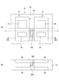
- 8A is a diagram showing the positional relationship between the semiconductor element and the structure in the semiconductor device of this modification
- FIG. 8B is FIG. 8A of the semiconductor device of this modification. III-III sectional views shown in FIG.
- the joint portion 100 includes an emitter piece 102 connected to the emitter-side lead frame 26 of the upper arm power unit 12, a collector piece 104 connected to the collector-side lead frame 36 of the lower arm power unit 14, and copper, for example.
- a conductive block 106 made of metal and having a thickness in the stacking direction (thickness direction) Z; a bonding material 108 for bonding the emitter piece 102 and the conductive block 106; And a bonding material 110 for bonding the collector piece 104.
- the thickness in the stacking direction Z as a structure that blocks the resin can be secured in the gap S3 on the flow path between both the power units 12 and 14, so It becomes easy to perform damming, and the inflow of resin from the gap S3 to the gaps S1 and S2 can be promoted.
- the emitter-side lead frame 26 of the upper arm power unit 12 and the collector-side lead frame 36 of the lower arm power unit 14 are used as a structure that blocks the resin in the gap S3 between the power units 12 and 14.
- the joint portion 60 to be connected is used, the present invention is not limited to this.
- the structure is a low potential connected to the emitter side lead frame 38 of the lower arm power unit 14 or the emitter side lead frame 38.
- the side connection terminal 52 may be used.
- the emitter piece 120 connected to the emitter-side lead frame 38 and the low-potential-side connection terminal 52 may be joined by a joining material 122.
- FIG. 9A is a diagram showing the positional relationship between the semiconductor element and the structure in the semiconductor device of this modification
- FIG. 9B is FIG. 9A of the semiconductor device of this modification. IV-IV sectional views shown in FIG.
- the semiconductor switching elements 16 and 20 are disposed on the resin inlet side on the lead frames 24, 26, 36, and 38 of the power units 12 and 14, and the diodes 18 and 22 are disposed on the opposite side.
- Each of the diodes 18 and 22 may be disposed on the resin inlet side, and the semiconductor switching elements 16 and 20 may be disposed on the opposite side.
- the semiconductor switching elements 16 and 20 located on the side far from the resin inlet of each power unit 12 and 14 are both connected to the diodes 18 and 22 located on the side closer to the resin inlet.
- the two semiconductor switching elements 16 and 20 are disposed so as to protrude toward the side approaching each other. That is, the separation distance between the semiconductor switching devices 16 and 20 located on the side far from the resin inlet is made smaller than the separation distance between the diodes 18 and 22 located on the side closer to the resin inlet.
- the semiconductor switching element 16 is disposed closer to the gap S3 side than the diode 18, and on the lead frames 36 and 38, the semiconductor switching element 20 is closer to the gap 22 than the diode 22. Arranged near the S3 side.
- the joint 60 connecting the power units 12 and 14 has an end on the resin inlet side.
- the semiconductor element 16 is located in the gap S3 so as to be located downstream in the resin flow direction from the position corresponding to the downstream end of the semiconductor switching elements 16 and 20 located upstream in the gap S3.
- 18 and a gap located within the position range corresponding to the gap S2 between the semiconductor elements 20 and 22, and (2) a diode located on the far side from the resin inlet of each of the power units 12 and 14 18 and 22 are connected to the semiconductor switching elements 16 and 20 located on the side close to the resin inflow port.
- the both diodes 18, 22 are assumed to be arranged so as to protrude on the side closer to each other, as long as it (1) and any one or more of (2) is satisfied.
- the upper arm power unit 12 has the two semiconductor elements 16 and 18 and the lower arm power unit 14 has the two semiconductor elements 20 and 22, but the power units 12 and 14 Each may have three or more semiconductor elements.
- each power unit 12, 14 may have three semiconductor elements 200, 202, 204. These semiconductor elements 200, 202 and 204 are arranged side by side with a gap in the first direction X on the power units 12 and 14. These three semiconductor elements 200, 202, and 204 may all be of different types, but may be composed of two same types and two different types and one different type. For example, it may be composed of two semiconductor switching elements and one diode, or conversely, may be composed of one semiconductor switching element and two diodes.
- the semiconductor element 204 located on the side far from the resin inlet into which the resin filled during manufacture flows is the resin inlet.
- the semiconductor element 202 located on the side farther from the resin inlet is arranged so as to protrude from the end on the gap S3 side of the semiconductor switching element 200 located on the side closer to the resin inlet to the gap S3 side. It should be.
- the separation distance L13 between the semiconductor elements 204 located on the farthest side from the resin inlet of the power units 12 and 14 is smaller than the separation distance L12 between the semiconductor elements 202 located at a medium distance from the resin inlet.
- the separation distance L12 is made smaller than the separation distance L11 between the semiconductor elements 200 located on the side closest to the resin inflow port, and the second direction of the semiconductor elements 200, 202, and 204.
- the diodes 18 and 22 located on the side far from the resin inlet of each power unit 12 and 14 are both connected to the semiconductor switching elements 16 and 20 located on the side closer to the resin inlet.
- both the diodes 18 and 22 are projected so as to approach each other, but only one of the diodes 18 and 22 is disposed as shown in FIG.
- the semiconductor switching elements 16 and 20 may be arranged so as to protrude toward the other diodes 22 and 18 in the second direction Y in which the power units 12 and 14 are separated from each other.
- the resin is injected into the mold for forming the resin portion 70 by using the second power unit 12, 14 on the side where the control terminals 56, 58 are provided. This is performed from approximately the center in the direction Y toward the first direction X, but the first direction from the end side in the second direction Y of the two power units 12 and 14 on the side where the control terminals 56 and 58 are provided. It may be performed toward X.
- 60 and the diodes 18 and 22 located farther from the resin inlet but the present invention is not limited to this, and the joint portion 60 and the diodes 18 and 22 or the joint portion Instead of 60 and the diodes 18 and 22, as shown in FIG. 12, a pin 300 provided in a mold that is not integrally resin-sealed together with the power units 12 and 14 may be used.
- 12A is a view showing the positional relationship between the semiconductor element and the structure in the semiconductor device of the present modification
- FIG. 12B is FIG. 12A of the semiconductor device of the present modification. VV sectional views shown in FIG.
- the pin 300 is provided integrally with the mold, and when the semiconductor device 10 is manufactured, the end of the resin inlet side of the semiconductor switching elements 16 and 20 located upstream in the gap S3. More preferably, in the gap S3, the gap S1 between the semiconductor elements 16 and 18 and the gap S2 between the semiconductor elements 20 and 22 are located in the gap S3 so as to be located downstream of the position corresponding to the downstream end. It arrange
- the pin 300 has a position range corresponding to a region between the lower surface of the emitter-side lead frames 26 and 38 of the power units 12 and 14 and the upper surface of the collector-side lead frames 24 and 36 in the gap S3 (FIG. 12B ) Are arranged so as to include at least a part of the region indicated by hatching. In this case, the pin 300 is more preferably arranged so as to include the entire position range.
- the joint portion 60 disposed in the gap S3 is used as the structure for blocking the resin between the power units 12 and 14, but the present invention is not limited to this.
- Such a structure that hinders the flow of the resin may be disposed on the resin flow path between the two power units 12, 14, for example, on the lead frames 24, 26, 36, 38 of the power units 12, 14.
- the semiconductor elements 16 to 22 may be provided separately.
- the semiconductor device 10 has the two power units 12 and 14 arranged in parallel in the second direction Y. However, 3 arranged in parallel in the second direction Y. It is good also as what has two or more power units.
- the semiconductor device 10 is sandwiched between the two lead frames 24 and 26 facing each other or between the two lead frames 36 and 38 facing each other.
- the present invention may be applied to a single-sided cooling structure in which cooling is performed only on one side.
Landscapes
- Encapsulation Of And Coatings For Semiconductor Or Solid State Devices (AREA)
- Inverter Devices (AREA)
- Structures Or Materials For Encapsulating Or Coating Semiconductor Devices Or Solid State Devices (AREA)
- Lead Frames For Integrated Circuits (AREA)
Abstract
Description
12 上アームパワーユニット
14 下アームパワーユニット
16,20 半導体スイッチング素子(半導体素子)
18,22 ダイオード(半導体素子)
24,26,36,38 リードフレーム
50 高電位側接続端子
52 低電位側接続端子
54 出力端子
56,58 制御端子
60 継手部
70 樹脂部
Claims (17)
- 金属板上に複数の半導体素子が所定の隙間を空けて載置されるパワーユニットを複数組、所定方向に並列に配置し、該複数組の前記パワーユニットを一体的に樹脂封止した半導体装置であって、
前記所定方向に互いに隣接して配置される2つの前記パワーユニット間における、製造時に充填される樹脂が流通する流路上の、前記所定の隙間を介して載置される2つの前記半導体素子のうち前記樹脂の流入口に近い側に位置する近方半導体素子の該流入口側とは反対側の端部に対応する所定位置よりも前記樹脂の流通方向下流側に、前記樹脂の流通方向下流側への流通を妨げる構造体を配置したことを特徴とする半導体装置。 - 前記構造体の前記流入口側の端部は、前記所定方向に互いに隣接して配置される2つの前記パワーユニット間の、前記半導体素子同士が離間する領域において、前記所定位置よりも前記樹脂の流通方向下流側に位置することを特徴とする請求項1記載の半導体装置。
- 金属板上に複数の半導体素子が所定の隙間を空けて載置されるパワーユニットを複数組、所定方向に並列に配置し、該複数組の前記パワーユニットを一体的に樹脂封止した半導体装置であって、
製造時に充填される樹脂が流入する流入口側の端部が、前記所定方向に互いに隣接して配置される2つの前記パワーユニット間における前記樹脂が流通する流路上の、前記所定の隙間に対応する位置範囲内に収まるように構造体を配置したことを特徴とする半導体装置。 - 前記構造体は、また、前記流路上の、前記パワーユニットの、前記半導体素子の上面側に設けられる前記金属板としての上面側リードフレームの下面と前記半導体素子の下面側に設けられる前記金属板としての下面側リードフレームの上面との間に対応する位置範囲の少なくとも一部を含むように配置されることを特徴とする請求項1乃至3の何れか一項記載の半導体装置。
- 前記構造体は、前記パワーユニットと共に一体的に樹脂封止されることを特徴とする請求項1乃至4の何れか一項記載の半導体装置。
- 前記構造体は、前記所定方向に互いに隣接して配置される2つの前記パワーユニット同士を繋ぐ継手部であることを特徴とする請求項5記載の半導体装置。
- 各パワーユニットはそれぞれ、前記半導体素子の両面側それぞれに設けられる前記金属板としてのリードフレームを有し、
前記構造体は、前記所定方向に互いに隣接して配置される2つの前記パワーユニットのうち、一方の前記パワーユニットの前記半導体素子の上面側に設けられる上面側リードフレームと、他方の前記パワーユニットの前記半導体素子の下面側に設けられる下面側リードフレームと、を繋ぐ継手部であることを特徴とする請求項6記載の半導体装置。 - 前記構造体は、各パワーユニットの複数の半導体素子のうち、製造時に充填される樹脂が流入する流入口に近い側に位置する近方半導体素子の前記所定方向の端部から前記所定方向に飛び出るように突出して配置された、前記流入口から遠い側に位置する遠方半導体素子であることを特徴とする請求項5記載の半導体装置。
- 前記所定方向に互いに隣接して配置される2つの前記パワーユニットの前記遠方半導体素子は共に、前記所定方向で両遠方半導体素子が互いに近づく側に突出して配置されることを特徴とする請求項8記載の半導体装置。
- 前記所定方向に互いに隣接して配置される2つの前記パワーユニット間における、前記近方半導体素子同士の第1離間距離と、前記遠方半導体素子同士の第2離間距離と、を互いに異ならせたことを特徴とする請求項8又は9記載の半導体装置。
- 前記第2離間距離を前記第1離間距離よりも小さくしたことを特徴とする請求項10記載の半導体装置。
- 各パワーユニットにおける、前記第1の半導体素子の前記所定方向における中心位置と、前記第2の半導体素子の前記所定方向における中心位置と、を互いに前記所定方向にオフセットさせたことを特徴とする請求項8乃至11の何れか一項記載の半導体装置。
- 前記パワーユニットは、複数の前記半導体素子として、一つのパワートランジスタと一つの還流ダイオードとを有することを特徴とする請求項1乃至12の何れか一項記載の半導体装置。
- 金属板上に複数の半導体素子が所定の隙間を空けて載置されるパワーユニットを複数組、所定方向に並列に配置し、該複数組の前記パワーユニットを一体的に樹脂封止した半導体装置の製造方法であって、
前記所定方向に互いに隣接して配置される2つの前記パワーユニット間における、製造時に充填される樹脂が流通する流路上の、前記所定の隙間を介して載置される2つの前記半導体素子のうち前記樹脂の流入口に近い側に位置する近方半導体素子の該流入口側とは反対側の端部に対応する所定位置よりも前記樹脂の流通方向下流側に、前記樹脂の流通方向下流側への流通を妨げる構造体を配置したうえで、前記樹脂を充填することを特徴とする半導体装置の製造方法。 - 金属板上に複数の半導体素子が所定の隙間を空けて載置されるパワーユニットを複数組、所定方向に並列に配置し、該複数組の前記パワーユニットを一体的に樹脂封止した半導体装置の製造方法であって、
製造時に充填される樹脂が流入する流入口側の端部が、前記所定方向に互いに隣接して配置される2つの前記パワーユニット間における前記樹脂が流通する流路上の、前記所定の隙間に対応する位置範囲内に収まるように構造体を配置したうえで、前記樹脂を充填することを特徴とする半導体装置の製造方法。 - 前記構造体を、また、前記流路上の、前記パワーユニットの、前記半導体素子の上面側に設けられる前記金属板としての上面側リードフレームの下面と前記半導体素子の下面側に設けられる前記金属板としての下面側リードフレームの上面との間に対応する位置範囲の少なくとも一部を含むように配置したうえで、前記樹脂を充填することを特徴とする請求項14又は15記載の半導体装置の製造方法。
- 前記構造体が金型に設けられたピンであることを特徴とする請求項16記載の半導体装置の製造方法。
Priority Applications (4)
| Application Number | Priority Date | Filing Date | Title |
|---|---|---|---|
| US14/383,316 US9312211B2 (en) | 2012-03-07 | 2013-02-28 | Semiconductor device and manufacturing method thereof |
| EP13757297.0A EP2824696B1 (en) | 2012-03-07 | 2013-02-28 | Semiconductor device and method of manufacture thereof |
| CN201380012899.2A CN104160493B (zh) | 2012-03-07 | 2013-02-28 | 半导体装置及其制造方法 |
| JP2014503803A JP5845336B2 (ja) | 2012-03-07 | 2013-02-28 | 半導体装置及びその製造方法 |
Applications Claiming Priority (2)
| Application Number | Priority Date | Filing Date | Title |
|---|---|---|---|
| JP2012-050992 | 2012-03-07 | ||
| JP2012050992 | 2012-03-07 |
Publications (1)
| Publication Number | Publication Date |
|---|---|
| WO2013133134A1 true WO2013133134A1 (ja) | 2013-09-12 |
Family
ID=49116615
Family Applications (1)
| Application Number | Title | Priority Date | Filing Date |
|---|---|---|---|
| PCT/JP2013/055523 Ceased WO2013133134A1 (ja) | 2012-03-07 | 2013-02-28 | 半導体装置及びその製造方法 |
Country Status (5)
| Country | Link |
|---|---|
| US (1) | US9312211B2 (ja) |
| EP (1) | EP2824696B1 (ja) |
| JP (1) | JP5845336B2 (ja) |
| CN (1) | CN104160493B (ja) |
| WO (1) | WO2013133134A1 (ja) |
Cited By (6)
| Publication number | Priority date | Publication date | Assignee | Title |
|---|---|---|---|---|
| JP2015162598A (ja) * | 2014-02-27 | 2015-09-07 | トヨタ自動車株式会社 | 半導体装置の製造方法および製造装置 |
| CN105575937A (zh) * | 2014-11-04 | 2016-05-11 | 丰田自动车株式会社 | 半导体装置和用于半导体装置的制造方法 |
| EP3021355A1 (en) * | 2014-10-30 | 2016-05-18 | Toyota Jidosha Kabushiki Kaisha | Method of joining a semiconductor element to a joined member using a tin-containing solder material with copper particles dispersed therein and corresponding semiconductor device |
| EP3021357A1 (en) * | 2014-10-30 | 2016-05-18 | Toyota Jidosha Kabushiki Kaisha | Method of joining a semiconductor element to a joined member by reacting a tin-containing solder material with a copper layer on the joined member and corresponding semiconductor device |
| WO2016076015A1 (ja) * | 2014-11-13 | 2016-05-19 | 株式会社日立製作所 | パワー半導体モジュール |
| JP2016134591A (ja) * | 2015-01-22 | 2016-07-25 | 株式会社デンソー | 半導体装置の製造方法 |
Families Citing this family (13)
| Publication number | Priority date | Publication date | Assignee | Title |
|---|---|---|---|---|
| JP6221542B2 (ja) * | 2013-09-16 | 2017-11-01 | 株式会社デンソー | 半導体装置 |
| JP2017103434A (ja) * | 2015-12-04 | 2017-06-08 | トヨタ自動車株式会社 | 半導体装置 |
| JP6686691B2 (ja) * | 2016-05-16 | 2020-04-22 | 株式会社デンソー | 電子装置 |
| JP6822000B2 (ja) * | 2016-08-05 | 2021-01-27 | 株式会社デンソー | 半導体装置 |
| JP6772768B2 (ja) * | 2016-11-09 | 2020-10-21 | 株式会社デンソー | 半導体装置 |
| JP2018101664A (ja) * | 2016-12-19 | 2018-06-28 | トヨタ自動車株式会社 | 半導体装置の製造方法 |
| JP6586970B2 (ja) * | 2017-03-09 | 2019-10-09 | トヨタ自動車株式会社 | 半導体装置 |
| JP6768569B2 (ja) * | 2017-03-21 | 2020-10-14 | ルネサスエレクトロニクス株式会社 | 半導体装置の製造方法および半導体装置 |
| JP2020120037A (ja) * | 2019-01-25 | 2020-08-06 | トヨタ自動車株式会社 | 半導体モジュールの製造方法 |
| EP3739624A1 (en) * | 2019-05-13 | 2020-11-18 | Infineon Technologies Austria AG | Semiconductor arrangement with a compressible contact element encapsulated between two carriers and corresponding manufacturing method |
| EP4092731A1 (en) * | 2021-05-20 | 2022-11-23 | Infineon Technologies Austria AG | Method of forming a semiconductor package with connection lug |
| US12125772B2 (en) | 2021-05-20 | 2024-10-22 | Infineon Technologies Austria Ag | Method of forming a semiconductor package with connection lug |
| US11728250B2 (en) | 2021-05-20 | 2023-08-15 | Infineon Technologies Austria Ag | Semiconductor package with connection lug |
Citations (4)
| Publication number | Priority date | Publication date | Assignee | Title |
|---|---|---|---|---|
| JP2005123495A (ja) * | 2003-10-20 | 2005-05-12 | Mitsubishi Electric Corp | 半導体装置の製造方法および半導体装置 |
| JP2006120970A (ja) * | 2004-10-25 | 2006-05-11 | Toyota Motor Corp | 半導体モジュールとその製造方法 |
| JP2010258315A (ja) | 2009-04-28 | 2010-11-11 | Hitachi Automotive Systems Ltd | パワーモジュール及び電力変換装置 |
| WO2011162241A1 (ja) * | 2010-06-21 | 2011-12-29 | 日立オートモティブシステムズ株式会社 | 電力変換装置 |
Family Cites Families (13)
| Publication number | Priority date | Publication date | Assignee | Title |
|---|---|---|---|---|
| EP2244289B1 (en) | 2000-04-19 | 2014-03-26 | Denso Corporation | Coolant cooled type semiconductor device |
| JP4192396B2 (ja) | 2000-04-19 | 2008-12-10 | 株式会社デンソー | 半導体スイッチングモジュ−ル及びそれを用いた半導体装置 |
| JP4403665B2 (ja) | 2001-03-14 | 2010-01-27 | 三菱電機株式会社 | 半導体装置 |
| EP1513195A4 (en) * | 2002-06-13 | 2009-06-24 | Panasonic Corp | SEMICONDUCTOR COMPONENT AND METHOD FOR THE PRODUCTION THEREOF |
| DE602004014504D1 (de) | 2004-10-18 | 2008-07-31 | Thermagen | Selbstkühlende Flasche |
| JP4374312B2 (ja) * | 2004-12-21 | 2009-12-02 | 三菱電機株式会社 | 車載回転電機における半導体スイッチング素子とヒートシンクとの組み立て方法および車載回転電機 |
| JP4805636B2 (ja) | 2005-08-30 | 2011-11-02 | 株式会社東芝 | 電力用半導体素子及び半導体電力変換装置 |
| DE102006012781B4 (de) * | 2006-03-17 | 2016-06-16 | Infineon Technologies Ag | Multichip-Modul mit verbessertem Systemträger und Verfahren zu seiner Herstellung |
| JP4403166B2 (ja) | 2006-11-06 | 2010-01-20 | 株式会社日立製作所 | パワーモジュールおよび電力変換装置 |
| JP4864990B2 (ja) | 2009-01-29 | 2012-02-01 | 三菱電機株式会社 | 半導体装置 |
| JP5422466B2 (ja) | 2010-04-01 | 2014-02-19 | 日立オートモティブシステムズ株式会社 | 電力変換装置 |
| JP5557585B2 (ja) | 2010-04-26 | 2014-07-23 | 日立オートモティブシステムズ株式会社 | パワーモジュール |
| JP5947537B2 (ja) | 2011-04-19 | 2016-07-06 | トヨタ自動車株式会社 | 半導体装置及びその製造方法 |
-
2013
- 2013-02-28 WO PCT/JP2013/055523 patent/WO2013133134A1/ja not_active Ceased
- 2013-02-28 US US14/383,316 patent/US9312211B2/en active Active
- 2013-02-28 EP EP13757297.0A patent/EP2824696B1/en active Active
- 2013-02-28 CN CN201380012899.2A patent/CN104160493B/zh active Active
- 2013-02-28 JP JP2014503803A patent/JP5845336B2/ja active Active
Patent Citations (4)
| Publication number | Priority date | Publication date | Assignee | Title |
|---|---|---|---|---|
| JP2005123495A (ja) * | 2003-10-20 | 2005-05-12 | Mitsubishi Electric Corp | 半導体装置の製造方法および半導体装置 |
| JP2006120970A (ja) * | 2004-10-25 | 2006-05-11 | Toyota Motor Corp | 半導体モジュールとその製造方法 |
| JP2010258315A (ja) | 2009-04-28 | 2010-11-11 | Hitachi Automotive Systems Ltd | パワーモジュール及び電力変換装置 |
| WO2011162241A1 (ja) * | 2010-06-21 | 2011-12-29 | 日立オートモティブシステムズ株式会社 | 電力変換装置 |
Non-Patent Citations (1)
| Title |
|---|
| See also references of EP2824696A4 |
Cited By (11)
| Publication number | Priority date | Publication date | Assignee | Title |
|---|---|---|---|---|
| JP2015162598A (ja) * | 2014-02-27 | 2015-09-07 | トヨタ自動車株式会社 | 半導体装置の製造方法および製造装置 |
| EP3021355A1 (en) * | 2014-10-30 | 2016-05-18 | Toyota Jidosha Kabushiki Kaisha | Method of joining a semiconductor element to a joined member using a tin-containing solder material with copper particles dispersed therein and corresponding semiconductor device |
| EP3021357A1 (en) * | 2014-10-30 | 2016-05-18 | Toyota Jidosha Kabushiki Kaisha | Method of joining a semiconductor element to a joined member by reacting a tin-containing solder material with a copper layer on the joined member and corresponding semiconductor device |
| CN105575937A (zh) * | 2014-11-04 | 2016-05-11 | 丰田自动车株式会社 | 半导体装置和用于半导体装置的制造方法 |
| EP3018711A1 (en) * | 2014-11-04 | 2016-05-11 | Toyota Jidosha Kabushiki Kaisha | Semiconductor device and manufacturing method for the semiconductor device |
| RU2612944C1 (ru) * | 2014-11-04 | 2017-03-14 | Тойота Дзидося Кабусики Кайся | Полупроводниковое устройство и способ изготовления полупроводникового устройства |
| KR101759398B1 (ko) * | 2014-11-04 | 2017-07-31 | 도요타지도샤가부시키가이샤 | 반도체 장치와 그 제조 방법 |
| US9847311B2 (en) | 2014-11-04 | 2017-12-19 | Toyota Jidosha Kabushiki Kaisha | Semiconductor device and manufacturing method for the semiconductor device |
| AU2017248560B2 (en) * | 2014-11-04 | 2018-11-08 | Toyota Jidosha Kabushiki Kaisha | Semiconductor device and manufacturing method for the semiconductor device |
| WO2016076015A1 (ja) * | 2014-11-13 | 2016-05-19 | 株式会社日立製作所 | パワー半導体モジュール |
| JP2016134591A (ja) * | 2015-01-22 | 2016-07-25 | 株式会社デンソー | 半導体装置の製造方法 |
Also Published As
| Publication number | Publication date |
|---|---|
| US20150028466A1 (en) | 2015-01-29 |
| JP5845336B2 (ja) | 2016-01-20 |
| CN104160493B (zh) | 2017-03-22 |
| EP2824696A8 (en) | 2015-06-24 |
| EP2824696B1 (en) | 2021-05-05 |
| CN104160493A (zh) | 2014-11-19 |
| JPWO2013133134A1 (ja) | 2015-07-30 |
| EP2824696A4 (en) | 2015-05-20 |
| US9312211B2 (en) | 2016-04-12 |
| EP2824696A1 (en) | 2015-01-14 |
Similar Documents
| Publication | Publication Date | Title |
|---|---|---|
| JP5845336B2 (ja) | 半導体装置及びその製造方法 | |
| CN103688352B (zh) | 半导体器件及半导体器件的制造方法 | |
| US8497572B2 (en) | Semiconductor module and method of manufacturing the same | |
| KR101585306B1 (ko) | 반도체 장치 및 그 제조 방법 | |
| US9240371B2 (en) | Semiconductor module, semiconductor device having semiconductor module, and method of manufacturing semiconductor module | |
| US9831160B2 (en) | Semiconductor device | |
| CN114175234B (zh) | 半导体装置及电子装置 | |
| KR101928681B1 (ko) | 전력용 반도체 장치 및 그 제조 방법 | |
| JP7100569B2 (ja) | 半導体モジュール、電力変換装置および半導体モジュールの製造方法 | |
| TW201911427A (zh) | 半導體模組之製造方法及半導體模組 | |
| CN111587528B (zh) | 功率半导体装置 | |
| CN100565850C (zh) | 半导体器件 | |
| CN104009013A (zh) | 具有单独的管芯间互连的多管芯封装 | |
| US10818573B2 (en) | Power semiconductor module with heat dissipation plate | |
| JP7046742B2 (ja) | パワーモジュール | |
| US12476161B2 (en) | Semiconductor package with lead frame | |
| CN105359262A (zh) | 半导体装置的制造方法、半导体装置 | |
| JP7845824B2 (ja) | 半導体装置 | |
| JP6001472B2 (ja) | 半導体装置の製造方法 | |
| CN116646326B (zh) | 智能功率模块和具有其的电子设备 | |
| US20220301966A1 (en) | Semiconductor device | |
| JP2019029410A (ja) | 半導体モジュール | |
| CN110911375A (zh) | 半导体装置 | |
| CN202977407U (zh) | 半导体模块 | |
| JP4258411B2 (ja) | 半導体装置 |
Legal Events
| Date | Code | Title | Description |
|---|---|---|---|
| 121 | Ep: the epo has been informed by wipo that ep was designated in this application |
Ref document number: 13757297 Country of ref document: EP Kind code of ref document: A1 |
|
| NENP | Non-entry into the national phase |
Ref country code: DE |
|
| WWE | Wipo information: entry into national phase |
Ref document number: 2013757297 Country of ref document: EP |
|
| ENP | Entry into the national phase |
Ref document number: 2014503803 Country of ref document: JP Kind code of ref document: A |
|
| WWE | Wipo information: entry into national phase |
Ref document number: 14383316 Country of ref document: US |