WO2013146290A1 - 保護素子 - Google Patents
保護素子 Download PDFInfo
- Publication number
- WO2013146290A1 WO2013146290A1 PCT/JP2013/057162 JP2013057162W WO2013146290A1 WO 2013146290 A1 WO2013146290 A1 WO 2013146290A1 JP 2013057162 W JP2013057162 W JP 2013057162W WO 2013146290 A1 WO2013146290 A1 WO 2013146290A1
- Authority
- WO
- WIPO (PCT)
- Prior art keywords
- cover member
- heating element
- flux
- projecting portion
- insulating substrate
- Prior art date
- Legal status (The legal status is an assumption and is not a legal conclusion. Google has not performed a legal analysis and makes no representation as to the accuracy of the status listed.)
- Ceased
Links
Images


Classifications
-
- H—ELECTRICITY
- H01—ELECTRIC ELEMENTS
- H01H—ELECTRIC SWITCHES; RELAYS; SELECTORS; EMERGENCY PROTECTIVE DEVICES
- H01H37/00—Thermally-actuated switches
- H01H37/74—Switches in which only the opening movement or only the closing movement of a contact is effected by heating or cooling
- H01H37/76—Contact member actuated by melting of fusible material, actuated due to burning of combustible material or due to explosion of explosive material
- H01H37/767—Normally open
-
- H—ELECTRICITY
- H01—ELECTRIC ELEMENTS
- H01H—ELECTRIC SWITCHES; RELAYS; SELECTORS; EMERGENCY PROTECTIVE DEVICES
- H01H85/00—Protective devices in which the current flows through a part of fusible material and this current is interrupted by displacement of the fusible material when this current becomes excessive
- H01H85/0013—Means for preventing damage, e.g. by ambient influences to the fuse
- H01H85/0021—Means for preventing damage, e.g. by ambient influences to the fuse water or dustproof devices
- H01H85/003—Means for preventing damage, e.g. by ambient influences to the fuse water or dustproof devices casings for the fusible element
-
- H—ELECTRICITY
- H01—ELECTRIC ELEMENTS
- H01H—ELECTRIC SWITCHES; RELAYS; SELECTORS; EMERGENCY PROTECTIVE DEVICES
- H01H85/00—Protective devices in which the current flows through a part of fusible material and this current is interrupted by displacement of the fusible material when this current becomes excessive
- H01H85/0039—Means for influencing the rupture process of the fusible element
- H01H85/0047—Heating means
-
- H—ELECTRICITY
- H01—ELECTRIC ELEMENTS
- H01M—PROCESSES OR MEANS, e.g. BATTERIES, FOR THE DIRECT CONVERSION OF CHEMICAL ENERGY INTO ELECTRICAL ENERGY
- H01M50/00—Constructional details or processes of manufacture of the non-active parts of electrochemical cells other than fuel cells, e.g. hybrid cells
- H01M50/50—Current conducting connections for cells or batteries
- H01M50/572—Means for preventing undesired use or discharge
- H01M50/574—Devices or arrangements for the interruption of current
- H01M50/581—Devices or arrangements for the interruption of current in response to temperature
-
- H—ELECTRICITY
- H01—ELECTRIC ELEMENTS
- H01H—ELECTRIC SWITCHES; RELAYS; SELECTORS; EMERGENCY PROTECTIVE DEVICES
- H01H85/00—Protective devices in which the current flows through a part of fusible material and this current is interrupted by displacement of the fusible material when this current becomes excessive
- H01H85/0013—Means for preventing damage, e.g. by ambient influences to the fuse
- H01H85/0021—Means for preventing damage, e.g. by ambient influences to the fuse water or dustproof devices
- H01H2085/0034—Means for preventing damage, e.g. by ambient influences to the fuse water or dustproof devices with molded casings
-
- H—ELECTRICITY
- H01—ELECTRIC ELEMENTS
- H01M—PROCESSES OR MEANS, e.g. BATTERIES, FOR THE DIRECT CONVERSION OF CHEMICAL ENERGY INTO ELECTRICAL ENERGY
- H01M10/00—Secondary cells; Manufacture thereof
- H01M10/05—Accumulators with non-aqueous electrolyte
- H01M10/052—Li-accumulators
- H01M10/0525—Rocking-chair batteries, i.e. batteries with lithium insertion or intercalation in both electrodes; Lithium-ion batteries
-
- H—ELECTRICITY
- H01—ELECTRIC ELEMENTS
- H01M—PROCESSES OR MEANS, e.g. BATTERIES, FOR THE DIRECT CONVERSION OF CHEMICAL ENERGY INTO ELECTRICAL ENERGY
- H01M2200/00—Safety devices for primary or secondary batteries
- H01M2200/10—Temperature sensitive devices
- H01M2200/103—Fuse
-
- Y—GENERAL TAGGING OF NEW TECHNOLOGICAL DEVELOPMENTS; GENERAL TAGGING OF CROSS-SECTIONAL TECHNOLOGIES SPANNING OVER SEVERAL SECTIONS OF THE IPC; TECHNICAL SUBJECTS COVERED BY FORMER USPC CROSS-REFERENCE ART COLLECTIONS [XRACs] AND DIGESTS
- Y02—TECHNOLOGIES OR APPLICATIONS FOR MITIGATION OR ADAPTATION AGAINST CLIMATE CHANGE
- Y02E—REDUCTION OF GREENHOUSE GAS [GHG] EMISSIONS, RELATED TO ENERGY GENERATION, TRANSMISSION OR DISTRIBUTION
- Y02E60/00—Enabling technologies; Technologies with a potential or indirect contribution to GHG emissions mitigation
- Y02E60/10—Energy storage using batteries
Definitions
- the present invention relates to a protection element that protects a circuit connected on a current path by fusing the current path.
- a battery pack In particular, in lithium ion secondary batteries with high weight energy density, in order to ensure the safety of users and electronic devices, a battery pack generally includes a number of protection circuits such as overcharge protection and overdischarge protection. It has a function of shutting off the output of the battery pack in a predetermined case.
- the battery pack is overcharge protected or overdischarge protected by turning the output on and off using the FET switch built in the battery pack.
- the FET switch is short-circuited for some reason, a lightning surge, etc. is applied, a momentary large current flows, or the output voltage drops abnormally due to the life of the battery cell.
- the battery pack and the electronic device must be protected from accidents such as ignition even when the is output. Accordingly, in order to safely shut off the output of the battery cell in any possible abnormal state, a protection element composed of a fuse element having a function of cutting off a current path by an external signal is used.
- the protection element As a protection element of such a protection circuit for a lithium ion secondary battery or the like, as described in Patent Document 1, the protection element has a heating element, and the heating element causes a soluble conductor on the current path. In general, a structure for fusing is used.
- a flux is applied to the surface of a soluble conductor (fuse) made of a low melting point metal for the purpose of preventing oxidation, promoting melting, and improving fusing characteristics.
- a cover member is provided so as to cover the substrate constituting the protection element in order to ensure the quality of the protection element.
- the cover member has a cylindrical projecting shape on the inner surface of the cover member so as to surround the central portion on the soluble conductor in order to hold the applied flux and make the flux amount on the soluble conductor uniform. Has a part.
- Patent Document 1 describes a protection element in which a void is discharged by providing a cutout in a cylindrical protrusion.
- a void is discharged by providing a cutout in a cylindrical protrusion.
- the flux flows out from the notch provided in the cylindrical protrusion, resulting in a variation in the amount of flux applied on the soluble conductor.
- an object of the present invention is to realize a protective element in which even if voids are generated in the flux applied on the soluble conductor, the amount of the flux is made uniform and the fusing characteristics are improved.
- a protection element includes an insulating substrate, a heating element stacked on the insulating substrate, and an insulating member stacked on the insulating substrate so as to cover at least the heating element.
- the first and second electrodes stacked on the insulating substrate on which the insulating members are stacked, and the insulating member so as to overlap the heating element, and on the current path between the first and second electrodes And a heating element internal electrode electrically connected to the heating element, and a laminate between the heating element internal electrode and the first and second electrodes, and a current between the first electrode and the second electrode by heating.
- the cover member has an annular protrusion formed on the inner surface of the cover member so as to face the heating element so as to be in contact with the flux, and the wall surface of the annular protrusion covers the inside of the protrusion.
- a communication hole communicating with the inner surface side of the member is opened.
- the cover member has an annular protrusion formed so as to be in contact with the flux so as to face the heating element, and the inner surface side of the cover member from the inside of the protrusion on the wall surface of the annular protrusion Since the communication hole communicating with is opened, the void generated in the flux can be discharged from the communication hole. By discharging the voids, the flux applied on the soluble conductor becomes uniform, the heat distribution of the soluble conductor becomes uniform, and the variation in fusing characteristics is reduced.
- FIG. 1A is a cross-sectional view taken along line A-A ′ of a cover member constituting a protective element to which the present invention is applied.
- FIG. 1B is a bottom view of the cover member.
- FIG. 2A is a plan view in a state where a cover member is removed in order to show a configuration of a protection element to which the present invention is applied.
- 2B is a cross-sectional view taken along the line B-B ′ showing the structure of the protection element in a state where a cover member is attached to the protection element of FIG. 2A.
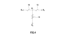
- It is a figure which shows the circuit structural example of the protection element to which this invention was applied.
- FIG. 5A is a cross-sectional view of the A-A ′ portion of a cover member constituting a conventional protection element.
- FIG. 5B is a bottom view of a cover member that constitutes a conventional protection element, and is a conceptual diagram showing a state in which a flux and a void generated in the flux are discharged.
- (C) is sectional drawing of a protection element.
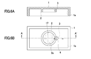
- FIG. 6A is a cross-sectional view of the A-A ′ portion of the cover member constituting the protective element to which the present invention is applied.
- FIG. 6B is a bottom view of the protection element, conceptually showing a void generated in the flux and a state in which the void is discharged from the communication hole.
- FIG. 7A is a cross-sectional view showing an example of a communication hole opened in the wall surface of the protruding portion of the cover member.
- FIG. 7B is a cross-sectional view illustrating another example of the communication hole opened in the wall surface of the protruding portion of the cover member.
- FIG. 8A is a cross-sectional view of a cover member showing one of the modifications of the embodiment of the protection element of the present invention.
- FIG. 8B is a bottom view.
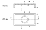
- FIG. 9A is a cross-sectional view of a cover member showing one of modifications of the embodiment of the protection element of the present invention.
- FIG. 9B is a bottom view. It is a figure which shows the protrusion part supported by the columnar support member which concerns on the modification of FIG.
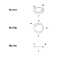
- FIG. 10A is a perspective view of a protrusion.
- FIG. 10B is a plan view.
- FIG. 10C is a front view.
- the cover member 1 has a protruding portion 2 having a tip disposed on the inner surface 1a of the cover member 1 at a position facing the position of the heating element 14.
- the protruding portion 2 has a cylindrical shape with the inner surface 1a of the cover member 1 as a bottom surface and an open end.
- the cylindrical projecting portion 2 is disposed at a position facing the rectangular heating element 14 via the fusible conductor 13 when the cover member 1 is attached to the main body of the protection element 10.
- the height of the cylindrical projection 2 is determined so that the tip of the cylindrical projection 2 is in contact with the surface of the flux 17 applied to the surface of the soluble conductor 13.
- the inner surface 2 a of the cylindrical protrusion 2 is a space where the flux 17 is attracted and filled with the flux 17 by the surface tension of the flux 17 in contact with the tip.
- the wall surface of the inner surface 2a may be smooth or may be textured and rough.
- a communication hole 3 is provided that communicates the inner surface 2 a of the projecting portion 2 and the inner surface 1 a side of the cover member 1.
- the cover member 1 is used for protecting the inside of the protection element 10 and is formed of an insulating material.
- an insulating material having a predetermined heat resistance such as glass epoxy or ceramics can be used.
- the cover member 1 is generally formed by integral molding including the projecting portion 2 using an injection molding technique, but the projecting portion 2 is suitable for the inner surface 1a of the cover member 1 as another component. You may comprise by adhesion
- the main body of the protection element 10 includes an insulating substrate 11, a heating element 14 laminated on the insulating substrate 11 and covered with an insulating member 15, and electrodes 12 formed on both ends of the insulating substrate 11. 12, a heating element internal electrode 16 laminated on the insulating member 15 so as to overlap the heating element 14, both ends connected to the electrodes 12, 12, and a central portion connected to the heating element internal electrode 16 And a conductor 13.
- a flux 17 is applied on the soluble conductor 13.
- the protection element 10 according to the present invention is entirely configured by covering the cover member 1 of FIG. 1 on the insulating substrate 11 of the main body of the protection element 10. When the cover member 1 is placed on the insulating substrate 11, the cylindrical protrusion 2 comes into contact with the surface of the flux 17, and the inside of the cylindrical protrusion 2 is filled with the flux 17 due to the surface tension of the flux 17.
- the rectangular insulating substrate 11 is formed of an insulating member such as alumina, glass ceramics, mullite, zirconia, and the like.
- an insulating member such as alumina, glass ceramics, mullite, zirconia, and the like.
- the material used for printed wiring boards such as a glass epoxy board
- the heating element 14 is a conductive member that has a relatively high resistance value and generates heat when energized, and is made of, for example, W, Mo, Ru, or the like. These alloys, compositions, or compound powders are mixed with a resin binder or the like to form a paste on the insulating substrate 11 by patterning using a screen printing technique and firing.
- the insulating member 15 is disposed so as to cover the heating element 14, and the heating element internal electrode 16 is disposed so as to face the heating element 14 through the insulating member 15.
- One end of the heating element internal electrode 16 is connected to the heating element electrode 18. Further, one end of the heating element 14 is connected to the other heating element electrode 18.
- the fusible conductor 13 may be a conductive material that melts and blows with a predetermined electric power and heat.
- An alloy or the like can be used.
- the flux 17 has a low viscosity when the protection element 10 is manufactured, and spreads and distributes almost uniformly when applied on the soluble conductor 13. The solvent evaporates over time and the viscosity increases.
- the protection element 10 described above is used in a circuit in a battery pack of a lithium ion secondary battery.
- the protective element 10 is used by being incorporated in a battery pack 20 having a battery stack 25 composed of battery cells 21 to 24 of a total of four lithium ion secondary batteries.
- the battery pack 20 includes a battery stack 25, a charge / discharge control circuit 30 that controls charge / discharge of the battery stack 25, a protection element 10 to which the present invention that protects the battery stack 25 and the charge / discharge control circuit 30 is applied, A detection circuit 26 that detects the voltages of the battery cells 21 to 24 and a current control element 27 that controls the operation of the protection element 10 according to the detection result of the detection circuit 26 are provided.
- the battery stack 25 includes battery cells 21 to 24 that need to be controlled to protect overcharge and overdischarge states.
- the battery stack 25 is detachable via the positive electrode terminal 20a and the negative electrode terminal 20b of the battery pack 20. Are connected to the charging device 35, and a charging voltage from the charging device 35 is applied thereto.
- the electronic device can be operated by connecting the battery pack 20 charged by the charging device 35 to the positive terminal 20a and the negative terminal 20b to the electronic device that is operated by the battery.
- the charge / discharge control circuit 30 includes two current control elements 31 and 32 connected in series to a current path flowing from the battery stack 25 to the charging device 35, and a control unit 33 that controls operations of these current control elements 31 and 32. Is provided.
- the current control elements 31 and 32 are configured by, for example, field effect transistors (hereinafter referred to as FETs), and control the gate voltage by the control unit 33 to control conduction and interruption of the current path of the battery stack 25. .
- FETs field effect transistors
- the control unit 33 operates by receiving power supply from the charging device 35, and according to the detection result by the detection circuit 26, when the battery stack 25 is overdischarged or overcharged, current control is performed so as to cut off the current path. The operation of the elements 31 and 32 is controlled.
- Protective element 10 is connected, for example, on a charge / discharge current path between battery stack 25 and charge / discharge control circuit 30, and its operation is controlled by current control element 27.
- the detection circuit 26 is connected to the battery cells 21 to 24, detects the voltage values of the battery cells 21 to 24, and supplies the voltage values to the control unit 33 of the charge / discharge control circuit 30.
- the detection circuit 26 outputs a control signal for controlling the current control element 27 when any one of the battery cells 21 to 24 becomes an overcharge voltage or an overdischarge voltage.
- the current control element 27 operates the protection element 10 when the voltage value of the battery cells 21 to 24 exceeds a predetermined overdischarge or overcharge state by the detection signal output from the detection circuit 26, Control is performed so that the charging / discharging current path of the battery stack 25 is cut off regardless of the switching operation of the current control elements 31 and 32.
- the protection element 10 to which the present invention is applied has a circuit configuration as shown in FIG.
- the protective element 10 generates heat by melting the soluble conductor 13 by energizing the soluble conductor 13 connected in series via the heating element internal electrode 16 and the connection point of the soluble conductor 13 to generate heat.
- This is a circuit configuration comprising the body 14.
- the fusible conductor 13 is connected in series on the charge / discharge current path, and the heating element 14 is connected to the current control element 27.
- the two electrodes 12 and 12 of the protection element 10 one is connected to A1, and the other is connected to A2.
- the heating element internal electrode 16 and the heating element electrode 18 connected thereto are connected to P1, and the other heating element electrode 18 is connected to P2.
- the protective element 10 having such a circuit configuration can surely melt the soluble conductor 13 on the current path by the heat generation of the heating element 14 while realizing a low profile.
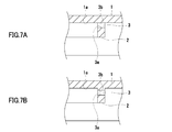
- the cover member 1 of the conventional protection element has a protruding portion 42 disposed on the inner surface 1a of the cover member 1 at a position opposite to the position where the heating element 14 is disposed.
- the protruding portion 42 has a cylindrical shape, the bottom surface is constituted by the inner surface 1a of the cover member 1, the inner surface 42a, and the tip is open.
- the area at the tip of the protrusion 42 is set so as to cover approximately 80% of the area of the rectangular heating element 14 facing the protrusion 42.
- a void ( Bubbles) 44 may be generated. If the void 44 remains in the projecting portion 42, the flux 17 is unevenly distributed in the projecting portion 42, and the uniformity of the flux 17 on the soluble conductor 13 is impaired. As a result, the heat generation distribution of the soluble conductor 13 by the heating element 14 becomes non-uniform, which causes variations in the fusing characteristics of the soluble conductor 13.
- the cover member 1 has a notch 43 formed from the tip of the projecting portion 42 toward the inner surface 1 a of the cover member 1 that is the bottom surface of the projecting portion 42.
- the void 44 in the position of the broken line generated in the flux in the protrusion 42 is discharged to the inner surface 1a side of the cover member 1 through the notch 43 by buoyancy.
- the flux 17 flows out onto the soluble conductor 13 through the notch 43.
- the amount of the flux 17 held by the protrusion 42 is reduced, and a difference occurs in the amount of the flux 17 applied on the soluble conductor 13.
- the heat distribution at locations corresponding to the heating elements 14 on the fusible conductor 13 is unevenly distributed, which causes variations in the fusing characteristics of the fusible conductor 13.
- the protruding portion 2 is formed so that the flux 17 contacts the entire periphery of the tip of the protruding portion 2 of the cover member 1 so as to face the heating element 14. Since it is formed, a sufficient amount of flux 17 can be drawn over a large area that can sufficiently cover the surface area of the heating element 14.
- the cylindrical projecting portion 2 has a communication hole 3 that communicates from the inner surface 2 a of the projecting portion 2 to the inner surface 1 a side of the cover member 1.
- the void 4 generated in the step passes through the communication hole 3 according to the buoyancy and is discharged from the protrusion 2 toward the inner surface 1a of the cover member 1. Therefore, only the void 4 is discharged through the communication hole, and the flux 17 remains at a position corresponding to the heating element 14 on the soluble conductor 13 with a uniform amount.
- the communication hole 3 formed in the wall surface of the projecting portion 2 includes a surface 3 a on the tip side of the projecting portion 2 of the communication hole 3, a surface 3 b on the cover member 1 side, It is surrounded by a side surface not shown.
- the surface 3 b on the cover member 1 side is preferably on the same plane as the inner surface 1 a of the cover member 1.
- FIG. 7B when the surface 3b on the cover member 1 side of the communication hole 3 is formed to have a step from the inner surface 1a of the cover member 1, it moves to the inner surface 1a side of the cover member 1 by buoyancy.
- the void 4 becomes difficult to be discharged because the step is a barrier to the void 4 that has been removed. Further, for example, when the thickness of the portion of the inner surface 1a of the cover member 1 corresponding to the bottom surface in the cylindrical projecting portion 46 is set so as to gradually increase from the communication hole 3 with an inclination, the generated voids are formed in the communication hole. It becomes guided toward 3 and becomes easy to discharge
- the shape of the communication hole is not limited to a square shape, but may be an elliptical shape or an arbitrary shape.
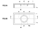
- the number of communication holes 47 opened in the wall surface of the projecting portion 46 is not limited to one, and a plurality of communication holes 47 may be provided, as shown in FIGS. 8A and 8B, an equal distance on the circumference of the projecting portion 46. Alternatively, four openings may be opened. Since the void in the flux 17 in the protrusion 46 moves on the inner surface 46a side of the protrusion 46 by buoyancy, the void in the protrusion 46 is increased by increasing the number of locations where the communication holes 47 are opened. It becomes possible to discharge efficiently.
- the cover member 1 has a cylindrical projecting portion 2 that is open at both ends and has an inner surface 2a, and a surface of the projecting portion 2 on the inner surface 1a side of the cover member 1. And a columnar support portion 48 having one end connected to a part of 2c. In the cover member 1, the other end of the columnar support portion 48 is connected to the inner surface 1 a of the cover member 1.
- the projecting portion 2 is supported by the columnar support portion 48, and the communication hole is formed between the surface 2 c of the projecting portion 2 on the side not contacting the flux 17 and the inner surface 1 a of the cover member 1. 3 is formed in a slit shape.
- the circumferential surface on the side in contact with the flux 17 of the projecting portion 2 can be in contact with the flux 17 all over the soluble conductor 13 without forming the outflow path of the flux 17. It is possible to draw the flux 17 evenly.
- the protrusion 2 and the columnar support 48 connected to the protrusion 2 as shown in FIGS. 9A and 9B can be formed by integral molding using the cover member 1 and an injection molding technique. .
- a projecting member composed of the projecting portion 2 and a columnar support portion 48 connected to the projecting portion 2 is independently integrally molded and separately molded. It can also be formed by connecting to a cover member that does not have a protrusion.
- all of the annular protrusions are cylindrical protrusions.
- it is not limited to the cylindrical shape, and may be an elliptical cylinder, or may be a triangular or other polygonal cylinder.
- Cover member 1a Inner surface of cover member, 2, 42, 44, 46-57 Projection, 2a, 42a-49a Projection, 10 Protection element, 11 Insulating substrate, 12 Electrode, 13 Soluble conductor, 14 heating element, 15 insulating member, 16 heating element internal electrode, 17 flux, 18 heating element electrode, 20 battery pack, 20a positive terminal, 20b negative terminal, 21-24 battery cell, 25 battery stack, 26 detection circuit, 27, 31, 32 Current control element, 30 charge / discharge control circuit, 33 control unit, 35 charging device
Landscapes
- Chemical & Material Sciences (AREA)
- Chemical Kinetics & Catalysis (AREA)
- Electrochemistry (AREA)
- General Chemical & Material Sciences (AREA)
- Engineering & Computer Science (AREA)
- Combustion & Propulsion (AREA)
- Fuses (AREA)
Description
本出願は、日本国において2012年3月26日に出願された日本特許出願番号特願2012-069658を基礎として優先権を主張するものであり、この出願は参照されることにより、本出願に援用される。
ができる。ボイドが排出されることによって、可溶導体上に塗布されたフラックスが均一になって、可溶導体の発熱分布が均一になり、溶断特性のばらつきが低減する。
図1A、図1B、図2A及び図2Bに示すように、カバー部材1は、カバー部材1の内面1aに、発熱体14の位置に対向する位置にその先端が配置された突状部2を有する。突状部2は、カバー部材1の内面1aを底面とし、先端が開口した円筒形状を呈する。円筒状の突状部2は、カバー部材1を保護素子10の本体に被せて取り付けたときに、可溶導体13を介して方形状の発熱体14に対向する位置に配置される。円筒状の突状部2の先端は、可溶導体13の表面に塗布されたフラックス17の表面に接する位置となるように、円筒状の突状部2の高さが決定される。円筒状の突状部2の内面2aは、先端に接したフラックス17の表面張力によって、フラックス17が引き寄せられてフラックス17で満たされるような空間となっている。内面2aの壁面は、滑らかであってもよく、梨地状でざらざらしていてもよい。突状部2の壁面には、突状部2の内面2aとカバー部材1の内面1a側とを連通する連通孔3が開口されている。カバー部材1は、保護素子10の内部の保護用に用いられ、絶縁性の材料により形成される。たとえば、ガラスエポキシ、セラミックス等、所定の耐熱性を有する絶縁材料を用いることができる。カバー部材1は、射出成型技術を用いて、突状部2を含めて一体成型により形成するのが一般的だが、突状部2を別の構成部品として、カバー部材1の内面1aに適切な位置に接着あるいははめ込む等によって構成してもよい。
図3に示すように、上述した保護素子10は、リチウムイオン2次電池のバッテリパック内の回路に用いられる。
以下、本発明に係る保護素子10に用いるカバー部材1の機能について説明するに当たり、従来の保護素子のカバー部材の機能について説明する。
突状部46の壁面に開口される連通孔47は、1個に限られず、複数個あってもよく、図8A及び図8Bに示すように、突状部46の円周上に均等な距離だけ離間させて、4個開口してもよい。突状部46内のフラックス17中のボイドは、浮力によって突状部46の内面46a側を移動するので、連通孔47が開口される箇所を多くすることによって、突状部46内のボイドを効率よく排出することができるようになる。
連通孔の開口した面積を増やすことによって、突状部内のフラックス17中のボイドを、より効率的に排出することができる。図9A及び図9Bに示すように、カバー部材1は、端部がいずれも開口され、内面2aを有する円筒状の突状部2と、突状部2のカバー部材1の内面1a側の面2cの一部に一端が接続された柱状支持部48とを有している。そして、カバー部材1は、柱状支持部48の他端がカバー部材1の内面1aに接続されている。この変形例におけるカバー部材1では、突状部2を柱状支持部48によって支持して、突状部2のフラックス17に接しない側の面2cとカバー部材1の内面1aとの間に連通孔3がスリット状に形成される。突状部2をこのように構成することによって、突状部2の内面2a側に発生したフラックス17のボイド4は、ほぼすべての方向に対して、カバー部材1の内面1aの側へ排出されることができる。
Claims (5)
- 絶縁基板と、
上記絶縁基板に積層された発熱体と、
少なくとも上記発熱体を覆うように、上記絶縁基板に積層された絶縁部材と、
上記絶縁部材が積層された上記絶縁基板に積層された第1及び第2の電極と、
上記発熱体と重畳するように上記絶縁部材の上に積層され、上記第1及び第2の電極の間の電流経路上と該発熱体とに電気的に接続された発熱体内部電極と、
上記発熱体内部電極から上記第1及び第2の電極にわたって積層され、加熱により、該第1の電極と該第2の電極との間の電流経路を溶断する可溶導体と、
上記発熱体と重畳するように、上記低融点金属上に塗布されたフラックスと、
少なくとも上記低融点金属を覆って上記絶縁基板に取り付けられるカバー部材とを備え、
上記カバー部材は、上記発熱体に対向して該カバー部材の内面に、上記フラックスに接するように形成された環状の突状部を有し、
上記環状の突状部の壁面には、該突状部内から上記カバー部材の内面側に連通する連通孔が開口されていることを特徴とする保護素子。 - 上記環状の突状部には、複数個の上記連通孔が開口されていることを特徴とする請求項1記載の保護素子。
- 上記環状の突状部は、円筒形状であり、上記複数個の連通孔は、該円筒形状の周上を均等な距離だけ離間して開口されていることを特徴とする請求項2記載の保護素子。
- 上記連通孔は、上記カバー部材の内面と同一面を有することを特徴とする請求1~3いずれか1項記載の保護素子。
- 上記環状の突状部は、柱状の支持部により上記カバー部材の内面に接続されていることを特徴とする請求項1記載の保護素子。
Priority Applications (5)
| Application Number | Priority Date | Filing Date | Title |
|---|---|---|---|
| US14/386,362 US20150048922A1 (en) | 2012-03-26 | 2013-03-14 | Protection element |
| HK15105018.0A HK1204505A1 (en) | 2012-03-26 | 2013-03-14 | Protection element |
| CN201380017066.5A CN104185888A (zh) | 2012-03-26 | 2013-03-14 | 保护元件 |
| KR1020147029619A KR20140139041A (ko) | 2012-03-26 | 2013-03-14 | 보호 소자 |
| EP13770140.5A EP2851924A4 (en) | 2012-03-26 | 2013-03-14 | ELEMENT OF PROTECTION |
Applications Claiming Priority (2)
| Application Number | Priority Date | Filing Date | Title |
|---|---|---|---|
| JP2012-069658 | 2012-03-26 | ||
| JP2012069658A JP5844669B2 (ja) | 2012-03-26 | 2012-03-26 | 保護素子 |
Publications (1)
| Publication Number | Publication Date |
|---|---|
| WO2013146290A1 true WO2013146290A1 (ja) | 2013-10-03 |
Family
ID=49259553
Family Applications (1)
| Application Number | Title | Priority Date | Filing Date |
|---|---|---|---|
| PCT/JP2013/057162 Ceased WO2013146290A1 (ja) | 2012-03-26 | 2013-03-14 | 保護素子 |
Country Status (8)
| Country | Link |
|---|---|
| US (1) | US20150048922A1 (ja) |
| EP (1) | EP2851924A4 (ja) |
| JP (1) | JP5844669B2 (ja) |
| KR (1) | KR20140139041A (ja) |
| CN (1) | CN104185888A (ja) |
| HK (1) | HK1204505A1 (ja) |
| TW (1) | TWI543224B (ja) |
| WO (1) | WO2013146290A1 (ja) |
Families Citing this family (15)
| Publication number | Priority date | Publication date | Assignee | Title |
|---|---|---|---|---|
| JP5876346B2 (ja) * | 2012-03-26 | 2016-03-02 | デクセリアルズ株式会社 | 保護素子 |
| US9576930B2 (en) * | 2013-11-08 | 2017-02-21 | Taiwan Semiconductor Manufacturing Co., Ltd. | Thermally conductive structure for heat dissipation in semiconductor packages |
| JP6223142B2 (ja) * | 2013-11-20 | 2017-11-01 | デクセリアルズ株式会社 | 短絡素子 |
| JP6314731B2 (ja) * | 2014-08-01 | 2018-04-25 | 株式会社ソシオネクスト | 半導体装置及び半導体装置の製造方法 |
| JP6382028B2 (ja) * | 2014-08-26 | 2018-08-29 | デクセリアルズ株式会社 | 回路基板及び電子部品の実装方法 |
| KR102340112B1 (ko) * | 2015-03-16 | 2021-12-15 | 삼성에스디아이 주식회사 | 단락부재를 갖는 이차 전지 |
| US11024924B2 (en) * | 2016-10-14 | 2021-06-01 | Tiveni Mergeco, Inc. | Methods of welding a bonding connector of a contact plate to a battery cell terminal |
| JP7029784B2 (ja) * | 2017-10-17 | 2022-03-04 | 内橋エステック株式会社 | 保護素子 |
| JP7281274B2 (ja) * | 2018-12-19 | 2023-05-25 | デクセリアルズ株式会社 | 保護素子及びバッテリパック |
| TWI684311B (zh) * | 2019-04-01 | 2020-02-01 | 聚鼎科技股份有限公司 | 保護元件 |
| TWI700719B (zh) * | 2019-12-13 | 2020-08-01 | 聚鼎科技股份有限公司 | 保護元件及其電路保護裝置 |
| TWI801242B (zh) | 2022-05-17 | 2023-05-01 | 功得電子工業股份有限公司 | 具有蓋體的保護元件 |
| JP7397921B1 (ja) * | 2022-07-05 | 2023-12-13 | レノボ・シンガポール・プライベート・リミテッド | 放熱構造、および電子機器 |
| JP2024057541A (ja) * | 2022-10-12 | 2024-04-24 | デクセリアルズ株式会社 | 保護素子及び保護素子の製造方法 |
| TWI860116B (zh) * | 2023-10-05 | 2024-10-21 | 功得電子工業股份有限公司 | 貼片型保險絲及其熔絲件 |
Citations (2)
| Publication number | Priority date | Publication date | Assignee | Title |
|---|---|---|---|---|
| JP2003156036A (ja) * | 2001-11-20 | 2003-05-30 | Nippon Densan Corp | 動圧流体軸受装置 |
| JP2010003665A (ja) | 2008-05-23 | 2010-01-07 | Sony Chemical & Information Device Corp | 保護素子及び二次電池装置 |
Family Cites Families (11)
| Publication number | Priority date | Publication date | Assignee | Title |
|---|---|---|---|---|
| US5712610C1 (en) * | 1994-08-19 | 2002-06-25 | Sony Chemicals Corp | Protective device |
| JP4396787B2 (ja) * | 1998-06-11 | 2010-01-13 | 内橋エステック株式会社 | 薄型温度ヒュ−ズ及び薄型温度ヒュ−ズの製造方法 |
| JP2000306477A (ja) * | 1999-04-16 | 2000-11-02 | Sony Chem Corp | 保護素子 |
| JP2001325869A (ja) * | 2000-05-17 | 2001-11-22 | Sony Chem Corp | 保護素子 |
| JP5301298B2 (ja) * | 2009-01-21 | 2013-09-25 | デクセリアルズ株式会社 | 保護素子 |
| JP5130233B2 (ja) * | 2009-01-21 | 2013-01-30 | デクセリアルズ株式会社 | 保護素子 |
| JP5130232B2 (ja) * | 2009-01-21 | 2013-01-30 | デクセリアルズ株式会社 | 保護素子 |
| US8472158B2 (en) * | 2009-09-04 | 2013-06-25 | Cyntec Co., Ltd. | Protective device |
| US9129769B2 (en) * | 2009-09-04 | 2015-09-08 | Cyntec Co., Ltd. | Protective device |
| US9025295B2 (en) * | 2009-09-04 | 2015-05-05 | Cyntec Co., Ltd. | Protective device and protective module |
| JP6099383B2 (ja) * | 2011-12-19 | 2017-03-22 | デクセリアルズ株式会社 | 保護素子、保護素子の製造方法、及び、保護素子が組み込まれたバッテリモジュール |
-
2012
- 2012-03-26 JP JP2012069658A patent/JP5844669B2/ja not_active Expired - Fee Related
-
2013
- 2013-03-14 KR KR1020147029619A patent/KR20140139041A/ko not_active Withdrawn
- 2013-03-14 WO PCT/JP2013/057162 patent/WO2013146290A1/ja not_active Ceased
- 2013-03-14 CN CN201380017066.5A patent/CN104185888A/zh active Pending
- 2013-03-14 EP EP13770140.5A patent/EP2851924A4/en not_active Withdrawn
- 2013-03-14 HK HK15105018.0A patent/HK1204505A1/xx unknown
- 2013-03-14 US US14/386,362 patent/US20150048922A1/en not_active Abandoned
- 2013-03-20 TW TW102109781A patent/TWI543224B/zh not_active IP Right Cessation
Patent Citations (2)
| Publication number | Priority date | Publication date | Assignee | Title |
|---|---|---|---|---|
| JP2003156036A (ja) * | 2001-11-20 | 2003-05-30 | Nippon Densan Corp | 動圧流体軸受装置 |
| JP2010003665A (ja) | 2008-05-23 | 2010-01-07 | Sony Chemical & Information Device Corp | 保護素子及び二次電池装置 |
Non-Patent Citations (1)
| Title |
|---|
| See also references of EP2851924A4 * |
Also Published As
| Publication number | Publication date |
|---|---|
| JP2013201064A (ja) | 2013-10-03 |
| TWI543224B (zh) | 2016-07-21 |
| EP2851924A4 (en) | 2016-01-27 |
| TW201346965A (zh) | 2013-11-16 |
| KR20140139041A (ko) | 2014-12-04 |
| CN104185888A (zh) | 2014-12-03 |
| JP5844669B2 (ja) | 2016-01-20 |
| HK1204505A1 (en) | 2015-11-20 |
| US20150048922A1 (en) | 2015-02-19 |
| EP2851924A1 (en) | 2015-03-25 |
Similar Documents
| Publication | Publication Date | Title |
|---|---|---|
| JP5844669B2 (ja) | 保護素子 | |
| KR102004018B1 (ko) | 보호 소자 | |
| TWI653653B (zh) | Protective component | |
| JP2012003878A (ja) | 保護素子、及び、保護素子の製造方法 | |
| HK1207740A1 (en) | Protection element | |
| KR20160142303A (ko) | 보호 소자, 보호 회로 및 배터리 회로 | |
| WO2014021157A1 (ja) | 保護素子及びバッテリパック | |
| TWI652712B (zh) | Protective component | |
| TWI680482B (zh) | 保護元件 | |
| KR20160106547A (ko) | 보호 소자 | |
| KR20150121089A (ko) | 보호 소자 및 전자 기기 | |
| JP6542576B2 (ja) | 保護素子、二次電池の保護回路および電池パック | |
| JP2014127270A (ja) | 保護素子 | |
| WO2015107632A1 (ja) | 保護素子 | |
| HK1179405B (en) | Protection element, and method for producing protection element |
Legal Events
| Date | Code | Title | Description |
|---|---|---|---|
| 121 | Ep: the epo has been informed by wipo that ep was designated in this application |
Ref document number: 13770140 Country of ref document: EP Kind code of ref document: A1 |
|
| WWE | Wipo information: entry into national phase |
Ref document number: 14386362 Country of ref document: US |
|
| NENP | Non-entry into the national phase |
Ref country code: DE |
|
| REEP | Request for entry into the european phase |
Ref document number: 2013770140 Country of ref document: EP |
|
| WWE | Wipo information: entry into national phase |
Ref document number: 2013770140 Country of ref document: EP |
|
| ENP | Entry into the national phase |
Ref document number: 20147029619 Country of ref document: KR Kind code of ref document: A |