WO2013153991A1 - 固体撮像装置 - Google Patents
固体撮像装置 Download PDFInfo
- Publication number
- WO2013153991A1 WO2013153991A1 PCT/JP2013/060088 JP2013060088W WO2013153991A1 WO 2013153991 A1 WO2013153991 A1 WO 2013153991A1 JP 2013060088 W JP2013060088 W JP 2013060088W WO 2013153991 A1 WO2013153991 A1 WO 2013153991A1
- Authority
- WO
- WIPO (PCT)
- Prior art keywords
- signal line
- voltage
- pixel
- vertical signal
- noise
- Prior art date
- Legal status (The legal status is an assumption and is not a legal conclusion. Google has not performed a legal analysis and makes no representation as to the accuracy of the status listed.)
- Ceased
Links
Images


Classifications
-
- H—ELECTRICITY
- H10—SEMICONDUCTOR DEVICES; ELECTRIC SOLID-STATE DEVICES NOT OTHERWISE PROVIDED FOR
- H10F—INORGANIC SEMICONDUCTOR DEVICES SENSITIVE TO INFRARED RADIATION, LIGHT, ELECTROMAGNETIC RADIATION OF SHORTER WAVELENGTH OR CORPUSCULAR RADIATION
- H10F39/00—Integrated devices, or assemblies of multiple devices, comprising at least one element covered by group H10F30/00, e.g. radiation detectors comprising photodiode arrays
- H10F39/10—Integrated devices
- H10F39/12—Image sensors
- H10F39/18—Complementary metal-oxide-semiconductor [CMOS] image sensors; Photodiode array image sensors
-
- H—ELECTRICITY
- H04—ELECTRIC COMMUNICATION TECHNIQUE
- H04N—PICTORIAL COMMUNICATION, e.g. TELEVISION
- H04N25/00—Circuitry of solid-state image sensors [SSIS]; Control thereof
- H04N25/40—Extracting pixel data from image sensors by controlling scanning circuits, e.g. by modifying the number of pixels sampled or to be sampled
- H04N25/46—Extracting pixel data from image sensors by controlling scanning circuits, e.g. by modifying the number of pixels sampled or to be sampled by combining or binning pixels
-
- H—ELECTRICITY
- H04—ELECTRIC COMMUNICATION TECHNIQUE
- H04N—PICTORIAL COMMUNICATION, e.g. TELEVISION
- H04N25/00—Circuitry of solid-state image sensors [SSIS]; Control thereof
- H04N25/60—Noise processing, e.g. detecting, correcting, reducing or removing noise
-
- H—ELECTRICITY
- H04—ELECTRIC COMMUNICATION TECHNIQUE
- H04N—PICTORIAL COMMUNICATION, e.g. TELEVISION
- H04N25/00—Circuitry of solid-state image sensors [SSIS]; Control thereof
- H04N25/60—Noise processing, e.g. detecting, correcting, reducing or removing noise
- H04N25/616—Noise processing, e.g. detecting, correcting, reducing or removing noise involving a correlated sampling function, e.g. correlated double sampling [CDS] or triple sampling
-
- H—ELECTRICITY
- H04—ELECTRIC COMMUNICATION TECHNIQUE
- H04N—PICTORIAL COMMUNICATION, e.g. TELEVISION
- H04N25/00—Circuitry of solid-state image sensors [SSIS]; Control thereof
- H04N25/60—Noise processing, e.g. detecting, correcting, reducing or removing noise
- H04N25/67—Noise processing, e.g. detecting, correcting, reducing or removing noise applied to fixed-pattern noise, e.g. non-uniformity of response
- H04N25/671—Noise processing, e.g. detecting, correcting, reducing or removing noise applied to fixed-pattern noise, e.g. non-uniformity of response for non-uniformity detection or correction
- H04N25/677—Noise processing, e.g. detecting, correcting, reducing or removing noise applied to fixed-pattern noise, e.g. non-uniformity of response for non-uniformity detection or correction for reducing the column or line fixed pattern noise
-
- H—ELECTRICITY
- H04—ELECTRIC COMMUNICATION TECHNIQUE
- H04N—PICTORIAL COMMUNICATION, e.g. TELEVISION
- H04N25/00—Circuitry of solid-state image sensors [SSIS]; Control thereof
- H04N25/70—SSIS architectures; Circuits associated therewith
- H04N25/76—Addressed sensors, e.g. MOS or CMOS sensors
- H04N25/78—Readout circuits for addressed sensors, e.g. output amplifiers or A/D converters
-
- H—ELECTRICITY
- H10—SEMICONDUCTOR DEVICES; ELECTRIC SOLID-STATE DEVICES NOT OTHERWISE PROVIDED FOR
- H10F—INORGANIC SEMICONDUCTOR DEVICES SENSITIVE TO INFRARED RADIATION, LIGHT, ELECTROMAGNETIC RADIATION OF SHORTER WAVELENGTH OR CORPUSCULAR RADIATION
- H10F39/00—Integrated devices, or assemblies of multiple devices, comprising at least one element covered by group H10F30/00, e.g. radiation detectors comprising photodiode arrays
- H10F39/80—Constructional details of image sensors
- H10F39/811—Interconnections
Definitions
- the present invention relates to a solid-state imaging device.
- an amplification type solid-state imaging device that converts a signal charge accumulated in a photoelectric conversion element into a signal voltage in a pixel and outputs it to a signal line, such as a CMOS (complementary metal-oxide semiconductor) image sensor, is known.
- CMOS complementary metal-oxide semiconductor
- This solid-state imaging device has a voltage (hereinafter referred to as a noise voltage) generated when resetting a charge-voltage conversion element in a pixel, and a voltage obtained by adding a signal charge generated by photoelectric conversion to the noise voltage (hereinafter referred to as a noise voltage).
- the signal noise sum voltage is output from the charge-voltage conversion element in the pixel, and two capacitive elements that are held separately are provided in all the vertical signal lines.
- the noise voltage and the signal noise sum voltage from all the pixels in the row selected by the vertical shift register are held in the capacitive element, and then provided in the column selected by the horizontal shift register.
- a noise voltage and a signal noise sum voltage are sequentially output from two capacitive elements.
- Patent Document 1 since the solid-state imaging device disclosed in Patent Document 1 includes capacitive elements twice as many as the number of vertical signal lines on the chip of the CMOS image sensor, a peripheral circuit including a capacitive element portion with respect to the pixel array. The area ratio of the part increases.
- the present invention has been made in view of the above-described circumstances, and reduces the number of capacitive elements on a chip while maintaining a signal with high noise resistance, and includes a capacitive element portion with respect to the pixel array portion.
- An object of the present invention is to provide a solid-state imaging device capable of reducing the area ratio of a circuit portion.
- One embodiment of the present invention includes a plurality of unit pixels arranged two-dimensionally, a plurality of transfer lines in which a plurality of pixel groups including one or more unit pixels are connected in common, the transfer lines, and the like.
- a noise voltage generated when the charge-voltage conversion element is reset and a signal noise sum voltage obtained by adding the signal voltage generated by photoelectric conversion to the noise voltage belongs to the pixel group including the unit pixel It is a solid-state imaging device which outputs each to another different transfer line connected to the transfer line via the switch.
- the noise voltage generated by resetting the charge-voltage conversion element of one unit pixel is transferred to another transfer line connected to the transfer line to which the unit pixel is connected via the switch. Output when the switch is turned on.
- the signal noise sum voltage output from one unit pixel is transferred to a transfer line connected to the transfer line to which the unit pixel is connected via another switch and different from the transfer line that outputs the noise voltage. It is output by turning on the other switch.
- the signal voltage can be easily obtained by subtracting the noise voltage output to another transfer line from the signal noise sum voltage output to one transfer line. Only one capacitive element (for example, a capacitive element or a parasitic capacitance of a transfer line) is required. As a result, the noise voltage can be subtracted from the signal noise sum voltage to obtain a signal with high noise resistance, and the number of capacitive elements on the chip can be reduced to include the capacitive element portion with respect to the pixel array portion. The area ratio of the circuit portion can be reduced.
- each of the switches may be provided on a wiring that connects the transfer line and a plurality of other transfer lines arranged at an equal distance from the transfer line.
- each of the switches may be provided so that the noise voltage and the signal noise sum voltage output from each of the unit pixels are respectively output to the plurality of other transfer lines. Good.
- capacitance of the capacitive element holding a noise voltage and a signal noise sum voltage can be increased. This is particularly effective when parasitic capacitance is used as a capacitive element.
- the plurality of unit pixels arranged two-dimensionally are divided into a plurality of groups each including three or more transfer lines, and the control unit selects one of the unit pixels in each group. Select and operate the switch to output and hold the noise voltage to the first other transfer line, and operate the switch to output and hold the signal noise sum voltage to the second other transfer line. The noise voltage and the signal noise sum voltage held in these two transfer lines are read out. Then, by switching the unit pixels to be selected sequentially and repeating the above operation, a signal with high noise resistance can be obtained from all the unit pixels.
- the power supply voltage connected to the unit pixel is enabled to enable the voltage output from the unit pixel and to disable the voltage output from the unit pixel.
- Power supply voltage switching means for switching to a potential, and when the control unit outputs a noise voltage and a signal noise sum voltage from the selected unit pixel, the power supply voltage supplied to the unit pixel is set as an enable potential, and the same
- the power supply voltage switching means is controlled so that the power supply voltage supplied to the other unit pixels in the group is set to a disable potential.
- the present invention while maintaining a signal with high noise resistance, the number of capacitive elements on the chip can be reduced, and the area ratio of the peripheral circuit part including the capacitive element part to the pixel array part can be reduced. It is possible to provide a solid-state imaging device.
- FIG. 1 is a circuit diagram showing a configuration of a solid-state imaging device according to a first embodiment of the present invention. It is a circuit diagram which shows the structure of the pixel with which the solid-state imaging device of FIG. 1 is provided.
- 2 is a timing chart showing the operation of the solid-state imaging device of FIG. 1. It is a circuit diagram which shows the structure of the solid-state imaging device which concerns on the 2nd Embodiment of this invention. 5 is a timing chart showing the operation of the solid-state imaging device of FIG. It is a circuit diagram which shows the structure of the solid-state imaging device which concerns on the 3rd Embodiment of this invention. 7 is a timing chart illustrating an operation of the solid-state imaging device in FIG. 6.
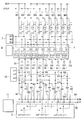
- the solid-state imaging device includes a pixel array 3 including a plurality of pixels P, a vertical shift register 4, a horizontal shift register 5, a timing generator (power supply voltage switching means) 7, and a vertical signal line.
- a selection circuit 10 and a control circuit (control unit) 11 are provided.
- the pixel array 3 includes a plurality of pixels P arranged in a matrix, that is, a predetermined number in the row direction and the column direction, and the pixels P belonging to the same column have common vertical signal lines 81, 82, 83, 84, 85, 86, 87, 88, 89.
- Each vertical signal line 81, 82, 83, 84, 85, 86, 87, 88, 89 is connected to a common horizontal signal line 9A, 9B via horizontal signal line selection switches SA1 to SB9 (described later).
- the current source connection switches Si1 to Si9 (described later) are connected to the constant current sources Ic1 to Ic9.
- the vertical shift register 4 selects one row from the pixel array 3 and inputs pulses ⁇ Rj and ⁇ Tj, which will be described later, to the pixels P belonging to the selected row, whereby the vertical signal lines 81, 82, 83, 84, 85, 86, 87, 88 and 89 are made to output signals.
- the horizontal shift register 5 inputs the horizontal signal line selection pulses so11 to so33 to the horizontal signal line selection switches SA1 to SB9 (described later), thereby driving the horizontal signal line selection switches SA1 to SB9 according to the horizontal signal line selection pulse.
- signals are output from the vertical signal lines 81, 82, 83, 84, 85, 86, 87, 88, 89 to the horizontal signal lines 9A, 9B.
- the vertical signal lines 81, 82, 83, 84, 85, 86, 87, 88, 89 have vertical signal lines 81, 82, 83, 84, 85, 86, 87, 88, 89 and constant current sources Ic 1 to Ic 1- Ic9, constant current source connection switches Si1 to Si9 for switching conduction and disconnection between the vertical signal line and the constant current source, and vertical signal lines 81, 82, 83, 84, 85, 86, 87, 88, 89 and other vertical signal lines 81, 82, 83, 84, 85, 86, 87, 88, 89 are connected, and the connected vertical signal lines 81, 82, 83, 84, 85, 86, 87, 88, 89,
- Horizontal signal to switch cutting And a line selection switch SA1 ⁇ SB9 is provided.
- the constant current source connection switches Si1 to Si9 and the vertical signal line selection switches S12 to S89 are driven based on vertical signal line selection pulses sc1 to sc3 from the vertical signal line selection circuit 10 described later.
- the timing generator 7 includes a power supply for supplying a power supply voltage to each pixel P.
- the power supply voltage of each pixel P is an enable potential that enables the voltage output of the pixel P, and the voltage output of the pixel P is stopped. Switch to disabled potential.
- a power supply voltage is supplied to each pixel P, and a constant current source connection of each vertical signal line to which each pixel P to which the power supply voltage is supplied is connected Turn on the switch.
- a power supply voltage of about 3.3 V for example, is supplied to the pixel P, and to make the voltage output of the pixel P stopped, A power supply voltage of about 1.0 V is supplied so that a transfer transistor 22 of each pixel P described later is not turned on.
- the vertical signal line selection circuit 10 outputs vertical signal line selection pulses sc1 to sc3 to the vertical signal line selection switches S12 to S89, and drives the vertical signal line selection switches S12 to S89.
- the control circuit 11 outputs a control signal for outputting each pulse described above to the vertical shift register 4, the horizontal shift register 5, the timing generator 7, and the vertical signal line selection circuit 10 according to a preset pulse sequence. A signal reading operation from the array 3 is controlled.
- the pixel P photoelectrically converts a received optical signal to accumulate signal charges, a photodiode (PD, photoelectric conversion element) 21, a transfer transistor 22 that transfers signal charges accumulated in the PD 21, and transfer by the transfer transistor 22.
- FD charge-voltage conversion element
- the amplification transistor 24 amplifies the signal voltage of the FD 23 connected to the gate and outputs the signal to the vertical signal line 8 on the source side.
- the FD reset pulse ⁇ Rj is input from the vertical shift register 4 to the gate of the FD reset transistor 26 when the VR voltage of an arbitrary column is 3.3 V, so that the gate of the amplification transistor 24 becomes active.
- the readout pixel is selected.
- the signal charge transferred to the FD 23 is discharged to the drain side of the FD reset transistor 26. As a result, the voltage of the FD 23 is reset.
- the transfer transistor 22 transfers the signal charge accumulated in the PD 21 from the PD 21 on the source side to the FD 23 on the drain side when the transfer pulse ⁇ Tj is input to the gate via the pixel selection transistor 25.
- the ⁇ Tj signal to the transfer transistor 22 is selected for each column when the selection transistor 25 is turned on and off according to the voltage of VR. By this transfer operation, the signal charge amount accumulated in the PD 21 is reset to zero.
- the FD 23 generates a signal voltage corresponding to the signal charge transferred from the PD 21 via the transfer transistor 22.
- the solid-state imaging device reads a voltage related to the optical signal received by the pixel P and a voltage related to noise (hereinafter referred to as “noise voltage”) generated when the FD 23 is reset.
- the voltage related to the optical signal received by the pixel P includes a voltage related to noise generated when the FD 23 is reset. Therefore, in the solid-state imaging device according to the present embodiment, the noise voltage and the voltage obtained by adding the noise voltage to the voltage related to the optical signal received by the pixel P (hereinafter referred to as “signal noise sum voltage”) are read.
- the readout of the noise voltage and the signal noise sum voltage is performed by outputting the noise voltage and the signal noise sum voltage to one of the vertical signal lines and temporarily holding the charge in the parasitic capacitance of the vertical signal line,
- the reading operation can be roughly classified into two operations.
- the operation of outputting the noise voltage and the signal noise sum voltage to the vertical signal line and temporarily holding the charge in the parasitic capacitance of the vertical signal line is performed as follows.
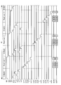
- the vertical signal line reset pulse ⁇ VCLR is applied, and the vertical signal lines 81, 82, 83, 84, 85, 86, 87, 88, 89 are reset to the VCLR potential.
- the VR1 voltage is applied from the timing generator 7 and the constant current source connection switches Si1, Si4, Si7 of the column to be output are turned on to turn on the pixel P11 among the pixels P belonging to the row to be output. , P12, P13 are selected. Subsequently, by applying the FD reset pulse ⁇ R1 from the vertical shift register 4 to each pixel P belonging to the row to be output, the potential of the FD 23 is reset, and the amplification transistors 24 of the selected pixels P11, P12, P13 are reset. Is conducted.
- the source potentials of the amplification transistors 24 of the selected pixels P11, P12, and P13 are output to the vertical signal line capacitors 81, 84, and 87, respectively, and the vertical signal line selection circuit 10 applies the vertical signal line selection pulse sc1.
- the vertical signal line selection switches S12, S45, and S78 are turned on.
- the pixel P11 is electrically connected to the vertical signal line 82
- the pixel P12 is electrically connected to the vertical signal line 85
- the pixel P13 is electrically connected to the vertical signal line 88.
- the noise voltage generated at the time of resetting is output and held on the vertical signal lines 82, 85, and 88.
- the signal charge accumulated in the PD 21 is transferred to the FD 23.
- the vertical signal line selection pulse sc3 is applied from the vertical signal line selection circuit 10
- the vertical signal line selection switches S13, S47, and S79 are turned on.
- the pixel P11 is electrically connected to the vertical signal line 83
- the pixel P12 is electrically connected to the vertical signal line 86
- the pixel P13 is electrically connected to the vertical signal line 89.
- the signal noise sum voltage in the FD 23 of the pixels P11, P12, and P13 in the first row is output and held via the amplification transistor 24 to the vertical signal lines 83, 86, and 89 that are in the floating potential state.
- the operation of reading out the noise voltage and the signal noise sum voltage from the vertical signal lines 82, 85, 88 holding the noise voltage and the vertical signal lines 83, 86, 89 holding the signal noise sum voltage is performed as follows. Is called.
- a horizontal signal line selection pulse so11 is applied from the horizontal shift register 5 to the horizontal signal line selection switches SA2 and SB3.
- the vertical signal line 82 is electrically connected to the horizontal signal line 9A
- the vertical signal line 83 is electrically connected to the horizontal signal line 9B.
- the noise voltage of the pixel P11 is read out via the horizontal signal line 9A
- the signal noise sum voltage of the pixel P11 is read out via the horizontal signal line 9B.
- a horizontal signal line selection pulse so12 is applied from the horizontal shift register 5 to the horizontal signal line selection switches SA5 and SB6.
- the vertical signal line 85 is electrically connected to the horizontal signal line 9A
- the vertical signal line 85 is electrically connected to the horizontal signal line 9B.
- the noise voltage of the pixel P12 is read out through the horizontal signal line 9A
- the signal noise sum voltage of the pixel P12 is read out through the horizontal signal line 9B.
- a horizontal signal line selection pulse so13 is applied from the horizontal shift register 5 to the horizontal signal line selection switches SA8 and SB9.
- the vertical signal line 88 is electrically connected to the horizontal signal line 9A
- the vertical signal line 88 is electrically connected to the horizontal signal line 9B.
- the noise voltage of the pixel P13 is read out via the horizontal signal line 9A
- the signal noise sum voltage of the pixel P13 is read out via the horizontal signal line 9B.
- the source potentials of the amplification transistors 24 of the selected pixels P21, P22, P23 are output to the vertical signal line capacitors 82, 85, 88, respectively, and the vertical signal line selection pulse sc2 is applied from the vertical signal line selection circuit 10.
- the vertical signal line selection switches S23, S56, and S89 are turned on.
- the pixel P21 is in conduction with the vertical signal line 83
- the pixel P22 is in communication with the vertical signal line 86
- the pixel P23 is in communication with the vertical signal line 89.
- the noise voltage generated at the time of reset is output to the vertical signal lines 83, 86 and 89 and held.
- the signal charge accumulated in the PD 21 is transferred to the FD 23.
- the vertical signal line selection pulse sc1 is applied from the vertical signal line selection circuit 10
- the vertical signal line selection switches S12, S45, and S78 are turned on.
- the pixel P21 is electrically connected to the vertical signal line 81
- the pixel P22 is electrically connected to the vertical signal line 84
- the pixel P23 is electrically connected to the vertical signal line 87.
- the signal noise sum voltage in the FD 23 of the pixels P21, P22, P23 in the first row is output and held via the amplification transistor 24 to the vertical signal lines 81, 84, 87 which are in the floating potential state.
- the horizontal signal line selection pulse so21 is applied from the horizontal shift register 5 to the horizontal signal line selection switches SA3 and SB1.
- the vertical signal line 83 is electrically connected to the horizontal signal line 9A
- the vertical signal line 81 is electrically connected to the horizontal signal line 9B.
- the noise voltage of the pixel P21 is read out through the horizontal signal line 9A
- the signal noise sum voltage of the pixel P21 is read out through the horizontal signal line 9B.
- a horizontal signal line selection pulse so22 is applied from the horizontal shift register 5 to the horizontal signal line selection switches SA6 and SB4.
- the vertical signal line 86 is electrically connected to the horizontal signal line 9A
- the vertical signal line 84 is electrically connected to the horizontal signal line 9B.
- the noise voltage of the pixel P22 is read out through the horizontal signal line 9A
- the signal noise sum voltage of the pixel P22 is read out through the horizontal signal line 9B.
- a horizontal signal line selection pulse so23 is applied from the horizontal shift register 5 to the horizontal signal line selection switches SA9 and SB7.
- the vertical signal line 89 is electrically connected to the horizontal signal line 9A
- the vertical signal line 87 is electrically connected to the horizontal signal line 9B.
- the noise voltage of the pixel P23 is read out via the horizontal signal line 9A
- the signal noise sum voltage of the pixel P23 is read out via the horizontal signal line 9B.
- the VR3 voltage is applied from the timing generator 7, and when the constant current source connection switches Si3, Si6, Si9 of the column to be output are turned on, among the pixels P belonging to the row to be output, the pixel P31, P32 and P33 are selected.
- the FD reset pulse ⁇ R3 is applied from the vertical shift register 4 to each pixel P belonging to the row to be output, so that the potential of the FD 23 is reset, and the amplification transistors 24 of the selected pixels P31, P32, and P33. Is conducted.
- the source potentials of the amplification transistors 24 of the selected pixels P31, P32, P33 are output to the vertical signal line capacitors 83, 86, 89, respectively, and the vertical signal line selection pulse sc3 is applied from the vertical signal line selection circuit 10.
- the vertical signal line selection switches S13, S47, and S79 are turned on.
- the pixel P31 is electrically connected to the vertical signal line 81
- the pixel P32 is electrically connected to the vertical signal line 84
- the pixel P33 is electrically connected to the vertical signal line 87.
- the noise voltage generated at the time of resetting is output and held on the vertical signal lines 81, 84, 87.
- the signal charge accumulated in the PD 21 is transferred to the FD 23.
- the vertical signal line selection pulse sc2 is applied from the vertical signal line selection circuit 10
- the vertical signal line selection switches S23, S56, and S89 are turned on.
- the pixel P31 is electrically connected to the vertical signal line 82
- the pixel P32 is electrically connected to the vertical signal line 86
- the pixel P33 is electrically connected to the vertical signal line 89.
- the signal noise sum voltage in the FD 23 of the pixels P31, P32, and P33 in the first row is output and held via the amplification transistor 24 to the vertical signal lines 83, 86, and 89 that are in the floating potential state.
- the horizontal signal line selection pulse so31 is applied from the horizontal shift register 5 to the horizontal signal line selection switches SA1 and SB2.
- the vertical signal line 81 is electrically connected to the horizontal signal line 9A
- the vertical signal line 83 is electrically connected to the horizontal signal line 9B.
- the noise voltage of the pixel P31 is read out through the horizontal signal line 9A
- the signal noise sum voltage of the pixel P31 is read out through the horizontal signal line 9B.
- a horizontal signal line selection pulse so32 is applied from the horizontal shift register 5 to the horizontal signal line selection switches SA4 and SB5.
- the vertical signal line 84 is electrically connected to the horizontal signal line 9A
- the vertical signal line 86 is electrically connected to the horizontal signal line 9B.
- the noise voltage of the pixel P32 is read out via the horizontal signal line 9A
- the signal noise sum voltage of the pixel P32 is read out via the horizontal signal line 9B.
- a horizontal signal line selection pulse so33 is applied from the horizontal shift register 5 to the horizontal signal line selection switches SA7 and SB8.
- the vertical signal line 87 is electrically connected to the horizontal signal line 9A
- the vertical signal line 89 is electrically connected to the horizontal signal line 9B.
- the noise voltage of the pixel P33 is read out via the horizontal signal line 9A
- the signal noise sum voltage of the pixel P33 is read out via the horizontal signal line 9B.
- the noise voltage and the signal noise sum voltage of each pixel are output and read for every third pixel P belonging to the row to be output, and finally all the pixels belonging to the row to be output are output. Output and readout of the noise voltage and the signal noise sum voltage of the pixel P are performed.
- the noise voltage generated by resetting the PD output terminal of the pixel P is applied to the vertical signal line to which the pixel P is connected.
- the signal is output by making the vertical signal line selection switch conductive to another vertical signal line connected via the selection switch.
- the signal noise sum voltage output from the pixel P is different from the vertical signal line outputting the noise voltage connected to the vertical signal line to which the pixel P is connected via another vertical signal line selection switch.
- the vertical signal line is output by turning on another vertical signal line selection switch.
- the signal voltage can be easily obtained by subtracting the noise voltage output to the other vertical signal line from the signal noise sum voltage output to one vertical signal line. Only one capacitive element is required for the vertical signal line. Therefore, as in this embodiment, by holding the noise voltage or the signal noise sum voltage in the parasitic capacitance of each vertical signal line, it is possible to have a configuration in which no additional capacitive element is provided, A signal voltage can be easily obtained by providing only one capacitive element. As a result, the noise voltage can be subtracted from the signal noise sum voltage to obtain a signal with high noise resistance, and the number of capacitive elements on the chip can be reduced to include the capacitive element portion with respect to the pixel array portion. The area ratio of the circuit portion can be reduced. In FIG. 1, C11 to C33 are schematically shown as capacitive elements provided in each vertical signal line.
- the solid-state imaging device according to the second embodiment of the present invention will be described below with reference to the drawings.
- the same components as those in the first embodiment described above are denoted by the same reference numerals, and the description thereof is omitted.
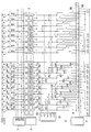
- the pixels P belonging to the same column are common vertical signal lines 81, 82, 83, 84, 85, 86, 87. , 88, 89, 90, 91, and the vertical signal lines 81, 82, 83, 84, 85, 86, 87, 88, 89, 90, 91 are connected to or disconnected from the adjacent vertical signal lines.
- Vertical signal line selection switches S12 to S91 for switching are provided.
- the vertical signal lines 81, 82, 83, 84, 85, 86, 87, 88, 89, 90, 91 are connected to the horizontal signal lines 9A, 9B via the horizontal signal line selection switches SA1 to SB0. Yes.
- the operation of outputting the noise voltage and the signal noise sum voltage to the vertical signal line in the solid-state imaging device according to the present embodiment and temporarily holding the charge in the parasitic capacitance of the vertical signal line is performed as follows.
- the vertical signal line reset pulse ⁇ VCLR is applied, and the vertical signal lines 81, 82, 83, 84, 85, 86, 87, 88, 89, 90, 91 are reset to the VCLR potential.
- the source potentials of the amplification transistors 24 of the selected pixels P11, P12, P13 are output to the vertical signal line capacitors 82, 85, 88, respectively, and the vertical signal line selection pulse sc1 is applied from the vertical signal line selection circuit 10.
- the vertical signal line selection switches S12, S45, and S78 are turned on.
- the pixel P11 is electrically connected to the vertical signal line 81
- the pixel P12 is electrically connected to the vertical signal line 84
- the pixel P13 is electrically connected to the vertical signal line 87.
- the noise voltage generated at the time of resetting is output and held on the vertical signal lines 81, 84, 87.
- the signal charge accumulated in the PD 21 is transferred to the FD 23.
- the vertical signal line selection pulse sc2 is applied from the vertical signal line selection circuit 10
- the vertical signal line selection switches S23, S56, and S89 are turned on.
- the pixel P11 is electrically connected to the vertical signal line 83
- the pixel P12 is electrically connected to the vertical signal line 86
- the pixel P13 is electrically connected to the vertical signal line 89.
- the signal noise sum voltage in the FD 23 of the pixels P11, P12, and P13 in the first row is output and held via the amplification transistor 24 to the vertical signal lines 83, 86, and 89 that are in the floating potential state.
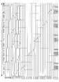
- the operation of reading out the noise voltage and the signal noise sum voltage from the vertical signal lines 81, 84, 87 holding the noise voltage and the vertical signal lines 83, 86, 89 holding the signal noise sum voltage is performed as follows. Is called.
- a horizontal signal line selection pulse so11 is applied from the horizontal shift register 5 to the horizontal signal line selection switches SA1 and SB3.
- the vertical signal line 81 is electrically connected to the horizontal signal line 9A
- the vertical signal line 83 is electrically connected to the horizontal signal line 9B.
- the noise voltage of the pixel P11 is read out via the horizontal signal line 9A
- the signal noise sum voltage of the pixel P11 is read out via the horizontal signal line 9B.
- a horizontal signal line selection pulse so12 is applied from the horizontal shift register 5 to the horizontal signal line selection switches SA4 and SB6.
- the vertical signal line 84 is electrically connected to the horizontal signal line 9A
- the vertical signal line 86 is electrically connected to the horizontal signal line 9B.
- the noise voltage of the pixel P12 is read out through the horizontal signal line 9A
- the signal noise sum voltage of the pixel P12 is read out through the horizontal signal line 9B.
- a horizontal signal line selection pulse so13 is applied from the horizontal shift register 5 to the horizontal signal line selection switches SA7 and SB9.
- the vertical signal line 87 is electrically connected to the horizontal signal line 9A
- the vertical signal line 89 is electrically connected to the horizontal signal line 9B.
- the noise voltage of the pixel P13 is read out via the horizontal signal line 9A
- the signal noise sum voltage of the pixel P13 is read out via the horizontal signal line 9B.
- the source potentials of the amplification transistors 24 of the selected pixels P21, P22, and P23 are output to the vertical signal line capacitors 83, 86, and 89, respectively, and the vertical signal line selection pulse sc2 is applied from the vertical signal line selection circuit 10.
- the vertical signal line selection switches S23, S56, and S89 are turned on.
- the pixel P21 is electrically connected to the vertical signal line 82
- the pixel P22 is electrically connected to the vertical signal line 85
- the pixel P23 is electrically connected to the vertical signal line 88.
- the noise voltage generated at the time of resetting is output and held on the vertical signal lines 82, 85, and 88.
- the signal charge accumulated in the PD 21 is transferred to the FD 23.
- the vertical signal line selection pulse sc3 is applied from the vertical signal line selection circuit 10
- the vertical signal line selection switches S34, S67, and S90 are turned on.
- the pixel P21 is electrically connected to the vertical signal line 84
- the pixel P22 is electrically connected to the vertical signal line 87
- the pixel P23 is electrically connected to the vertical signal line 90.
- the signal noise sum voltage in the FD 23 of the pixels P21, P22, and P23 in the first row is output and held via the amplification transistor 24 to the vertical signal lines 84, 87, and 90 that are in the floating potential state.
- the horizontal signal line selection pulse so21 is applied from the horizontal shift register 5 to the horizontal signal line selection switches SA2 and SB4.
- the vertical signal line 82 is electrically connected to the horizontal signal line 9A
- the vertical signal line 84 is electrically connected to the horizontal signal line 9B.
- the noise voltage of the pixel P21 is read out through the horizontal signal line 9A
- the signal noise sum voltage of the pixel P21 is read out through the horizontal signal line 9B.
- a horizontal signal line selection pulse so22 is applied from the horizontal shift register 5 to the horizontal signal line selection switches SA5 and SB7.
- the vertical signal line 85 is electrically connected to the horizontal signal line 9A
- the vertical signal line 87 is electrically connected to the horizontal signal line 9B.
- the noise voltage of the pixel P22 is read out through the horizontal signal line 9A
- the signal noise sum voltage of the pixel P22 is read out through the horizontal signal line 9B.
- a horizontal signal line selection pulse so23 is applied from the horizontal shift register 5 to the horizontal signal line selection switches SA8 and SB0.
- the vertical signal line 88 is electrically connected to the horizontal signal line 9A
- the vertical signal line 90 is electrically connected to the horizontal signal line 9B.
- the noise voltage of the pixel P23 is read out via the horizontal signal line 9A
- the signal noise sum voltage of the pixel P23 is read out via the horizontal signal line 9B.
- the VR3 voltage is applied from the timing generator 7, and when the constant current source connection switches Si3, Si6, Si9 of the column to be output are turned on, among the pixels P belonging to the row to be output, the pixel P31, P32 and P33 are selected.
- the FD reset pulse ⁇ R3 is applied from the vertical shift register 4 to each pixel P belonging to the row to be output, so that the potential of the FD 23 is reset, and the amplification transistors 24 of the selected pixels P31, P32, and P33. Is conducted.
- the source potentials of the amplification transistors 24 of the selected pixels P31, P32, and P33 are output to the vertical signal line capacitors 84, 87, and 90, respectively, and the vertical signal line selection pulse sc3 is applied from the vertical signal line selection circuit 10.
- the vertical signal line selection switches S34, S67, and S90 are turned on.
- the pixel P31 is electrically connected to the vertical signal line 83
- the pixel P32 is electrically connected to the vertical signal line 86
- the pixel P33 is electrically connected to the vertical signal line 89.
- the noise voltage generated at the time of reset is output to the vertical signal lines 83, 86 and 89 and held.
- the signal charge accumulated in the PD 21 is transferred to the FD 23.
- the vertical signal line selection pulse sc1 is applied from the vertical signal line selection circuit 10
- the vertical signal line selection switches S45, S78, S01 are turned on.
- the pixel P31 is electrically connected to the vertical signal line 85
- the pixel P32 is electrically connected to the vertical signal line 88
- the pixel P33 is electrically connected to the vertical signal line 91.
- the signal noise sum voltage in the FD 23 of the pixels P31, P32, and P33 in the first row is output and held via the amplification transistor 24 to the vertical signal lines 85, 88, and 91 that are in the floating potential state.
- the horizontal signal line selection pulse so31 is applied from the horizontal shift register 5 to the horizontal signal line selection switches SA3 and SB5.
- the vertical signal line 83 is electrically connected to the horizontal signal line 9A
- the vertical signal line 85 is electrically connected to the horizontal signal line 9B.
- the noise voltage of the pixel P31 is read out through the horizontal signal line 9A
- the signal noise sum voltage of the pixel P31 is read out through the horizontal signal line 9B.
- a horizontal signal line selection pulse so32 is applied from the horizontal shift register 5 to the horizontal signal line selection switches SA6 and SB8.
- the vertical signal line 86 is electrically connected to the horizontal signal line 9A
- the vertical signal line 88 is electrically connected to the horizontal signal line 9B.
- the noise voltage of the pixel P32 is read out via the horizontal signal line 9A
- the signal noise sum voltage of the pixel P32 is read out via the horizontal signal line 9B.
- a horizontal signal line selection pulse so33 is applied from the horizontal shift register 5 to the horizontal signal line selection switches SA9 and SB0.
- the vertical signal line 89 is electrically connected to the horizontal signal line 9A
- the vertical signal line 90 is electrically connected to the horizontal signal line 9B.
- the noise voltage of the pixel P33 is read out via the horizontal signal line 9A
- the signal noise sum voltage of the pixel P33 is read out via the horizontal signal line 9B.
- the noise voltage and the signal noise sum voltage of each pixel are output and read for every third pixel P belonging to the row to be output, and finally all the pixels belonging to the row to be output are output. Output and readout of the noise voltage and the signal noise sum voltage of the pixel P are performed.
- the noise voltage generated by resetting the PD output terminal of the pixel P is applied to the vertical signal line to which the pixel P is connected.
- the signal is output by making the vertical signal line selection switch conductive to another vertical signal line connected through the selection switch.
- the signal noise sum voltage output from the pixel P is different from the vertical signal line outputting the noise voltage connected to the vertical signal line to which the pixel P is connected via another vertical signal line selection switch.
- the vertical signal line is output by making another vertical signal line selection switch conductive.
- the signal voltage can be easily obtained by subtracting the noise voltage output to the other vertical signal line from the signal noise sum voltage output to one vertical signal line. Only one capacitive element is required for the vertical signal line. Therefore, as in the present embodiment, by holding the noise voltage or the signal noise sum voltage in the parasitic capacitance of each vertical signal line, it is possible to have a configuration in which no additional capacitive element is provided, and for each vertical signal line, A signal voltage can be easily obtained by providing only one capacitive element.
- the noise voltage can be subtracted from the signal noise sum voltage to obtain a signal with high noise resistance, and the number of capacitive elements on the chip can be reduced to include the capacitive element portion with respect to the pixel array portion.
- the area ratio of the circuit portion can be reduced.
- C11 to C33 are schematically shown as capacitive elements provided in each vertical signal line.
- the noise voltage or the signal noise sum voltage output to one vertical signal line is different from each other adjacent to the equidistant position on both sides of the vertical signal line. Since the signal is output to the vertical signal line, the length of the wiring for holding each voltage can be made substantially equal. Therefore, when the wiring is used as a capacitive element, there is an advantage that the capacity of the wiring for holding each voltage can be made uniform and the accuracy can be improved.
- the pixels P belonging to the same column are common vertical signal lines 80, 81, 82, 83, 84, 85, 86. , 87...
- the noise voltage and the signal noise sum voltage of every fifth pixel for all the pixels P belonging to the output target row. Are output and read out. Therefore, a description will be given below of a procedure for outputting and reading out the noise voltage and the signal noise sum voltage for the pixels P11 to P51 among all the pixels P belonging to the row to be output. For other pixels belonging to the row to be output, the noise voltage and the signal noise sum voltage are output and read out in the same procedure, so the description thereof is omitted.
- Each of the vertical signal lines 80, 81, 82, 83, 84, 85, 86, 87, 88 is provided with vertical signal line selection switches S01 to S78 for switching conduction or disconnection between the adjacent vertical signal lines.
- the vertical signal lines 80, 81, 82, 83, 84, 85, 86, 87, 88 are connected to the horizontal signal lines 9A, 9B via horizontal signal line selection switches SA1 to SB7.
- a driving method of the solid-state imaging device configured as described above will be described with reference to the timing chart of FIG.
- the output of the noise voltage and the signal noise sum voltage of each pixel for every fifth pixel P belonging to the row to be output and Read.
- the operation of outputting the noise voltage and the signal noise sum voltage to the vertical signal line in the solid-state imaging device according to this embodiment and temporarily holding the charge in the parasitic capacitance of the vertical signal line is performed as follows.
- the vertical signal line reset pulse ⁇ VCLR is applied, and the FD 23 and the vertical signal lines 80, 81, 82, 83, 84, 85, 86, 87, 88 are reset to the VCLR potential.
- the VR1 voltage is applied from the timing generator 7, and when the constant current source connection switch Si1 of the column to be output is turned on, the pixel P11 is selected from among the pixels P belonging to the row to be output. . Subsequently, when the FD reset pulse ⁇ R1 is applied from the vertical shift register 4 to each pixel P belonging to the row to be output, the potential of the FD 23 is reset, and the amplification transistor 24 of the selected pixel P11 becomes conductive.
- the source potential of the amplification transistor 24 of the selected pixel P11 is output to the vertical signal line capacitors 82 and 87, respectively, and vertical signal line selection pulses sc1 and sc4 are applied from the vertical signal line selection circuit 10, thereby causing the vertical potential.
- the signal line selection switches S01 and S34 are turned on.
- the vertical signal line selection pulse sc2 is applied from the vertical signal line selection circuit 10, and the vertical signal line selection switch S12 is turned on.
- the pixel P11 becomes conductive with the vertical signal lines 80 and 81, and the noise voltage generated at the time of resetting of the FD 23 or the like is output to the vertical signal lines 80 and 81. Thereafter, the vertical signal line selection switch S12 is turned off.
- the vertical signal line selection pulse sc3 is applied from the vertical signal line selection circuit 10 with the vertical signal line selection pulses sc1 and sc4 being applied, the vertical signal line selection switch S23 is turned on.
- the pixel P11 becomes conductive with the vertical signal lines 83 and 84.
- the signal noise sum voltage in the FD 23 of the pixel P11 is output and held via the amplification transistor 24 to the vertical signal lines 83 and 84 that are in the floating potential state.
- the operation of reading out the noise voltage and the signal noise sum voltage from the vertical signal lines 80 and 81 holding the noise voltage and the vertical signal lines 83 and 84 holding the signal noise sum voltage is performed as follows.
- the horizontal shift register 5 applies the horizontal signal line selection pulse so11 to the horizontal signal line selection switches SA0 and SB3.
- the vertical signal lines 80 and 81 are electrically connected to the horizontal signal line 9A
- the vertical signal lines 83 and 84 are electrically connected to the horizontal signal line 9B.
- the noise voltage of the pixel P11 is read out via the horizontal signal line 9A
- the signal noise sum voltage of the pixel P11 is read out via the horizontal signal line 9B.
- the pixel P21 is selected among the pixels P belonging to the row to be output. Subsequently, when the FD reset pulse ⁇ R2 is applied from the vertical shift register 4 to each pixel P belonging to the row to be output, the potential of the FD 23 is reset, and the amplification transistor 24 of the selected pixel P21 becomes conductive.
- the source potential of the amplification transistor 24 of the selected pixel P21 is output to the vertical signal line capacitors 83 and 88, respectively, and vertical signal line selection pulses sc2 and sc5 are applied from the vertical signal line selection circuit 10, thereby causing the vertical potential.
- the signal line selection switches S12 and S45 are turned on.
- the vertical signal line selection pulse sc3 is applied from the vertical signal line selection circuit 10, and the vertical signal line selection switch S23 is turned on.
- the pixel P21 becomes conductive with the vertical signal lines 81 and 82, and the noise voltage generated at the time of resetting the FD 23 or the like is output to the vertical signal lines 81 and 82. Thereafter, the vertical signal line selection switch S23 is turned off.
- the vertical signal line selection pulse sc4 is applied from the vertical signal line selection circuit 10 while the vertical signal line selection pulses sc2 and sc5 are applied, the vertical signal line selection switch S34 is turned on.
- the pixel P21 is brought into conduction with the vertical signal lines 84 and 85.
- the signal noise sum voltage in the FD 23 of the pixel P21 is output and held via the amplification transistor 24 to the vertical signal lines 84 and 85 that are in the floating potential state.
- the operation of reading out the noise voltage and the signal noise sum voltage from the vertical signal lines 81 and 82 holding the noise voltage and the vertical signal lines 84 and 85 holding the signal noise sum voltage is performed as follows.
- the horizontal shift register 5 applies the horizontal signal line selection pulse so21 to the horizontal signal line selection switches SA1 and SB4.
- the vertical signal lines 81 and 82 are electrically connected to the horizontal signal line 9A
- the vertical signal lines 84 and 85 are electrically connected to the horizontal signal line 9B.
- the noise voltage of the pixel P21 is read out through the horizontal signal line 9A
- the signal noise sum voltage of the pixel P21 is read out through the horizontal signal line 9B.
- the VR3 voltage is applied from the timing generator 7, and when the constant current source connection switch Si3 of the column to be output is turned on, the pixel P31 is selected from the pixels P belonging to the row to be output. Subsequently, when the FD reset pulse ⁇ R3 is applied from the vertical shift register 4 to each pixel P belonging to the row to be output, the potential of the FD 23 is reset, and the amplification transistor 24 of the selected pixel P31 becomes conductive.
- the source potential of the amplification transistor 24 of the selected pixel P31 is output to the vertical signal line capacitors 84 and 89, respectively, and vertical signal line selection pulses sc3 and sc1 are applied from the vertical signal line selection circuit 10, thereby causing the vertical potential.
- the signal line selection switches S23 and S56 are turned on.
- the vertical signal line selection pulse sc4 is applied from the vertical signal line selection circuit 10, and the vertical signal line selection switch S34 is turned on.
- the pixel P31 becomes conductive with the vertical signal lines 82 and 83, and the noise voltage generated at the time of resetting the FD 23 or the like is output to the vertical signal lines 82 and 83.
- the vertical signal line selection switch S34 is turned off.
- the vertical signal line selection pulse sc5 is applied from the vertical signal line selection circuit 10 with the vertical signal line selection pulses sc3 and sc1 being applied, the vertical signal line selection switch S45 is turned on.
- the pixel P31 becomes conductive with the vertical signal lines 85 and 86.
- the signal noise sum voltage in the FD 23 of the pixel P31 is output and held via the amplification transistor 24 to the vertical signal lines 85 and 86 that are in the floating potential state.
- the operation of reading out the noise voltage and the signal noise sum voltage from the vertical signal lines 82 and 83 holding the noise voltage and the vertical signal lines 85 and 86 holding the signal noise sum voltage is performed as follows.
- the horizontal shift register 5 applies the horizontal signal line selection pulse so31 to the horizontal signal line selection switches SA2 and SB5. Accordingly, the vertical signal lines 82 and 83 are electrically connected to the horizontal signal line 9A, and the vertical signal lines 85 and 86 are electrically connected to the horizontal signal line 9B.
- the noise voltage of the pixel P31 is read out through the horizontal signal line 9A, and the signal noise sum voltage of the pixel P31 is read out through the horizontal signal line 9B.
- the VR4 voltage is applied from the timing generator 7, and the constant current source connection switch Si4 of the row to be output is turned on to select the pixel P41 among the pixels P belonging to the row to be output.
- the FD reset pulse ⁇ R3 is applied from the vertical shift register 4 to each pixel P belonging to the row to be output, the potential of the FD 23 is reset, and the amplification transistor 24 of the selected pixel P41 becomes conductive.
- the source potential of the amplification transistor 24 of the selected pixel P41 is output to the vertical signal line capacitor 85, and vertical signal line selection pulses sc4 and sc2 are applied from the vertical signal line selection circuit 10 to thereby generate vertical signal lines.
- the selection switches S34 and S67 are turned on.
- the vertical signal line selection pulse sc5 is applied from the vertical signal line selection circuit 10, and the vertical signal line selection switch S45 is turned on.
- the vertical signal line selection switch S45 is turned off.
- the vertical signal line selection switch S56 is turned on.
- the pixel P31 is brought into conduction with the vertical signal lines 86 and 87.
- the signal noise sum voltage in the FD 23 of the pixel P41 is output and held via the amplification transistor 24 to the vertical signal lines 86 and 87 that are in the floating potential state.
- the operation of reading out the noise voltage and the signal noise sum voltage from the vertical signal lines 83 and 84 holding the noise voltage and the vertical signal lines 86 and 87 holding the signal noise sum voltage is performed as follows.
- the horizontal shift register 5 applies the horizontal signal line selection pulse so41 to the horizontal signal line selection switches SA3 and SB6.
- the vertical signal lines 83 and 84 are electrically connected to the horizontal signal line 9A
- the vertical signal lines 86 and 87 are electrically connected to the horizontal signal line 9B.
- the noise voltage of the pixel P41 is read out via the horizontal signal line 9A
- the signal noise sum voltage of the pixel P41 is read out via the horizontal signal line 9B.
- the VR5 voltage is applied from the timing generator 7 and the constant current source connection switch Si5 of the column to be output is turned on to select the pixel P51 among the pixels P belonging to the row to be output.
- the FD reset pulse ⁇ R3 is applied from the vertical shift register 4 to each pixel P belonging to the row to be output, the potential of the FD 23 is reset, and the amplification transistor 24 of the selected pixel P51 becomes conductive.
- the source potential of the amplification transistor 24 of the selected pixel P51 is output to the vertical signal line capacitor 86, and vertical signal line selection pulses sc5 and sc3 are applied from the vertical signal line selection circuit 10 to thereby generate vertical signal lines.
- the selection switches S45 and S78 are turned on.
- the vertical signal line selection pulse sc1 is applied from the vertical signal line selection circuit 10, and the vertical signal line selection switch S56 is turned on.
- the vertical signal line selection switch S56 is turned off.
- the signal charge accumulated in the PD 21 is transferred to the FD 23.
- the vertical signal line selection pulse sc2 is applied from the vertical signal line selection circuit 10 with the vertical signal line selection pulses sc5 and sc3 being applied, the vertical signal line selection switch S67 is turned on. Thereby, among the pixels P belonging to the row to be output, the pixel P51 is brought into conduction with the vertical signal lines 87 and 88. The signal noise sum voltage in the FD 23 of the pixel P51 is output and held via the amplification transistor 24 to the vertical signal lines 87 and 88 that are in the floating potential state.
- the operation of reading out the noise voltage and the signal noise sum voltage from the vertical signal lines 84 and 85 holding the noise voltage and the vertical signal lines 87 and 88 holding the signal noise sum voltage is performed as follows.
- the horizontal shift register 5 applies the horizontal signal line selection pulse so51 to the horizontal signal line selection switches SA4 and SB7.
- the vertical signal lines 84 and 85 are electrically connected to the horizontal signal line 9A
- the vertical signal lines 87 and 88 are electrically connected to the horizontal signal line 9B.
- the noise voltage of the pixel P51 is read out via the horizontal signal line 9A
- the signal noise sum voltage of the pixel P51 is read out via the horizontal signal line 9B.
- the noise voltage generated by resetting the PD output terminal of the pixel P is applied to the vertical signal line to which the pixel P is connected.
- the signal is output by making the vertical signal line selection switch conductive to the other two vertical signal lines connected via the selection switch.
- the signal noise sum voltage output from the pixel P is different from the vertical signal line outputting the noise voltage connected to the vertical signal line to which the pixel P is connected via another vertical signal line selection switch.
- the two vertical signal lines are outputted by making another vertical signal line selection switch conductive.
- the noise voltage and the signal noise sum voltage are output to two vertical signal lines connected in parallel, but instead, are output to three or more vertical signal lines. May be.
Landscapes
- Engineering & Computer Science (AREA)
- Multimedia (AREA)
- Signal Processing (AREA)
- Transforming Light Signals Into Electric Signals (AREA)
- Solid State Image Pick-Up Elements (AREA)
Abstract
ノイズ耐性の高い信号を維持しつつ、チップ上の容量素子の数を低減して画素アレイ部に対して容量素子部を含む周辺回路部の面積比率を小さくする。 2次元的に配列された複数の単位画素と、複数の単位画素からなる複数の画素グループがそれぞれ共通に接続された複数の転送線と、各該転送線と他の2以上の転送線との導通および切断を切り替える複数のスイッチとを備え、各前記単位画素が、入射光を光電変換する光電変換素子と光電変換した電荷を電圧変換する電荷電圧変換素子とを含み、該電荷電圧変換をリセットする際に発生するノイズ電圧と、該ノイズ電圧に光電変換により発生した信号電荷を加えた信号ノイズ和電圧とを、該単位画素を含む画素グループの属する前記転送線に前記スイッチを介して接続された他の異なる転送線にそれぞれ出力する固体撮像装置を提供する。
Description
本発明は、固体撮像装置に関するものである。
従来、CMOS(complementary metal-oxide semiconductor)イメージセンサに代表されるような、光電変換素子が蓄積した信号電荷を画素内において信号電圧に変換してから信号線に出力する増幅型固体撮像装置が知られている(例えば、特許文献1参照。)。この固体撮像装置は、画素内の電荷電圧変換素子をリセットする際に発生する電圧(以下、ノイズ電圧という。)と、該ノイズ電圧に、光電変換により発生した信号電荷を加えた電圧(以下、信号ノイズ和電圧という。)とを画素内の電荷電圧変換素子から出力させて、別々に保持させる2つの容量素子を全ての垂直信号線に備えている。
そして、この固体撮像装置は、垂直シフトレジスタにより選択された行の全ての画素からノイズ電圧と信号ノイズ和電圧とを容量素子に保持した後に、水平シフトレジスタにより選択された列に備えられた2つの容量素子から、ノイズ電圧と信号ノイズ和電圧とを順次出力させるようになっている。
しかしながら、特許文献1の固体撮像装置は、垂直信号線の本数の2倍の数の容量素子をCMOSイメージセンサのチップ上に備えているために、画素アレイに対して容量素子部を含む周辺回路部の面積比率が大きくなる。
本発明は、上述した事情に鑑みてなされたものであって、ノイズ耐性の高い信号を維持しつつ、チップ上の容量素子の数を低減して画素アレイ部に対して容量素子部を含む周辺回路部の面積比率を小さくすることができる固体撮像装置を提供することを目的とする。
上記目的を達成するために、本発明は以下の手段を提供する。
本発明の一態様は、2次元的に配列された複数の単位画素と、1以上の単位画素からなる複数の画素グループがそれぞれ共通に接続された複数の転送線と、各該転送線と他の2以上の転送線との導通および切断を切り替える複数のスイッチとを備え、各前記単位画素が、入射光を光電変換する光電変換素子と光電変換された信号電荷を電圧変換する電荷電圧変換素子とを含み、該電荷電圧変換素子をリセットする際に発生するノイズ電圧と、該ノイズ電圧に光電変換により発生した信号電圧を加えた信号ノイズ和電圧とを、該単位画素を含む画素グループの属する前記転送線に前記スイッチを介して接続された他の異なる転送線にそれぞれ出力する固体撮像装置である。
本発明の一態様は、2次元的に配列された複数の単位画素と、1以上の単位画素からなる複数の画素グループがそれぞれ共通に接続された複数の転送線と、各該転送線と他の2以上の転送線との導通および切断を切り替える複数のスイッチとを備え、各前記単位画素が、入射光を光電変換する光電変換素子と光電変換された信号電荷を電圧変換する電荷電圧変換素子とを含み、該電荷電圧変換素子をリセットする際に発生するノイズ電圧と、該ノイズ電圧に光電変換により発生した信号電圧を加えた信号ノイズ和電圧とを、該単位画素を含む画素グループの属する前記転送線に前記スイッチを介して接続された他の異なる転送線にそれぞれ出力する固体撮像装置である。
本態様によれば、一の単位画素の電荷電圧変換素子をリセットすることにより発生したノイズ電圧は、当該単位画素が接続された転送線にスイッチを介して接続された他の転送線に、当該スイッチを導通させることによって出力される。一方、一の単位画素から出力された信号ノイズ和電圧は、当該単位画素が接続された転送線に他のスイッチを介して接続された、ノイズ電圧を出力した転送線とは異なる転送線に、当該他のスイッチを導通させることによって出力される。
すなわち、信号電圧は、一の転送線に出力された信号ノイズ和電圧から他の転送線に出力されたノイズ電圧を減算することにより、簡単に取得することができ、この場合に、各転送線に設ける容量要素(例えば、容量素子あるいは転送線の寄生容量)は1個で済む。
その結果、信号ノイズ和電圧からノイズ電圧を減算して、ノイズ耐性の高い信号を得ることができるとともに、チップ上の容量素子の数を低減して画素アレイ部に対して容量素子部を含む周辺回路部の面積比率を小さくすることができる。
その結果、信号ノイズ和電圧からノイズ電圧を減算して、ノイズ耐性の高い信号を得ることができるとともに、チップ上の容量素子の数を低減して画素アレイ部に対して容量素子部を含む周辺回路部の面積比率を小さくすることができる。
上記態様においては、各前記スイッチが、前記転送線と、その転送線に対して等距離に配置されている複数の他の転送線とを接続する配線にそれぞれ設けられていてもよい。
このようにすることで、転送線間を接続する配線および転送線によって構成される寄生容量をほぼ等しくすることができ、高い精度で信号電圧を得ることができる。
このようにすることで、転送線間を接続する配線および転送線によって構成される寄生容量をほぼ等しくすることができ、高い精度で信号電圧を得ることができる。
また、上記態様においては、各前記スイッチは、各前記単位画素から出力される前記ノイズ電圧および前記信号ノイズ和電圧が、それぞれ複数の前記他の転送線に出力されるように設けられていてもよい。
このようにすることで、ノイズ電圧および信号ノイズ和電圧を保持する容量要素の容量を増加させることができる。特に、寄生容量を容量要素として利用する場合には効果的である。
このようにすることで、ノイズ電圧および信号ノイズ和電圧を保持する容量要素の容量を増加させることができる。特に、寄生容量を容量要素として利用する場合には効果的である。
このようにすることで、2次元的に配列された複数の単位画素が、3以上の転送線をそれぞれ含む複数のグループに分けられ、制御部は、各グループにおいていずれかの単位画素を択一的に選択し、スイッチを操作してノイズ電圧を第1の他の転送線に出力して保持させ、スイッチを操作して信号ノイズ和電圧を第2の他の転送線に出力して保持させ、これら2つの転送線に保持されているノイズ電圧および信号ノイズ和電圧を読み出す。そして、選択する単位画素を順次切り替えて上記動作を繰り返すことにより、全ての単位画素から、ノイズ耐性の高い信号を得ることができる。
また、上記態様においては、前記単位画素に接続された電源電圧を、前記単位画素からの電圧出力を可能な状態にするイネーブル電位と、前記単位画素からの電圧出力を停止した状態にするディスエーブル電位とに切り替える電源電圧切替手段を備え、前記制御部が、選択された単位画素からのノイズ電圧および信号ノイズ和電圧を出力させる際に、当該単位画素に供給する電源電圧をイネーブル電位とし、同一グループ内の他の前記単位画素に供給する電源電圧をディスエーブル電位とするように前記電源電圧切替手段を制御する。
このようにすることで、選択されていない単位画素に対してノイズ電圧あるいは信号ノイズ和電圧の出力を指示しても、電源電圧がディスエーブル電位に設定されている単位画素からの電圧出力は行われず、電源電圧がイネーブル電位に設定されている単位画素のみから電圧出力が行われる。
本発明によれば、ノイズ耐性の高い信号を維持しつつ、チップ上の容量素子の数を低減して画素アレイ部に対して容量素子部を含む周辺回路部の面積比率を小さくすることができる固体撮像装置を提供することが可能となる。
(第1の実施形態)
以下に、本発明の第1の実施形態に係る固体撮像装置について図面を参照して説明する。
図1に示すように、本実施形態に係る固体撮像装置は、複数の画素Pを備える画素アレイ3、垂直シフトレジスタ4、水平シフトレジスタ5、タイミングジェネレータ(電源電圧切替手段)7、垂直信号線選択回路10及び制御回路(制御部)11を備えている。
以下に、本発明の第1の実施形態に係る固体撮像装置について図面を参照して説明する。
図1に示すように、本実施形態に係る固体撮像装置は、複数の画素Pを備える画素アレイ3、垂直シフトレジスタ4、水平シフトレジスタ5、タイミングジェネレータ(電源電圧切替手段)7、垂直信号線選択回路10及び制御回路(制御部)11を備えている。
画素アレイ3は、複数の画素Pが行列状、すなわち行方向と列方向に所定数配列されたものであり、同一の列に属する画素Pは共通の垂直信号線81,82,83,84,85,86,87,88,89に接続されている。各垂直信号線81,82,83,84,85,86,87,88,89は水平信号線選択スイッチSA1~SB9(後述)を介して共通の水平信号線9A,9Bに接続されて、定電流源接続スイッチSi1~Si9(後述)を介して定電流源Ic1~Ic9に接続されている。
垂直シフトレジスタ4は、画素アレイ3の中から一の行を選択し、選択した行に属する画素Pに後述するパルスφRj,φTjを入力することにより、各画素Pから垂直信号線81,82,83,84,85,86,87,88,89へ信号を出力させる。
水平シフトレジスタ5は、水平信号線選択スイッチSA1~SB9(後述)に対して水平信号線選択パルスso11~so33を入力することにより、水平信号線選択パルスに従って水平信号線選択スイッチSA1~SB9を駆動させて垂直信号線81,82,83,84,85,86,87,88,89から水平信号線9A,9Bへ信号を出力させる。
垂直信号線81,82,83,84,85,86,87,88,89には、各垂直信号線81,82,83,84,85,86,87,88,89と定電流源Ic1~Ic9とを接続し、垂直信号線と定電流源との導通および切断を切り替える定電流源接続スイッチSi1~Si9と、各垂直信号線81,82,83,84,85,86,87,88,89と他の垂直信号線81,82,83,84,85,86,87,88,89とを接続し、接続した垂直信号線81,82,83,84,85,86,87,88,89同士の導通および切断を切り替える垂直信号線選択スイッチS12~S89と、各垂直信号線81,82,83,84,85,86,87,88,89と水平信号線9A,9Bとの導通および切断を切り替える水平信号線選択スイッチSA1~SB9とが設けられている。定電流源接続スイッチSi1~Si9と垂直信号線選択スイッチS12~S89は、後述する垂直信号線選択回路10からの垂直信号線選択パルスsc1~sc3に基づいて駆動する。
タイミングジェネレータ7は、各画素Pに電源電圧を供給する電源を含み、各画素Pの電源電圧を、画素Pの電圧出力を可能な状態にするイネーブル電位と、画素Pの電圧出力を停止した状態にするディスエーブル電位とに切り替える。後述する制御回路7からの制御信号に基づく電圧パルスVR1~VR3に従って、各画素Pに電源電圧を供給し、電源電圧を供給した各画素Pが接続されている各垂直信号線の定電流源接続スイッチをオン状態にする。
本実施形態においては、電圧パルスVR1が供給された場合には画素P11,P12,P13の電圧出力が可能となり、電圧パルスVR2が供給された場合には画素P21,P22,P23の電圧出力が可能となり、電圧パルスVR3が供給された場合には画素P31,P32,P33の電圧出力が可能となる。
本実施形態においては、電圧パルスVR1が供給された場合には画素P11,P12,P13の電圧出力が可能となり、電圧パルスVR2が供給された場合には画素P21,P22,P23の電圧出力が可能となり、電圧パルスVR3が供給された場合には画素P31,P32,P33の電圧出力が可能となる。
なお、画素Pの電圧出力を可能な状態とするためには画素Pに例えば3.3V程度の電源電圧を供給し、画素Pの電圧出力を停止した状態にするためには画素Pに対して後述する各画素Pの転送トランジスタ22がオンとならない1.0V程度の電源電圧を供給する。
垂直信号線選択回路10は、垂直信号線選択スイッチS12~S89に対して垂直信号線選択パルスsc1~sc3を出力し、垂直信号線選択スイッチS12~S89を駆動する。
制御回路11は、予め設定されたパルスシーケンスに従い、上述した各パルスを出力させる制御信号を垂直シフトレジスタ4、水平シフトレジスタ5、タイミングジェネレータ7及び垂直信号線選択回路10に出力することにより、画素アレイ3からの信号の読み出し動作を制御する。
次に、各画素Pの回路構成について図2を参照して説明する。
画素Pは、受光した光信号を光電変換して信号電荷を蓄積するフォトダイオード(PD、光電変換素子)21、該PD21に蓄積された信号電荷を転送する転送トランジスタ22、該転送トランジスタ22によって転送された信号電荷を電圧変換するフローティングディフュージョン(FD、電荷電圧変換素子)23、FD23に蓄積された信号電荷を電圧として読み出す増幅トランジスタ24、φTjと転送トランジスタ22との間に接続された画素選択トランジスタ25およびFD23の電圧をリセットするFDリセットトランジスタ26を備えている。
画素Pは、受光した光信号を光電変換して信号電荷を蓄積するフォトダイオード(PD、光電変換素子)21、該PD21に蓄積された信号電荷を転送する転送トランジスタ22、該転送トランジスタ22によって転送された信号電荷を電圧変換するフローティングディフュージョン(FD、電荷電圧変換素子)23、FD23に蓄積された信号電荷を電圧として読み出す増幅トランジスタ24、φTjと転送トランジスタ22との間に接続された画素選択トランジスタ25およびFD23の電圧をリセットするFDリセットトランジスタ26を備えている。
増幅トランジスタ24は、ゲートに接続されたFD23の信号電圧を増幅し、その信号をソース側の垂直信号線8に出力する。具体的には、任意の列のVR電圧が3.3Vのときに垂直シフトレジスタ4からFDリセットトランジスタ26のゲートにFDリセットパルスφRjが入力されることにより、増幅トランジスタ24のゲートがアクティブ状態となり、読み出し画素の選択が行われる。同時に、FD23に転送された信号電荷は、FDリセットトランジスタ26のドレイン側に排出される。これによりFD23の電圧がリセットされる。
転送トランジスタ22は、画素選択トランジスタ25を介してゲートに転送パルスφTjが入力されることにより、ソース側のPD21からドレイン側のFD23へ、PD21が蓄積した信号電荷を転送する。転送トランジスタ22へのφTj信号はVRの電圧に応じて選択トランジスタ25が導通および非導通状態となることにより、列毎に選択される。この転送動作によりPD21が蓄積していた信号電荷量はゼロにリセットされる。FD23は、転送トランジスタ22を介してPD21から転送されてきた信号電荷に応じた信号電圧を生成する。
次に、このように構成された固体撮像装置の駆動方法について図3のタイミングチャートを参照して説明する。
本実施形態に係る固体撮像装置は、画素Pが受光した光信号に係る電圧と、FD23のリセットの際に生じたノイズに係る電圧(以下、「ノイズ電圧」という)とを読み出す。ここで、画素Pが受光した光信号に係る電圧には、上記したFD23のリセットの際に生じたノイズに係る電圧が含まれている。従って、本実施形態に係る固体撮像装置においては、ノイズ電圧と、画素Pが受光した光信号に係る電圧にノイズ電圧を加えた電圧(以下、「信号ノイズ和電圧」という)とを読み出す。
本実施形態に係る固体撮像装置は、画素Pが受光した光信号に係る電圧と、FD23のリセットの際に生じたノイズに係る電圧(以下、「ノイズ電圧」という)とを読み出す。ここで、画素Pが受光した光信号に係る電圧には、上記したFD23のリセットの際に生じたノイズに係る電圧が含まれている。従って、本実施形態に係る固体撮像装置においては、ノイズ電圧と、画素Pが受光した光信号に係る電圧にノイズ電圧を加えた電圧(以下、「信号ノイズ和電圧」という)とを読み出す。
ノイズ電圧及び信号ノイズ和電圧の読み出しは、ノイズ電圧及び信号ノイズ和電圧を何れかの垂直信号線に出力し、垂直信号線の寄生容量にその電荷をいったん保持させる動作と、保持させた電荷を読み出す動作の概ね2つの動作に分類することができる。
まずノイズ電圧及び信号ノイズ和電圧を垂直信号線に出力し、垂直信号線の寄生容量にその電荷をいったん保持させる動作は以下のように行われる。
なお、初期状態においては、垂直信号線リセットパルスφVCLRが印加され、垂直信号線81,82,83,84,85,86,87,88,89がVCLR電位にリセットされた状態とする。
なお、初期状態においては、垂直信号線リセットパルスφVCLRが印加され、垂直信号線81,82,83,84,85,86,87,88,89がVCLR電位にリセットされた状態とする。
この状態において、タイミングジェネレータ7からVR1電圧が印加され、出力対象となる列の定電流源接続スイッチSi1,Si4,Si7がオンすることにより出力対象となる行に属する各画素Pのうち、画素P11,P12,P13が選択される。続いて、垂直シフトレジスタ4から出力対象となる行に属する各画素PにFDリセットパルスφR1が印加されることで、FD23の電位がリセットされ、選択された画素P11,P12,P13の増幅トランジスタ24が導通する。
そして、選択された画素P11,P12,P13の増幅トランジスタ24のソース電位は垂直信号線容量81、84、87にそれぞれ出力され、垂直信号線選択回路10から垂直信号線選択パルスsc1が印加されることにより、垂直信号線選択スイッチS12,S45,S78がオンとなる。これにより、出力対象となる行に属する各画素Pのうち、画素P11は垂直信号線82と、画素P12は垂直信号線85と、画素P13は垂直信号線88と導通した状態となり、FD23等のリセット時に生じたノイズ電圧が垂直信号線82,85,88に出力され保持される。
続いて、垂直シフトレジスタ4により選択された行に電荷転送パルスφTが印加されることで、PD21に蓄積された信号電荷がFD23に転送される。その後、垂直信号線選択回路10から垂直信号線選択パルスsc3が印加されることにより、垂直信号線選択スイッチS13,S47,S79がオンとなる。これにより、出力対象となる行に属する各画素Pのうち、画素P11は垂直信号線83と、画素P12は垂直信号線86と、画素P13は垂直信号線89と導通した状態となる。1行目の画素P11,P12,P13のFD23における信号ノイズ和電圧が増幅トランジスタ24を介して浮遊電位状態とされている垂直信号線83,86,89に出力され保持される。
そして、ノイズ電圧を保持した垂直信号線82,85,88および信号ノイズ和電圧を保持した垂直信号線83,86,89とから、ノイズ電圧及び信号ノイズ和電圧とを読み出す動作は以下のよう行われる。
水平シフトレジスタ5から水平信号線選択パルスso11を水平信号線選択スイッチSA2,SB3に印加する。これにより垂直信号線82が水平信号線9Aと導通し、垂直信号線83が水平信号線9Bと導通する。そして、画素P11のノイズ電圧が水平信号線9Aを介して読み出され、画素P11の信号ノイズ和電圧が水平信号線9Bを介して読み出される。
水平シフトレジスタ5から水平信号線選択パルスso11を水平信号線選択スイッチSA2,SB3に印加する。これにより垂直信号線82が水平信号線9Aと導通し、垂直信号線83が水平信号線9Bと導通する。そして、画素P11のノイズ電圧が水平信号線9Aを介して読み出され、画素P11の信号ノイズ和電圧が水平信号線9Bを介して読み出される。
同様に、水平シフトレジスタ5から水平信号線選択パルスso12を水平信号線選択スイッチSA5,SB6に印加する。これにより垂直信号線85が水平信号線9Aと導通し、垂直信号線85が水平信号線9Bと導通する。そして、画素P12のノイズ電圧が水平信号線9Aを介して読み出され、画素P12の信号ノイズ和電圧が水平信号線9Bを介して読み出される。
同様に、水平シフトレジスタ5から水平信号線選択パルスso13を水平信号線選択スイッチSA8,SB9に印加する。これにより垂直信号線88が水平信号線9Aと導通し、垂直信号線88が水平信号線9Bと導通する。そして、画素P13のノイズ電圧が水平信号線9Aを介して読み出され、画素P13の信号ノイズ和電圧が水平信号線9Bを介して読み出される。
続いて、タイミングジェネレータ7からVR2電圧が印加され、出力対象となる列の定電流源接続スイッチSi2,Si5,Si8がオンすることにより、出力対象となる行に属する各画素Pのうち、画素P21,P22,P23が選択される。続いて、垂直シフトレジスタ4から出力対象となる行に属する各画素PにFDリセットパルスφR2が印加されることで、FD23の電位がリセットされ、選択された画素P21,P22,P23の増幅トランジスタ24が導通する。
そして、選択された画素P21,P22,P23の増幅トランジスタ24のソース電位は垂直信号線容量82、85、88にそれぞれ出力され、垂直信号線選択回路10から垂直信号線選択パルスsc2が印加されることにより、垂直信号線選択スイッチS23,S56,S89がオンとなる。これにより、出力対象となる行に属する各画素Pのうち、画素P21は垂直信号線83と、画素P22は垂直信号線86と、画素P23は垂直信号線89と導通した状態となり、FD23等のリセット時に生じたノイズ電圧が垂直信号線83,86,89に出力され保持される。
続いて、垂直シフトレジスタ4により選択された行に電荷転送パルスφTが印加されることで、PD21に蓄積された信号電荷がFD23に転送される。その後、垂直信号線選択回路10から垂直信号線選択パルスsc1が印加されることにより、垂直信号線選択スイッチS12,S45,S78がオンとなる。これにより、出力対象となる行に属する各画素Pのうち、画素P21は垂直信号線81と、画素P22は垂直信号線84と、画素P23は垂直信号線87と導通した状態となる。1行目の画素P21,P22,P23のFD23における信号ノイズ和電圧が増幅トランジスタ24を介して浮遊電位状態とされている垂直信号線81,84,87に出力され保持される。
そして、ノイズ電圧を保持した垂直信号線83,86,89および信号ノイズ和電圧を保持した垂直信号線81,84,87とから、ノイズ電圧及び信号ノイズ和電圧とを読み出す動作は以下のよう行われる。
水平シフトレジスタ5から水平信号線選択パルスso21を水平信号線選択スイッチSA3,SB1に印加する。これにより垂直信号線83が水平信号線9Aと導通し、垂直信号線81が水平信号線9Bと導通する。そして、画素P21のノイズ電圧が水平信号線9Aを介して読み出され、画素P21の信号ノイズ和電圧が水平信号線9Bを介して読み出される。
同様に、水平シフトレジスタ5から水平信号線選択パルスso22を水平信号線選択スイッチSA6,SB4に印加する。これにより垂直信号線86が水平信号線9Aと導通し、垂直信号線84が水平信号線9Bと導通する。そして、画素P22のノイズ電圧が水平信号線9Aを介して読み出され、画素P22の信号ノイズ和電圧が水平信号線9Bを介して読み出される。
同様に、水平シフトレジスタ5から水平信号線選択パルスso23を水平信号線選択スイッチSA9,SB7に印加する。これにより垂直信号線89が水平信号線9Aと導通し、垂直信号線87が水平信号線9Bと導通する。そして、画素P23のノイズ電圧が水平信号線9Aを介して読み出され、画素P23の信号ノイズ和電圧が水平信号線9Bを介して読み出される。
続いて、タイミングジェネレータ7からVR3電圧が印加され、出力対象となる列の定電流源接続スイッチSi3,Si6,Si9がオンすることにより出力対象となる行に属する各画素Pのうち、画素P31,P32,P33が選択される。続いて、垂直シフトレジスタ4から出力対象となる行に属する各画素PにFDリセットパルスφR3が印加されることで、FD23の電位がリセットされ、選択された画素P31,P32,P33の増幅トランジスタ24が導通する。
そして、選択された画素P31,P32,P33の増幅トランジスタ24のソース電位は垂直信号線容量83、86、89にそれぞれ出力され、垂直信号線選択回路10から垂直信号線選択パルスsc3が印加されることにより、垂直信号線選択スイッチS13,S47,S79がオンとなる。これにより、出力対象となる行に属する各画素Pのうち、画素P31は垂直信号線81と、画素P32は垂直信号線84と、画素P33は垂直信号線87と導通した状態となり、FD23等のリセット時に生じたノイズ電圧が垂直信号線81,84,87に出力され保持される。
続いて、垂直シフトレジスタ4により選択された行に電荷転送パルスφTが印加されることで、PD21に蓄積された信号電荷がFD23に転送される。その後、垂直信号線選択回路10から垂直信号線選択パルスsc2が印加されることにより、垂直信号線選択スイッチS23,S56,S89がオンとなる。これにより、出力対象となる行に属する各画素Pのうち、画素P31は垂直信号線82と、画素P32は垂直信号線86と、画素P33は垂直信号線89と導通した状態となる。1行目の画素P31,P32,P33のFD23における信号ノイズ和電圧が増幅トランジスタ24を介して浮遊電位状態とされている垂直信号線83,86,89に出力され保持される。
そして、ノイズ電圧を保持した垂直信号線81,84,87および信号ノイズ和電圧を保持した垂直信号線83,86,89とから、ノイズ電圧及び信号ノイズ和電圧とを読み出す動作は以下のよう行われる。
水平シフトレジスタ5から水平信号線選択パルスso31を水平信号線選択スイッチSA1,SB2に印加する。これにより垂直信号線81が水平信号線9Aと導通し、垂直信号線83が水平信号線9Bと導通する。そして、画素P31のノイズ電圧が水平信号線9Aを介して読み出され、画素P31の信号ノイズ和電圧が水平信号線9Bを介して読み出される。
同様に、水平シフトレジスタ5から水平信号線選択パルスso32を水平信号線選択スイッチSA4,SB5に印加する。これにより垂直信号線84が水平信号線9Aと導通し、垂直信号線86が水平信号線9Bと導通する。そして、画素P32のノイズ電圧が水平信号線9Aを介して読み出され、画素P32の信号ノイズ和電圧が水平信号線9Bを介して読み出される。
同様に、水平シフトレジスタ5から水平信号線選択パルスso33を水平信号線選択スイッチSA7,SB8に印加する。これにより垂直信号線87が水平信号線9Aと導通し、垂直信号線89が水平信号線9Bと導通する。そして、画素P33のノイズ電圧が水平信号線9Aを介して読み出され、画素P33の信号ノイズ和電圧が水平信号線9Bを介して読み出される。
このように、出力対象となる行に属する全画素Pに対して、3つおきに各画素のノイズ電圧及び信号ノイズ和電圧の出力及び読み出しを行い、最終的に出力対象となる行に属する全画素Pのノイズ電圧及び信号ノイズ和電圧の出力及び読み出しが行われる。
このように、出力対象となる行に属する全画素Pに対して、3つおきに各画素のノイズ電圧及び信号ノイズ和電圧の出力及び読み出しを行い、最終的に出力対象となる行に属する全画素Pのノイズ電圧及び信号ノイズ和電圧の出力及び読み出しが行われる。
以上のように、本実施形態によれば、一の単位画素である画素PのPDの出力端子をリセットすることにより発生したノイズ電圧は、この画素Pが接続された垂直信号線に垂直信号線選択スイッチを介して接続された他の垂直信号線に、垂直信号線選択スイッチを導通させることによって出力される。一方、画素Pから出力された信号ノイズ和電圧は、この画素Pが接続された垂直信号線に他の垂直信号線選択スイッチを介して接続された、ノイズ電圧を出力した垂直信号線とは異なる垂直信号線に、他の垂直信号線選択スイッチを導通させることによって出力される。
すなわち、信号電圧は、一の垂直信号線に出力された信号ノイズ和電圧から他の垂直信号線に出力されたノイズ電圧を減算することにより、簡単に取得することができ、この場合に、各垂直信号線に要求される容量要素は1つで済む。従って、本実施形態のように、各垂直信号線の寄生容量にノイズ電圧又は信号ノイズ和電圧を保持させることで、別途容量要素を設けない構成とすることができる他、各垂直信号線に、1つの容量素子を設けるだけで信号電圧を容易に取得することができる。
その結果、信号ノイズ和電圧からノイズ電圧を減算して、ノイズ耐性の高い信号を得ることができるとともに、チップ上の容量素子の数を低減して画素アレイ部に対して容量素子部を含む周辺回路部の面積比率を小さくすることができる。
なお、図1においては、各垂直信号線に備えられた容量要素として模式的にC11~C33を示した。
その結果、信号ノイズ和電圧からノイズ電圧を減算して、ノイズ耐性の高い信号を得ることができるとともに、チップ上の容量素子の数を低減して画素アレイ部に対して容量素子部を含む周辺回路部の面積比率を小さくすることができる。
なお、図1においては、各垂直信号線に備えられた容量要素として模式的にC11~C33を示した。
(第2の実施形態)
以下に、本発明の第2の実施形態に係る固体撮像装置について図面を参照して説明する。
本実施形態において、上記した第1の実施形態と同一の構成には同符号を付し、その説明を省略する。
図4に示すように、画素アレイ3に行列状に配列された複数の画素Pのうち、同一の列に属する画素Pは共通の垂直信号線81,82,83,84,85,86,87,88,89,90,91に接続され、各垂直信号線81,82,83,84,85,86,87,88,89,90,91には、両隣の垂直信号線との導通または切断を切り替える垂直信号線選択スイッチS12~S91が夫々設けられている。
また、各垂直信号線81,82,83,84,85,86,87,88,89,90,91は、水平信号線選択スイッチSA1~SB0を介して水平信号線9A,9Bと接続されている。
次に、このように構成された固体撮像装置の駆動方法について図5のタイミングチャートを参照して説明する。
本実施形態に係る固体撮像装置におけるノイズ電圧及び信号ノイズ和電圧を垂直信号線に出力し、垂直信号線の寄生容量にその電荷をいったん保持させる動作は以下のように行われる。
なお、初期状態においては、垂直信号線リセットパルスφVCLRが印加され、垂直信号線81,82,83,84,85,86,87,88,89,90,91とがVCLR電位にリセットされた状態とする。
本実施形態に係る固体撮像装置におけるノイズ電圧及び信号ノイズ和電圧を垂直信号線に出力し、垂直信号線の寄生容量にその電荷をいったん保持させる動作は以下のように行われる。
なお、初期状態においては、垂直信号線リセットパルスφVCLRが印加され、垂直信号線81,82,83,84,85,86,87,88,89,90,91とがVCLR電位にリセットされた状態とする。
この状態において、タイミングジェネレータ7からVR1電圧が印加され、出力対象となる列の定電流源接続スイッチSi1,Si4,Si7がオンすることにより、出力対象となる行に属する各画素Pのうち、画素P11,P12,P13が選択される。続いて、垂直シフトレジスタ4から出力対象となる行に属する各画素PにFDリセットパルスφR1が印加されることで、FD23の電位がリセットされ、選択された画素P11,P12,P13の増幅トランジスタ24が導通する。
そして、選択された画素P11,P12,P13の増幅トランジスタ24のソース電位は垂直信号線容量82、85、88にそれぞれ出力され、垂直信号線選択回路10から垂直信号線選択パルスsc1が印加されることにより、垂直信号線選択スイッチS12,S45,S78がオンとなる。これにより、出力対象となる行に属する各画素Pのうち、画素P11は垂直信号線81と、画素P12は垂直信号線84と、画素P13は垂直信号線87と導通した状態となり、FD23等のリセット時に生じたノイズ電圧が垂直信号線81,84,87に出力され保持される。
続いて、垂直シフトレジスタ4により選択された行に電荷転送パルスφTが印加されることで、PD21に蓄積された信号電荷がFD23に転送される。その後、垂直信号線選択回路10から垂直信号線選択パルスsc2が印加されることにより、垂直信号線選択スイッチS23,S56,S89がオンとなる。これにより、出力対象となる行に属する各画素Pのうち、画素P11は垂直信号線83と、画素P12は垂直信号線86と、画素P13は垂直信号線89と導通した状態となる。1行目の画素P11,P12,P13のFD23における信号ノイズ和電圧が増幅トランジスタ24を介して浮遊電位状態とされている垂直信号線83,86,89に出力され保持される。
そして、ノイズ電圧を保持した垂直信号線81,84,87および信号ノイズ和電圧を保持した垂直信号線83,86,89とから、ノイズ電圧及び信号ノイズ和電圧とを読み出す動作は以下のよう行われる。
水平シフトレジスタ5から水平信号線選択パルスso11を水平信号線選択スイッチSA1,SB3に印加する。これにより垂直信号線81が水平信号線9Aと導通し、垂直信号線83が水平信号線9Bと導通する。そして、画素P11のノイズ電圧が水平信号線9Aを介して読み出され、画素P11の信号ノイズ和電圧が水平信号線9Bを介して読み出される。
水平シフトレジスタ5から水平信号線選択パルスso11を水平信号線選択スイッチSA1,SB3に印加する。これにより垂直信号線81が水平信号線9Aと導通し、垂直信号線83が水平信号線9Bと導通する。そして、画素P11のノイズ電圧が水平信号線9Aを介して読み出され、画素P11の信号ノイズ和電圧が水平信号線9Bを介して読み出される。
同様に、水平シフトレジスタ5から水平信号線選択パルスso12を水平信号線選択スイッチSA4,SB6に印加する。これにより垂直信号線84が水平信号線9Aと導通し、垂直信号線86が水平信号線9Bと導通する。そして、画素P12のノイズ電圧が水平信号線9Aを介して読み出され、画素P12の信号ノイズ和電圧が水平信号線9Bを介して読み出される。
同様に、水平シフトレジスタ5から水平信号線選択パルスso13を水平信号線選択スイッチSA7,SB9に印加する。これにより垂直信号線87が水平信号線9Aと導通し、垂直信号線89が水平信号線9Bと導通する。そして、画素P13のノイズ電圧が水平信号線9Aを介して読み出され、画素P13の信号ノイズ和電圧が水平信号線9Bを介して読み出される。
続いて、タイミングジェネレータ7からVR2電圧が印加され、出力対象となる列の定電流源接続スイッチSi2,Si5,Si8がオンすることにより、出力対象となる行に属する各画素Pのうち、画素P21,P22,P23が選択される。続いて、垂直シフトレジスタ4から出力対象となる行に属する各画素PにFDリセットパルスφR2が印加されることで、FD23の電位がリセットされ、選択された画素P21,P22,P23の増幅トランジスタ24が導通する。
そして、選択された画素P21,P22,P23の増幅トランジスタ24のソース電位は垂直信号線容量83、86、89にそれぞれ出力され、垂直信号線選択回路10から垂直信号線選択パルスsc2が印加されることにより、垂直信号線選択スイッチS23,S56,S89がオンとなる。これにより、出力対象となる行に属する各画素Pのうち、画素P21は垂直信号線82と、画素P22は垂直信号線85と、画素P23は垂直信号線88と導通した状態となり、FD23等のリセット時に生じたノイズ電圧が垂直信号線82,85,88に出力され保持される。
続いて、垂直シフトレジスタ4により選択された行に電荷転送パルスφTが印加されることで、PD21に蓄積された信号電荷がFD23に転送される。その後、垂直信号線選択回路10から垂直信号線選択パルスsc3が印加されることにより、垂直信号線選択スイッチS34,S67,S90がオンとなる。これにより、出力対象となる行に属する各画素Pのうち、画素P21は垂直信号線84と、画素P22は垂直信号線87と、画素P23は垂直信号線90と導通した状態となる。1行目の画素P21,P22,P23のFD23における信号ノイズ和電圧が増幅トランジスタ24を介して浮遊電位状態とされている垂直信号線84,87,90に出力され保持される。
そして、ノイズ電圧を保持した垂直信号線82,85,88および信号ノイズ和電圧を保持した垂直信号線84,87,90とから、ノイズ電圧及び信号ノイズ和電圧とを読み出す動作は以下のよう行われる。
水平シフトレジスタ5から水平信号線選択パルスso21を水平信号線選択スイッチSA2,SB4に印加する。これにより垂直信号線82が水平信号線9Aと導通し、垂直信号線84が水平信号線9Bと導通する。そして、画素P21のノイズ電圧が水平信号線9Aを介して読み出され、画素P21の信号ノイズ和電圧が水平信号線9Bを介して読み出される。
同様に、水平シフトレジスタ5から水平信号線選択パルスso22を水平信号線選択スイッチSA5,SB7に印加する。これにより垂直信号線85が水平信号線9Aと導通し、垂直信号線87が水平信号線9Bと導通する。そして、画素P22のノイズ電圧が水平信号線9Aを介して読み出され、画素P22の信号ノイズ和電圧が水平信号線9Bを介して読み出される。
同様に、水平シフトレジスタ5から水平信号線選択パルスso23を水平信号線選択スイッチSA8,SB0に印加する。これにより垂直信号線88が水平信号線9Aと導通し、垂直信号線90が水平信号線9Bと導通する。そして、画素P23のノイズ電圧が水平信号線9Aを介して読み出され、画素P23の信号ノイズ和電圧が水平信号線9Bを介して読み出される。
続いて、タイミングジェネレータ7からVR3電圧が印加され、出力対象となる列の定電流源接続スイッチSi3,Si6,Si9がオンすることにより出力対象となる行に属する各画素Pのうち、画素P31,P32,P33が選択される。続いて、垂直シフトレジスタ4から出力対象となる行に属する各画素PにFDリセットパルスφR3が印加されることで、FD23の電位がリセットされ、選択された画素P31,P32,P33の増幅トランジスタ24が導通する。そして、選択された画素P31,P32,P33の増幅トランジスタ24のソース電位は垂直信号線容量84、87、90にそれぞれ出力され、垂直信号線選択回路10から垂直信号線選択パルスsc3が印加されることにより、垂直信号線選択スイッチS34,S67,S90がオンとなる。これにより、出力対象となる行に属する各画素Pのうち、画素P31は垂直信号線83と、画素P32は垂直信号線86と、画素P33は垂直信号線89と導通した状態となり、FD23等のリセット時に生じたノイズ電圧が垂直信号線83,86,89に出力され保持される。
続いて、垂直シフトレジスタ4により選択された行に電荷転送パルスφTが印加されることで、PD21に蓄積された信号電荷がFD23に転送される。その後、垂直信号線選択回路10から垂直信号線選択パルスsc1が印加されることにより、垂直信号線選択スイッチS45,S78,S01がオンとなる。これにより、出力対象となる行に属する各画素Pのうち、画素P31は垂直信号線85と、画素P32は垂直信号線88と、画素P33は垂直信号線91と導通した状態となる。1行目の画素P31,P32,P33のFD23における信号ノイズ和電圧が増幅トランジスタ24を介して浮遊電位状態とされている垂直信号線85,88,91に出力され保持される。
そして、ノイズ電圧を保持した垂直信号線83,86,89および信号ノイズ和電圧を保持した垂直信号線85,88,91とから、ノイズ電圧及び信号ノイズ和電圧とを読み出す動作は以下のよう行われる。
水平シフトレジスタ5から水平信号線選択パルスso31を水平信号線選択スイッチSA3,SB5に印加する。これにより垂直信号線83が水平信号線9Aと導通し、垂直信号線85が水平信号線9Bと導通する。そして、画素P31のノイズ電圧が水平信号線9Aを介して読み出され、画素P31の信号ノイズ和電圧が水平信号線9Bを介して読み出される。
同様に、水平シフトレジスタ5から水平信号線選択パルスso32を水平信号線選択スイッチSA6,SB8に印加する。これにより垂直信号線86が水平信号線9Aと導通し、垂直信号線88が水平信号線9Bと導通する。そして、画素P32のノイズ電圧が水平信号線9Aを介して読み出され、画素P32の信号ノイズ和電圧が水平信号線9Bを介して読み出される。
同様に、水平シフトレジスタ5から水平信号線選択パルスso33を水平信号線選択スイッチSA9,SB0に印加する。これにより垂直信号線89が水平信号線9Aと導通し、垂直信号線90が水平信号線9Bと導通する。そして、画素P33のノイズ電圧が水平信号線9Aを介して読み出され、画素P33の信号ノイズ和電圧が水平信号線9Bを介して読み出される。
このように、出力対象となる行に属する全画素Pに対して、3つおきに各画素のノイズ電圧及び信号ノイズ和電圧の出力及び読み出しを行い、最終的に出力対象となる行に属する全画素Pのノイズ電圧及び信号ノイズ和電圧の出力及び読み出しが行われる。
このように、出力対象となる行に属する全画素Pに対して、3つおきに各画素のノイズ電圧及び信号ノイズ和電圧の出力及び読み出しを行い、最終的に出力対象となる行に属する全画素Pのノイズ電圧及び信号ノイズ和電圧の出力及び読み出しが行われる。
以上のように、本実施形態によれば、一の単位画素である画素PのPDの出力端子をリセットすることにより発生したノイズ電圧は、この画素Pが接続された垂直信号線に垂直信号線選択スイッチを介して接続された他の垂直信号線に、垂直信号線選択スイッチを導通させることによって出力される。一方、画素Pから出力された信号ノイズ和電圧は、この画素Pが接続された垂直信号線に他の垂直信号線選択スイッチを介して接続された、ノイズ電圧を出力した垂直信号線とは異なる垂直信号線に、他の垂直信号線選択スイッチを導通させることによって出力される。
すなわち、信号電圧は、一の垂直信号線に出力された信号ノイズ和電圧から他の垂直信号線に出力されたノイズ電圧を減算することにより、簡単に取得することができ、この場合に、各垂直信号線に要求される容量要素は1つで済む。従って、本実施形態のように、各垂直信号線の寄生容量にノイズ電圧又は信号ノイズ和電圧を保持させることで、別途容量要素を設けない構成とすることができる他、各垂直信号線に、1つの容量素子を設けるだけで信号電圧を容易に取得することができる。
その結果、信号ノイズ和電圧からノイズ電圧を減算して、ノイズ耐性の高い信号を得ることができるとともに、チップ上の容量素子の数を低減して画素アレイ部に対して容量素子部を含む周辺回路部の面積比率を小さくすることができる。
なお、図4においては、各垂直信号線に備えられた容量要素として模式的にC11~C33を示した。
なお、図4においては、各垂直信号線に備えられた容量要素として模式的にC11~C33を示した。
また、本実施形態に係る固体撮像装置によれば、1つの垂直信号線に出力されたノイズ電圧あるいは信号ノイズ和電圧は、それぞれ、その垂直信号線の両側に等距離の位置に隣接する他の垂直信号線に出力されるので、各電圧を保持する配線の長さをほぼ等しくすることができる。したがって、配線を容量要素として使用する場合には、各電圧を保持する配線の容量を均一にすることができ、精度を向上することができるという利点がある。
(第3の実施形態)
以下に、本発明の第3の実施形態に係る固体撮像装置について図面を参照して説明する。
本実施形態において、上記した第1の実施形態と同一の構成には同符号を付し、その説明を省略する。
以下に、本発明の第3の実施形態に係る固体撮像装置について図面を参照して説明する。
本実施形態において、上記した第1の実施形態と同一の構成には同符号を付し、その説明を省略する。
図6に示すように、画素アレイ3に行列状に配列された複数の画素Pのうち、同一の列に属する画素Pは共通の垂直信号線80,81,82,83,84,85,86,87…に接続されている。ここで、本実施形態においては、上述した第1及び第2の実施形態と異なり、出力対象となる行に属する全画素Pに対して、5つおきに各画素のノイズ電圧及び信号ノイズ和電圧の出力及び読み出しを行う。従って、以下に、出力対象となる行に属する全画素Pのうち、画素P11~P51についてのノイズ電圧及び信号ノイズ和電圧の出力及び読み出し手順について説明する。出力対象となる行に属するその他の画素については、同手順でノイズ電圧及び信号ノイズ和電圧の出力及び読み出しが行われるのでその説明を省略する。
各垂直信号線80,81,82,83,84,85,86,87,88には、両隣の垂直信号線との導通または切断を切り替える垂直信号線選択スイッチS01~S78が夫々設けられている。
また、各垂直信号線80,81,82,83,84,85,86,87,88は、水平信号線選択スイッチSA1~SB7を介して水平信号線9A,9Bと接続されている。
また、各垂直信号線80,81,82,83,84,85,86,87,88は、水平信号線選択スイッチSA1~SB7を介して水平信号線9A,9Bと接続されている。
このように構成された固体撮像装置の駆動方法について図7のタイミングチャートを参照して説明する。本実施形態においては、上述した第1及び第2の実施形態と異なり、出力対象となる行に属する全画素Pに対して、5つおきに各画素のノイズ電圧及び信号ノイズ和電圧の出力及び読み出しを行う。
本実施形態に係る固体撮像装置におけるノイズ電圧及び信号ノイズ和電圧を垂直信号線に出力し、垂直信号線の寄生容量にその電荷をいったん保持させる動作は以下のように行われる。初期状態において、垂直信号線リセットパルスφVCLRが印加され、FD23及び垂直信号線80,81,82,83,84,85,86,87,88はVCLR電位にリセットされた状態となっている。
この状態において、タイミングジェネレータ7からVR1電圧が印加され、出力対象となる列の定電流源接続スイッチSi1がオンすることにより出力対象となる行に属する各画素Pのうち、画素P11が選択される。続いて、垂直シフトレジスタ4から出力対象となる行に属する各画素PにFDリセットパルスφR1が印加されることで、FD23の電位がリセットされ、選択された画素P11の増幅トランジスタ24が導通する。そして、選択された画素P11の増幅トランジスタ24のソース電位は垂直信号線容量82,87にそれぞれ出力され、垂直信号線選択回路10から垂直信号線選択パルスsc1及びsc4が印加されることにより、垂直信号線選択スイッチS01,S34がオンとなる。さらに、垂直信号線選択回路10から垂直信号線選択パルスsc2が印加され、垂直信号線選択スイッチS12がオンとなる。これにより、出力対象となる行に属する各画素Pのうち、画素P11は垂直信号線80,81と導通した状態となり、FD23等のリセット時に生じたノイズ電圧が垂直信号線80,81に出力され保持され、その後、垂直信号線選択スイッチS12がオフとなる。
続いて、垂直シフトレジスタ4により選択された行に電荷転送パルスφTが印加されることで、PD21に蓄積された信号電荷がFD23に転送される。その後、垂直信号線選択パルスsc1及びsc4が印加された状態で、垂直信号線選択回路10から垂直信号線選択パルスsc3が印加されることにより、垂直信号線選択スイッチS23がオンとなる。これにより、出力対象となる行に属する各画素Pのうち、画素P11は垂直信号線83,84と導通した状態となる。画素P11のFD23における信号ノイズ和電圧が増幅トランジスタ24を介して浮遊電位状態とされている垂直信号線83,84に出力され保持される。
そして、ノイズ電圧を保持した垂直信号線80,81および信号ノイズ和電圧を保持した垂直信号線83,84とから、ノイズ電圧及び信号ノイズ和電圧とを読み出す動作は以下のよう行われる。
垂直信号線選択パルスsc1及びsc4が印加された状態で、水平シフトレジスタ5から水平信号線選択パルスso11を水平信号線選択スイッチSA0,SB3に印加する。これにより垂直信号線80,81が水平信号線9Aと導通し、垂直信号線83,84が水平信号線9Bと導通する。そして、画素P11のノイズ電圧が水平信号線9Aを介して読み出され、画素P11の信号ノイズ和電圧が水平信号線9Bを介して読み出される。
垂直信号線選択パルスsc1及びsc4が印加された状態で、水平シフトレジスタ5から水平信号線選択パルスso11を水平信号線選択スイッチSA0,SB3に印加する。これにより垂直信号線80,81が水平信号線9Aと導通し、垂直信号線83,84が水平信号線9Bと導通する。そして、画素P11のノイズ電圧が水平信号線9Aを介して読み出され、画素P11の信号ノイズ和電圧が水平信号線9Bを介して読み出される。
タイミングジェネレータ7からVR2電圧が印加され、出力対象となる列の定電流源接続スイッチSi2がオンすることにより、出力対象となる行に属する各画素Pのうち、画素P21が選択される。続いて、垂直シフトレジスタ4から出力対象となる行に属する各画素PにFDリセットパルスφR2が印加されることで、FD23の電位がリセットされ、選択された画素P21の増幅トランジスタ24が導通する。
そして、選択された画素P21の増幅トランジスタ24のソース電位は垂直信号線容量83,88にそれぞれ出力され、垂直信号線選択回路10から垂直信号線選択パルスsc2及びsc5が印加されることにより、垂直信号線選択スイッチS12,S45がオンとなる。さらに、垂直信号線選択回路10から垂直信号線選択パルスsc3が印加され、垂直信号線選択スイッチS23がオンとなる。これにより、出力対象となる行に属する各画素Pのうち、画素P21は垂直信号線81,82と導通した状態となり、FD23等のリセット時に生じたノイズ電圧が垂直信号線81,82に出力され保持され、その後、垂直信号線選択スイッチS23がオフとなる。
続いて、垂直シフトレジスタ4により選択された行に電荷転送パルスφTが印加されることで、PD21に蓄積された信号電荷がFD23に転送される。その後、垂直信号線選択パルスsc2及びsc5が印加された状態で、垂直信号線選択回路10から垂直信号線選択パルスsc4が印加されることにより、垂直信号線選択スイッチS34がオンとなる。これにより、出力対象となる行に属する各画素Pのうち、画素P21は垂直信号線84,85と導通した状態となる。画素P21のFD23における信号ノイズ和電圧が増幅トランジスタ24を介して浮遊電位状態とされている垂直信号線84,85に出力され保持される。
そして、ノイズ電圧を保持した垂直信号線81,82および信号ノイズ和電圧を保持した垂直信号線84,85とから、ノイズ電圧及び信号ノイズ和電圧とを読み出す動作は以下のよう行われる。
垂直信号線選択パルスsc2及びsc5が印加された状態で、水平シフトレジスタ5から水平信号線選択パルスso21を水平信号線選択スイッチSA1,SB4に印加する。これにより垂直信号線81,82が水平信号線9Aと導通し、垂直信号線84,85が水平信号線9Bと導通する。そして、画素P21のノイズ電圧が水平信号線9Aを介して読み出され、画素P21の信号ノイズ和電圧が水平信号線9Bを介して読み出される。
垂直信号線選択パルスsc2及びsc5が印加された状態で、水平シフトレジスタ5から水平信号線選択パルスso21を水平信号線選択スイッチSA1,SB4に印加する。これにより垂直信号線81,82が水平信号線9Aと導通し、垂直信号線84,85が水平信号線9Bと導通する。そして、画素P21のノイズ電圧が水平信号線9Aを介して読み出され、画素P21の信号ノイズ和電圧が水平信号線9Bを介して読み出される。
次に、タイミングジェネレータ7からVR3電圧が印加され、出力対象となる列の定電流源接続スイッチSi3がオンすることにより出力対象となる行に属する各画素Pのうち、画素P31が選択される。続いて、垂直シフトレジスタ4から出力対象となる行に属する各画素PにFDリセットパルスφR3が印加されることで、FD23の電位がリセットされ、選択された画素P31の増幅トランジスタ24が導通する。
そして、選択された画素P31の増幅トランジスタ24のソース電位は垂直信号線容量84、89にそれぞれ出力され、垂直信号線選択回路10から垂直信号線選択パルスsc3及びsc1が印加されることにより、垂直信号線選択スイッチS23,S56がオンとなる。さらに、垂直信号線選択回路10から垂直信号線選択パルスsc4が印加され、垂直信号線選択スイッチS34がオンとなる。これにより、出力対象となる行に属する各画素Pのうち、画素P31は垂直信号線82,83と導通した状態となり、FD23等のリセット時に生じたノイズ電圧が垂直信号線82,83に出力され保持され、その後、垂直信号線選択スイッチS34がオフとなる。
次に、垂直シフトレジスタ4により選択された行に電荷転送パルスφTが印加されることで、PD21に蓄積された信号電荷がFD23に転送される。その後、垂直信号線選択パルスsc3及びsc1が印加された状態で、垂直信号線選択回路10から垂直信号線選択パルスsc5が印加されることにより、垂直信号線選択スイッチS45がオンとなる。これにより、出力対象となる行に属する各画素Pのうち、画素P31は垂直信号線85,86と導通した状態となる。画素P31のFD23における信号ノイズ和電圧が増幅トランジスタ24を介して浮遊電位状態とされている垂直信号線85,86に出力され保持される。
そして、ノイズ電圧を保持した垂直信号線82,83および信号ノイズ和電圧を保持した垂直信号線85,86とから、ノイズ電圧及び信号ノイズ和電圧とを読み出す動作は以下のよう行われる。
垂直信号線選択パルスsc3及びsc1が印加された状態で、水平シフトレジスタ5から水平信号線選択パルスso31を水平信号線選択スイッチSA2,SB5に印加する。これにより垂直信号線82,83が水平信号線9Aと導通し、垂直信号線85,86が水平信号線9Bと導通する。そして、画素P31のノイズ電圧が水平信号線9Aを介して読み出され、画素P31の信号ノイズ和電圧が水平信号線9Bを介して読み出される。
垂直信号線選択パルスsc3及びsc1が印加された状態で、水平シフトレジスタ5から水平信号線選択パルスso31を水平信号線選択スイッチSA2,SB5に印加する。これにより垂直信号線82,83が水平信号線9Aと導通し、垂直信号線85,86が水平信号線9Bと導通する。そして、画素P31のノイズ電圧が水平信号線9Aを介して読み出され、画素P31の信号ノイズ和電圧が水平信号線9Bを介して読み出される。
続いて、タイミングジェネレータ7からVR4電圧が印加され、出力対象となる行の定電流源接続スイッチSi4がオンすることにより出力対象となる行に属する各画素Pのうち、画素P41が選択される。続いて、垂直シフトレジスタ4から出力対象となる行に属する各画素PにFDリセットパルスφR3が印加されることで、FD23の電位がリセットされ、選択された画素P41の増幅トランジスタ24が導通する。
そして、選択された画素P41の増幅トランジスタ24のソース電位は垂直信号線容量85にそれぞれ出力され、垂直信号線選択回路10から垂直信号線選択パルスsc4及びsc2が印加されることにより、垂直信号線選択スイッチS34,S67がオンとなる。さらに、垂直信号線選択回路10から垂直信号線選択パルスsc5が印加され、垂直信号線選択スイッチS45がオンとなる。これにより、出力対象となる行に属する各画素Pのうち、画素P41は垂直信号線83,84と導通した状態となり、FD23等のリセット時に生じたノイズ電圧が垂直信号線83,84に出力され保持され、その後、垂直信号線選択スイッチS45がオフとなる。
次に、垂直シフトレジスタ4により選択された行に電荷転送パルスφTが印加されることで、PD21に蓄積された信号電荷がFD23に転送される。その後、垂直信号線選択パルスsc4及びsc2が印加された状態で、垂直信号線選択回路10から垂直信号線選択パルスsc1が印加されることにより、垂直信号線選択スイッチS56がオンとなる。これにより、出力対象となる行に属する各画素Pのうち、画素P31は垂直信号線86,87と導通した状態となる。画素P41のFD23における信号ノイズ和電圧が増幅トランジスタ24を介して浮遊電位状態とされている垂直信号線86,87に出力され保持される。
そして、ノイズ電圧を保持した垂直信号線83,84および信号ノイズ和電圧を保持した垂直信号線86,87とから、ノイズ電圧及び信号ノイズ和電圧とを読み出す動作は以下のよう行われる。
垂直信号線選択パルスsc4及びsc2が印加された状態で、水平シフトレジスタ5から水平信号線選択パルスso41を水平信号線選択スイッチSA3,SB6に印加する。これにより垂直信号線83,84が水平信号線9Aと導通し、垂直信号線86,87が水平信号線9Bと導通する。そして、画素P41のノイズ電圧が水平信号線9Aを介して読み出され、画素P41の信号ノイズ和電圧が水平信号線9Bを介して読み出される。
垂直信号線選択パルスsc4及びsc2が印加された状態で、水平シフトレジスタ5から水平信号線選択パルスso41を水平信号線選択スイッチSA3,SB6に印加する。これにより垂直信号線83,84が水平信号線9Aと導通し、垂直信号線86,87が水平信号線9Bと導通する。そして、画素P41のノイズ電圧が水平信号線9Aを介して読み出され、画素P41の信号ノイズ和電圧が水平信号線9Bを介して読み出される。
続いて、タイミングジェネレータ7からVR5電圧が印加され、出力対象となる列の定電流源接続スイッチSi5がオンすることにより出力対象となる行に属する各画素Pのうち、画素P51が選択される。続いて、垂直シフトレジスタ4から出力対象となる行に属する各画素PにFDリセットパルスφR3が印加されることで、FD23の電位がリセットされ、選択された画素P51の増幅トランジスタ24が導通する。
そして、選択された画素P51の増幅トランジスタ24のソース電位は垂直信号線容量86にそれぞれ出力され、垂直信号線選択回路10から垂直信号線選択パルスsc5及びsc3が印加されることにより、垂直信号線選択スイッチS45,S78がオンとなる。さらに、垂直信号線選択回路10から垂直信号線選択パルスsc1が印加され、垂直信号線選択スイッチS56がオンとなる。これにより、出力対象となる行に属する各画素Pのうち、画素P51は垂直信号線84,85と導通した状態となり、FD23等のリセット時に生じたノイズ電圧が垂直信号線84,85に出力され保持され、その後、垂直信号線選択スイッチS56がオフとなる。
次に垂直シフトレジスタ4により選択された行に電荷転送パルスφTが印加されることで、PD21に蓄積された信号電荷がFD23に転送される。その後、垂直信号線選択パルスsc5及びsc3が印加された状態で、垂直信号線選択回路10から垂直信号線選択パルスsc2が印加されることにより、垂直信号線選択スイッチS67がオンとなる。これにより、出力対象となる行に属する各画素Pのうち、画素P51は垂直信号線87,88と導通した状態となる。画素P51のFD23における信号ノイズ和電圧が増幅トランジスタ24を介して浮遊電位状態とされている垂直信号線87,88に出力され保持される。
そして、ノイズ電圧を保持した垂直信号線84,85および信号ノイズ和電圧を保持した垂直信号線87,88とから、ノイズ電圧及び信号ノイズ和電圧とを読み出す動作は以下のよう行われる。
垂直信号線選択パルスsc5及びsc3が印加された状態で、水平シフトレジスタ5から水平信号線選択パルスso51を水平信号線選択スイッチSA4,SB7に印加する。これにより垂直信号線84,85が水平信号線9Aと導通し、垂直信号線87,88が水平信号線9Bと導通する。そして、画素P51のノイズ電圧が水平信号線9Aを介して読み出され、画素P51の信号ノイズ和電圧が水平信号線9Bを介して読み出される。
垂直信号線選択パルスsc5及びsc3が印加された状態で、水平シフトレジスタ5から水平信号線選択パルスso51を水平信号線選択スイッチSA4,SB7に印加する。これにより垂直信号線84,85が水平信号線9Aと導通し、垂直信号線87,88が水平信号線9Bと導通する。そして、画素P51のノイズ電圧が水平信号線9Aを介して読み出され、画素P51の信号ノイズ和電圧が水平信号線9Bを介して読み出される。
以上のように、本実施形態によれば、一の単位画素である画素PのPDの出力端子をリセットすることにより発生したノイズ電圧は、この画素Pが接続された垂直信号線に垂直信号線選択スイッチを介して接続された他の2本の垂直信号線に、垂直信号線選択スイッチを導通させることによって出力される。一方、画素Pから出力された信号ノイズ和電圧は、この画素Pが接続された垂直信号線に他の垂直信号線選択スイッチを介して接続された、ノイズ電圧を出力した垂直信号線とは異なる2本の垂直信号線に、他の垂直信号線選択スイッチを導通させることによって出力される。
このようにすることで、垂直信号線の寄生容量を容量要素として使用する場合においても、十分な容量を確保することができ、大きな信号電圧を扱うことができる。
なお、本実施形態においては、ノイズ電圧および信号ノイズ和電圧をそれぞれ並列に接続された2本の垂直信号線に出力することとしたが、これに代えて、3以上の垂直信号線に出力してもよい。
なお、本実施形態においては、ノイズ電圧および信号ノイズ和電圧をそれぞれ並列に接続された2本の垂直信号線に出力することとしたが、これに代えて、3以上の垂直信号線に出力してもよい。
3 画素アレイ
4 垂直シフトレジスタ
5 水平シフトレジスタ
7 タイミングジェネレータ
81,82,83,84,85,86,87,88,89 垂直信号線
9A,9B 水平信号線
10 垂直信号線選択回路
11 制御回路
SA1~SB9 水平信号線選択スイッチ
S12~S89 垂直信号線選択スイッチ
SR1~SR9 垂直信号線リセットスイッチ
Ic1~Ic9 定電流源
Si1~Si9 定電流源接続スイッチ
4 垂直シフトレジスタ
5 水平シフトレジスタ
7 タイミングジェネレータ
81,82,83,84,85,86,87,88,89 垂直信号線
9A,9B 水平信号線
10 垂直信号線選択回路
11 制御回路
SA1~SB9 水平信号線選択スイッチ
S12~S89 垂直信号線選択スイッチ
SR1~SR9 垂直信号線リセットスイッチ
Ic1~Ic9 定電流源
Si1~Si9 定電流源接続スイッチ
Claims (5)
- 2次元的に配列された複数の単位画素と、
1以上の単位画素からなる複数の画素グループがそれぞれ共通に接続された複数の転送線と、
各該転送線と他の2以上の転送線との導通および切断を切り替える複数のスイッチとを備え、
各前記単位画素が、入射光を光電変換する光電変換素子と光電変換した電荷を電圧変換する電荷電圧変換素子とを含み、該電荷電圧変換素子をリセットする際に発生するノイズ電圧と、該ノイズ電圧に光電変換により発生した信号電荷を加えた信号ノイズ和電圧とを、該単位画素を含む画素グループの属する前記転送線に前記スイッチを介して接続された他の異なる転送線にそれぞれ出力する固体撮像装置。 - 各前記スイッチが、前記転送線と、その転送線に対して等距離に配置されている複数の他の転送線とを接続する配線にそれぞれ設けられている請求項1に記載の固体撮像装置。
- 各前記スイッチは、各前記単位画素から出力される前記ノイズ電圧および前記信号ノイズ和電圧が、それぞれ複数の前記他の転送線に出力されるように設けられている請求項1または請求項2に記載の固体撮像装置。
- 前記スイッチを介して接続された3以上の転送線を含むグループ毎に、択一的に選択された前記単位画素からノイズ電圧を出力させて前記スイッチを介して接続されている第1の他の転送線に保持させる動作と、選択された前記単位画素から信号ノイズ和電圧を出力させて前記スイッチを介して接続されている第2の他の転送線に保持させる動作と、前記第1の他の転送線に保持されたノイズ電圧を読み出す動作と、前記第2の他の転送線に保持された信号ノイズ和電圧を読み出す動作とを行う制御部を備える請求項1から請求項3のいずれかに記載の固体撮像装置。
- 前記単位画素に接続された電源電圧を、前記単位画素からの電圧出力を可能な状態にするイネーブル電位と、前記単位画素からの電圧出力を停止した状態にするディスエーブル電位とに切り替える電源電圧切替手段を備え、
前記制御部が、選択された単位画素からのノイズ電圧および信号ノイズ和電圧を出力させる際に、当該単位画素に供給する電源電圧をイネーブル電位とし、同一グループ内の他の前記単位画素に供給する電源電圧をディスエーブル電位とするように前記電源電圧切替手段を制御する請求項4に記載の固体撮像装置。
Priority Applications (4)
| Application Number | Priority Date | Filing Date | Title |
|---|---|---|---|
| CN201380001880.8A CN103636192B (zh) | 2012-04-09 | 2013-04-02 | 固体摄像装置 |
| JP2013539829A JP5409976B1 (ja) | 2012-04-09 | 2013-04-02 | 固体撮像装置 |
| EP13775995.7A EP2838255A4 (en) | 2012-04-09 | 2013-04-02 | SOLID STATE IMAGE CRADLE |
| US14/012,487 US8829411B2 (en) | 2012-04-09 | 2013-08-28 | Solid-state imaging device |
Applications Claiming Priority (2)
| Application Number | Priority Date | Filing Date | Title |
|---|---|---|---|
| JP2012-088369 | 2012-04-09 | ||
| JP2012088369 | 2012-04-09 |
Related Child Applications (1)
| Application Number | Title | Priority Date | Filing Date |
|---|---|---|---|
| US14/012,487 Continuation US8829411B2 (en) | 2012-04-09 | 2013-08-28 | Solid-state imaging device |
Publications (1)
| Publication Number | Publication Date |
|---|---|
| WO2013153991A1 true WO2013153991A1 (ja) | 2013-10-17 |
Family
ID=49327559
Family Applications (1)
| Application Number | Title | Priority Date | Filing Date |
|---|---|---|---|
| PCT/JP2013/060088 Ceased WO2013153991A1 (ja) | 2012-04-09 | 2013-04-02 | 固体撮像装置 |
Country Status (5)
| Country | Link |
|---|---|
| US (1) | US8829411B2 (ja) |
| EP (1) | EP2838255A4 (ja) |
| JP (1) | JP5409976B1 (ja) |
| CN (1) | CN103636192B (ja) |
| WO (1) | WO2013153991A1 (ja) |
Families Citing this family (2)
| Publication number | Priority date | Publication date | Assignee | Title |
|---|---|---|---|---|
| JP2013123107A (ja) * | 2011-12-09 | 2013-06-20 | Sony Corp | 固体撮像装置、固体撮像装置の駆動方法、及び、電子機器 |
| EP3386190A4 (en) * | 2015-11-30 | 2019-07-31 | Olympus Corporation | PICTURE ELEMENT, ENDOSCOPE AND ENDOSCOPY SYSTEM |
Citations (8)
| Publication number | Priority date | Publication date | Assignee | Title |
|---|---|---|---|---|
| JP2000004399A (ja) | 1998-06-17 | 2000-01-07 | Canon Inc | 固体撮像装置とその駆動方法 |
| JP2000078474A (ja) * | 1998-09-02 | 2000-03-14 | Canon Inc | 撮像装置およびそれを用いた撮像システム |
| JP2002320235A (ja) * | 2001-04-19 | 2002-10-31 | Fujitsu Ltd | 空間解像度の低下を抑えて縮小画像信号を生成するcmosイメージセンサ |
| JP2006014107A (ja) * | 2004-06-29 | 2006-01-12 | Olympus Corp | 固体撮像装置 |
| JP2006020037A (ja) * | 2004-07-01 | 2006-01-19 | Sony Corp | 物理情報取得方法および物理情報取得装置並びに物理量分布検知の半導体装置 |
| JP2008092014A (ja) * | 2006-09-29 | 2008-04-17 | Olympus Corp | 固体撮像装置 |
| JP2009296121A (ja) * | 2008-06-03 | 2009-12-17 | Olympus Corp | 固体撮像装置 |
| JP2010157803A (ja) * | 2008-12-26 | 2010-07-15 | Olympus Corp | 固体撮像装置 |
Family Cites Families (7)
| Publication number | Priority date | Publication date | Assignee | Title |
|---|---|---|---|---|
| JP3466886B2 (ja) * | 1997-10-06 | 2003-11-17 | キヤノン株式会社 | 固体撮像装置 |
| JPH11274454A (ja) * | 1998-03-19 | 1999-10-08 | Canon Inc | 固体撮像装置及びその形成方法 |
| US6734906B1 (en) | 1998-09-02 | 2004-05-11 | Canon Kabushiki Kaisha | Image pickup apparatus with photoelectric conversion portions arranged two dimensionally |
| KR100994993B1 (ko) * | 2004-03-16 | 2010-11-18 | 삼성전자주식회사 | 서브 샘플링된 아날로그 신호를 평균화하여 디지털 변환한영상신호를 출력하는 고체 촬상 소자 및 그 구동 방법 |
| JP4492250B2 (ja) * | 2004-08-11 | 2010-06-30 | ソニー株式会社 | 固体撮像素子 |
| JP5005179B2 (ja) * | 2005-03-23 | 2012-08-22 | ソニー株式会社 | 固体撮像装置 |
| JP5251778B2 (ja) * | 2009-08-03 | 2013-07-31 | ソニー株式会社 | 固体撮像装置、固体撮像装置のアナログ−デジタル変換方法および電子機器 |
-
2013
- 2013-04-02 EP EP13775995.7A patent/EP2838255A4/en not_active Withdrawn
- 2013-04-02 JP JP2013539829A patent/JP5409976B1/ja active Active
- 2013-04-02 CN CN201380001880.8A patent/CN103636192B/zh active Active
- 2013-04-02 WO PCT/JP2013/060088 patent/WO2013153991A1/ja not_active Ceased
- 2013-08-28 US US14/012,487 patent/US8829411B2/en not_active Expired - Fee Related
Patent Citations (8)
| Publication number | Priority date | Publication date | Assignee | Title |
|---|---|---|---|---|
| JP2000004399A (ja) | 1998-06-17 | 2000-01-07 | Canon Inc | 固体撮像装置とその駆動方法 |
| JP2000078474A (ja) * | 1998-09-02 | 2000-03-14 | Canon Inc | 撮像装置およびそれを用いた撮像システム |
| JP2002320235A (ja) * | 2001-04-19 | 2002-10-31 | Fujitsu Ltd | 空間解像度の低下を抑えて縮小画像信号を生成するcmosイメージセンサ |
| JP2006014107A (ja) * | 2004-06-29 | 2006-01-12 | Olympus Corp | 固体撮像装置 |
| JP2006020037A (ja) * | 2004-07-01 | 2006-01-19 | Sony Corp | 物理情報取得方法および物理情報取得装置並びに物理量分布検知の半導体装置 |
| JP2008092014A (ja) * | 2006-09-29 | 2008-04-17 | Olympus Corp | 固体撮像装置 |
| JP2009296121A (ja) * | 2008-06-03 | 2009-12-17 | Olympus Corp | 固体撮像装置 |
| JP2010157803A (ja) * | 2008-12-26 | 2010-07-15 | Olympus Corp | 固体撮像装置 |
Non-Patent Citations (1)
| Title |
|---|
| See also references of EP2838255A4 |
Also Published As
| Publication number | Publication date |
|---|---|
| CN103636192B (zh) | 2017-05-31 |
| JPWO2013153991A1 (ja) | 2015-12-17 |
| EP2838255A1 (en) | 2015-02-18 |
| US20140048690A1 (en) | 2014-02-20 |
| US8829411B2 (en) | 2014-09-09 |
| JP5409976B1 (ja) | 2014-02-05 |
| CN103636192A (zh) | 2014-03-12 |
| EP2838255A4 (en) | 2015-12-09 |
Similar Documents
| Publication | Publication Date | Title |
|---|---|---|
| CN110771155B (zh) | 固态摄像装置、固态摄像装置的驱动方法、以及电子设备 | |
| CN103108142B (zh) | 固态成像装置 | |
| US9264637B2 (en) | Solid-state image pickup apparatus | |
| JP5953028B2 (ja) | 固体撮像装置、撮像装置、および信号読み出し方法 | |
| JP5820627B2 (ja) | 固体撮像装置、撮像装置、および信号読み出し方法 | |
| JP2013090127A (ja) | 固体撮像装置および撮像装置 | |
| US8436288B2 (en) | Image sensors with photo-current mode and solar cell operation | |
| US8299414B2 (en) | Solid-state imaging device | |
| KR101598748B1 (ko) | 고체 촬상 장치 | |
| JP2013009301A (ja) | 固体撮像装置、撮像装置、および信号読み出し方法 | |
| JPWO2017056248A1 (ja) | 固体撮像装置の駆動方法および固体撮像装置 | |
| EP1564986B1 (en) | Driving method for a solid-state image pickup device | |
| JP5440056B2 (ja) | 固体撮像素子 | |
| JP5409976B1 (ja) | 固体撮像装置 | |
| JP5300292B2 (ja) | 光電変換装置の駆動方法 | |
| KR101580754B1 (ko) | 고체 촬상 장치 | |
| JP2001024954A (ja) | 固体撮像装置 | |
| JP6375613B2 (ja) | 固体撮像素子及び撮像装置 | |
| JP2013126024A (ja) | 固体撮像装置 | |
| JP5177198B2 (ja) | 物理情報取得方法および物理情報取得装置 | |
| JP4241692B2 (ja) | 光電変換装置用の走査回路 | |
| TW202420835A (zh) | 影像感測器和電子裝置 |
Legal Events
| Date | Code | Title | Description |
|---|---|---|---|
| ENP | Entry into the national phase |
Ref document number: 2013539829 Country of ref document: JP Kind code of ref document: A |
|
| 121 | Ep: the epo has been informed by wipo that ep was designated in this application |
Ref document number: 13775995 Country of ref document: EP Kind code of ref document: A1 |
|
| NENP | Non-entry into the national phase |
Ref country code: DE |
|
| WWE | Wipo information: entry into national phase |
Ref document number: 2013775995 Country of ref document: EP |