WO2013164933A1 - インバータ装置 - Google Patents
インバータ装置 Download PDFInfo
- Publication number
- WO2013164933A1 WO2013164933A1 PCT/JP2013/058483 JP2013058483W WO2013164933A1 WO 2013164933 A1 WO2013164933 A1 WO 2013164933A1 JP 2013058483 W JP2013058483 W JP 2013058483W WO 2013164933 A1 WO2013164933 A1 WO 2013164933A1
- Authority
- WO
- WIPO (PCT)
- Prior art keywords
- cooling
- bus bar
- cooling block
- inverter device
- housing
- Prior art date
- Legal status (The legal status is an assumption and is not a legal conclusion. Google has not performed a legal analysis and makes no representation as to the accuracy of the status listed.)
- Ceased
Links
Images






Classifications
-
- H—ELECTRICITY
- H02—GENERATION; CONVERSION OR DISTRIBUTION OF ELECTRIC POWER
- H02K—DYNAMO-ELECTRIC MACHINES
- H02K5/00—Casings; Enclosures; Supports
- H02K5/04—Casings or enclosures characterised by the shape, form or construction thereof
- H02K5/22—Auxiliary parts of casings not covered by groups H02K5/06-H02K5/20, e.g. shaped to form connection boxes or terminal boxes
-
- H—ELECTRICITY
- H02—GENERATION; CONVERSION OR DISTRIBUTION OF ELECTRIC POWER
- H02K—DYNAMO-ELECTRIC MACHINES
- H02K11/00—Structural association of dynamo-electric machines with electric components or with devices for shielding, monitoring or protection
- H02K11/30—Structural association with control circuits or drive circuits
- H02K11/33—Drive circuits, e.g. power electronics
-
- H—ELECTRICITY
- H02—GENERATION; CONVERSION OR DISTRIBUTION OF ELECTRIC POWER
- H02M—APPARATUS FOR CONVERSION BETWEEN AC AND AC, BETWEEN AC AND DC, OR BETWEEN DC AND DC, AND FOR USE WITH MAINS OR SIMILAR POWER SUPPLY SYSTEMS; CONVERSION OF DC OR AC INPUT POWER INTO SURGE OUTPUT POWER; CONTROL OR REGULATION THEREOF
- H02M7/00—Conversion of AC power input into DC power output; Conversion of DC power input into AC power output
- H02M7/003—Constructional details, e.g. physical layout, assembly, wiring or busbar connections
-
- H—ELECTRICITY
- H05—ELECTRIC TECHNIQUES NOT OTHERWISE PROVIDED FOR
- H05K—PRINTED CIRCUITS; CASINGS OR CONSTRUCTIONAL DETAILS OF ELECTRIC APPARATUS; MANUFACTURE OF ASSEMBLAGES OF ELECTRICAL COMPONENTS
- H05K7/00—Constructional details common to different types of electric apparatus
- H05K7/20—Modifications to facilitate cooling, ventilating, or heating
- H05K7/2089—Modifications to facilitate cooling, ventilating, or heating for power electronics, e.g. for inverters for controlling motor
- H05K7/209—Heat transfer by conduction from internal heat source to heat radiating structure
-
- H—ELECTRICITY
- H05—ELECTRIC TECHNIQUES NOT OTHERWISE PROVIDED FOR
- H05K—PRINTED CIRCUITS; CASINGS OR CONSTRUCTIONAL DETAILS OF ELECTRIC APPARATUS; MANUFACTURE OF ASSEMBLAGES OF ELECTRICAL COMPONENTS
- H05K7/00—Constructional details common to different types of electric apparatus
- H05K7/20—Modifications to facilitate cooling, ventilating, or heating
- H05K7/2089—Modifications to facilitate cooling, ventilating, or heating for power electronics, e.g. for inverters for controlling motor
- H05K7/20927—Liquid coolant without phase change
Definitions
- the present invention relates to an inverter device provided with an inverter circuit, and more particularly to a vehicle-mounted inverter device mounted on an electric vehicle and a hybrid vehicle.
- a motor is mounted as a power source for the vehicle, and an inverter device is generally provided to control the power supplied to the motor.
- the inverter device supplies a power module including a power semiconductor element such as an IGBT, a drive circuit that drives the power module, a control circuit that controls them, a DC bus bar that is a wiring of power supplied from the battery, and a motor.
- An AC bus bar as power wiring and a current smoothing capacitor are provided.
- the power semiconductor element generates a large amount of heat, and generally, a cooling device is provided so that the element temperature is kept below the guaranteed operating temperature (see, for example, Patent Document 1).
- a power component provided with a power semiconductor element is mounted on a cooling device through which a refrigerant flows, and a positive bus bar and a negative bus bar are individually embedded in a block portion made of an insulating resin. Yes. By doing so, the semiconductor element, the positive electrode bus bar, and the negative electrode bus bar are cooled.
- the power components are mounted in a planar manner, and the positive electrode bus bar and the negative electrode bus bar are individually provided in different regions of the block portion. there were.
- An inverter device includes a first power module provided with a semiconductor element constituting a first phase of an inverter circuit that converts DC power into three-phase AC power, and a second power source of the inverter circuit.
- a second power module provided with a semiconductor element constituting the phase, a third power module provided with a semiconductor element constituting the third phase of the inverter circuit, and the first, second and third powers AC current of each phase is connected to each of a plate-like stacked DC bus bar in which a positive electrode bus bar and a negative electrode bus bar for supplying DC current to the module are stacked, and the first, second and third power modules.
- First and second AC bus bars, first, second and third power modules, stacked DC bus bars, first, second and third AC bus bars A first cooling block that is housed and forms a refrigerant flow path to cool the first power module, a second cooling block that forms a refrigerant flow path and cools the second power module, and a refrigerant flow path are formed. And a cooling housing having a third cooling block for cooling the third power module, wherein the second cooling block and the third cooling block are juxtaposed in the cooling housing, and the first cooling block is juxtaposed.
- the stacked DC bus bar is disposed with a gap with respect to the second and third cooling blocks, and one surface of the DC bus bar is in thermal contact with the first cooling block and the other surface is the second. And it is arrange
- the DC bus bar can be effectively cooled and the inverter device can be downsized.
- FIG. 3 is a diagram showing an electric circuit configuration of an inverter circuit 42. It is the external appearance perspective view which looked at the inverter apparatus 40 from the front side. It is the external appearance perspective view which looked at the inverter apparatus 40 from the back side. It is the figure which removed the lid
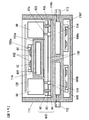
- FIG. 6 is a cross-sectional view taken along line AA in FIG. 5.
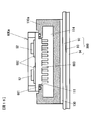
- FIG. 9 is a sectional view taken along line BB in FIG.
- FIG. 2 is an external perspective view of a power module 500.
- FIG. It is a perspective view which shows the direct current
- FIG. 5 is a diagram showing a case of single-sided cooling type power modules 600a to 600c mounted on cooling blocks 110a and 110b of the casing body 110.
- FIG. 5 is a diagram showing another example of single-sided cooling type power modules 600a to 600c. It is sectional drawing of the inverter apparatus provided with three cooling blocks 110a, 110g, and 110h.
- FIG. 1 is a diagram showing a control block of an electric vehicle (hereinafter referred to as “EV”) on which the inverter device of the present embodiment is mounted.
- the motor generator 20 not only generates a running torque for the vehicle, but also has a function of converting mechanical energy applied from the outside to the motor generator 20 into electric power.
- the motor generator 20 is, for example, a permanent magnet synchronous motor, and operates as a motor or a generator depending on the operation method.
- Rotational torque generated by the motor generator 20 is transmitted to the wheels 12 via the transmission 18 and the differential gear 16.
- rotational torque is transmitted from the wheels 12 to the motor generator 20, and AC power corresponding to the supplied rotational torque is generated.
- the generated AC power is converted into DC power by the inverter device 40, charges the high-voltage battery 30, and the charged power is used again as travel energy.
- the inverter device 40 is electrically connected to the battery 30 via the DC cable 32, and power is exchanged between the battery 30 and the inverter circuit 42.
- the motor generator 20 When the motor generator 20 is operated as a motor, the inverter device 40 generates AC power based on the DC power supplied from the battery 30 via the DC cable 32 and supplies the AC power to the motor generator 20 via the AC cable 34. .
- an insulated gate bipolar transistor is used as a semiconductor element, and hereinafter abbreviated as IGBT.
- An IGBT 52 and a diode 56 that operate as an upper arm, and an IGBT 62 and a diode 66 that operate as a lower arm constitute a series circuit 50 of upper and lower arms.
- the inverter circuit 42 includes the series circuit 50 corresponding to three phases of the U phase, the V phase, and the W phase of the AC power to be output.
- the three-phase series circuit 50 of the upper and lower arms outputs an alternating current from the intermediate electrode 69 of the series circuit.
- the intermediate electrode 69 is connected to an AC bus bar 86 via an AC terminal 59 and further electrically connected to each phase winding of the motor generator 20 via an AC connector 88.
- the collector electrode of the IGBT 52 of the upper arm is electrically connected to the positive electrode conductor plate 92 via the positive electrode terminal 57
- the emitter electrode of the IGBT 62 of the lower arm is electrically connected to the negative electrode conductor plate 94 via the negative electrode terminal 58.
- the positive electrode conductor plate 92 and the negative electrode conductor plate 94 are electrically connected to the capacitor 90, and are further electrically connected to the battery 30 via the DC connector 38.
- the control circuit 72 receives a control command from a host control device (not shown), and generates a control pulse for controlling the IGBTs 52 and 62 of the upper and lower arms constituting each series circuit 50 of the inverter circuit 42 based on the control command. , And supplies it to the driver circuit 74 as a control signal.
- the driver circuit 74 supplies a drive pulse for controlling the IGBTs 52 and 62 of each phase to the IGBT 52 via the signal emitter terminal 55 and the gate terminal 54 based on the control pulse, and the signal emitter terminal 65 and the gate. It is supplied to the IGBT 62 through the terminal 64.
- the IGBTs 52 and 62 of each phase perform conduction or cutoff operation based on the drive pulse from the driver circuit 74, convert the DC power supplied from the battery 30 into three-phase AC power, and supply it to the motor generator 20.
- the control circuit 72 includes a microcomputer (hereinafter referred to as “microcomputer”) for calculating the switching timing of the IGBTs 52 and 62.
- Information input to the microcomputer includes a target torque value required for the motor generator 20, a current value supplied from the series circuit 50 to the motor generator 20, and a magnetic pole position of the rotor of the motor generator 20.
- the target torque value is based on a command signal output from a host controller (not shown).
- the current value is detected based on a detection signal from the current sensor 80.
- the magnetic pole position is detected based on a detection signal output from a rotating magnetic pole sensor (not shown) such as a resolver provided in the motor generator 20.
- the microcomputer in the control circuit 72 calculates current command values for the d-axis and q-axis of the motor generator 20 based on the target torque value, and the calculated d-axis and q-axis current command values and the detected d-axis.
- the voltage command values for the d-axis and the q-axis are calculated based on the difference between the current values of the axes and the q-axis, and the calculated voltage command values for the d-axis and the q-axis are calculated based on the detected magnetic pole position. It is converted into voltage command values for phase, V phase, and W phase.
- the microcomputer generates a pulse-like modulated wave based on a comparison between the fundamental wave (sine wave) and the carrier wave (triangular wave) based on the voltage command values of the U phase, V phase, and W phase, and the generated modulation wave
- the wave is output to the driver circuit 74 as a PWM (pulse width modulation) signal.
- the driver circuit 74 When driving the lower arm, the driver circuit 74 outputs a drive signal obtained by amplifying the PWM signal to the gate electrode of the corresponding IGBT 62 of the lower arm. Further, when driving the upper arm, the driver circuit 74 amplifies the PWM signal after shifting the level of the reference potential of the PWM signal to the level of the reference potential of the upper arm, and uses this as a drive signal as a corresponding upper arm. Are output to the gate electrodes of the IGBTs 52 respectively.
- FIGS. 3 and 4 are external perspective views of the inverter device 40.
- FIG. FIG. 5 is a diagram in which the lid 117 is removed from the inverter device 40 shown in FIG. 3.
- FIG. 6 is a diagram showing a state in which the control board 120 is removed from FIG.
- FIG. 7 is an exploded perspective view of FIG.
- FIG. 8 is a cross-sectional view taken along the line AA in FIG. 9 is a cross-sectional view taken along the line BB of FIG.
- FIG. 10 is an external perspective view of the power module 500.
- FIG. 11 is a perspective view showing a DC bus bar 900 on which a capacitor 90 is mounted.
- FIG. 3 is an external perspective view of the inverter device 40 as viewed from the front side.
- FIG. 4 is an external perspective view of the inverter device 40 viewed from the back side.
- Electronic components constituting the inverter device 40 are accommodated in a casing formed by the casing main body 110 and the lid 117.
- the casing main body 110 is formed with a refrigerant flow path 114 to be described later.
- a refrigerant inlet 112 for taking in the refrigerant into the refrigerant flow path 114 and a refrigerant outlet for discharging the refrigerant. 113 is provided.
- a DC connector 38 is provided on the back side of the housing body 110.
- an AC connector 88 is provided on the front side of the lid 117, and a signal connector 76 is provided on the upper surface side of the lid 117.
- the signal connector 76 is provided for exchanging signals between the above-described control circuit 72 and the host control device, and is connected to a control board 120 described later.
- power module 500b, 500c, DC bus bar 900 on which capacitor 90 is mounted, power module 500a, and control board 120 are arranged in the housing body 110 in this order from the bottom of the housing.
- AC bus bars 86a to 86c are arranged on the front side of the housing with respect to the power modules 500a to 500c.
- FIG. 10 is an external perspective view of the power module 500.
- the power modules 500a to 500c have the same structure and are denoted by reference numeral 500 in FIG.
- the power modules 500a to 500c include power semiconductor elements (IGBT 52, IGBT 62, diode 56, diode 66) constituting the series circuit 50 of the upper and lower arms shown in FIG. 1 in a metallic module case 501 having heat radiation portions 502a and 502b. Is sealed.
- the power module 500a incorporates a series circuit 50 of U-phase upper and lower arms
- the power module 500b incorporates a series circuit 50 of V-phase upper and lower arms
- the power module 500c includes a series circuit 50 of W-phase upper and lower arms. Is built-in.
- the control signal connection terminal 70 is connected to the upper arm gate terminal 54, the upper arm emitter terminal 55, the lower arm gate terminal 64, and the lower arm emitter terminal 65 shown in FIG.
- the housing main body 110 is integrally formed with cooling blocks 110a and 110b in which a coolant channel 114 is formed.
- the cooling blocks 110a and 110b are arranged side by side with an interval in the vertical direction.
- One opening is formed in the coolant channel 114 of the upper cooling block 110a, and the power module 500a is attached to the opening.
- the cooling block 110b provided on the lower side two openings of the refrigerant flow path 114 are formed in the horizontal direction in the figure.
- the power module 500b is attached to the left opening, and the power module 500c is attached to the right opening.
- the power modules 500a to 500c are inserted into the refrigerant flow paths 114 of the cooling blocks 110a and 110b, the power modules 500b and 500c are arranged so that the AC terminal 59 comes to the center side of the cooling block 110b in FIGS. Inserted. By doing so, the AC terminals 59 are arranged close to each other, and the AC bus bars 86a to 86c connected to them can be arranged in one place.
- cooling block 110b may be divided into two cooling blocks 110g and 110h in which the refrigerant flow path 114 is formed.
- the flange portions 501a of the power modules 500a to 500c are fixed to the openings of the cooling blocks 110a and 110b, the portions of the module case 501 where the heat radiating portions 502a and 502b are provided are located in the refrigerant flow path 114 as shown in FIG. And the opening of the coolant channel 114 is sealed by the flange portion 501a.
- the flange portion 501a is fixed to the cooling blocks 110a and 110b with bolts or the like.
- the refrigerant that has flowed in from the refrigerant inlet 112 flows through the refrigerant flow path 114 as indicated by an arrow, and is discharged from the refrigerant outlet 113. That is, the refrigerant flowing in from the refrigerant inlet 112 flows into the refrigerant flow path 114 in which the power module 500b of the cooling block 110b is accommodated via the water channel connecting portion 115a. Thereafter, the refrigerant flows into the refrigerant flow path 114 in which the power module 500a of the cooling block 110a is accommodated via the water channel connecting portion 115b.
- the refrigerant flows into the refrigerant flow path 114 in which the power module 500c of the cooling block 110b is accommodated via the water channel connecting portion 115c. And the refrigerant
- coolant is discharged
- heat generated in the power semiconductor element is mainly radiated from the heat radiation surfaces 502a and 502b of the power module 500 to the refrigerant flowing through the refrigerant flow path 114.
- heat radiation surfaces 502a and 502b may be formed with columnar or plate-shaped heat radiation fins.
- a DC bus bar 900 on which a plurality of capacitors 90 are mounted is disposed.
- the DC bus bar 900 is a laminated bus bar in which a positive electrode conductor plate 92 and a negative electrode conductor plate 94 are laminated via a sheet-like insulating member 93 (insulating paper or resin).
- the positive electrode conductor plate 92 and the negative electrode conductor plate 94 are made of wide plate-like conductors.
- the capacitors 90 are distributed and arranged at positions symmetrical to the center of the DC bus bar 900, the balance of electrical characteristics (wiring inductance) is good.
- the positive electrode conductor plate 92 is formed with a positive electrode terminal portion 920 connected to the positive electrode terminal 57 of the power modules 500a to 500c.
- the negative conductor plate 94 is formed with a negative terminal portion 940 that is connected to the negative terminals 58 of the power modules 500a to 500c. Three sets of the positive electrode terminal portion 920 and the negative electrode terminal portion 940 are formed corresponding to the three power modules 500a to 500c.
- Each capacitor 90 is disposed on the positive electrode conductor plate 92 side of the DC bus bar 900, and a positive electrode terminal 91 a of each capacitor 90 is connected to the positive electrode conductor plate 92.
- the negative electrode terminal 91 b of each capacitor 90 passes through a through hole 921 formed in the positive electrode conductor plate 92 and is connected to the negative electrode conductor plate 94 on the opposite side.
- the positive electrode terminal 91 a connected to the positive electrode conductor plate 92 can be seen from the through hole 941 formed in the negative electrode conductor plate 94 of the DC bus bar 900.
- the positive electrode conductor plate 92 of the DC bus bar 900 disposed in the gap space 110c is in close contact with the wall surface of the cooling block 110a via the insulating sheet 130.
- the negative electrode conductor plate 94 of the DC bus bar 900 is in close contact with the wall surface of the cooling block 110b via the insulating sheet 130. That is, the DC bus bar 900 is in thermal contact with the wall surfaces of the cooling blocks 110a and 110b through which the refrigerant flows, and Joule heat generated in the DC bus bar 900 dissipates heat to the refrigerant flowing through the refrigerant flow path 114 via the cooling block wall surfaces. Is done. As a result, the DC bus bar 900 can be efficiently cooled.
- FIG. 6 shows the power modules 500a to 500c, the DC bus bar 900, and the plurality of capacitors 90 arranged in the housing main body 110.
- the plurality of capacitors 90 mounted on the DC bus bar 900 are arranged at both ends in the longitudinal direction of the DC bus bar 900. For this reason, when the DC bus bar 900 is inserted into the gap space 110c, the capacitors 90 arranged in the gap space 110c are arranged in empty spaces on both sides of the cooling block 110a.
- the DC bus bar 900 on which the capacitor 90 is mounted has a structure that is in thermal contact with the wall surfaces of the cooling blocks 110a and 110b, and is adjacent to the wall surfaces of the cooling blocks 110a and 110b through which the refrigerant flows. By arranging this, the temperature rise of the capacitor 90 can be suppressed. Further, by arranging the cooling block 110a so as to sandwich the cooling block 110a, the space between the cooling block 110a and the side wall of the casing body 110 can be used effectively, and the casing body 110 can be downsized.
- connection portion 6 is a connection portion between the power modules 500a to 500c and the DC bus bar 900.
- the negative terminals 58 of 500a to 500c are connected.
- control board 120 is disposed above the cooling block 110a and the capacitor 90, and the control signal connection terminals 70 of the power modules 500a to 500c are connected to the control board 120.
- Electronic components constituting the control circuit 72 and the driver circuit 74 are mounted on the control board 120.
- the control signal connection terminal 70 is pulled out from the module case 501 in the front direction of the housing, and then bent upward to the housing where the control board 120 is disposed. 6 and 10, the portion bent upward of the control signal connection terminal 70 is omitted.
- Embodiment- 12 to 13 are diagrams for explaining a second embodiment of the inverter device according to the present invention.
- the inverter device of the present embodiment is applied to a mechanical / electrical integrated rotating electrical machine.
- the casing main body 110 of the inverter device 40 is directly attached to the upper portion of the motor housing 200 provided with the motor stator 205 and the motor rotor 206.
- FIG. 13 is a perspective view of the inverter device 40 and corresponds to FIG. 5 of the first embodiment.
- the difference between the present embodiment and the first embodiment described above is the shape of the AC bus bars 86a to 86c, and the other configurations are the same as those of the first embodiment.
- An opening 110 e is formed on the bottom surface of the housing body 110.
- the AC bus bars 86a to 86c extend from the connection portions with the power modules 500a to 500c in the direction of the bottom of the housing, and project outside the housing through the opening 110e.
- AC bus bar 86a is connected to connection terminal 210a of the U-phase armature winding.
- AC bus bar 86b is connected to connection terminal 210b of the V-phase armature winding, and AC bus bar 86c is connected to connection terminal 210c of the W-phase armature winding.
- FIG. 14 is a diagram showing the arrangement of the control board 120.
- the AC bus bars 86a to 86c are configured to be drawn out of the housing from the bottom surface of the housing, so that the control board 120 can be disposed between the power modules 500a to 500c and the front side of the lid 117.
- the wiring for electrically connecting the control signal connection terminal 70 and the control board 120 of each module can be shortened and the noise of the control signal can be suppressed. Can be prevented.
- the AC bus bars 86a to 86c are taken out from the bottom surface of the casing fixed to the motor housing, thereby shortening the AC bus bar and the three-phase armature winding of the motor generator. It is possible to connect at a distance, and it is possible to reduce Joule loss generated in the connection cable.
- the power semiconductor elements (IGBT 52, IGBT 62, diode 56, diode 66) constituting the series circuit 50 of the upper and lower arms are made of a metal module having the heat radiation portions 502a and 502b.
- the module 501 is sealed in the case 501 and the module case 501 is arranged in the refrigerant flow path 114.
- the present invention can be applied not only to such a double-sided cooling type power module but also to single-sided cooling type power modules 600a to 600c as shown in FIGS.
- FIG. 15 is a diagram showing the case of single-sided cooling type power modules 600a to 600c mounted on the cooling blocks 110a and 110b of the casing body 110.
- FIG. 15 In the case of the housing body 110 shown in FIG. 15, a storage space 110f is also formed below the cooling block 110b.
- an insulating substrate 602 having a wiring pattern formed on a metal base 601 is provided, and the semiconductor power element described above is mounted on the insulating substrate 602.
- the power modules 600a to 600c are fixed so as to be in close contact with the outer wall surfaces of the cooling blocks 110a and 110b, respectively.
- FIG. 16 is a modification of the inverter device shown in FIG.
- FIG. 16 is an enlarged view of the power module 600a attached to the cooling block 110a.
- a plurality of heat radiation fins 603 are formed on the bottom surface side of the metal base 601.
- An opening 111 is formed on the mounting surface (upper surface in the drawing) of the cooling block 110a.
- the power module 600 a is attached to the cooling block 110 a so that the opening 111 is closed by the metal base 601.
- the heat radiation fin 603 is inserted into the refrigerant flow path 114.
- the heat radiation effect can be improved as compared with the structure shown in FIG.
- the inverter device of the above-described embodiment can achieve the following operational effects.
- the positive electrode conductor plate 92 and the negative electrode conductor plate 94 for supplying a direct current to the three power modules 500a to 500c form a plate-shaped laminated DC bus bar 900.
- the casing body 110 that functions as a cooling casing is provided with cooling blocks 110g and 110h in which a refrigerant flow path 114 is formed. Furthermore, the cooling blocks 110g and 110h are juxtaposed in the horizontal direction in the figure in the housing body 110, and the cooling block 110a is disposed with a gap with respect to the juxtaposed cooling blocks 110g and 110h.
- one surface (the surface of the positive electrode conductor plate 92) is in thermal contact with the cooling block 110a, and the other surface (the surface of the negative electrode conductor plate 94) is thermally connected to the cooling blocks 110g and 110h. Is arranged in a gap space 110c (see FIG. 9) between the cooling block 110a and the cooling blocks 110g and 110h.
- the DC bus bar 900 since the DC bus bar 900 is brought into thermal contact with the cooling blocks 110a, 110g, 110h through which the refrigerant flows, the DC bus bar 900 can be cooled from both sides, and Joule heat generated in the DC bus bar 900 can be reduced. It is possible to efficiently dissipate heat to the refrigerant. Further, by laminating the positive electrode conductor plate 92 and the negative electrode conductor plate 94 constituting the DC bus bar 900, the wiring inductance can be reduced. Furthermore, by arranging the cooling blocks 110a, 110g, and 110h on the front and back sides of the plate-shaped stacked DC bus bar 900, the housing body 110 can be downsized.
- the cooling block disposed on the negative electrode conductor plate 94 side is provided for each of the power modules 500b and 500c.
- the two cooling blocks 110g and 110h are integrated into the integrated cooling block 110b. You can put it together. That is, the cooling block 110b corresponds to the second and third cooling blocks.
- the present invention can be similarly applied to a single-sided cooling type power module in which a power semiconductor element is provided on a metal base 601, and similar operational effects can be achieved.
- the power modules 500b and 500c are disposed in the refrigerant flow path 114 of the cooling block 110b that constitutes the second and third cooling blocks, and in the refrigerant flow path 114 of the cooling block 110a.
- the power module 500a is arranged, and the cooling block 110a is arranged in parallel so as to face the middle of the cooling block 110b.
- a plurality of capacitors 90 in which the positive electrode terminal 91 a is connected to the positive electrode conductor plate 92 and the negative electrode terminal 91 b is connected to the negative electrode conductor plate 94 are connected to the positive electrode conductor plate 92 side of the laminated DC bus bar 900. Further, by arranging the cooling block 110a so as to sandwich the cooling block 110a, the space between the cooling block 110a and the side wall of the casing body 110 can be used effectively, and the casing body 110 can be downsized.
- an insulating resin eg, polyethylene terephthalate
- the insulating sheet formed by the above the adhesion between the laminated DC bus bar 900 and the block wall surface is improved.
- the insulating resin may be poured into the gap after the DC bus bar 900 is inserted into the gap space 110c.
- the power modules 500a to 500b are inserted in parallel to the bottom surface of the casing with respect to the refrigerant flow paths 114 of the cooling blocks 110a and 110b, so that each AC terminal 59 is connected to the front of the casing. Align to the side. Therefore, as shown in FIG. 12, when the inverter device 40 is used as an inverter device of an electromechanical integrated rotary machine in which the bottom surface of the housing body 110 is integrally fixed to the motor housing 200, the AC bus bars 86a to 86c are It becomes possible to easily connect to the connection terminals 210a to 210c of the armature winding through the opening 110e formed on the bottom surface of the housing. Further, with such a configuration, the length of the AC bus bars 86a to 86c can be shortened.
- the refrigerant flowing in from the refrigerant inlet 112 flows into the cooling block 110g, the cooling block 110a, and the cooling block 110h arranged in this order from the refrigerant inlet 112 along the refrigerant outlet 113. Then, the refrigerant is discharged from the refrigerant outlet 113. Therefore, the length of the refrigerant flow path is shortened, the pressure loss can be suppressed, and effective cooling can be performed.
- Various refrigerants including cooling water can be used as the refrigerant.
Landscapes
- Engineering & Computer Science (AREA)
- Microelectronics & Electronic Packaging (AREA)
- Power Engineering (AREA)
- Physics & Mathematics (AREA)
- Thermal Sciences (AREA)
- Inverter Devices (AREA)
Abstract
直流バスバーが効果的に冷却されるとともに、小型化を図ることができるインバータ装置を提供するために、インバータ装置において、3つのパワーモジュール500a~500cに直流電流を供給するための正極導体板92および負極導体板94は、板状の積層型直流バスバー900を形成している。筐体本体110には、冷媒流路114が形成された冷却ブロック110g,110hが設けられている。さらに、冷却ブロック110g,110hは筐体本体110内に並設され、冷却ブロック110aは、並設された冷却ブロック110g,110hに対して隙間を介して配設されている。積層型直流バスバー900は、一方の面(正極導体板92の面)が冷却ブロック110aに熱的に接触するとともに、他方の面(負極導体板94の面)が冷却ブロック110g,110hに熱的に接触するように、冷却ブロック110aと冷却ブロック110g,110hとの隙間空間110cに配設されている。
Description
本発明は、インバータ回路を備えたインバータ装置、特に、電気自動車およびハイブリッド自動車に搭載される車載用のインバータ装置に関する。
電気自動車あるいはハイブリッド自動車においては、車両の動力源としてモータを搭載しており、一般的にモータに供給する電力を制御するためにインバータ装置を備えている。インバータ装置は、IGBTなどの電力用半導体素子を内蔵したパワーモジュール、そのパワーモジュールを駆動する駆動回路、それらを制御する制御回路、バッテリから供給される電力の配線である直流バスバー、モータへ供給する電力の配線である交流バスバー、および電流平滑化用のコンデンサを備えている。
ところで、電力用半導体素子は発熱が大きく、一般的に、素子温度が動作保証温度以下に保持されるように冷却装置が設けられている(例えば、特許文献1参照)。特許文献1に記載の発明では、冷媒が流れる冷却装置に、電力用半導体素子が設けられたパワー部品を搭載し、正極バスバーと負極バスバーを個別に絶縁樹脂から成るブロック部内に埋設するようにしている。このようにすることで、半導体素子と正極バスバーおよび負極バスバーとを冷却するようにしている。
しかしながら、上述した従来のインバータ装置では、パワー部品が平面的に搭載されるとともに、正極バスバーおよび負極バスバーがブロック部の異なる領域に個別に設けられているため、インバータ装置が大型化しやすいという問題があった。
請求項1の発明に係るインバータ装置は、直流電力を三相交流電力に変換するインバータ回路の第1の相を構成する半導体素子が設けられた第1のパワーモジュールと、インバータ回路の第2の相を構成する半導体素子が設けられた第2のパワーモジュールと、インバータ回路の第3の相を構成する半導体素子が設けられた第3のパワーモジュールと、第1、第2および第3のパワーモジュールに直流電流を供給するための正極バスバーおよび負極バスバーが積層された、板状の積層型直流バスバーと、第1、第2および第3のパワーモジュールに各々接続されて、各相の交流電流を出力する第1、第2および第3の交流バスバーと、第1、第2および第3のパワーモジュール、積層型直流バスバー、第1、第2および第3の交流バスバーが収納されるとともに、冷媒流路が形成され第1のパワーモジュールを冷却する第1冷却ブロック、冷媒流路が形成され前記第2のパワーモジュールを冷却する第2冷却ブロック、および冷媒流路が形成され第3のパワーモジュールを冷却する第3冷却ブロックを有する冷却筐体と、を備え、第2冷却ブロックおよび第3冷却ブロックは冷却筐体内に並設され、第1冷却ブロックは、並設された第2および第3冷却ブロックに対して隙間を介して配設され、積層型直流バスバーは、該直流バスバーの一方の面が第1冷却ブロックに熱的に接触するとともに他方の面が第2および第3冷却ブロックに熱的に接触するように、隙間に配設されていることを特徴とする。
本発明によれば、直流バスバーが効果的に冷却されるとともに、インバータ装置の小型化を図ることができる。
以下、図を参照して本発明を実施するための形態について説明する。
-第1の実施の形態-
図1は、本実施の形態のインバータ装置が搭載された電気自動車(以下「EV」と記述する)の制御ブロックを示す図である。モータジェネレータ20は車両の走行用トルクを発生するだけでなく、モータジェネレータ20に外部から加えられる機械エネルギーを電力に変換する機能を有する。 モータジェネレータ20は、例えば永久磁石同期電動機であり、運転方法によりモータとしても発電機としても動作する。
-第1の実施の形態-
図1は、本実施の形態のインバータ装置が搭載された電気自動車(以下「EV」と記述する)の制御ブロックを示す図である。モータジェネレータ20は車両の走行用トルクを発生するだけでなく、モータジェネレータ20に外部から加えられる機械エネルギーを電力に変換する機能を有する。 モータジェネレータ20は、例えば永久磁石同期電動機であり、運転方法によりモータとしても発電機としても動作する。
モータジェネレータ20が発生する回転トルクは、変速機18およびデファレンシャルギア16を介して車輪12に伝達される。一方、回生制動の運転時には、車輪12から回転トルクがモータジェネレータ20に伝達され、供給されてきた回転トルクに応じた交流電力を発生する。発生した交流電力はインバータ装置40により直流電力に変換され、高電圧用のバッテリ30を充電し、充電された電力は再び走行エネルギーとして使用される。
インバータ装置40は、バッテリ30と直流ケーブル32を介して電気的に接続されており、バッテリ30とインバータ回路42との相互において電力の授受が行われる。モータジェネレータ20をモータとして動作させる場合には、インバータ装置40は直流ケーブル32を介してバッテリ30から供給された直流電力に基づき交流電力を発生し、交流ケーブル34を介してモータジェネレータ20に供給する。
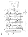
次に、図2を用いてインバータ回路42の電気回路の構成を説明する。なお、以下で半導体素子として絶縁ゲート型バイポーラトランジスタを使用しており、以下略してIGBTと記す。上アームとして動作するIGBT52及びダイオード56と、下アームとして動作するIGBT62及びダイオード66とで、上下アームの直列回路50が構成される。インバータ回路42は、この直列回路50を、出力しようとする交流電力のU相,V相,W相の三相に対応して備えている。
これらの三相は、この実施の形態ではモータジェネレータ20の電機子巻線の三相の各相巻線に対応している。三相のそれぞれの上下アームの直列回路50は、直列回路の中間電極69から交流電流を出力する。この中間電極69は、交流端子59を介して、交流バスバー86と接続され、さらに交流コネクタ88を介して、モータジェネレータ20の各相巻線に電気的に接続されている。
上アームのIGBT52のコレクタ電極は、正極端子57を介して正極導体板92に、また、下アームのIGBT62のエミッタ電極は、負極端子58を介して負極導体板94に電気的に接続されている。正極導体板92および負極導体板94はコンデンサ90に電気的に接続されており、さらに直流コネクタ38を介して、バッテリ30に電気的に接続されている。制御回路72は、上位の制御装置(不図示)から制御指令を受け、これに基づいてインバータ回路42の各直列回路50を構成する上下アームのIGBT52,62を制御するための制御パルスを発生し、それを制御信号としてドライバ回路74に供給する。
ドライバ回路74は、上記制御パルスに基づき、各相のIGBT52,62を制御するための駆動パルスを、信号用エミッタ端子55およびゲート端子54を介してIGBT52に供給し、信号用エミッタ端子65およびゲート端子64を介してIGBT62に供給する。各相のIGBT52,62は、ドライバ回路74からの駆動パルスに基づいて導通あるいは遮断動作を行い、バッテリ30から供給された直流電力を三相交流電力に変換し、モータジェネレータ20に供給する。
制御回路72は、IGBT52,62のスイッチングタイミングを演算処理するためのマイクロコンピュータ(以下、「マイコン」と記述する)を備えている。マイコンへの入力情報としては、モータジェネレータ20に対して要求される目標トルク値、直列回路50からモータジェネレータ20に供給される電流値、及びモータジェネレータ20の回転子の磁極位置がある。目標トルク値は、不図示の上位制御装置から出力された指令信号に基づくものである。電流値は、電流センサ80による検出信号に基づいて検出されたものである。磁極位置は、モータジェネレータ20に設けられたレゾルバなどの回転磁極センサ(不図示)から出力された検出信号に基づいて検出されたものである。
制御回路72内のマイコンは、目標トルク値に基づいてモータジェネレータ20のd軸、q軸の電流指令値を演算し、この演算されたd軸、q軸の電流指令値と、検出されたd軸、q軸の電流値との差分に基づいてd軸、q軸の電圧指令値を演算し、この演算されたd軸、q軸の電圧指令値を、検出された磁極位置に基づいてU相、V相、W相の電圧指令値に変換する。そして、マイコンは、U相、V相、W相の電圧指令値に基づく基本波(正弦波)と搬送波(三角波)との比較に基づいてパルス状の変調波を生成し、この生成された変調波をPWM(パルス幅変調)信号としてドライバ回路74に出力する。
ドライバ回路74は、下アームを駆動する場合、PWM信号を増幅したドライブ信号を、対応する下アームのIGBT62のゲート電極に出力する。また、ドライバ回路74は、上アームを駆動する場合、PWM信号の基準電位のレベルを上アームの基準電位のレベルにシフトしてからPWM信号を増幅し、これをドライブ信号として、対応する上アームのIGBT52のゲート電極にそれぞれ出力する。
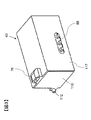
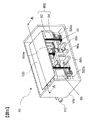
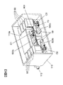
次に、図3~11を用いてインバータ装置40の構成について説明する。図3および図4は、インバータ装置40の外観斜視図である。図5は、図3に示すインバータ装置40から蓋117を取り外した図である。図6は、図5において制御基板120を取り除いた状態を示す図である。図7は、図6の分解斜視図である。図8は、図5のA-A断面図である。図9は、図8のB-B断面図である。図10は、パワーモジュール500の外観斜視図である。図11は、コンデンサ90が搭載された直流バスバー900を示す斜視図である。
図3は、インバータ装置40を正面側から観た外観斜視図である。一方、図4は、インバータ装置40を背面側から観た外観斜視図である。インバータ装置40を構成する電子部品は、筐体本体110と蓋117とで形成されるケーシング内に収納されている。筐体本体110には後述する冷媒流路114が形成されており、図4に示すように、冷媒流路114に冷媒を取り入れるための冷媒流入口112と、冷媒を排出するための冷媒流出口113とが設けられている。筐体本体110の背面側には、直流コネクタ38が設けられている。
一方、蓋117の正面側には交流コネクタ88が設けられ、蓋117の上面側には信号用コネクタ76が設けられている。信号用コネクタ76は、上述した制御回路72と上位の制御装置との間で信号を授受するために設けられたものであり、後述する制御基板120に接続されている。
図5に示すように、筐体本体110内には、筐体底部から順に、パワーモジュール500b,500c、コンデンサ90が搭載された直流バスバー900、パワーモジュール500a、制御基板120が配置されている。パワーモジュール500a~500cに対して筐体正面側には、交流バスバー86a~86cが配置されている。
図10は、パワーモジュール500の外観斜視図である。なお、パワーモジュール500a~500cは同一構造を有しており、図10では符号500を付した。パワーモジュール500a~500cは、図1に示した上下アームの直列回路50を構成するパワー半導体素子(IGBT52、IGBT62、ダイオード56、ダイオード66)を放熱部502a,502bを有する金属性のモジュールケース501内に封止したものである。パワーモジュール500aにはU相の上下アームの直列回路50が内蔵され、パワーモジュール500bにはV相の上下アームの直列回路50が内蔵され、パワーモジュール500cにはW相の上下アームの直列回路50が内蔵されている。
モジュールケース501のフランジ部501aには開口が形成されており、正極端子57、負極端子58、交流端子59および制御信号用接続端子70が開口から外部に突出している。制御信号用接続端子70には、図2に示した上アームゲート端子54、上アームエミッタ端子55、下アームゲート端子64、下アームエミッタ端子65が接続されている。
図7~9に示すように、筐体本体110には、冷媒流路114が形成された冷却ブロック110a,110bが一体に形成されている。冷却ブロック110a,110bは上下に間隔を開けて並設されている。上側の冷却ブロック110aの冷媒流路114には開口部が1箇所形成されており、その開口部にパワーモジュール500aが装着される。一方、下側に設けられた冷却ブロック110bには、冷媒流路114の開口部が図示左右方向に2箇所形成されている。左側の開口部にパワーモジュール500bが装着され、右側の開口部にパワーモジュール500cが装着される。
パワーモジュール500a~500cを冷却ブロック110a,110bの冷媒流路114内に挿入する際、パワーモジュール500b,500cは、図6,7に交流端子59が冷却ブロック110bの中央側に来るような配置で挿入される。そうすることで、各交流端子59が近接して配置され、それらに接続される交流バスバー86a~86cを一箇所に纏めて配置することができる。
なお、図9に示す例では、一つの冷却ブロック110bに2つの冷媒流路114を図示左右方向に配置する構成とした。しかし、図17に示すように、冷却ブロック110bを、冷媒流路114が形成された2つの冷却ブロック110g,110hに分割するようにしても良い。
パワーモジュール500a~500cのフランジ部501aを冷却ブロック110a,110bの各開口部に固定すると、図9に示すように、モジュールケース501の放熱部502a,502bが設けられた部分が冷媒流路114内に収納され、冷媒流路114の開口部がフランジ部501aによって封止される。なお、図示は省略したが、フランジ部501aはボルト等によって冷却ブロック110a,110bに固定される。
図4に示すように、冷媒流入口112から流入した冷媒は、矢印で示すように冷媒流路114内を流れて、冷媒流出口113から排出される。すなわち、冷媒流入口112から流入した冷媒は、水路接続部115aを介して、冷却ブロック110bのパワーモジュール500bが収納されている冷媒流路114に流入する。その後、冷媒は、水路接続部115bを介して、冷却ブロック110aのパワーモジュール500aが収納されている冷媒流路114に流入する。その後、冷媒は、水路接続部115cを介して、冷却ブロック110bのパワーモジュール500cが収納されている冷媒流路114に流入する。そして、その冷媒は、水路接続部115cを介して冷媒流出口113から排出される。
パワー半導体素子で発生する熱は、主としてパワーモジュール500の放熱面502a,502bから冷媒流路114を流れる冷媒に放熱される。なお、放熱面502a、502bには、冷媒との接触面積を大きくするため、柱状、あるいは板状の放熱フィンが形成されていても良い。
冷却ブロック110aと冷却ブロック110bとの間に形成された隙間空間110c(図9参照)には、複数のコンデンサ90が搭載された直流バスバー900が配置される。直流バスバー900は、正極導体板92と負極導体板94とをシート状の絶縁部材93(絶縁紙や樹脂)を介して積層したラミネートバスバーである。図11に示すように、正極導体板92および負極導体板94は幅広の板状導体から成る。このように面積の大きな正極導体板92および負極導体板94を積層構造とすることにより、直流バスバー900の抵抗値およびインダクタンスの低減を図ることができる。直流バスバー900の中央に対して対称な位置にコンデンサ90が振り分けで配置されているため、電気的な特性(配線インダクタンス)のバランスが良い。
正極導体板92には、パワーモジュール500a~500cの正極端子57と接続される正極端子部920が形成されている。負極導体板94には、パワーモジュール500a~500cの負極端子58と接続される負極端子部940が形成されている。正極端子部920および負極端子部940は、3つのパワーモジュール500a~500cに対応して3組形成されている。
各コンデンサ90は直流バスバー900の正極導体板92側に配置されており、各コンデンサ90の正極端子91aは正極導体板92に接続されている。一方、各コンデンサ90の負極端子91bは、正極導体板92に形成された貫通穴921を貫通して、反対側の負極導体板94に接続されている。図11に示すように、直流バスバー900の負極導体板94に形成された貫通穴941からは、正極導体板92に接続された正極端子91aが見えている。
隙間空間110cに配置された直流バスバー900の正極導体板92は、絶縁シート130を介して冷却ブロック110aの壁面と密着している。同様に、直流バスバー900の負極導体板94は、絶縁シート130を介して冷却ブロック110bの壁面と密着している。すなわち、直流バスバー900は冷媒が流れる冷却ブロック110a,110bの壁面と熱的に接触しており、直流バスバー900で発生したジュール熱は、冷却ブロック壁面を介して冷媒流路114を流れる冷媒に放熱される。その結果、直流バスバー900を効率良く冷却することができる。
図6は、筐体本体110内に配置された、パワーモジュール500a~500c、直流バスバー900および複数のコンデンサ90を示している。直流バスバー900に搭載されている複数のコンデンサ90は、直流バスバー900の長手方向両端に振り分けで配置されている。そのため、直流バスバー900を隙間空間110cに挿入すると、それぞれに配置されたコンデンサ90が、冷却ブロック110aの両側の空きスペースに配置されることになる。
上述したように、コンデンサ90が搭載されている直流バスバー900が冷却ブロック110a,110bの壁面と熱的に接触する構造とするとともに、冷媒が流れる冷却ブロック110a,110bの壁面に近接してコンデンサ90を配置することで、コンデンサ90の温度上昇を抑えることができる。また、冷却ブロック110aを挟むように配置したことにより、冷却ブロック110aと筐体本体110の側壁とのスペースを有効に利用することができ、筐体本体110の小型化を図ることができる。
図6の符号C1~C3で示す部分は、パワーモジュール500a~500cと直流バスバー900との接続部分である。各接続部分C1~C3においては、正極導体板92に形成された正極端子部920がパワーモジュール500a~500cの正極端子57と接続され、負極導体板94に形成された負極端子部940がパワーモジュール500a~500cの負極端子58と接続されている。
図6の状態に組み付けた後に、各パワーモジュール500a~500cの交流端子59に、対応する交流バスバー86a~86cを溶接等により接続する。また、冷却ブロック110aおよびコンデンサ90の上方に制御基板120を配置し、パワーモジュール500a~500cの各制御信号用接続端子70を制御基板120に接続する。制御基板120には、制御回路72およびドライバ回路74を構成する電子部品が実装されている。制御信号用接続端子70は、モジュールケース501から筐体正面方向に引き出された後に、制御基板120が配置される筐体上方へと折り曲げられている。なお、図6、10では、制御信号用接続端子70の上方に折り曲げられた部分は省略して示した。
-第2の実施の形態-
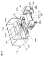
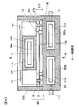
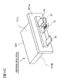
図12~13は、本発明によるインバータ装置の第2の実施形態を説明する図である。本実施形態のインバータ装置は、図12に示すように、機電一体型回転電機に適用されるものである。図12に示す機電一体型回転電機では、モータ固定子205およびモータ回転子206が設けられたモータハウジング200の上部に、インバータ装置40の筐体本体110が直接取り付けられる。
図12~13は、本発明によるインバータ装置の第2の実施形態を説明する図である。本実施形態のインバータ装置は、図12に示すように、機電一体型回転電機に適用されるものである。図12に示す機電一体型回転電機では、モータ固定子205およびモータ回転子206が設けられたモータハウジング200の上部に、インバータ装置40の筐体本体110が直接取り付けられる。
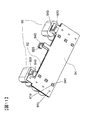
図13は、インバータ装置40の斜視図であり、第1の実施の形態の図5に対応する図である。本実施の形態と上述した第1の実施の形態との相違点は交流バスバー86a~86cの形状であり、その他の構成は、第1の実施の形態と同様の構成である。筐体本体110の底面には開口110eが形成されている。交流バスバー86a~86cは、パワーモジュール500a~500cとの接続部分から、筐体底面方向に伸延し、開口110eを貫通して筐体外部に突出している。
モータハウジング200の上部にも交流バスバー86a~86cを通すための貫通穴が形成されており、インバータ装置40をモータハウジング200の上部に固定すると、交流バスバー86a~86cはそれらの貫通穴を通ってハウジング内に導入される。そして、交流バスバー86aは、U相電機子巻線の接続端子210aに接続される。同様に、交流バスバー86bはV相電機子巻線の接続端子210bに接続され、交流バスバー86cはW相電機子巻線の接続端子210cに接続される。
図14は、制御基板120を配置を示す図である。本実施の形態では、交流バスバー86a~86cを筐体底面から筐体外に引き出す構成としているため、パワーモジュール500a~500cと蓋117の正面側との間に制御基板120を配置することができる。このような配置とすることにより、各モジュールの制御信号用接続端子70と制御基板120とを電気的に接続する配線が短くなり、制御信号のノイズを抑えることができるため、半導体素子の誤動作を防ぐことができる。
本実施の形態では、図12に示すように、モータハウジングに固定されている筐体底面から交流バスバー86a~86cを取り出すことで、交流バスバーとモータジェネレータの三相の電機子巻線とを短い距離で接続することが可能になるり、接続ケーブルで発生するジュール損失を低減することができる。
なお、上述した第1および第2の実施の形態では、上下アームの直列回路50を構成するパワー半導体素子(IGBT52、IGBT62、ダイオード56、ダイオード66)を放熱部502a,502bを有する金属性のモジュールケース501内に封止し、そのモジュールケース501を冷媒流路114内に配置するような構成とした。しかし、本発明は、このような両面冷却型のパワーモジュールに限らず、図15,16に示すような片面冷却型のパワーモジュール600a~600cにも適用できる。
図15は、筐体本体110の冷却ブロック110a,110bに装着された片面冷却型のパワーモジュール600a~600cを場合を示す図である。図15に示す筐体本体110の場合には、冷却ブロック110bの下側にも収納空間110fが形成されている。片面冷却型のパワーモジュール600a~600cにおいては、金属ベース601上に配線パターンが形成された絶縁基板602を設け、その絶縁基板602上に上述した半導体パワー素子が実装されている。パワーモジュール600a~600cは、それぞれ冷却ブロック110a,110bの外壁面に密着するように固定されている。
図16は、図15に示すインバータ装置の変形例である。図16は、冷却ブロック110aに装着されたパワーモジュール600aの拡大図である。金属ベース601の底面側には放熱フィン603が複数形成されている。冷却ブロック110aの装着面(図示上面)には開口111が形成されている。パワーモジュール600aは、金属ベース601により開口111が塞がれるように冷却ブロック110aに取り付けられる。その結果、放熱フィン603が冷媒流路114内に挿入される。このように、金属ベース601を冷媒により直接冷却することにより、図15に示す構造に比べて放熱効果を向上させることができる。
上述した実施の形態のインバータ装置は、以下のような作用効果を奏することができる。
(1)図17に示すインバータ装置は、3つのパワーモジュール500a~500cに直流電流を供給するための正極導体板92および負極導体板94は、板状の積層型直流バスバー900を形成している。また、冷却筐体として機能する筐体本体110には、冷媒流路114が形成された冷却ブロック110g,110hが設けられている。さらに、冷却ブロック110g,110hは筐体本体110内の図示左右方向に並設され、冷却ブロック110aは、並設された冷却ブロック110g,110hに対して隙間を介して配設されている。積層型直流バスバー900は、一方の面(正極導体板92の面)が冷却ブロック110aに熱的に接触するとともに、他方の面(負極導体板94の面)が冷却ブロック110g,110hに熱的に接触するように、冷却ブロック110aと冷却ブロック110g,110hとの隙間空間110c(図9参照)に配設されている。
(1)図17に示すインバータ装置は、3つのパワーモジュール500a~500cに直流電流を供給するための正極導体板92および負極導体板94は、板状の積層型直流バスバー900を形成している。また、冷却筐体として機能する筐体本体110には、冷媒流路114が形成された冷却ブロック110g,110hが設けられている。さらに、冷却ブロック110g,110hは筐体本体110内の図示左右方向に並設され、冷却ブロック110aは、並設された冷却ブロック110g,110hに対して隙間を介して配設されている。積層型直流バスバー900は、一方の面(正極導体板92の面)が冷却ブロック110aに熱的に接触するとともに、他方の面(負極導体板94の面)が冷却ブロック110g,110hに熱的に接触するように、冷却ブロック110aと冷却ブロック110g,110hとの隙間空間110c(図9参照)に配設されている。
このように、直流バスバー900を冷媒が流れる冷却ブロック110a,110g、110hに熱的に接触させるようにしたので、直流バスバー900を両面から冷却することができ、直流バスバー900で発生するジュール熱を冷媒へと効率的に放熱することができる。また、直流バスバー900を構成する正極導体板92および負極導体板94を積層することにより、配線インダクタンスの低減を図れる。さらに、板状の積層型直流バスバー900の表裏両面側に冷却ブロック110a,110g、110hを振り分けて配置することで、筐体本体110の小型化を図ることができる。
なお、図17では負極導体板94側に配置される冷却ブロックを、パワーモジュール500b,500c毎に設けたが、図8に示すように、2つの冷却ブロック110g,110hを一体の冷却ブロック110bにまとめても構わない。すなわち、冷却ブロック110bは第2および第3の冷却ブロックに対応している。また、図15,16に示すように、金属ベース601上にパワー半導体素子を設ける片面冷却型のパワーモジュールに対しても同様に適用でき、同様の作用効果を奏することができる。
(2)図7に示すように、第2および第3冷却ブロックを構成する冷却ブロック110bの冷媒流路114内にパワーモジュール500b,500cを配置するとともに、冷却ブロック110aの冷媒流路114内にパワーモジュール500aを配置し、さらに、冷却ブロック110aを冷却ブロック110bの中間と対向するように並設した。それにより、交流バスバー86aを交流バスバー86b、86cの間に位置するように設けることで、交流バスバーの長さを極力短くすることができる。その結果、ジュール損失を低減することができる。
(3)図8に示すように、正極端子91aが正極導体板92に接続され負極端子91bが負極導体板94に接続される複数のコンデンサ90を、積層型直流バスバー900の正極導体板92側に、冷却ブロック110aを挟むように配置したことにより、冷却ブロック110aと筐体本体110の側壁とのスペースを有効に利用することができ、筐体本体110の小型化を図ることができる。
(4)また、図8,9に示すように、積層型直流バスバー900を隙間空間110cに配置する場合に、直流バスバー900と冷却ブロックとの間に絶縁性樹脂(例えば、ポリエチレンテレフタラート等)により形成された絶縁シートを設けることにより、積層型直流バスバー900とブロック壁面との密着性が向上する。ここでは、シート状の樹脂としたが、隙間空間110cに直流バスバー900を挿入した後に、絶縁性樹脂を隙間に流し込むようにしても良い。
(5)図7に示すように冷却ブロック110a,110bの冷媒流路114に対して、パワーモジュール500a~500bを筐体底面に対して平行に挿入することで、各交流端子59が筐体正面側に揃う。そのため、図12に示すように、インバータ装置40を、筐体本体110の底面がモータハウジング200に一体に固定される機電一体型回転機のインバータ装置として用いる場合に、交流バスバー86a~86cを、筐体底面に形成された開口110eを通して電機子巻線の接続端子210a~210cに容易に接続することが可能となる。また、そのような構成とすることで、交流バスバー86a~86cの長さを短縮することができる。
(6)図17に示すように、冷媒流入口112から流入した冷媒は、冷媒流入口112から冷媒流出口113に沿って順に配置された冷却ブロック110g、冷却ブロック110a、冷却ブロック110hに順に流れ込み、冷媒流出口113から排出される。そのため、冷媒流路の長さが短縮されると共に、圧損を小さく抑えることができ、効果的な冷却を行うことができる。なお、冷媒には、冷却水を含め種々のものを用いることができる。
以上説明した実施の形態では、電気自動車の駆動用モータ、インバータを一体化したシステムについて言及しているが、ハイブリッド自動車への適用や、モータ、インバータを別々に構成したシステムへの適用も可能であり、上記実施形態の構成に限定されるものではない。また、上述した各実施形態はそれぞれ単独に、あるいは組み合わせて用いても良い。それぞれの実施形態での効果を単独あるいは相乗して奏することができるからである。
20:モータジェネレータ、30:バッテリ、40:インバータ装置、42:インバータ回路、50:直列回路、52,62:IGBT、56,66:ダイオード、86,86a~86c:交流バスバー、90:コンデンサ、92:正極導体板、93:絶縁部材、94:負極導体板、110:筐体本体、110a~110c,110g,110h:冷却ブロック、110e,111:開口、112:冷媒流入口、113:冷媒流出口、120:制御基板、130:絶縁シート、200:モータハウジング、210a~210c:接続端子、500,500a~500c,600,600a~600c:パワーモジュール、900:直流バスバー
Claims (6)
- 直流電力を三相交流電力に変換するインバータ回路の第1の相を構成する半導体素子が設けられた第1のパワーモジュールと、
前記インバータ回路の第2の相を構成する半導体素子が設けられた第2のパワーモジュールと、
前記インバータ回路の第3の相を構成する半導体素子が設けられた第3のパワーモジュールと、
前記第1、第2および第3のパワーモジュールに直流電流を供給するための正極バスバーおよび負極バスバーが積層された、板状の積層型直流バスバーと、
前記第1、第2および第3のパワーモジュールに各々接続されて、各相の交流電流を出力する第1、第2および第3の交流バスバーと、
前記第1、第2および第3のパワーモジュール、前記積層型直流バスバー、前記第1、第2および第3の交流バスバーが収納されるとともに、冷媒流路が形成され前記第1のパワーモジュールを冷却する第1冷却ブロック、冷媒流路が形成され前記第2のパワーモジュールを冷却する第2冷却ブロック、および冷媒流路が形成され前記第3のパワーモジュールを冷却する第3冷却ブロックを有する冷却筐体と、を備え、
前記第2冷却ブロックおよび第3冷却ブロックは前記冷却筐体内に並設され、
前記第1冷却ブロックは、前記並設された前記第2および第3冷却ブロックに対して隙間を介して配設され、
前記積層型直流バスバーは、該直流バスバーの一方の面が前記第1冷却ブロックに熱的に接触するとともに他方の面が前記第2および第3冷却ブロックに熱的に接触するように、前記隙間に配設されていることを特徴とするインバータ装置。 - 請求項1に記載のインバータ装置において、
前記第1、第2および第3のパワーモジュールは、それらに対応する前記第1、第2および第3冷却ブロックの冷媒流路内にそれぞれ配置され、
前記第2および第3冷却ブロックと隙間を介して並設される前記第1冷却ブロックは、前記第2冷却ブロックと前記第3冷却ブロックと間に対向するように並設され、
前記第1の交流バスバーが、前記第2および第3の交流バスバーの間に位置することを特徴とするインバータ装置。 - 請求項2に記載のインバータ装置において、
正極端子が前記正極バスバーに接続され負極端子が前記負極バスバーに接続される複数のコンデンサを、前記積層型直流バスバーの前記一方の面側に、前記第1冷却ブロックを挟むように配置したことを特徴とするインバータ装置。 - 請求項1乃至3のいずれか一項に記載のインバータ装置において、
前記正極バスバーおよび負極バスバーは、絶縁性の樹脂を介して前記冷却ブロックに熱的に接触していることを特徴とするインバータ装置。 - 請求項2または3に記載のインバータ装置において、
前記冷却筐体は、前記インバータ回路により駆動される回転電機のハウジングに固定される筐体底面に開口を有し、
前記冷媒流路内に配置される前記第1、第2および第3のパワーモジュールは、前記筐体底面に対して平行に挿入され、
前記第1、第2および第3の交流バスバーは、前記開口から筐体外へ引き出され、前記ハウジングに設けられた電機子巻線端子に接続されることを特徴とする機電一体型回転電機のインバータ装置。 - 請求項2または3に記載のインバータ装置において、
前記冷却筐体は、冷媒流入部および冷媒排出部を有し、
前記冷媒流入部から流入した冷媒は、前記第2冷却ブロック、前記第1冷却ブロック、前記第3冷却ブロックの順に流れ、その後、前記冷媒排出部から排出されることを特徴とするインバータ装置。
Applications Claiming Priority (2)
| Application Number | Priority Date | Filing Date | Title |
|---|---|---|---|
| JP2012104779A JP5836879B2 (ja) | 2012-05-01 | 2012-05-01 | インバータ装置 |
| JP2012-104779 | 2012-05-01 |
Publications (1)
| Publication Number | Publication Date |
|---|---|
| WO2013164933A1 true WO2013164933A1 (ja) | 2013-11-07 |
Family
ID=49514334
Family Applications (1)
| Application Number | Title | Priority Date | Filing Date |
|---|---|---|---|
| PCT/JP2013/058483 Ceased WO2013164933A1 (ja) | 2012-05-01 | 2013-03-25 | インバータ装置 |
Country Status (2)
| Country | Link |
|---|---|
| JP (1) | JP5836879B2 (ja) |
| WO (1) | WO2013164933A1 (ja) |
Cited By (5)
| Publication number | Priority date | Publication date | Assignee | Title |
|---|---|---|---|---|
| WO2020015825A1 (de) * | 2018-07-17 | 2020-01-23 | Siemens Aktiengesellschaft | Leistungshalbleitermodul |
| CN111742480A (zh) * | 2018-02-22 | 2020-10-02 | 日本电产株式会社 | 逆变器 |
| CN113574787A (zh) * | 2019-03-27 | 2021-10-29 | 日立安斯泰莫株式会社 | 功率转换装置和功率转换装置的制造方法 |
| CN114365411A (zh) * | 2020-03-05 | 2022-04-15 | 富士电机株式会社 | 电力转换装置 |
| CN114583977A (zh) * | 2020-11-30 | 2022-06-03 | 日本电产艾莱希斯株式会社 | 电容器模块、逆变器模块以及马达单元 |
Families Citing this family (12)
| Publication number | Priority date | Publication date | Assignee | Title |
|---|---|---|---|---|
| JP2015177708A (ja) * | 2014-03-18 | 2015-10-05 | 株式会社日立製作所 | 電源装置 |
| JP2015186362A (ja) * | 2014-03-25 | 2015-10-22 | 株式会社日立製作所 | 電源装置 |
| DE112016000877B4 (de) | 2015-03-31 | 2024-03-07 | Hitachi Astemo, Ltd. | Vorrichtung zum Umsetzen elektrischer Leistung |
| JP5919421B1 (ja) * | 2015-05-18 | 2016-05-18 | カルソニックカンセイ株式会社 | 電力変換装置 |
| CN107710587B (zh) | 2015-05-18 | 2020-06-19 | 康奈可关精株式会社 | 电力转换装置 |
| BR112017025208B1 (pt) * | 2015-05-26 | 2022-06-28 | Nissan Motor Co., Ltd. | Aparelho rotativo elétrico integrado mecânica e eletricamente |
| JP6898767B2 (ja) * | 2016-04-27 | 2021-07-07 | マレリ株式会社 | 電力変換装置 |
| JP6787164B2 (ja) * | 2016-04-29 | 2020-11-18 | 株式会社デンソー | 制御装置一体型回転電機 |
| DE102017109068A1 (de) * | 2016-04-29 | 2017-11-02 | Denso Corporation | Rotierende elektrische Maschine, die mit einer Steuerungsvorrichtung integriert ist |
| JPWO2018190184A1 (ja) * | 2017-04-14 | 2020-02-20 | パナソニックIpマネジメント株式会社 | 電力変換装置 |
| JP7059641B2 (ja) * | 2018-01-16 | 2022-04-26 | 日産自動車株式会社 | インバータの冷却構造 |
| DE102020133190A1 (de) * | 2020-12-11 | 2022-06-15 | Dana Belgium N.V. | Elektromotor- und Wechselrichterbaugruppe |
Citations (5)
| Publication number | Priority date | Publication date | Assignee | Title |
|---|---|---|---|---|
| JP2010057266A (ja) * | 2008-08-28 | 2010-03-11 | Toshiba Mitsubishi-Electric Industrial System Corp | 電動機を用いた駆動装置 |
| JP2010199622A (ja) * | 2010-05-31 | 2010-09-09 | Hitachi Ltd | 半導体装置,それを用いた電力変換装置及び車載用電機システム |
| JP2011109740A (ja) * | 2009-11-13 | 2011-06-02 | Hitachi Automotive Systems Ltd | 電力変換装置 |
| JP2011182480A (ja) * | 2010-02-26 | 2011-09-15 | Hitachi Automotive Systems Ltd | 回転電機システム |
| JP2012005323A (ja) * | 2010-06-21 | 2012-01-05 | Hitachi Automotive Systems Ltd | 電力変換装置 |
-
2012
- 2012-05-01 JP JP2012104779A patent/JP5836879B2/ja active Active
-
2013
- 2013-03-25 WO PCT/JP2013/058483 patent/WO2013164933A1/ja not_active Ceased
Patent Citations (5)
| Publication number | Priority date | Publication date | Assignee | Title |
|---|---|---|---|---|
| JP2010057266A (ja) * | 2008-08-28 | 2010-03-11 | Toshiba Mitsubishi-Electric Industrial System Corp | 電動機を用いた駆動装置 |
| JP2011109740A (ja) * | 2009-11-13 | 2011-06-02 | Hitachi Automotive Systems Ltd | 電力変換装置 |
| JP2011182480A (ja) * | 2010-02-26 | 2011-09-15 | Hitachi Automotive Systems Ltd | 回転電機システム |
| JP2010199622A (ja) * | 2010-05-31 | 2010-09-09 | Hitachi Ltd | 半導体装置,それを用いた電力変換装置及び車載用電機システム |
| JP2012005323A (ja) * | 2010-06-21 | 2012-01-05 | Hitachi Automotive Systems Ltd | 電力変換装置 |
Cited By (5)
| Publication number | Priority date | Publication date | Assignee | Title |
|---|---|---|---|---|
| CN111742480A (zh) * | 2018-02-22 | 2020-10-02 | 日本电产株式会社 | 逆变器 |
| WO2020015825A1 (de) * | 2018-07-17 | 2020-01-23 | Siemens Aktiengesellschaft | Leistungshalbleitermodul |
| CN113574787A (zh) * | 2019-03-27 | 2021-10-29 | 日立安斯泰莫株式会社 | 功率转换装置和功率转换装置的制造方法 |
| CN114365411A (zh) * | 2020-03-05 | 2022-04-15 | 富士电机株式会社 | 电力转换装置 |
| CN114583977A (zh) * | 2020-11-30 | 2022-06-03 | 日本电产艾莱希斯株式会社 | 电容器模块、逆变器模块以及马达单元 |
Also Published As
| Publication number | Publication date |
|---|---|
| JP5836879B2 (ja) | 2015-12-24 |
| JP2013233052A (ja) | 2013-11-14 |
Similar Documents
| Publication | Publication Date | Title |
|---|---|---|
| JP5836879B2 (ja) | インバータ装置 | |
| JP5508357B2 (ja) | 電力変換装置 | |
| JP5501257B2 (ja) | 回転電機ユニット | |
| JP5851372B2 (ja) | 電力変換装置 | |
| JP5647633B2 (ja) | 電力変換装置 | |
| JP5244876B2 (ja) | 電力変換装置および電動車両 | |
| JP5957396B2 (ja) | 両面冷却型電力変換装置 | |
| JP5439309B2 (ja) | 電力変換装置 | |
| JP5815063B2 (ja) | 電力変換装置 | |
| JP5707279B2 (ja) | 電力変換装置 | |
| JP6039356B2 (ja) | 電力変換装置 | |
| JP5802629B2 (ja) | 電力変換装置 | |
| WO2013136877A1 (ja) | 電力変換装置 | |
| CN102308466A (zh) | 电力转换装置 | |
| WO2010016426A1 (ja) | 半導体装置および半導体装置を用いた電力変換装置 | |
| WO2013080747A1 (ja) | 機電一体型の電動駆動装置 | |
| JP6117361B2 (ja) | 電力変換装置 | |
| JP5932605B2 (ja) | 電力変換装置 | |
| JP2010011671A (ja) | 電力変換装置 | |
| JP6243320B2 (ja) | パワー半導体モジュール | |
| JP6219442B2 (ja) | 電力変換装置 | |
| JP5925863B2 (ja) | 電力変換装置 |
Legal Events
| Date | Code | Title | Description |
|---|---|---|---|
| 121 | Ep: the epo has been informed by wipo that ep was designated in this application |
Ref document number: 13784343 Country of ref document: EP Kind code of ref document: A1 |
|
| NENP | Non-entry into the national phase |
Ref country code: DE |
|
| 122 | Ep: pct application non-entry in european phase |
Ref document number: 13784343 Country of ref document: EP Kind code of ref document: A1 |