WO2013172243A1 - 液晶ディスプレイ - Google Patents
液晶ディスプレイ Download PDFInfo
- Publication number
- WO2013172243A1 WO2013172243A1 PCT/JP2013/063022 JP2013063022W WO2013172243A1 WO 2013172243 A1 WO2013172243 A1 WO 2013172243A1 JP 2013063022 W JP2013063022 W JP 2013063022W WO 2013172243 A1 WO2013172243 A1 WO 2013172243A1
- Authority
- WO
- WIPO (PCT)
- Prior art keywords
- region
- transistor
- liquid crystal
- wiring
- substrate
- Prior art date
- Legal status (The legal status is an assumption and is not a legal conclusion. Google has not performed a legal analysis and makes no representation as to the accuracy of the status listed.)
- Ceased
Links
Images


Classifications
-
- G—PHYSICS
- G09—EDUCATION; CRYPTOGRAPHY; DISPLAY; ADVERTISING; SEALS
- G09G—ARRANGEMENTS OR CIRCUITS FOR CONTROL OF INDICATING DEVICES USING STATIC MEANS TO PRESENT VARIABLE INFORMATION
- G09G3/00—Control arrangements or circuits, of interest only in connection with visual indicators other than cathode-ray tubes
- G09G3/20—Control arrangements or circuits, of interest only in connection with visual indicators other than cathode-ray tubes for presentation of an assembly of a number of characters, e.g. a page, by composing the assembly by combination of individual elements arranged in a matrix no fixed position being assigned to or needed to be assigned to the individual characters or partial characters
- G09G3/34—Control arrangements or circuits, of interest only in connection with visual indicators other than cathode-ray tubes for presentation of an assembly of a number of characters, e.g. a page, by composing the assembly by combination of individual elements arranged in a matrix no fixed position being assigned to or needed to be assigned to the individual characters or partial characters by control of light from an independent source
- G09G3/36—Control arrangements or circuits, of interest only in connection with visual indicators other than cathode-ray tubes for presentation of an assembly of a number of characters, e.g. a page, by composing the assembly by combination of individual elements arranged in a matrix no fixed position being assigned to or needed to be assigned to the individual characters or partial characters by control of light from an independent source using liquid crystals
- G09G3/3611—Control of matrices with row and column drivers
- G09G3/3674—Details of drivers for scan electrodes
- G09G3/3677—Details of drivers for scan electrodes suitable for active matrices only
-
- G—PHYSICS
- G02—OPTICS
- G02F—OPTICAL DEVICES OR ARRANGEMENTS FOR THE CONTROL OF LIGHT BY MODIFICATION OF THE OPTICAL PROPERTIES OF THE MEDIA OF THE ELEMENTS INVOLVED THEREIN; NON-LINEAR OPTICS; FREQUENCY-CHANGING OF LIGHT; OPTICAL LOGIC ELEMENTS; OPTICAL ANALOGUE/DIGITAL CONVERTERS
- G02F1/00—Devices or arrangements for the control of the intensity, colour, phase, polarisation or direction of light arriving from an independent light source, e.g. switching, gating or modulating; Non-linear optics
- G02F1/01—Devices or arrangements for the control of the intensity, colour, phase, polarisation or direction of light arriving from an independent light source, e.g. switching, gating or modulating; Non-linear optics for the control of the intensity, phase, polarisation or colour
- G02F1/13—Devices or arrangements for the control of the intensity, colour, phase, polarisation or direction of light arriving from an independent light source, e.g. switching, gating or modulating; Non-linear optics for the control of the intensity, phase, polarisation or colour based on liquid crystals, e.g. single liquid crystal display cells
- G02F1/133—Constructional arrangements; Operation of liquid crystal cells; Circuit arrangements
- G02F1/1333—Constructional arrangements; Manufacturing methods
- G02F1/1339—Gaskets; Spacers; Sealing of cells
-
- G—PHYSICS
- G02—OPTICS
- G02F—OPTICAL DEVICES OR ARRANGEMENTS FOR THE CONTROL OF LIGHT BY MODIFICATION OF THE OPTICAL PROPERTIES OF THE MEDIA OF THE ELEMENTS INVOLVED THEREIN; NON-LINEAR OPTICS; FREQUENCY-CHANGING OF LIGHT; OPTICAL LOGIC ELEMENTS; OPTICAL ANALOGUE/DIGITAL CONVERTERS
- G02F1/00—Devices or arrangements for the control of the intensity, colour, phase, polarisation or direction of light arriving from an independent light source, e.g. switching, gating or modulating; Non-linear optics
- G02F1/01—Devices or arrangements for the control of the intensity, colour, phase, polarisation or direction of light arriving from an independent light source, e.g. switching, gating or modulating; Non-linear optics for the control of the intensity, phase, polarisation or colour
- G02F1/13—Devices or arrangements for the control of the intensity, colour, phase, polarisation or direction of light arriving from an independent light source, e.g. switching, gating or modulating; Non-linear optics for the control of the intensity, phase, polarisation or colour based on liquid crystals, e.g. single liquid crystal display cells
- G02F1/133—Constructional arrangements; Operation of liquid crystal cells; Circuit arrangements
- G02F1/1333—Constructional arrangements; Manufacturing methods
- G02F1/133345—Insulating layers
-
- G—PHYSICS
- G02—OPTICS
- G02F—OPTICAL DEVICES OR ARRANGEMENTS FOR THE CONTROL OF LIGHT BY MODIFICATION OF THE OPTICAL PROPERTIES OF THE MEDIA OF THE ELEMENTS INVOLVED THEREIN; NON-LINEAR OPTICS; FREQUENCY-CHANGING OF LIGHT; OPTICAL LOGIC ELEMENTS; OPTICAL ANALOGUE/DIGITAL CONVERTERS
- G02F1/00—Devices or arrangements for the control of the intensity, colour, phase, polarisation or direction of light arriving from an independent light source, e.g. switching, gating or modulating; Non-linear optics
- G02F1/01—Devices or arrangements for the control of the intensity, colour, phase, polarisation or direction of light arriving from an independent light source, e.g. switching, gating or modulating; Non-linear optics for the control of the intensity, phase, polarisation or colour
- G02F1/13—Devices or arrangements for the control of the intensity, colour, phase, polarisation or direction of light arriving from an independent light source, e.g. switching, gating or modulating; Non-linear optics for the control of the intensity, phase, polarisation or colour based on liquid crystals, e.g. single liquid crystal display cells
- G02F1/133—Constructional arrangements; Operation of liquid crystal cells; Circuit arrangements
- G02F1/1333—Constructional arrangements; Manufacturing methods
- G02F1/1335—Structural association of cells with optical devices, e.g. polarisers or reflectors
- G02F1/133509—Filters, e.g. light shielding masks
- G02F1/133512—Light shielding layers, e.g. black matrix
-
- G—PHYSICS
- G02—OPTICS
- G02F—OPTICAL DEVICES OR ARRANGEMENTS FOR THE CONTROL OF LIGHT BY MODIFICATION OF THE OPTICAL PROPERTIES OF THE MEDIA OF THE ELEMENTS INVOLVED THEREIN; NON-LINEAR OPTICS; FREQUENCY-CHANGING OF LIGHT; OPTICAL LOGIC ELEMENTS; OPTICAL ANALOGUE/DIGITAL CONVERTERS
- G02F1/00—Devices or arrangements for the control of the intensity, colour, phase, polarisation or direction of light arriving from an independent light source, e.g. switching, gating or modulating; Non-linear optics
- G02F1/01—Devices or arrangements for the control of the intensity, colour, phase, polarisation or direction of light arriving from an independent light source, e.g. switching, gating or modulating; Non-linear optics for the control of the intensity, phase, polarisation or colour
- G02F1/13—Devices or arrangements for the control of the intensity, colour, phase, polarisation or direction of light arriving from an independent light source, e.g. switching, gating or modulating; Non-linear optics for the control of the intensity, phase, polarisation or colour based on liquid crystals, e.g. single liquid crystal display cells
- G02F1/133—Constructional arrangements; Operation of liquid crystal cells; Circuit arrangements
- G02F1/1333—Constructional arrangements; Manufacturing methods
- G02F1/1345—Conductors connecting electrodes to cell terminals
-
- G—PHYSICS
- G02—OPTICS
- G02F—OPTICAL DEVICES OR ARRANGEMENTS FOR THE CONTROL OF LIGHT BY MODIFICATION OF THE OPTICAL PROPERTIES OF THE MEDIA OF THE ELEMENTS INVOLVED THEREIN; NON-LINEAR OPTICS; FREQUENCY-CHANGING OF LIGHT; OPTICAL LOGIC ELEMENTS; OPTICAL ANALOGUE/DIGITAL CONVERTERS
- G02F1/00—Devices or arrangements for the control of the intensity, colour, phase, polarisation or direction of light arriving from an independent light source, e.g. switching, gating or modulating; Non-linear optics
- G02F1/01—Devices or arrangements for the control of the intensity, colour, phase, polarisation or direction of light arriving from an independent light source, e.g. switching, gating or modulating; Non-linear optics for the control of the intensity, phase, polarisation or colour
- G02F1/13—Devices or arrangements for the control of the intensity, colour, phase, polarisation or direction of light arriving from an independent light source, e.g. switching, gating or modulating; Non-linear optics for the control of the intensity, phase, polarisation or colour based on liquid crystals, e.g. single liquid crystal display cells
- G02F1/133—Constructional arrangements; Operation of liquid crystal cells; Circuit arrangements
- G02F1/136—Liquid crystal cells structurally associated with a semi-conducting layer or substrate, e.g. cells forming part of an integrated circuit
- G02F1/1362—Active matrix addressed cells
- G02F1/136213—Storage capacitors associated with the pixel electrode
-
- G—PHYSICS
- G02—OPTICS
- G02F—OPTICAL DEVICES OR ARRANGEMENTS FOR THE CONTROL OF LIGHT BY MODIFICATION OF THE OPTICAL PROPERTIES OF THE MEDIA OF THE ELEMENTS INVOLVED THEREIN; NON-LINEAR OPTICS; FREQUENCY-CHANGING OF LIGHT; OPTICAL LOGIC ELEMENTS; OPTICAL ANALOGUE/DIGITAL CONVERTERS
- G02F1/00—Devices or arrangements for the control of the intensity, colour, phase, polarisation or direction of light arriving from an independent light source, e.g. switching, gating or modulating; Non-linear optics
- G02F1/01—Devices or arrangements for the control of the intensity, colour, phase, polarisation or direction of light arriving from an independent light source, e.g. switching, gating or modulating; Non-linear optics for the control of the intensity, phase, polarisation or colour
- G02F1/13—Devices or arrangements for the control of the intensity, colour, phase, polarisation or direction of light arriving from an independent light source, e.g. switching, gating or modulating; Non-linear optics for the control of the intensity, phase, polarisation or colour based on liquid crystals, e.g. single liquid crystal display cells
- G02F1/133—Constructional arrangements; Operation of liquid crystal cells; Circuit arrangements
- G02F1/136—Liquid crystal cells structurally associated with a semi-conducting layer or substrate, e.g. cells forming part of an integrated circuit
- G02F1/1362—Active matrix addressed cells
- G02F1/1368—Active matrix addressed cells in which the switching element is a three-electrode device
-
- G—PHYSICS
- G11—INFORMATION STORAGE
- G11C—STATIC STORES
- G11C19/00—Digital stores in which the information is moved stepwise, e.g. shift registers
- G11C19/28—Digital stores in which the information is moved stepwise, e.g. shift registers using semiconductor elements
-
- G—PHYSICS
- G11—INFORMATION STORAGE
- G11C—STATIC STORES
- G11C19/00—Digital stores in which the information is moved stepwise, e.g. shift registers
- G11C19/28—Digital stores in which the information is moved stepwise, e.g. shift registers using semiconductor elements
- G11C19/287—Organisation of a multiplicity of shift registers
-
- G—PHYSICS
- G09—EDUCATION; CRYPTOGRAPHY; DISPLAY; ADVERTISING; SEALS
- G09G—ARRANGEMENTS OR CIRCUITS FOR CONTROL OF INDICATING DEVICES USING STATIC MEANS TO PRESENT VARIABLE INFORMATION
- G09G2300/00—Aspects of the constitution of display devices
- G09G2300/04—Structural and physical details of display devices
- G09G2300/0404—Matrix technologies
- G09G2300/0408—Integration of the drivers onto the display substrate
-
- G—PHYSICS
- G09—EDUCATION; CRYPTOGRAPHY; DISPLAY; ADVERTISING; SEALS
- G09G—ARRANGEMENTS OR CIRCUITS FOR CONTROL OF INDICATING DEVICES USING STATIC MEANS TO PRESENT VARIABLE INFORMATION
- G09G2310/00—Command of the display device
- G09G2310/02—Addressing, scanning or driving the display screen or processing steps related thereto
- G09G2310/0264—Details of driving circuits
- G09G2310/0286—Details of a shift registers arranged for use in a driving circuit
Definitions
- the present invention relates to a liquid crystal display. More specifically, the present invention relates to a liquid crystal display suitable for a liquid crystal display including a shift register.
- An active matrix liquid crystal display normally displays an image by selecting pixels arranged in a matrix in units of rows and writing a voltage corresponding to display data to the selected pixels.
- a shift register that sequentially shifts output signals (scanning signals) based on a clock signal is provided in a gate bus line driving circuit (hereinafter also referred to as a gate driver).
- the gate driver may be formed at the same time as the TFT in the pixel using a manufacturing process to form a thin film transistor (TFT) in the pixel.
- TFT thin film transistor
- a shift register included in the gate driver is also formed using amorphous silicon in order to reduce manufacturing costs.
- the gate driver may be monolithically formed on the array substrate.
- a drop injection method (ODF method) has been developed as a method of filling a liquid crystal material in a liquid crystal panel of a liquid crystal display.
- ODF method a drop injection method
- the step of bonding the two substrates and the step of enclosing the liquid crystal material between the two substrates can be performed simultaneously.
- Examples of the technology related to the monolithic formation of the gate driver include the following.
- the display panel includes a first substrate provided with a plurality of gate lines and a plurality of data lines, a second substrate facing the first substrate, and a hermetic seal that couples the first substrate and the second substrate.
- the gate driving unit includes a wiring unit that receives a plurality of signals from the outside and a circuit unit that outputs a driving signal in response to the plurality of signals, and the sealing member is cured in the wiring unit. Therefore, a display device provided with an opening that transmits light incident through the back surface of the first substrate is disclosed (see, for example, Patent Document 1).
- Patent Document 1 describes that the bonding force between the first substrate and the second substrate is improved by a sealing material.
- a drive unit including a circuit unit and a wiring unit, wherein the circuit unit includes a plurality of subordinately connected stages, outputs a drive signal in accordance with a plurality of control signals, and the wiring unit includes a plurality of externally connected stages.
- First and second signal wirings that receive control signal inputs, first connection wirings that connect the first signal wirings to the plurality of stages, and second connection wirings that connect the second signal wirings to the plurality of stages.
- a drive unit is disclosed in which the first signal wiring, the first and second connection wirings are arranged in a different layer from the second signal wiring (see, for example, Patent Document 2).
- a display substrate including a gate wiring, a driving circuit portion, a signal wiring portion, a connection wiring portion, and a contact portion, wherein the gate wiring is formed in the display region, intersects with the source wiring, and the driving circuit portion surrounds the display region. Formed in the peripheral region, outputs a gate signal to the gate wiring, and the signal wiring section is formed adjacent to the driving circuit section, extends in the extension direction of the source wiring, and transmits the driving signal.
- the portion includes one end portion that overlaps the signal wiring portion and the other end portion that is electrically connected to the drive circuit portion, and the contact portion is formed on the signal wiring portion.
- a display substrate that electrically connects a wiring portion is disclosed (for example, see Patent Document 3).
- a drive circuit composed of a plurality of drive stages and dummy stages, wherein the plurality of drive stages are connected in a subordinate manner by connecting the output terminals of each stage to the control terminals of the previous stage, and a matrix
- the switching element driving signal is sequentially output to a plurality of driving signal lines connected to the switching element formed on each pixel arranged in the form, and the dummy stage has a dummy output terminal at the last of the plurality of driving stages.
- a driving circuit connected to the control terminal of the stage and the dummy control terminal of the stage is disclosed (for example, see Patent Document 4).
- a TFT including a third lead wiring, a fourth lead wiring, a first wiring, and a second wiring is disclosed (for example, refer to Patent Document 6).
- a shift register configured by connecting unit circuits in multiple stages, the unit circuit being provided between a clock terminal and an output terminal, and an output transistor that switches whether or not to pass a clock signal according to a gate potential;
- One conduction terminal includes one or more control transistors connected to the gate of the output terminal, and the gate potential of the output transistor is the high level potential of the clock signal in a period in which the output transistor is on and the clock signal is high level.
- a shift register in which a transistor having a channel length longer than that of an output transistor is included in the control transistor (see, for example, Patent Document 7).
- a shift register formed to have a configuration in which a plurality of shift register stages are cascade-connected on a substrate, wherein the shift register stage is opposite to a gate electrode with respect to at least one of two source / drain electrodes
- the first transistor is provided with a capacitor electrode facing in the film thickness direction, and either the capacitor electrode or one of the source / drain electrodes facing the capacitor electrode is an output of the shift register stage.
- a shift register that is electrically connected to a control electrode of a transistor is disclosed (see, for example, Patent Document 8).
- Examples of techniques relating to the dropping injection method include the following.
- a TFT substrate a CF substrate disposed opposite to the TFT substrate, a sealing material sandwiched between the TFT substrate and the CF substrate and formed at the periphery of both substrates, and a liquid crystal layer interposed between the TFT substrate and the CF substrate,
- a liquid crystal display panel including a CF substrate having a light shielding layer in a peripheral portion where a sealing material is provided, and the light shielding layer having a gap in a region overlapping a wiring of a TFT substrate.
- a liquid crystal display panel comprising an active matrix substrate and a counter substrate arranged to face each other, and a liquid crystal layer provided between both substrates, wherein a display region and a non-display region around the display region are defined, In the region, the active matrix substrate is provided with a frame-shaped seal portion made of a photo-curing material having a narrow linear portion and a wider portion wider than the linear portion between the two substrates.
- a liquid crystal display panel in which light-shielding display wiring is patterned and a counter substrate is provided with a black matrix formed along the inner peripheral edge of the seal portion and having a cutout portion at a position corresponding to the wide portion Is disclosed (for example, see Patent Document 10).
- a method for manufacturing a liquid crystal optical element is disclosed in which a seal temporary curing step is performed in which the seal inner region is irradiated with the ultraviolet rays to temporarily cure a partial region of the seal (see, for example, Patent Document 11).
- the liquid crystal display according to the comparative form 1 includes an array substrate, a counter substrate, a seal for bonding the two substrates together, and a shift register monolithically formed on the array substrate.
- the shift register includes an output transistor Tr11 connected to the gate bus line, a bootstrap capacitor CB11 connected to the output transistor Tr11, transistors Tr12 to Tr14, and a wiring group 178 including wirings 174 to 176. Yes.
- the liquid crystal display according to the comparative form 1 is manufactured by a dropping injection method, and the seal includes a cured product of a sealing material having photocurability (for example, ultraviolet curing) and thermosetting.
- the sealing material is cured (temporary curing) to some extent when irradiated with light, and then sufficiently cured (main curing) by being subjected to heat treatment.
- the array substrate includes a band-like region (hereinafter also referred to as a seal application region) 163 sandwiched between thick broken lines, and the seal is formed in a band shape on the seal application region 163.
- One end of the seal application region 163 is set between the wiring group 178 and the end 110a of the array substrate, and the other end is set between the bootstrap capacitor CB11 and the output transistor Tr11.
- the width of the seal is desired to be as thin as possible for the following reasons.
- the first reason is that the area of the output transistor Tr11 and the bootstrap capacitor CB11 increases due to the high definition and / or large screen. As a result, the width of the region 164 in which the bootstrap capacitor CB11 and the output transistor Tr11 are arranged tends to increase. Note that, when the definition is increased and / or the screen size is increased, it is necessary to increase the capability of applying a predetermined voltage to the gate of the pixel transistor in the display region, that is, the application capability. The area of the capacitor CB11 increases.
- the second reason is that the width of the frame area in which the gate driver, the source driver, and the like are arranged tends to be narrowed as part of pursuing the mobility of the electronic device using the liquid crystal display. As a result, the width of the seal application region 163 tends to be narrowed.
- the sealing material is also applied to the output transistor Tr11 and the bootstrap capacitor CB11, the light irradiated on the sealing material is insufficient on the output transistor Tr11 and the bootstrap capacitor CB11. May not be sufficiently cured. This is because the output transistor Tr11 and the bootstrap capacitor CB11 include a light-shielding electrode and function as a light-shielding member, thereby blocking light. In this case, when the sealing material portion that has not been temporarily cured comes into contact with the liquid crystal material, the sealing material component dissolves in the liquid crystal material, and as a result, quality defects such as display defects may occur. Therefore, in Comparative Example 1, the seal application region 163 needs to be set in a region other than the output transistor Tr11 and the bootstrap capacitor CB11.
- a mask having a light-shielding portion is required in the seal temporary curing process between the seal forming process and the liquid crystal dropping process, so that the unit price of the liquid crystal display itself increases.
- the seal temporary curing step needs to be performed before the first and second transparent substrates are bonded together, and the time until the substrates are bonded after the temporary curing step is increased. For this reason, foreign substances such as dust may enter the liquid crystal layer and cause display quality defects such as display bright spots.
- the present invention has been made in view of the above-described present situation, and an object of the present invention is to provide a liquid crystal display capable of reducing the occurrence of quality defects and improving the adhesive strength between substrates.
- the inventor has made various studies on a liquid crystal display that can reduce the occurrence of defects in quality and can improve the adhesive strength between substrates, and has focused on the layout of elements and wirings included in the shift register.
- the output transistor and the bootstrap capacitor are connected to the first end and other members (more specifically, wiring or output). It has been found that the wiring and / or the second transistor can be arranged on the display region side of the output transistor and the bootstrap capacitor by arranging in the region between the transistors other than the transistor (second transistor).
- the sealing material can be temporarily cured and main-cured on the region where the wiring and / or the second transistor is arranged, and on the other hand, the sealing material can be main-cured on the region where the output transistor and / or the bootstrap capacitor is arranged.
- one aspect of the present invention provides a liquid crystal display including a first substrate, a second substrate facing the first substrate, and a seal provided in a region between the first substrate and the second substrate. Because the first substrate includes an insulating substrate, a shift register monolithically formed on the insulating substrate, a plurality of bus lines, a first end, and a display area.
- the shift register includes a plurality of unit circuits connected in multiple stages, and wirings connected to the plurality of unit circuits, and is arranged in a region between the first end and the display region, At least one of the plurality of unit circuits is A clock terminal to which a clock signal is input; An output terminal connected to a corresponding bus line and outputting an output signal; A first transistor (output transistor) having one of a source and a drain connected to the clock terminal and the other of the source and the drain connected to the output terminal; A second transistor; A capacitor having a first terminal connected to the gate of the first transistor and a second terminal connected to the output terminal (bootstrap capacitor);
- the first transistor and the capacitor are a liquid crystal display (hereinafter also referred to as “display according to the present invention”) disposed in a region between the first end and the wiring or the second transistor. is there.
- the configuration of the display according to the present invention is not particularly limited by other components as long as such components are essential.
- the shift register may include a plurality of wirings, and the at least one unit circuit may include a plurality of second transistors. In these cases, the use of the plurality of wirings is usually different from each other, and the use of the plurality of second transistors is usually different from each other.
- the first substrate includes a first region in which the wiring and / or the second transistor is disposed, and a second region in which the first transistor and / or the capacitor is disposed,
- the seal includes a first portion adjacent to the liquid crystal layer and a second portion adjacent to the first portion; The first portion is disposed on the first region; It is preferable that the second portion is disposed on the second region.
- the wiring and the second transistor may be arranged in a region between the display region and the first transistor or the capacitor.
- the wiring may be arranged in a region between the second transistor and the display region.
- the second transistor may be disposed in a region between the wiring and the display region.
- the first transistor and the capacitor may be disposed in a region between the wiring and the second transistor.
- the second transistor may be disposed in a region between the first end and the first transistor or the capacitor.
- the wiring may be arranged in a region between the first end and the first transistor or the capacitor.
- the first and second transistors can be protected by the wiring from static electricity entering from the outside.
- One of the wiring and the second transistor is disposed in a region between the display region and the first transistor or the capacitor, The other of the wiring and the second transistor may be disposed in a region between the first transistor and the capacitor.
- sticker contains the hardened
- the second substrate has a light shielding member facing the shift register.
- bus line is not specifically limited, The following embodiment (H) is suitable.
- the plurality of bus lines are normally connected in common to one row or one column of pixel circuits.
- the first substrate includes a plurality of pixel circuits provided in the display area;
- Each of the plurality of pixel circuits includes a pixel transistor and a pixel electrode connected to the pixel transistor;
- the plurality of bus lines are preferably connected to the gates of the corresponding plurality of pixel transistors.
- the liquid crystal display which can reduce generation
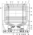
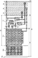
- FIG. 3 is a schematic plan view of a liquid crystal panel included in the liquid crystal display of Embodiment 1.
- FIG. FIG. 2 is a schematic cross-sectional view taken along the line AB in FIG. 1.
- 3 is a schematic plan view of a liquid crystal panel included in the liquid crystal display of Embodiment 1.
- FIG. 1 is a block diagram illustrating a configuration of a liquid crystal display according to Embodiment 1.
- FIG. 2 is a block diagram illustrating a configuration of a shift register in Embodiment 1.
- FIG. 3 is a circuit diagram of a unit circuit included in the shift register in Embodiment 1.
- FIG. 3 shows a timing chart of the shift register in Embodiment 1.
- 3 shows a timing chart of the shift register in Embodiment 1.
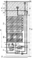
- FIG. 3 is a schematic plan view showing a configuration in a frame region of the liquid crystal display of Embodiment 1.
- FIG. 3 is a schematic plan view showing a configuration in a frame region of the liquid crystal display of Embodiment 1.
- FIG. 10 is a schematic cross-sectional view taken along line CD in FIG. 9.
- FIG. 10 is a schematic sectional view taken along line EF in FIG. 9.
- 6 is a diagram for explaining a manufacturing process for the liquid crystal display of Embodiment 1.
- FIG. 3 is a schematic plan view showing a configuration in a frame region of the liquid crystal display of Embodiment 1.
- FIG. 6 is a schematic plan view showing a configuration in a frame region of the liquid crystal display of Embodiment 2.
- FIG. 6 is a schematic plan view illustrating a configuration in a frame region of the liquid crystal display of Embodiment 3.
- FIG. 6 is a schematic plan view illustrating a configuration in a frame region of a liquid crystal display according to Embodiment 4.
- FIG. 10 is a schematic plan view illustrating a configuration in a frame region of a liquid crystal display according to a fifth embodiment. It is a plane schematic diagram which shows the structure in the frame area
- Embodiment 1 A liquid crystal display according to Embodiment 1 will be described with reference to FIGS. First, the overall structure of the liquid crystal display of the present embodiment will be described with reference to FIGS.
- the liquid crystal display of the present embodiment is an active matrix drive type and transmissive liquid crystal display, and includes a liquid crystal panel 1, a backlight (not shown) disposed behind the liquid crystal panel 1, the liquid crystal panel 1, and A control unit (not shown) for driving and controlling the backlight and a flexible substrate (not shown) for connecting the liquid crystal panel 1 to the control unit are provided.
- the liquid crystal panel 1 includes a display unit 2 that displays an image.
- a plurality of pixels 3 are arranged in a matrix.
- Each pixel 3 may be composed of sub-pixels of a plurality of colors (for example, three colors of red, green, and blue).
- the liquid crystal display of this embodiment may be a monochrome liquid crystal display. In this case, it is not necessary to divide each pixel 3 into a plurality of subpixels.
- the liquid crystal panel 1 is provided between an array substrate (active matrix substrate) 10 corresponding to the first substrate, a counter substrate 50 corresponding to the second substrate and facing the array substrate 10, and the substrates 10 and 50.
- An alignment film (not shown) provided and a source driver 5 mounted on the array substrate 10 are provided.
- the liquid crystal panel 1, the array substrate 10, and the counter substrate 50 include a region (display region) 7 corresponding to the display unit 2 and a region (frame region) 8 around the display region 7.
- the source driver 5 is a source bus line driving circuit described later.
- the seal 62 is formed in the frame area 8 so as to surround the display area 7.
- the seal 62 adheres the substrates 10 and 50 to each other and seals the liquid crystal layer 61 between the substrates 10 and 50.
- the array substrate 10 is provided on the back side of the liquid crystal display, and the counter substrate 50 is provided on the viewer side.
- the array substrate 10 is irradiated with light from the backlight, and an image displayed on the liquid crystal panel 1 is observed from the counter substrate 50 side.
- a polarizing plate (not shown) is attached on the surface of each substrate 10, 50 opposite to the liquid crystal layer 61. These polarizing plates are usually arranged in crossed Nicols.
- the source driver 5 is mounted by a COG (Chip On Glass) technique in a region of the array substrate 10 that does not face the counter substrate 50, that is, a region that protrudes from the counter substrate 50 (hereinafter also referred to as an overhang region).
- COG Chip On Glass
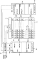
- the array substrate 10 vertically crosses the display area 7 with gate drivers 6a and 6b monolithically formed on the left and right sides of the display area 7, terminals 26, 27, 28, 29, and 30 formed in the overhang area.
- the source bus line (data signal line) 12 provided, the gate bus line (scanning signal line) 13 and the common bus line 17 provided so as to cross the display area 7, and the frame area 8 are formed respectively.
- the gate bus line 13 includes a gate bus line 13 connected to the output terminal of the left gate driver 6a and a gate bus line 13 connected to the output terminal of the right gate driver 6b, which are alternately arranged. ing.
- the gate bus line 13 corresponds to the bus line in the embodiment (D).
- a flexible substrate is mounted in a region where the terminals 26, 28, and 30 are provided (region surrounded by a thick two-dot chain line in FIG. 3).
- Each source bus line 12 is connected to the output section of the source driver 5 via a corresponding lead line 18 and terminal 27.
- Various signals and a power supply voltage are input from the control unit to the input unit of the source driver 5 through the flexible substrate, the terminal 28, the input wiring 25, and the terminal 29.
- a common signal is input to the common trunk line 16 from the control unit via the flexible substrate and the terminal 30.
- the common signal is a signal applied in common to all pixels.
- the common bus line 17 is connected to the common trunk line 16 in the frame region 8, and a common signal is applied to the common bus line 17 from the common trunk line 16.
- Gate drivers 6 a and 6 b Various signals and a power supply voltage are supplied to the gate drivers 6 a and 6 b from the control unit via the flexible substrate, the terminal 26 and the lead wire 19. Details will be described later.
- Gate drivers called gate monolithic, gate driverless, panel built-in gate driver, gate-in panel, gate-on-array, etc. can all be included in the gate drivers 6a and 6b. Instead of providing the two gate drivers 6a and 6b, only one gate driver that exhibits the same function as the two gate drivers 6a and 6b may be provided.
- the counter substrate 50 includes a transparent (translucent) insulating substrate 51, a black matrix (BM) 52 functioning as a light shielding member, and a plurality of columnar spacers (not shown).
- the BM 52 is formed so as to shield the frame area 8 and the area facing the bus line.
- the BM 52 is formed in a frame shape and covers the gate drivers 6a and 6b. In FIG. 2, the BM 52 is not shown in the display area 7.
- a plurality of color filters may be provided in the display area 7, and each color filter is formed so as to cover an area partitioned by the BM 52, that is, an opening of the BM 52.
- the counter substrate 50 may have a transparent (light transmissive) overcoat film that covers all the color filters.
- the columnar spacer is disposed in the light shielding region on the BM 52.
- a granular spacer (not shown) may be mixed in the seal 62.
- These spacers are members for making the distance between the array substrate 10 and the counter substrate 50 constant, and the distance (cell gap) between the two substrates is set to about 4.0 ⁇ m.
- the material for the color filter examples include an acrylic resin mixed with a pigment
- examples of the material for the BM52 include chrome and an acrylic resin mixed with a black pigment.
- the BM 52 has a thickness of about 1.0 ⁇ m and is formed from an acrylic resin mixed with a black pigment.
- the overcoat film is formed from a transparent insulating material. Specifically, a curable resin having optical transparency such as an acrylic resin or an epoxy resin is used.
- the overcoat film is preferably formed from an acrylic resin, and the thickness thereof is preferably about 2.0 ⁇ m.
- the overcoat film has a function of protecting the color filter physically or chemically.
- the liquid crystal mode of the liquid crystal display of this embodiment is not specifically limited.
- the counter substrate 50 In a liquid crystal mode using a vertical electric field such as a TN (Twisted Nematic) mode and a VA (Vertical Alignment) mode, the counter substrate 50 has a counter electrode to which a common signal is applied, and the array substrate 10 is common.
- a common transfer electrode 14 is connected to the main wiring 16, and both electrodes are connected to each other through a conductive member.
- the counter electrode is formed from a transparent conductive material (light-transmitting conductive material) such as indium tin oxide (ITO: Indium Tin Oxide), tin oxide (SnO 2 ), indium zinc oxide (IZO: Indium Zinc Oxide).
- ITO is preferably used.
- Examples of the conductive member include a curable resin mixed with conductive fine particles, silver, and carbon paste. Conductive fine particles may be mixed in the sealing material, and the fine particles may be used as a conductive member. Examples of the conductive fine particles include those obtained by coating resin fine particles with a metal such as gold.
- the liquid crystal display of this embodiment includes a pixel array 71, a display control circuit 72 provided in the control unit, a source driver 5, and gate drivers 6a and 6b.
- the pixel array 71 is formed on the n gate bus lines G1 to Gn corresponding to the gate bus line 13, the m source bus lines S1 to Sm corresponding to the source bus line 12, and the pixel 3, respectively.
- n and m are integers of 2 or more, i is an integer of 1 to n, and j is an integer of 1 to m.
- the gate bus lines G1 to Gn are arranged in parallel to each other, and the source bus lines S1 to Sm are arranged in parallel to each other so as to be orthogonal to the gate bus lines G1 to Gn.
- a pixel circuit Pij is arranged near the intersection of the gate bus line Gi and the source bus line Sj.
- the (m ⁇ n) pixel circuits Pij are arranged two-dimensionally, m in the row direction and n in the column direction.
- the gate bus line Gi is connected in common to the pixel circuit Pij arranged in the i-th row
- the source bus line Sj is connected in common to the pixel circuit Pij arranged in the j-th column.
- Each pixel circuit Pij is provided with a pixel TFT 4 as a switching element and a pixel electrode 9.
- the gate of the TFT 4 is connected to the gate bus line Gi, and one of the drain and the source of the TFT 4 is The other is connected to the pixel electrode 9 while being connected to the source bus line Sj.
- control signals such as a horizontal synchronization signal HSYNC and a vertical synchronization signal VSYNC, and an image signal DAT are supplied.
- the display control circuit 72 Based on these signals, the display control circuit 72 outputs the clock signals CK1, CK2, and the start pulse SP1 to the gate driver 6a, and the clock signals CK3, CK4, and the start pulse SP2 to the gate driver 6b.
- the control signal SC and the digital video signal DV are output to the source driver 5.
- the gate driver 6a includes a shift register 73a, and the shift register 73a includes a plurality of unit circuits SR1, SR3,.
- the unit circuits SR1, SR3,..., SRn-1 are connected to odd-numbered gate bus lines G1, G3,.
- the gate driver 6b includes a shift register 73b, and the shift register 73b includes a plurality of unit circuits SR2, SR4,.
- the unit circuits SR2, SR4,..., SRn are connected to the even-numbered gate bus lines G2, G4,.
- the shift registers 73a and 73b control the output signals SROUT1 to SROUTn to a high level (indicating a selected state) one by one in order.
- Output signals SROUT1 to SROUTn are applied to gate bus lines G1 to Gn, respectively. Accordingly, the gate bus lines G1 to Gn are sequentially selected one by one, and the pixel circuits Pij for one row are selected at a time. That is, the pixel TFT 4 of the pixel circuit Pij for one row is turned on.
- the source driver 5 applies a voltage corresponding to the digital video signal DV to the source bus lines S1 to Sm based on the control signal SC and the digital video signal DV. As a result, a voltage corresponding to the digital video signal DV is written into the pixel circuits Pij for one selected row. In this way, the liquid crystal display of the present embodiment displays an image.
- each of the unit circuits SR1 to SRn has input terminals INa and INb, clock terminals CKA and CKB, a power supply terminal VSS, and an output terminal OUT.
- the shift register 73a is supplied with a start pulse SP1, an end pulse EP1, two-phase clock signals CK1 and CK2, and a low-level potential VSS (for the sake of convenience, the same reference numerals as those of the power supply terminals). .
- the start pulse SP1 is input to the input terminal INa of the first stage unit circuit SR1 in the shift register 73a.
- the end pulse EP1 is input to the input terminal INb of the unit circuit SRn-1 at the final stage in the shift register 73a.
- the clock signal CK1 is input to the clock terminal CKA of the odd-numbered unit circuit in the shift register 73a and to the clock terminal CKB of the even-numbered unit circuit in the shift register 73a.
- the clock signal CK2 is input to the clock terminal CKA of the even-numbered unit circuit in the shift register 73a and to the clock terminal CKB of the odd-numbered unit circuit in the shift register 73a.
- the low level potential VSS is input to the power supply terminal VSS of all the unit circuits in the shift register 73a.
- the output signals SROUT1, SROUT3,..., SROUTn-1 are output from the output terminals OUT of the unit circuits SR1, SR3,..., SRn-1, respectively, and the output signals SROUT1, SROUT3,.
- ⁇ 1 is output to the gate bus lines G1, G3,..., Gn ⁇ 1, respectively.
- Each output signal includes an input terminal INa of the unit circuit after two stages (one stage after when considered in the shift register 73a) and an input terminal of the unit circuit four stages before (when considered within the shift register 73a). It is input to INb.
- a start pulse SP2, an end pulse EP2, two-phase clock signals CK3 and CK4, and a low level potential VSS are supplied to the shift register 73b.
- the start pulse SP2 is input to the input terminal INa of the first stage unit circuit SR2 in the shift register 73b.
- the end pulse EP2 is input to the input terminal INb of the unit circuit SRn at the final stage in the shift register 73b.
- the clock signal CK3 is input to the clock terminal CKA of the odd-numbered unit circuit in the shift register 73b and to the clock terminal CKB of the even-numbered unit circuit in the shift register 73b.
- the clock signal CK4 is input to the clock terminal CKA of the even-numbered unit circuit in the shift register 73b and to the clock terminal CKB of the odd-numbered unit circuit in the shift register 73b.
- the low level potential VSS is input to the power supply terminal VSS of all the unit circuits in the shift register 73b.
- the output signals SROUT2, SROUT4,..., SROUTn are output from the output terminals OUT of the unit circuits SR2, SR4,..., SRn, respectively, and the output signals SROUT2, SROUT4,. Output to the gate bus lines G2, G4,..., Gn.
- Each output signal includes an input terminal INa of the unit circuit after two stages (one stage after when considered in the shift register 73b) and an input terminal of the unit circuit four stages before (when considered within the shift register 73b). It is input to INb.
- the low level potential VSS is preferably a negative potential from the viewpoint of surely turning off the n-channel TFT.
- the low-level potential VSS is positive.
- the potential may be
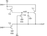
- each unit circuit includes transistors Tr1 to Tr4, which are n-channel TFTs, and a capacitor (hereinafter also referred to as a bootstrap capacitor) CB1.
- the transistor Tr1 is also referred to as an output transistor Tr1.
- the output transistor Tr1 has a drain connected to the clock terminal CKA and a source connected to the output terminal OUT.
- the transistor Tr2 has a drain and a gate connected to the input terminal INa, and a source connected to the gate of the output transistor Tr1.
- the bootstrap capacitor CB1 is provided between the gate and the source of the output transistor Tr1, and one terminal is connected to the gate of the output transistor Tr1, and the other terminal is connected to the output terminal OUT.
- the transistor Tr3 has a drain connected to the output terminal OUT, a gate connected to the clock terminal CKB, and a source connected to the power supply terminal VSS.
- the transistor Tr4 has a drain connected to the gate of the output transistor Tr1, a gate connected to the input terminal INb, and a source connected to the power supply terminal VSS.
- the output transistor Tr1 is provided between the clock terminal CKA and the output terminal OUT, and functions as a transistor (transmission gate) that switches whether or not to pass the clock signal according to the gate potential.
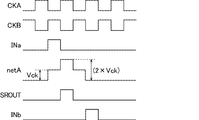
- the gate of the output transistor Tr1 is capacitively coupled to a conduction terminal (source) on the output terminal OUT side. Therefore, as will be described later, in a period in which the output transistor Tr1 is on and the clock signal CK1 or CK3 (hereinafter also referred to as clock signal CKA) input to the clock terminal CKA is at a high level, The gate potential becomes higher than the high level potential of the clock signal CKA.
- netA the node to which the gate of the output transistor Tr1 is connected
- FIG. 7 and 8 show timing charts of the shift registers 73a and 73b.
- FIG. 7 shows the input / output signals of the odd-numbered unit circuits and the voltage change of the node netA in each shift register.
- the clock signal CK1 or CK3 is input to the odd-numbered unit circuit in each shift register through the clock terminal CKA, and the clock signal CK2 or CK4 is input through the clock terminal CKB.
- the A period in which the potentials of the clock signals CK1 to CK4 are at a high level is substantially the same as a half cycle.
- the clock signal CK2 delays the clock signal CK1 by 1 ⁇ 2 period
- the clock signal CK3 delays the clock signal CK1 by 1 ⁇ 4 period
- the clock signal CK4 delays the clock signal CK2 by 1 ⁇ 4 period, respectively.
- the start pulses SP1 and SP2 become high level for the same length of time as the period of the clock signals CK2 and CK4 being high level before the start of the shift operation, respectively.
- the end pulses EP1 and EP2 (not shown in FIGS. 7 and 8) become high level for the same length of time as the potential of the clock signals CK2 and CK4, respectively, after the end of the shift operation.
- a signal start pulse SP1, SP2 or an output signal of a unit circuit in the previous stage (one stage before when considered in each shift register) input to the input terminal INa.
- start pulse SP1, SP2 or an output signal of a unit circuit in the previous stage input to the input terminal INa.
- INa also referred to as an input signal INa.
- a signal input to the input terminal INb (end pulse EP1, EP2, or the output signal of the unit circuit after four stages (after two stages in each shift register), hereinafter also referred to as the input signal INb).
- the transistor Tr4 Changes from low level to high level, the transistor Tr4 is turned on.
- the transistor Tr4 is turned on, the low level potential VSS is applied to the node netA, the potential of the node netA changes to the low level, and the output transistor Tr1 is turned off.
- the transistor Tr4 is turned off. At this time, the node netA is in a floating state, but the output transistor Tr1 is kept off. Ideally, the output transistor Tr1 is kept off and the output signal SROUT is kept low until the input signal INa becomes the next high level.
- the transistor Tr3 is turned on when the clock signal CKB is at a high level. Therefore, every time the clock signal CKB becomes high level, the low level potential VSS is applied to the output terminal OUT. As described above, the transistor Tr3 has a function of repeatedly setting the output terminal OUT to the low level potential VSS and stabilizing the output signal SROUT.
- Even-numbered unit circuits operate in the same manner as odd-numbered unit circuits.
- gate pulses are sequentially output to the gate bus lines G1, G2, G3,.
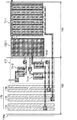
- each gate driver is provided with a wiring group 78 extending in a direction perpendicular to the gate bus line 13 described above.
- the wiring group 78 includes a wiring 74 set to the low level potential VSS, a wiring 75 that transmits the clock signal CK1 or CK3, and a wiring 76 that transmits the clock signal CK2 or CK4.
- a slit-shaped opening is formed in each wiring.
- the output transistor Tr1 and the bootstrap capacitor CB1 are disposed adjacent to each other.
- the transistors Tr2 to Tr4 are arranged adjacent to each other.
- a region (hereinafter also referred to as a control element region) 77 in which the transistors Tr2 to Tr4 are disposed is located between the wiring group 78 and the output transistor Tr1.
- the output transistor Tr1 and the bootstrap capacitor CB1 are disposed on the control element region 77 and the end portion 10a side of the wiring group 78 (opposite the display region 7).
- the array substrate 10 includes a band-like region (hereinafter also referred to as a seal application region) 63 sandwiched between thick broken lines, and the seal 62 does not protrude from the seal application region 63. Thus, it is formed in a strip shape on the seal application region 63.
- One end of the seal application region 63 is set in a region between the bootstrap capacitor CB1 and the end 10a of the array substrate 10, and the other end is in a region between the wiring 74 and the display region 7.
- the seal application region 63 includes a region 65 where the transistors Tr2 to Tr4 and the wirings 74 to 76 (wiring group 78) are disposed, and a region 64 where the output transistor Tr1 and the bootstrap capacitor CB1 are disposed. It is out.
- the region 65 corresponds to the first region
- the region 64 corresponds to the second region.
- the output transistor Tr1 and the bootstrap capacitor CB1 are arranged in the seal application region 63.
- the seal 62 is disposed so as to cover at least part or all of the output transistor Tr1 and part or all of the control element region 77. As long as it does not protrude from the seal application region 63, it is not particularly limited whether or not the region other than these covers the seal 62.
- the seal 62 may be disposed so as to cover a part or all of the output transistor Tr1, the entire region of the control element region 77, and a part or all of the wiring 76, or the bootstrap capacitor CB1. It may be arranged so as to cover part or all, all of the output transistor Tr1, all regions of the control element region 77, all of the wiring 76, and part or all of the wiring 75, or bootstrap.
- the seal 62 includes the first portion adjacent to the liquid crystal layer 61 and the second portion adjacent to the first portion. The first portion is disposed on the region 65, and the second portion is the region. 64.
- Each of the transistors Tr1 to Tr4 is a bottom gate type thin film transistor.
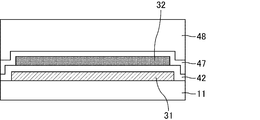
- the output transistor Tr1 is large in size and has a comb-like source / drain structure. Thereby, a large channel width of, for example, about several tens of ⁇ m to several hundreds of mm is secured.
- the array substrate 10 includes a transparent (translucent) insulating substrate 11, and the output transistor Tr ⁇ b> 1 includes a gate electrode 41 on the insulating substrate 11 and a gate on the gate electrode 41. It has an insulating film 42, an i layer (semiconductor active layer) 43 on the gate insulating film 42, an n + layer 44 on the i layer 43, and a source electrode 45 and a drain electrode 46 respectively provided on the n + layer 44. is doing.
- Each of the source electrode 45 and the drain electrode 46 has a plurality of comb teeth, and the source electrode 45 and the drain electrode 46 are arranged to face each other so that the comb teeth are engaged with each other.
- the bootstrap capacitor CB1 includes a first electrode 31 on the insulating substrate 11, a gate insulating film 42 provided on the first electrode 31, and shared with the output transistor Tr1, and gate insulation. And a second electrode 32 on the film 42.
- the insulating substrates 11 and 51 are mainly made of an inorganic material such as glass, quartz glass, or silicon nitride, or an organic polymer compound such as an acrylic resin ( Resin) or the like.
- an inorganic material such as glass, quartz glass, or silicon nitride
- an organic polymer compound such as an acrylic resin ( Resin) or the like.
- quartz glass having a thickness of about 0.7 mm.
- the gate electrode 41 and the first electrode 31 are formed of the same conductive film containing materials such as molybdenum (Mo), titanium (Ti), aluminum (Al), copper (Cu), and alloys thereof.
- the gate electrode 41 and the first electrode 31 may be formed from a laminated film of these conductive films.
- Al is used.
- the gate insulating film 42 is formed of a transparent (translucent) insulating film containing an inorganic insulating material such as silicon nitride or silicon oxide.
- the gate insulating film 42 may be formed using a laminated film of these insulating films.
- the i layer (semiconductor active layer) 43 is made of amorphous silicon, and the n + layer 44 is made of amorphous silicon containing an impurity (for example, phosphorus).
- the source electrode 45, the drain electrode 46, and the second electrode 32 are formed from the same conductive film containing materials such as Mo, Ti, Al, Cu, and alloys thereof.
- the source electrode 45, the drain electrode 46, and the second electrode 32 may be formed of a laminated film of these conductive films.
- a transparent (translucent) insulating film 47 that functions as a passivation film is formed on the source electrode 45, the drain electrode 46, and the second electrode 32.
- the insulating film 47 is formed from an inorganic insulating film such as a silicon nitride film or a silicon oxide film.
- the insulating film 47 may be formed using a laminated film of these inorganic insulating films.
- a transparent (translucent) insulating film 48 that functions as a planarizing film is formed on the insulating film 47.
- the insulating film 48 is formed from an organic insulating film. Examples of the material for the organic insulating film include a photosensitive resin such as a photosensitive acrylic resin.
- the transistors Tr2 to Tr4 are different from the output transistor Tr1 only in the planar structure, and the cross-sectional structure is the same as that of the output transistor Tr1.
- the hatched member, the gate electrode 41, and the first electrode 31 are formed of the same conductive film
- the electrode 46 and the second electrode 32 are formed of the same conductive film.
- a white square region arranged in a region where a hatched member and a dot-shaped member overlap each other is a contact hole for connecting both members to each other Is shown.
- the pixel TFT 4 is a bottom-gate thin film transistor, like the output transistors Tr1 to Tr4, and is formed together with the output transistors Tr1 to Tr4 through the same process.
- the above-described pixel electrode 9 is formed on the insulating film 48 in the display region 7.
- the pixel electrode 9 is electrically connected to the drain electrode (not shown) of the pixel TFT 4 through a contact hole (not shown) that penetrates the insulating films 47 and 48.
- the pixel electrode 9 is made of a transparent conductive material (a conductive material having optical transparency) such as ITO, SnO 2 , or IZO.
- the liquid crystal display of the present embodiment can be manufactured by a general method, but more specifically, first, a substrate before being divided into a plurality of array substrates 10 (hereinafter also referred to as array mother glass). And the board
- substrate 50 is each produced by a normal method.
- steps S11 to S19 are performed as shown in FIG.
- step S11 substrate cleaning process
- the array mother glass and the CF mother glass are cleaned.
- step S11 and step S12 you may implement a degassing process between step S11 and step S12.
- the array mother glass and the CF mother glass are heated to remove unnecessary substances such as organic solvents and gases from these mother glasses.
- step S12 alignment film forming step
- alignment films are formed on the array mother glass and the CF mother glass, respectively.
- the material for the alignment film include organic materials such as polyimide and inorganic materials such as silicon oxide.
- step S13 rubbing process
- each alignment film is rubbed.
- step S13 may be omitted depending on the alignment state of the liquid crystal molecules in the liquid crystal layer 61. Moreover, it may replace with a rubbing process and may perform orientation processes other than a rubbing process, for example, a photo-alignment process.
- a seal material before curing (hereinafter also referred to as a seal material) to either the array mother glass or the CF mother glass by a method such as a screen printing method or a dispenser drawing method. .) Is applied.
- the sealing material is pasty and is applied in a closed ring shape.
- This sealing material is a material having curable properties (for example, ultraviolet curable property) and thermosetting property (hereinafter also referred to as a combined light / heat type sealing material).
- curable properties for example, ultraviolet curable property
- thermosetting property hereinafter also referred to as a combined light / heat type sealing material.
- an acrylic resin and / or an epoxy resin is used. Including.
- the light / heat combination type sealing material include, for example, Photorec S series (manufactured by Sekisui Chemical Co., Ltd.) mainly composed of an epoxy acrylic resin.
- the sealing material is preferably applied by a dispenser drawing method.
- step S15 liquid crystal material dropping and bonding step
- a liquid crystal material is dropped on the mother glass coated with the sealing material, the mother glass not coated, or both mother glasses, and both mothers Glue the glass together.
- the two mother glasses are bonded together under an environment lower than atmospheric pressure (for example, under vacuum). After bonding, both mother glasses are placed under atmospheric pressure.
- the liquid crystal material is preferably dropped on the mother glass for CF.
- step S16 the sealing material is irradiated with light from the array mother glass side to cure (preliminarily cure) the sealing material to some extent.
- the light is blocked by the output transistor Tr1 and the bootstrap capacitor CB1
- the light irradiated on the seal material is insufficient on the output transistor Tr1 and the bootstrap capacitor CB1, and the seal material is hardly temporarily cured.
- the region 65 in which the transistors Tr2 to Tr4 and the wirings 74 to 76 are disposed includes many light transmitting regions, the sealing material can be sufficiently preliminarily cured on the region 65.
- the temporarily cured sealing material portion (the portion corresponding to the first portion) is disposed closer to the display area 7, and the sealing material portion that has not been temporarily cured (the portion corresponding to the second portion) is an array.
- the substrate 10 is disposed closer to the end 10a. Therefore, it is possible to prevent the sealing material portion that has not been temporarily cured from coming into contact with the liquid crystal layer, and as a result, it is possible to prevent the sealing material component from being dissolved and diffused in the liquid crystal layer.
- light is irradiated from the array substrate 10 side because the BM 52 is formed on the counter substrate 50.
- the kind of light to irradiate is not specifically limited, For example, the light containing an ultraviolet-ray is mentioned. Preferably, ultraviolet rays are used.
- step S17 the bonded mother glass is heated.
- the sealing material is further cured (mainly cured).
- the entire sealing material is cured. Therefore, the seal material is hardly temporarily cured in step S16 on the region 64 where the output transistor Tr1 and the bootstrap capacitor CB1 are disposed, and is fully cured in step S17.
- the sealing material is temporarily cured in step S16 and finally cured in step S17 on the region 65 where the transistors Tr2 to Tr4 and the wirings 74 to 76 are disposed.
- the sealing material portion (the portion corresponding to the first portion) that is temporarily cured and permanently cured is disposed closer to the display region 7, and the sealing material portion (not described above) that is permanently cured without being temporarily cured.
- the portion corresponding to the second portion is disposed closer to the end portion 10a of the array substrate 10.
- steps S16 and S17 can be set as appropriate according to the characteristics of the sealing material.
- the Photorec S series for example, ultraviolet rays of about 10 J are irradiated at 120 ° C. Heat treatment is performed for 60 minutes.
- step S18 the bonded mother glass is divided by a panel dividing line and divided into a plurality of liquid crystal cells.
- step S19 the liquid crystal cell is inspected such as a lighting inspection to confirm the quality state of the liquid crystal cell.
- a polarizing plate and a phase plate are pasted on both surfaces of the liquid crystal cell, and then the source driver 5 is mounted to complete the liquid crystal panel 1.
- a flexible substrate is connected to the liquid crystal panel 1, a control part and a backlight unit are attached, and these are accommodated in a housing
- the output transistor Tr1 and the bootstrap capacitor CB1 are arranged in a region between the end 10a of the array substrate 10 and the control element region 77. Therefore, each transistor in the control element region 77 and the wiring group 78 can be arranged on the display region 7 side of the output transistor Tr1 and the bootstrap capacitor CB1. Further, the sealing material can be temporarily cured and fully cured on the region 65 where the transistors Tr2 to Tr4 and the wirings 74 to 76 are disposed, while the region where the output transistor Tr1 and the bootstrap capacitor CB1 are disposed. The sealant can be fully cured on 64. As a result, the sealing material component can be prevented from dissolving in the liquid crystal layer before the seal main curing process is completed. Further, the seal application region 63 can be set widely. Furthermore, the occurrence of liquid crystal leakage can be suppressed. Therefore, it is possible to reduce the occurrence of defects in quality and improve the adhesive strength between the substrates.
- each element and the thickness of each wiring are not particularly limited and can be set as appropriate.
- the thickness of the wirings 74 and 75 is substantially the same as that of the wiring 76.
- the interval between the wiring 74 and the wiring 75 can be set to 30 ⁇ m.
- the pitch of the output transistors is substantially equal to the pitch of the unit circuits or the gate bus lines.
- the width of the wiring connecting the elements or between the elements and the wiring can be set to 10 ⁇ m, for example.
- the ratio of the area shielded from light in the region A is preferably 50% or less, and the ratio of the area shielded from light in the region B is preferably larger than 50%.
- the liquid crystal display of the second embodiment is substantially the same as the liquid crystal display of the first embodiment except that the layout of elements and wirings in the shift register is different but different.
- the wiring group 78 is arranged in a region between the transistors Tr2 to Tr4 (control element region 77) and the display region 7.
- the transistors Tr2 to Tr4 are arranged in a region between the wiring group 78 and the display region 7.
- the first and second embodiments have a common feature in that the wiring group 78 and the transistors Tr2 to Tr4 (control element region 77) are arranged in a region between the display region 7 and the output transistor Tr1.
- the array substrate 10 includes a band-like region (hereinafter also referred to as a seal application region) 63 sandwiched between thick broken lines, and the seal 62 does not protrude from the seal application region 63. It is formed in a band shape.
- One end of the seal application region 63 is set in a region between the bootstrap capacitor CB1 and the end 10a of the array substrate 10, and the other end includes transistors Tr2 to Tr4 (control element region 77). It is set in an area between the display area 7.
- the seal application region 63 includes a region 64 in which the output transistor Tr1 and the bootstrap capacitor CB1 are disposed, transistors Tr2 to Tr4 (control element region 77), and wirings 74 to 76 (wiring group 78).
- a region 66 corresponds to the first region, and the region 64 corresponds to the second region.
- the output transistor Tr1 and the bootstrap capacitor CB1 are arranged in the seal application region 63.
- the seal 62 is disposed so as to cover at least part or all of the output transistor Tr1 and part or all of the wiring group 78. As long as it does not protrude from the seal application region 63, it is not particularly limited whether or not the region other than these covers the seal 62.
- the seal 62 may be disposed so as to cover the entire output transistor Tr1, the entire wiring group 78, a partial region or the entire region of the control element region 77, or one of the bootstrap capacitors CB1.
- all or part of the output transistor Tr 1, the entire wiring group 78, and a part or all of the control element region 77 may be disposed.
- the seal 62 includes the first portion adjacent to the liquid crystal layer 61 and the second portion adjacent to the first portion. The first portion is disposed on the region 66, and the second portion is the region. 64.
- the output transistor Tr1 and the bootstrap capacitor CB1 are arranged in a region between the end portion 10a of the array substrate 10 and the control element region 77. Therefore, also in this embodiment, it is possible to reduce the occurrence of defects in quality and improve the adhesive strength between the substrates.
- the arrangement locations of the output transistor Tr1 and the bootstrap capacitor CB1 may be interchanged.
- the liquid crystal display according to the third embodiment is substantially the same as the liquid crystal display according to the first embodiment except that the layout of elements and wirings in the shift register is different.
- the transistors Tr2 to Tr4 (control element region 77) are arranged in a region between the end 10a of the array substrate 10 and the bootstrap capacitor CB1.
- the array substrate 10 includes a band-like region (hereinafter also referred to as a seal application region) 63 sandwiched between thick broken lines, and the seal 62 does not protrude from the seal application region 63. It is formed in a band shape.
- One end of the seal application region 63 is set in a region between the control element region 77 and the end 10 a of the array substrate 10, and the other end is in a region between the wiring 74 and the display region 7. Is set.
- the seal application region 63 includes a region 64 where the output transistor Tr1 and the bootstrap capacitor CB1 are disposed, a region 67 where the transistors Tr2 to Tr4 are disposed, and wirings 74 to 76 (wiring group 78). And a region 68 that is formed.
- the region 68 corresponds to the first region
- the region 64 corresponds to the second region.
- the output transistor Tr1 and the bootstrap capacitor CB1 are arranged in the seal application region 63.
- the seal 62 is disposed so as to cover at least part or all of the output transistor Tr ⁇ b> 1 and part or all of the wiring 76. As long as it does not protrude from the seal application region 63, it is not particularly limited whether or not the region other than these covers the seal 62.
- the seal 62 may be disposed so as to cover part or all of the bootstrap capacitor CB1, all of the output transistor Tr1, and all of the wiring 76, or part of the control element region 77.
- it may be arranged so as to cover the entire region, the entire bootstrap capacitor CB1, the entire output transistor Tr1, the entire wiring 76, and a part or all of the wiring 75, or the control element region 77.
- the seal 62 includes the first portion adjacent to the liquid crystal layer 61 and the second portion adjacent to the first portion. The first portion is disposed on the region 68, and the second portion is the region. 64.
- the output transistor Tr1 and the bootstrap capacitor CB1 are disposed in a region between the end 10a of the array substrate 10 and the wiring 76. Therefore, the wiring group 78 can be disposed on the display region 7 side of the output transistor Tr1 and the bootstrap capacitor CB1. Further, the sealing material can be temporarily cured and main-cured on the region 68 where the wirings 74 to 76 are disposed, while the sealing material is disposed on the region 64 where the output transistor Tr1 and the bootstrap capacitor CB1 are disposed. Can be fully cured. As a result, the sealing material component can be prevented from dissolving in the liquid crystal layer before the seal main curing process is completed. Further, the seal application region 63 can be set widely. Furthermore, the occurrence of liquid crystal leakage can be suppressed. Therefore, as in the first embodiment, it is possible to reduce the occurrence of defects in quality and improve the adhesive strength between the substrates.
- the present embodiment is different from the first embodiment in that the seal material portion to be temporarily cured and to be fully cured is arranged separately.
- the liquid crystal display according to the fourth embodiment is substantially the same as the liquid crystal display according to the third embodiment except that the layout of elements and wirings in the shift register is different.
- the transistors Tr2 to Tr4 are arranged in a region between the end 10a of the array substrate 10 and the bootstrap capacitor CB1.
- the wiring group 78 is disposed in a region between the end 10a of the array substrate 10 and the output transistor Tr1.
- the third and fourth embodiments have a common feature in that the output transistor Tr1 and the bootstrap capacitor CB1 are arranged in a region between the wiring group 78 and the transistors Tr2 to Tr4 (control element region 77). .
- the array substrate 10 includes a band-like region (hereinafter also referred to as a seal application region) 63 sandwiched between thick broken lines, and the seal 62 does not protrude from the seal application region 63. It is formed in a band shape.
- One end of the seal application region 63 is set between the wiring 74 and the end 10a, and the other end is set in a region between the transistors Tr2 to Tr4 (control element region 77) and the display region 7.
- the seal application region 63 includes a region 64 in which the output transistor Tr1 and the bootstrap capacitor CB1 are disposed, a region 67 in which the transistors Tr2 to Tr4 are disposed, and wirings 74 to 76 (wiring group 78).
- the region 67 corresponds to the first region
- the region 64 corresponds to the second region.
- the output transistor Tr1 and the bootstrap capacitor CB1 are arranged in the seal application region 63.
- the seal 62 is disposed so as to cover at least a part or the whole of the bootstrap capacitor CB1 and a part or the whole of the control element region 77. As long as it does not protrude from the seal application region 63, it is not particularly limited whether or not the region other than these covers the seal 62.
- the seal 62 may be disposed so as to cover a part or the whole of the output transistor Tr1, the whole of the bootstrap capacitor CB1, and a part or the whole of the control element region 77. It may be arranged so as to cover a part or all of 76, all of the output transistor Tr 1, all of the bootstrap capacitor CB 1, and part or all of the control element region 77.
- the seal 62 includes the first portion adjacent to the liquid crystal layer 61 and the second portion adjacent to the first portion. The first portion is disposed on the region 67, and the second portion is the region. 64.
- the output transistor Tr1 and the bootstrap capacitor CB1 are arranged in a region between the end portion 10a of the array substrate 10 and the control element region 77. Therefore, also in this embodiment, it is possible to reduce the occurrence of defects in quality and improve the adhesive strength between the substrates.
- the wiring group 78 is disposed in a region between the end portion 10a of the array substrate 10 and the output transistor Tr1. Therefore, the transistors Tr1 to Tr4 can be protected from the static electricity entering from the outside by the wiring group 78.
- the arrangement locations of the output transistor Tr1 and the bootstrap capacitor CB1 may be interchanged.
- the liquid crystal display of the fifth embodiment is substantially the same as the liquid crystal display of the first embodiment except that the layout of elements and wirings in the shift register is different.
- the transistors Tr2 to Tr4 (control element region 77) are arranged in a region between the display region 7 and the bootstrap capacitor CB1, and the wiring group 78 is Are arranged in a region between the output transistor Tr1 and the bootstrap capacitor CB1.
- the array substrate 10 includes a band-like region (hereinafter also referred to as a seal application region) 63 sandwiched between thick broken lines, and the seal 62 does not protrude from the seal application region 63. It is formed in a band shape.
- One end of the seal application region 63 is set in a region between the output transistor Tr1 and the end 10a of the array substrate 10, and the other end is connected to the transistors Tr2 to Tr4 (control element region 77) and the display region. 7 is set in the area between the two.
- the seal application region 63 includes a region 69 where the output transistor Tr1 is disposed, a region 70 where the bootstrap capacitor CB1 is disposed, a region 67 where the transistors Tr2 to Tr4 are disposed, and wirings 74 to 76 ( And a region 79 in which the wiring group 78) is arranged. Regions 67 and 79 correspond to the first region, and regions 69 and 70 correspond to the second region. Thus, in the present embodiment, unlike the comparative embodiment 1, the output transistor Tr1 and the bootstrap capacitor CB1 are arranged in the seal application region 63.
- the seal 62 is disposed so as to cover (1) at least part or all of the output transistor Tr1 and part or all of the wiring 74, or (2) part or all of the bootstrap capacitor CB1.
- the control element region 77 is disposed so as to cover at least a partial region or the entire region.
- the seal 62 includes a first part adjacent to the liquid crystal layer 61 and a second part adjacent to the first part. In each of the cases (1) and (2), whether or not the seal 62 covers the area other than the above unless it protrudes from the seal application area 63 and the first portion is not disposed on the bootstrap capacitor CB1. Is not particularly limited.
- the seal 62 may be disposed so as to cover the entire output transistor Tr1 and the entire wiring group 78, or a part or all of the output transistor Tr1 and the wiring group 78. It may be arranged so as to cover all, all of the bootstrap capacitor CB1, and a part or all of the control element region 77.
- the seal 62 may be disposed so as to cover the entire bootstrap capacitor CB1 and the entire region of the control element region 77, or a part or all of the wiring group 78
- the bootstrap capacitor CB1 may be disposed so as to cover all or part of the control element region 77, or part or all of the output transistor Tr1, all of the wiring group 78
- the bootstrap capacitor CB1 may be disposed so as to cover the entire part of the control element region 77 or the entire region.
- the output transistor Tr1 is disposed in a region between the end 10a of the array substrate 10 and the wiring group 78, and the bootstrap capacitor CB1 is connected to the end 10a of the array substrate 10 and the control element. It is arranged in a region between the regions 77. Therefore, the wiring group 78 can be disposed on the display region 7 side of the output transistor Tr1, and the control element region 77 can be disposed on the display region 7 side of the bootstrap capacitor CB1. Further, the sealing material can be temporarily cured and fully cured in the region 67 where the transistors Tr2 to Tr4 are disposed and the region 79 where the wiring group 78 is disposed.
- the seal material can be fully cured on the region 69 where the output transistor Tr1 is disposed and on the region 70 where the bootstrap capacitor CB1 is disposed.
- the sealing material component can be prevented from dissolving in the liquid crystal layer before the seal main curing process is completed.
- the seal application region 63 can be set widely. Furthermore, the occurrence of liquid crystal leakage can be suppressed. Therefore, as in the first embodiment, it is possible to reduce the occurrence of defects in quality and improve the adhesive strength between the substrates.
- the present embodiment is different from the first embodiment in that the seal material portion to be temporarily cured and to be fully cured is arranged separately.
- the placement locations of the output transistor Tr1 and the bootstrap capacitor CB1 may be interchanged, and the placement locations of the control element region 77 and the wiring group 78 may be interchanged.
- the semiconductor material of each TFT is not particularly limited and can be appropriately selected.
- a group 14 element semiconductor such as silicon, an oxide semiconductor, or the like can be given.
- the crystallinity of the semiconductor material of each TFT is not particularly limited, and may be single crystal, polycrystal, amorphous, or microcrystal, and may include two or more of these crystal structures.
- the output transistor includes amorphous silicon
- the channel width of the output transistor and the size of the bootstrap capacitor are particularly large from the viewpoint of increasing the driving capability. Therefore, when the output transistor includes amorphous silicon, it is possible to remarkably exhibit the effect of reducing the occurrence of defects in quality and improving the adhesive strength of the seal.
- the oxide semiconductor includes oxygen (O) and at least one element selected from the group consisting of indium (In), gallium (Ga), zinc (Zn), aluminum (Al), and silicon (Si). It is preferable that In, Ga, Zn, and O are included.
- each TFT is not particularly limited to the bottom gate type, and can be appropriately selected.
- TFTs other than gate driver TFTs may be further arranged in the frame region.
- the number of unit circuits satisfying the above-described layout and the arrangement location are not particularly limited, and can be set as appropriate. That is, it is sufficient that at least one unit circuit includes any one of the layouts described above, and some or all of the unit circuits may include any one of the layouts described above. However, it is preferable that all the unit circuits include any one of the above-described layouts from the viewpoint of exhibiting the above-described effects particularly effectively.
- each gate driver is not particularly limited except for the output transistor and the bootstrap capacitor, and can be determined as appropriate.
- the first to fifth embodiments may be combined with each other.
- unit circuits with different layouts may be formed in the same shift register, or a plurality of shift registers include unit circuits with different layouts. May be.
- Pixel 4 TFT for pixel 5: Source bus line drive circuit (source driver) 6a, 6b: gate bus line drive circuit (gate driver) 7: Display region 8: Frame region 9: Pixel electrode 10: Array substrate 10a: End 11: Insulating substrate 12, S1 to Sm: Source bus line 13, G1 to Gn: Gate bus line 14: Common transfer electrode 16: Common trunk line 17: Common bus line 18, 19: Lead line 25: Input lines 26, 27, 28, 29, 30: Terminal 31: First electrode 32: Second electrode 41: Gate electrode 42: Gate insulating film 43: i layer (semiconductor active layer) 44: n + layer 45: source electrode 46: drain electrode 47, 48: insulating film 50: counter substrate 51: insulating substrate 52: black matrix (BM) 61: liquid crystal layer 62: seal 63: seal application areas 64 to 69, 70, 79: area 71: pixel array 72: display control circuits 73a, 73b: shift registers 74 to 76: wiring
- BM black matrix
Landscapes
- Physics & Mathematics (AREA)
- Nonlinear Science (AREA)
- Crystallography & Structural Chemistry (AREA)
- Chemical & Material Sciences (AREA)
- General Physics & Mathematics (AREA)
- Engineering & Computer Science (AREA)
- Optics & Photonics (AREA)
- Mathematical Physics (AREA)
- Computer Hardware Design (AREA)
- Theoretical Computer Science (AREA)
- Microelectronics & Electronic Packaging (AREA)
- Power Engineering (AREA)
- Liquid Crystal (AREA)
- Liquid Crystal Display Device Control (AREA)
- Control Of Indicators Other Than Cathode Ray Tubes (AREA)
- Devices For Indicating Variable Information By Combining Individual Elements (AREA)
Abstract
Description
比較形態1に係る液晶ディスプレイは、アレイ基板と、対向基板と、両基板を互いに貼り合わせるためのシールと、アレイ基板上にモノリシック形成されたシフトレジスタとを備えている。シフトレジスタは、ゲートバスラインに接続された出力トランジスタTr11と、出力トランジスタTr11に接続されたブートストラップ・コンデンサCB11と、トランジスタTr12~Tr14と、配線174~176からなる配線群178とを有している。
前記第1基板は、絶縁基板と、前記絶縁基板上にモノリシック形成されたシフトレジスタと、複数のバスラインと、第1端部と、表示領域とを含み、
前記シフトレジスタは、多段接続された複数の単位回路と、前記複数の単位回路に接続された配線とを含み、かつ、前記第1端部及び前記表示領域の間の領域内に配置され、
前記複数の単位回路は少なくとも一つは、
クロック信号が入力されるクロック端子と、
対応するバスラインに接続され、出力信号が出力される出力端子と、
ソース及びドレインの一方が前記クロック端子に接続され、前記ソース及び前記ドレインの他方が前記出力端子に接続された第1トランジスタ(出力トランジスタ)と、
第2トランジスタと、
第1端子が前記第1トランジスタのゲートに接続され、第2端子が前記出力端子に接続されたコンデンサ(ブートストラップ・コンデンサ)とを含み、
前記第1トランジスタ及び前記コンデンサは、前記第1端部と、前記配線又は前記第2トランジスタとの間の領域内に配置される液晶ディスプレイ(以下、「本発明に係るディスプレイ」とも言う。)である。
なお、前記シフトレジスタは、前記配線を複数有してもよいし、前記少なくとも一つの単位回路は、前記第2トランジスタを複数有してもよい。これらの場合、前記複数の配線の用途は通常、互いに異なり、前記複数の第2トランジスタの用途は通常、互いに異なる。
前記シールは、前記液晶層に隣接する第1部分と、前記第1部分に隣接する第2部分とを含み、
前記第1部分は、前記第1領域上に配置され、
前記第2部分は、前記第2領域上に配置されることが好ましい。
前記配線及び前記第2トランジスタの他方は、前記第1トランジスタ及び前記コンデンサの間の領域内に配置されてもよい。
前記複数の画素回路は各々、画素用トランジスタと、前記画素用トランジスタに接続された画素電極とを含み、
前記複数のバスラインは各々、対応する複数の画素用トランジスタのゲートに接続されることが好ましい。
図1~14を参照して、実施形態1の液晶ディスプレイについて説明する。まず、図1~3を参照して、本実施形態の液晶ディスプレイの全体の構造について説明する。
まず、入力端子INaに入力される信号(スタートパルスSP1、SP2、又は、前々段(各シフトレジスタ内で考えると一段前)の単位回路の出力信号。以下、入力信号INaとも言う。)がローレベルからハイレベルに変化すると、ダイオード接続されたトランジスタTr2を介してノードnetAの電位もハイレベルに変化し、出力トランジスタTr1はオン状態になる。
本実施形態の液晶ディスプレイは、一般的な方法により製造することができるが、より詳細には、まず、複数のアレイ基板10に分断される前の基板(以下、アレイ用マザーガラスとも言う。)と、複数の対向基板50に分断される前の基板(CF用マザーガラスとも言う。)とを通常の方法により各々作製する。
実施形態2の液晶ディスプレイは、シフトレジスタ中の素子及び配線のレイアウトが異なるが異なることを除いて、実施形態1の液晶ディスプレイと実質的に同じである。
実施形態3の液晶ディスプレイは、シフトレジスタ中の素子及び配線のレイアウトが異なることを除いて、実施形態1の液晶ディスプレイと実質的に同じである。
実施形態4の液晶ディスプレイは、シフトレジスタ中の素子及び配線のレイアウトが異なることを除いて、実施形態3の液晶ディスプレイと実質的に同じである。
実施形態5の液晶ディスプレイは、シフトレジスタ中の素子及び配線のレイアウトが異なることを除いて、実施形態1の液晶ディスプレイと実質的に同じである。
各TFTの半導体材料は特に限定されず、適宜、選択することができる。例えば、シリコン等の14属元素の半導体、酸化物半導体等が挙げられる。更に、各TFTの半導体材料の結晶性は特に限定されず、単結晶、多結晶、非晶質、又は、微結晶であってもよく、これらの2種以上の結晶構造を含んでもよい。しかしながら、出力トランジスタがアモルファスシリコンを含む場合、その駆動能力を大きくする観点から、出力トランジスタのチャネル幅と、ブートストラップ・コンデンサのサイズとは特に大きくなる。したがって、出力トランジスタがアモルファスシリコンを含む場合に、品質上の不具合の発生を低減することができる効果やシールの接着強度を向上することができるといった効果を顕著に発揮することができる。なお、酸化物半導体は、インジウム(In)、ガリウム(Ga)、亜鉛(Zn)、アルミニウム(Al)及びシリコン(Si)からなる群より選ばれる少なくとも一種の元素と、酸素(O)とを含むことが好ましく、In、Ga、Zn及びOを含むことがより好ましい。
2:表示部
3:画素
4:画素用TFT
5:ソースバスライン用の駆動回路(ソースドライバ)
6a、6b:ゲートバスライン用の駆動回路(ゲートドライバ)
7:表示領域
8:額縁領域
9:画素電極
10:アレイ基板
10a:端部
11:絶縁基板
12、S1~Sm:ソースバスライン
13、G1~Gn:ゲートバスライン
14:コモン転移用電極
16:共通幹配線
17:コモンバスライン
18、19:引き出し線
25:入力配線
26、27、28、29、30:端子
31:第1電極
32:第2電極
41:ゲート電極
42:ゲート絶縁膜
43:i層(半導体活性層)
44:n+層
45:ソース電極
46:ドレイン電極
47、48:絶縁膜
50:対向基板
51:絶縁基板
52:ブラックマトリクス(BM)
61:液晶層
62:シール
63:シール塗布領域
64~69、70、79:領域
71:画素アレイ
72:表示制御回路
73a、73b:シフトレジスタ
74~76:配線
77:制御素子領域
78:配線群
Pij:画素回路
SR1~SRn:単位回路
INa、INb:入力端子
CKA、CKB:クロック端子
VSS:電源端子
OUT:出力端子
Tr1~Tr4:トランジスタ
CB1:ブートストラップ・コンデンサ
Claims (13)
- 第1基板と、前記第1基板に対向する第2基板と、前記第1基板及び前記第2基板の間に設けられたシールとを備える液晶ディスプレイであって、
前記第1基板は、絶縁基板と、前記絶縁基板上にモノリシック形成されたシフトレジスタと、複数のバスラインと、第1端部と、表示領域とを含み、
前記シフトレジスタは、多段接続された複数の単位回路と、前記複数の単位回路に接続された配線とを含み、かつ、前記第1端部及び前記表示領域の間の領域内に配置され、
前記複数の単位回路は少なくとも一つは、
クロック信号が入力されるクロック端子と、
対応するバスラインに接続され、出力信号が出力される出力端子と、
ソース及びドレインの一方が前記クロック端子に接続され、前記ソース及び前記ドレインの他方が前記出力端子に接続された第1トランジスタと、
第2トランジスタと、
第1端子が前記第1トランジスタのゲートに接続され、第2端子が前記出力端子に接続されたコンデンサとを含み、
前記第1トランジスタ及び前記コンデンサは、前記第1端部と、前記配線又は前記第2トランジスタとの間の領域内に配置される液晶ディスプレイ。 - 前記第1基板は、前記配線及び/又は前記第2トランジスタが配置された第1領域と、前記第1トランジスタ及び/又は前記コンデンサが配置された第2領域とを含み、
前記シールは、前記液晶層に隣接する第1部分と、前記第1部分に隣接する第2部分とを含み、
前記第1部分は、前記第1領域上に配置され、
前記第2部分は、前記第2領域上に配置される請求項1記載の液晶ディスプレイ。 - 前記配線及び前記第2トランジスタは、前記表示領域と、前記第1トランジスタ又は前記コンデンサとの間の領域内に配置される請求項1又は2記載の液晶ディスプレイ。
- 前記配線は、前記第2トランジスタ及び前記表示領域の間の領域内に配置される請求項3記載の液晶ディスプレイ。
- 前記第2トランジスタは、前記配線及び前記表示領域の間の領域内に配置される請求項3記載の液晶ディスプレイ。
- 前記第1トランジスタ及び前記コンデンサは、前記配線及び前記第2トランジスタの間の領域内に配置される請求項1又は2記載の液晶ディスプレイ。
- 前記第2トランジスタは、前記第1端部と、前記第1トランジスタ又は前記コンデンサとの間の領域内に配置される請求項6記載の液晶ディスプレイ。
- 前記配線は、前記第1端部と、前記第1トランジスタ又は前記コンデンサとの間の領域内に配置される請求項6記載の液晶ディスプレイ。
- 前記配線及び前記第2トランジスタの一方は、前記表示領域と、前記第1トランジスタ又は前記コンデンサとの間の領域内に配置され、
前記配線及び前記第2トランジスタの他方は、前記第1トランジスタ及び前記コンデンサの間の領域内に配置される請求項1又は2記載の液晶ディスプレイ。 - 前記シールは、光硬化性及び熱硬化性を有する材料の硬化物を含む請求項1~9のいずれかに記載の液晶ディスプレイ。
- 前記第2基板は、前記シフトレジスタに対向する遮光部材を有する請求項1~10のいずれかに記載の液晶ディスプレイ。
- 前記配線には、パルス信号が伝送される請求項1~11のいずれかに記載の液晶ディスプレイ。
- 前記第1基板は、前記表示領域内に設けられた複数の画素回路を含み、
前記複数の画素回路は各々、画素用トランジスタと、前記画素用トランジスタに接続された画素電極とを含み、
前記複数のバスラインは各々、対応する複数の画素用トランジスタのゲートに接続される請求項1~12のいずれかに記載の液晶ディスプレイ。
Priority Applications (10)
| Application Number | Priority Date | Filing Date | Title |
|---|---|---|---|
| US14/397,897 US10838259B2 (en) | 2012-05-16 | 2013-05-09 | Liquid crystal display |
| EP13790794.5A EP2851744B1 (en) | 2012-05-16 | 2013-05-09 | Liquid crystal display |
| JP2014515585A JP5866439B2 (ja) | 2012-05-16 | 2013-05-09 | 液晶ディスプレイ |
| KR1020147030850A KR101608165B1 (ko) | 2012-05-16 | 2013-05-09 | 액정 디스플레이 |
| CN201380025355.XA CN104285177B (zh) | 2012-05-16 | 2013-05-09 | 液晶显示器 |
| US17/098,685 US11320701B2 (en) | 2012-05-16 | 2020-11-16 | Active matrix substrate and a liquid crystal display |
| US17/724,773 US11598992B2 (en) | 2012-05-16 | 2022-04-20 | Active matrix substrate and a liquid crystal display |
| US18/108,705 US11852924B2 (en) | 2012-05-16 | 2023-02-13 | Active matrix substrate and a liquid crystal display |
| US18/387,086 US12292655B2 (en) | 2012-05-16 | 2023-11-06 | Active matrix substrate and a liquid crystal display |
| US19/093,486 US12596279B2 (en) | 2012-05-16 | 2025-03-28 | Active matrix substrate and a liquid crystal display |
Applications Claiming Priority (2)
| Application Number | Priority Date | Filing Date | Title |
|---|---|---|---|
| JP2012-112771 | 2012-05-16 | ||
| JP2012112771 | 2012-05-16 |
Related Child Applications (2)
| Application Number | Title | Priority Date | Filing Date |
|---|---|---|---|
| US14/397,897 A-371-Of-International US10838259B2 (en) | 2012-05-16 | 2013-05-09 | Liquid crystal display |
| US17/098,685 Continuation US11320701B2 (en) | 2012-05-16 | 2020-11-16 | Active matrix substrate and a liquid crystal display |
Publications (1)
| Publication Number | Publication Date |
|---|---|
| WO2013172243A1 true WO2013172243A1 (ja) | 2013-11-21 |
Family
ID=49583649
Family Applications (1)
| Application Number | Title | Priority Date | Filing Date |
|---|---|---|---|
| PCT/JP2013/063022 Ceased WO2013172243A1 (ja) | 2012-05-16 | 2013-05-09 | 液晶ディスプレイ |
Country Status (7)
| Country | Link |
|---|---|
| US (6) | US10838259B2 (ja) |
| EP (1) | EP2851744B1 (ja) |
| JP (1) | JP5866439B2 (ja) |
| KR (1) | KR101608165B1 (ja) |
| CN (1) | CN104285177B (ja) |
| MY (1) | MY170285A (ja) |
| WO (1) | WO2013172243A1 (ja) |
Cited By (2)
| Publication number | Priority date | Publication date | Assignee | Title |
|---|---|---|---|---|
| CN104765174A (zh) * | 2014-01-07 | 2015-07-08 | 三星显示有限公司 | 具有积分电容器以及缩小的尺寸的显示设备 |
| JP2015191105A (ja) * | 2014-03-28 | 2015-11-02 | Nltテクノロジー株式会社 | 液晶表示装置 |
Families Citing this family (28)
| Publication number | Priority date | Publication date | Assignee | Title |
|---|---|---|---|---|
| JP5866439B2 (ja) * | 2012-05-16 | 2016-02-17 | シャープ株式会社 | 液晶ディスプレイ |
| CN104460085B (zh) * | 2014-12-11 | 2017-02-01 | 合肥鑫晟光电科技有限公司 | 用于显示装置的基材、显示装置及其制造方法 |
| KR102290915B1 (ko) * | 2014-12-18 | 2021-08-19 | 삼성디스플레이 주식회사 | 게이트 드라이버 및 그것을 포함하는 표시 장치 |
| KR102354974B1 (ko) * | 2015-06-22 | 2022-01-25 | 삼성디스플레이 주식회사 | 표시장치 |
| CN105448260B (zh) * | 2015-12-29 | 2017-11-03 | 深圳市华星光电技术有限公司 | 一种过流保护电路及液晶显示器 |
| CN105609074B (zh) | 2016-01-25 | 2018-11-06 | 京东方科技集团股份有限公司 | 一种移位寄存器电路、阵列基板和显示装置 |
| KR102526508B1 (ko) * | 2016-06-30 | 2023-04-26 | 티씨엘 차이나 스타 옵토일렉트로닉스 테크놀로지 컴퍼니 리미티드 | 액정 표시 장치 |
| KR102635823B1 (ko) * | 2016-08-31 | 2024-02-08 | 엘지디스플레이 주식회사 | 표시패널 및 이를 이용한 표시장치 |
| CN110226193A (zh) * | 2017-01-27 | 2019-09-10 | 夏普株式会社 | 有源矩阵基板以及使用它的显示装置 |
| CN107479227A (zh) * | 2017-07-06 | 2017-12-15 | 惠科股份有限公司 | 一种电路板及其制作方法 |
| CN107527599B (zh) * | 2017-08-16 | 2020-06-05 | 深圳市华星光电半导体显示技术有限公司 | 扫描驱动电路、阵列基板与显示面板 |
| JP6983006B2 (ja) * | 2017-08-23 | 2021-12-17 | 株式会社ジャパンディスプレイ | 表示装置 |
| JP2019101145A (ja) * | 2017-11-30 | 2019-06-24 | シャープ株式会社 | 電子デバイス |
| EP3724917B1 (en) * | 2017-12-15 | 2025-04-09 | Boe Technology Group Co., Ltd. | Display apparatus and gate-driver-on-array circuit |
| KR102403730B1 (ko) * | 2018-01-22 | 2022-05-30 | 삼성전자주식회사 | 반도체 칩 및 이를 포함하는 반도체 패키지 |
| CN113744693B (zh) * | 2019-06-06 | 2024-02-13 | 京东方科技集团股份有限公司 | 移位寄存器、栅极驱动器、显示面板和显示装置 |
| CN110415637B (zh) * | 2019-08-29 | 2022-08-26 | 合肥鑫晟光电科技有限公司 | 移位寄存器单元及其驱动方法、栅极驱动电路、显示装置 |
| CN110518022A (zh) * | 2019-09-10 | 2019-11-29 | 合肥京东方卓印科技有限公司 | 栅极驱动结构、阵列基板及显示装置 |
| CN114335114B (zh) * | 2019-11-15 | 2023-08-22 | 京东方科技集团股份有限公司 | 阵列基板及显示装置 |
| WO2021184159A1 (zh) * | 2020-03-16 | 2021-09-23 | 京东方科技集团股份有限公司 | 显示基板、制作方法和显示装置 |
| CN119942984A (zh) | 2020-03-16 | 2025-05-06 | 京东方科技集团股份有限公司 | 显示基板、制作方法和显示装置 |
| CN113724667B (zh) * | 2020-04-10 | 2023-04-07 | 京东方科技集团股份有限公司 | 显示基板及其制作方法、显示装置 |
| CN114667553B (zh) * | 2020-10-23 | 2023-12-26 | 京东方科技集团股份有限公司 | 显示基板及其制备方法、显示装置 |
| US12105907B2 (en) * | 2021-11-12 | 2024-10-01 | Novatek Microelectronics Corp. | Display panel and operation method thereof |
| KR20240099847A (ko) * | 2022-12-22 | 2024-07-01 | 삼성전자주식회사 | 디스플레이 모듈 |
| EP4550302A4 (en) | 2022-12-22 | 2025-09-10 | Samsung Electronics Co Ltd | DISPLAY MODULE |
| JP2024140297A (ja) * | 2023-03-28 | 2024-10-10 | シャープディスプレイテクノロジー株式会社 | トランジスタ、回路基板及び表示装置 |
| CN116741785A (zh) * | 2023-06-29 | 2023-09-12 | 厦门天马显示科技有限公司 | 一种显示面板及显示装置 |
Citations (16)
| Publication number | Priority date | Publication date | Assignee | Title |
|---|---|---|---|---|
| JP2005522734A (ja) | 2002-04-08 | 2005-07-28 | サムスン エレクトロニクス カンパニー リミテッド | ゲート駆動回路及びこれを有する液晶表示装置 |
| JP2006039524A (ja) | 2004-07-27 | 2006-02-09 | Samsung Electronics Co Ltd | 薄膜トランジスタ表示板及びこれを含む表示装置 |
| JP2006079041A (ja) | 2004-09-13 | 2006-03-23 | Samsung Electronics Co Ltd | 駆動ユニット及びこれを有する表示装置 |
| JP2006091813A (ja) * | 2004-09-24 | 2006-04-06 | Samsung Electronics Co Ltd | 表示装置及びこれの製造方法 |
| WO2006098475A1 (ja) | 2005-03-18 | 2006-09-21 | Sharp Kabushiki Kaisha | パネルおよびその製造方法 |
| JP2006276287A (ja) * | 2005-03-28 | 2006-10-12 | Nec Corp | 表示装置 |
| JP2007065037A (ja) | 2005-08-29 | 2007-03-15 | Sharp Corp | 液晶表示パネル及び液晶表示パネルの製造方法 |
| JP2008026865A (ja) | 2006-07-21 | 2008-02-07 | Samsung Electronics Co Ltd | 表示基板及びこれを具備する表示装置 |
| JP2008139604A (ja) * | 2006-12-02 | 2008-06-19 | Infovision Optoelectronics Holdings Ltd | 液晶表示装置用の液晶パネル |
| WO2009104306A1 (ja) * | 2008-02-19 | 2009-08-27 | シャープ株式会社 | 表示装置および表示装置の駆動方法 |
| JP2009210965A (ja) | 2008-03-06 | 2009-09-17 | Citizen Holdings Co Ltd | 液晶光学素子の製造方法 |
| WO2009150862A1 (ja) | 2008-06-12 | 2009-12-17 | シャープ株式会社 | Tft、シフトレジスタ、走査信号線駆動回路、および表示装置、ならびにtftの成形方法 |
| WO2010137197A1 (ja) | 2009-05-28 | 2010-12-02 | シャープ株式会社 | シフトレジスタ |
| WO2011067963A1 (ja) | 2009-12-04 | 2011-06-09 | シャープ株式会社 | 液晶表示装置 |
| WO2011104945A1 (ja) * | 2010-02-25 | 2011-09-01 | シャープ株式会社 | 表示装置 |
| WO2011135873A1 (ja) | 2010-04-28 | 2011-11-03 | シャープ株式会社 | シフトレジスタおよび表示装置 |
Family Cites Families (19)
| Publication number | Priority date | Publication date | Assignee | Title |
|---|---|---|---|---|
| US5805117A (en) * | 1994-05-12 | 1998-09-08 | Samsung Electronics Co., Ltd. | Large area tiled modular display system |
| JP3716580B2 (ja) * | 1997-02-27 | 2005-11-16 | セイコーエプソン株式会社 | 液晶装置及びその製造方法、並びに投写型表示装置 |
| KR100291770B1 (ko) * | 1999-06-04 | 2001-05-15 | 권오경 | 액정표시장치 |
| KR101160822B1 (ko) * | 2004-07-27 | 2012-06-29 | 삼성전자주식회사 | 박막 트랜지스터 표시판 및 이를 포함하는 표시 장치 |
| US20060056267A1 (en) | 2004-09-13 | 2006-03-16 | Samsung Electronics Co., Ltd. | Driving unit and display apparatus having the same |
| US7432737B2 (en) * | 2005-12-28 | 2008-10-07 | Semiconductor Energy Laboratory Co., Ltd. | Semiconductor device, display device, and electronic device |
| WO2007080813A1 (en) * | 2006-01-07 | 2007-07-19 | Semiconductor Energy Laboratory Co., Ltd. | Semiconductor device, and display device and electronic device having the same |
| EP1895545B1 (en) * | 2006-08-31 | 2014-04-23 | Semiconductor Energy Laboratory Co., Ltd. | Liquid crystal display device |
| US20100283931A1 (en) | 2008-04-17 | 2010-11-11 | Satoshi Horiuchi | Tft array substrate and liquid crystal display device |
| CN101978504A (zh) * | 2008-06-12 | 2011-02-16 | 夏普株式会社 | Tft、移位寄存器、扫描信号线驱动电路以及显示装置 |
| KR102241160B1 (ko) * | 2008-11-28 | 2021-04-16 | 가부시키가이샤 한도오따이 에네루기 켄큐쇼 | 반도체 장치, 표시 장치 및 표시 장치를 포함하는 전자 장치 |
| KR101385478B1 (ko) * | 2008-12-19 | 2014-04-21 | 엘지디스플레이 주식회사 | 게이트 드라이버 |
| TWI567723B (zh) * | 2009-01-16 | 2017-01-21 | 半導體能源研究所股份有限公司 | 液晶顯示裝置及其電子裝置 |
| US9741309B2 (en) * | 2009-01-22 | 2017-08-22 | Semiconductor Energy Laboratory Co., Ltd. | Method for driving display device including first to fourth switches |
| JP5471028B2 (ja) * | 2009-05-15 | 2014-04-16 | 三菱電機株式会社 | 液晶表示装置 |
| US8654108B2 (en) | 2009-09-25 | 2014-02-18 | Sharp Kabushiki Kaisha | Liquid crystal display device |
| KR101759985B1 (ko) * | 2010-10-20 | 2017-07-21 | 삼성디스플레이 주식회사 | 게이트 구동 장치 및 이를 포함하는 액정 표시 장치 |
| JP5973556B2 (ja) | 2012-04-20 | 2016-08-23 | シャープ株式会社 | 表示装置 |
| JP5866439B2 (ja) * | 2012-05-16 | 2016-02-17 | シャープ株式会社 | 液晶ディスプレイ |
-
2013
- 2013-05-09 JP JP2014515585A patent/JP5866439B2/ja active Active
- 2013-05-09 US US14/397,897 patent/US10838259B2/en active Active
- 2013-05-09 CN CN201380025355.XA patent/CN104285177B/zh active Active
- 2013-05-09 KR KR1020147030850A patent/KR101608165B1/ko not_active Expired - Fee Related
- 2013-05-09 EP EP13790794.5A patent/EP2851744B1/en not_active Not-in-force
- 2013-05-09 WO PCT/JP2013/063022 patent/WO2013172243A1/ja not_active Ceased
- 2013-05-09 MY MYPI2014003162A patent/MY170285A/en unknown
-
2020
- 2020-11-16 US US17/098,685 patent/US11320701B2/en active Active
-
2022
- 2022-04-20 US US17/724,773 patent/US11598992B2/en active Active
-
2023
- 2023-02-13 US US18/108,705 patent/US11852924B2/en active Active
- 2023-11-06 US US18/387,086 patent/US12292655B2/en active Active
-
2025
- 2025-03-28 US US19/093,486 patent/US12596279B2/en active Active
Patent Citations (16)
| Publication number | Priority date | Publication date | Assignee | Title |
|---|---|---|---|---|
| JP2005522734A (ja) | 2002-04-08 | 2005-07-28 | サムスン エレクトロニクス カンパニー リミテッド | ゲート駆動回路及びこれを有する液晶表示装置 |
| JP2006039524A (ja) | 2004-07-27 | 2006-02-09 | Samsung Electronics Co Ltd | 薄膜トランジスタ表示板及びこれを含む表示装置 |
| JP2006079041A (ja) | 2004-09-13 | 2006-03-23 | Samsung Electronics Co Ltd | 駆動ユニット及びこれを有する表示装置 |
| JP2006091813A (ja) * | 2004-09-24 | 2006-04-06 | Samsung Electronics Co Ltd | 表示装置及びこれの製造方法 |
| WO2006098475A1 (ja) | 2005-03-18 | 2006-09-21 | Sharp Kabushiki Kaisha | パネルおよびその製造方法 |
| JP2006276287A (ja) * | 2005-03-28 | 2006-10-12 | Nec Corp | 表示装置 |
| JP2007065037A (ja) | 2005-08-29 | 2007-03-15 | Sharp Corp | 液晶表示パネル及び液晶表示パネルの製造方法 |
| JP2008026865A (ja) | 2006-07-21 | 2008-02-07 | Samsung Electronics Co Ltd | 表示基板及びこれを具備する表示装置 |
| JP2008139604A (ja) * | 2006-12-02 | 2008-06-19 | Infovision Optoelectronics Holdings Ltd | 液晶表示装置用の液晶パネル |
| WO2009104306A1 (ja) * | 2008-02-19 | 2009-08-27 | シャープ株式会社 | 表示装置および表示装置の駆動方法 |
| JP2009210965A (ja) | 2008-03-06 | 2009-09-17 | Citizen Holdings Co Ltd | 液晶光学素子の製造方法 |
| WO2009150862A1 (ja) | 2008-06-12 | 2009-12-17 | シャープ株式会社 | Tft、シフトレジスタ、走査信号線駆動回路、および表示装置、ならびにtftの成形方法 |
| WO2010137197A1 (ja) | 2009-05-28 | 2010-12-02 | シャープ株式会社 | シフトレジスタ |
| WO2011067963A1 (ja) | 2009-12-04 | 2011-06-09 | シャープ株式会社 | 液晶表示装置 |
| WO2011104945A1 (ja) * | 2010-02-25 | 2011-09-01 | シャープ株式会社 | 表示装置 |
| WO2011135873A1 (ja) | 2010-04-28 | 2011-11-03 | シャープ株式会社 | シフトレジスタおよび表示装置 |
Non-Patent Citations (1)
| Title |
|---|
| See also references of EP2851744A4 |
Cited By (2)
| Publication number | Priority date | Publication date | Assignee | Title |
|---|---|---|---|---|
| CN104765174A (zh) * | 2014-01-07 | 2015-07-08 | 三星显示有限公司 | 具有积分电容器以及缩小的尺寸的显示设备 |
| JP2015191105A (ja) * | 2014-03-28 | 2015-11-02 | Nltテクノロジー株式会社 | 液晶表示装置 |
Also Published As
| Publication number | Publication date |
|---|---|
| US20210072575A1 (en) | 2021-03-11 |
| US20220244588A1 (en) | 2022-08-04 |
| US11598992B2 (en) | 2023-03-07 |
| KR20140143436A (ko) | 2014-12-16 |
| US20150138466A1 (en) | 2015-05-21 |
| MY170285A (en) | 2019-07-16 |
| JPWO2013172243A1 (ja) | 2016-01-12 |
| EP2851744A1 (en) | 2015-03-25 |
| US20240069390A1 (en) | 2024-02-29 |
| CN104285177B (zh) | 2017-10-27 |
| US11852924B2 (en) | 2023-12-26 |
| US20230205019A1 (en) | 2023-06-29 |
| EP2851744A4 (en) | 2015-06-10 |
| US11320701B2 (en) | 2022-05-03 |
| JP5866439B2 (ja) | 2016-02-17 |
| US10838259B2 (en) | 2020-11-17 |
| CN104285177A (zh) | 2015-01-14 |
| KR101608165B1 (ko) | 2016-03-31 |
| US12596279B2 (en) | 2026-04-07 |
| US20250224639A1 (en) | 2025-07-10 |
| US12292655B2 (en) | 2025-05-06 |
| EP2851744B1 (en) | 2018-01-03 |
Similar Documents
| Publication | Publication Date | Title |
|---|---|---|
| JP5866439B2 (ja) | 液晶ディスプレイ | |
| JP6235652B2 (ja) | 表示装置 | |
| JP3881248B2 (ja) | 液晶表示装置および画像表示装置 | |
| JP5819915B2 (ja) | 液晶表示装置 | |
| JP5471028B2 (ja) | 液晶表示装置 | |
| KR20090122092A (ko) | 액정표시장치와 그 제조방법 | |
| US6897935B2 (en) | Liquid crystal display device and method for manufacturing same and color filter substrate | |
| KR20110136554A (ko) | 표시 패널 | |
| US8643014B2 (en) | Electro-optical device and electronic apparatus | |
| TWI588811B (zh) | 驅動電路和顯示裝置 | |
| JP2008058357A (ja) | アクティブマトリクス基板及びそれを備えた表示装置 | |
| JP5630530B2 (ja) | 液晶表示装置 |
Legal Events
| Date | Code | Title | Description |
|---|---|---|---|
| 121 | Ep: the epo has been informed by wipo that ep was designated in this application |
Ref document number: 13790794 Country of ref document: EP Kind code of ref document: A1 |
|
| WWE | Wipo information: entry into national phase |
Ref document number: 14397897 Country of ref document: US |
|
| ENP | Entry into the national phase |
Ref document number: 20147030850 Country of ref document: KR Kind code of ref document: A |
|
| ENP | Entry into the national phase |
Ref document number: 2014515585 Country of ref document: JP Kind code of ref document: A |
|
| NENP | Non-entry into the national phase |
Ref country code: DE |
|
| WWE | Wipo information: entry into national phase |
Ref document number: 2013790794 Country of ref document: EP |