WO2013176132A1 - ガラス基板を製造する方法およびガラス基板 - Google Patents
ガラス基板を製造する方法およびガラス基板 Download PDFInfo
- Publication number
- WO2013176132A1 WO2013176132A1 PCT/JP2013/064087 JP2013064087W WO2013176132A1 WO 2013176132 A1 WO2013176132 A1 WO 2013176132A1 JP 2013064087 W JP2013064087 W JP 2013064087W WO 2013176132 A1 WO2013176132 A1 WO 2013176132A1
- Authority
- WO
- WIPO (PCT)
- Prior art keywords
- glass substrate
- layer
- thin film
- glass
- low
- Prior art date
- Legal status (The legal status is an assumption and is not a legal conclusion. Google has not performed a legal analysis and makes no representation as to the accuracy of the status listed.)
- Ceased
Links
Images





Classifications
-
- C—CHEMISTRY; METALLURGY
- C03—GLASS; MINERAL OR SLAG WOOL
- C03C—CHEMICAL COMPOSITION OF GLASSES, GLAZES OR VITREOUS ENAMELS; SURFACE TREATMENT OF GLASS; SURFACE TREATMENT OF FIBRES OR FILAMENTS MADE FROM GLASS, MINERALS OR SLAGS; JOINING GLASS TO GLASS OR OTHER MATERIALS
- C03C17/00—Surface treatment of glass, not in the form of fibres or filaments, by coating
- C03C17/22—Surface treatment of glass, not in the form of fibres or filaments, by coating with other inorganic material
- C03C17/23—Oxides
- C03C17/245—Oxides by deposition from the vapour phase
-
- C—CHEMISTRY; METALLURGY
- C03—GLASS; MINERAL OR SLAG WOOL
- C03C—CHEMICAL COMPOSITION OF GLASSES, GLAZES OR VITREOUS ENAMELS; SURFACE TREATMENT OF GLASS; SURFACE TREATMENT OF FIBRES OR FILAMENTS MADE FROM GLASS, MINERALS OR SLAGS; JOINING GLASS TO GLASS OR OTHER MATERIALS
- C03C17/00—Surface treatment of glass, not in the form of fibres or filaments, by coating
- C03C17/34—Surface treatment of glass, not in the form of fibres or filaments, by coating with at least two coatings having different compositions
- C03C17/3411—Surface treatment of glass, not in the form of fibres or filaments, by coating with at least two coatings having different compositions with at least two coatings of inorganic materials
-
- C—CHEMISTRY; METALLURGY
- C03—GLASS; MINERAL OR SLAG WOOL
- C03C—CHEMICAL COMPOSITION OF GLASSES, GLAZES OR VITREOUS ENAMELS; SURFACE TREATMENT OF GLASS; SURFACE TREATMENT OF FIBRES OR FILAMENTS MADE FROM GLASS, MINERALS OR SLAGS; JOINING GLASS TO GLASS OR OTHER MATERIALS
- C03C17/00—Surface treatment of glass, not in the form of fibres or filaments, by coating
- C03C17/34—Surface treatment of glass, not in the form of fibres or filaments, by coating with at least two coatings having different compositions
- C03C17/36—Surface treatment of glass, not in the form of fibres or filaments, by coating with at least two coatings having different compositions at least one coating being a metal
-
- C—CHEMISTRY; METALLURGY
- C03—GLASS; MINERAL OR SLAG WOOL
- C03C—CHEMICAL COMPOSITION OF GLASSES, GLAZES OR VITREOUS ENAMELS; SURFACE TREATMENT OF GLASS; SURFACE TREATMENT OF FIBRES OR FILAMENTS MADE FROM GLASS, MINERALS OR SLAGS; JOINING GLASS TO GLASS OR OTHER MATERIALS
- C03C17/00—Surface treatment of glass, not in the form of fibres or filaments, by coating
- C03C17/34—Surface treatment of glass, not in the form of fibres or filaments, by coating with at least two coatings having different compositions
- C03C17/36—Surface treatment of glass, not in the form of fibres or filaments, by coating with at least two coatings having different compositions at least one coating being a metal
- C03C17/3602—Surface treatment of glass, not in the form of fibres or filaments, by coating with at least two coatings having different compositions at least one coating being a metal the metal being present as a layer
- C03C17/3657—Surface treatment of glass, not in the form of fibres or filaments, by coating with at least two coatings having different compositions at least one coating being a metal the metal being present as a layer the multilayer coating having optical properties
- C03C17/366—Low-emissivity or solar control coatings
-
- C—CHEMISTRY; METALLURGY
- C23—COATING METALLIC MATERIAL; COATING MATERIAL WITH METALLIC MATERIAL; CHEMICAL SURFACE TREATMENT; DIFFUSION TREATMENT OF METALLIC MATERIAL; COATING BY VACUUM EVAPORATION, BY SPUTTERING, BY ION IMPLANTATION OR BY CHEMICAL VAPOUR DEPOSITION, IN GENERAL; INHIBITING CORROSION OF METALLIC MATERIAL OR INCRUSTATION IN GENERAL
- C23C—COATING METALLIC MATERIAL; COATING MATERIAL WITH METALLIC MATERIAL; SURFACE TREATMENT OF METALLIC MATERIAL BY DIFFUSION INTO THE SURFACE, BY CHEMICAL CONVERSION OR SUBSTITUTION; COATING BY VACUUM EVAPORATION, BY SPUTTERING, BY ION IMPLANTATION OR BY CHEMICAL VAPOUR DEPOSITION, IN GENERAL
- C23C16/00—Chemical coating by decomposition of gaseous compounds, without leaving reaction products of surface material in the coating, i.e. chemical vapour deposition [CVD] processes
- C23C16/22—Chemical coating by decomposition of gaseous compounds, without leaving reaction products of surface material in the coating, i.e. chemical vapour deposition [CVD] processes characterised by the deposition of inorganic material, other than metallic material
- C23C16/30—Deposition of compounds, mixtures or solid solutions, e.g. borides, carbides, nitrides
- C23C16/40—Oxides
-
- G—PHYSICS
- G02—OPTICS
- G02B—OPTICAL ELEMENTS, SYSTEMS OR APPARATUS
- G02B1/00—Optical elements characterised by the material of which they are made; Optical coatings for optical elements
- G02B1/10—Optical coatings produced by application to, or surface treatment of, optical elements
- G02B1/11—Anti-reflection coatings
-
- G—PHYSICS
- G02—OPTICS
- G02B—OPTICAL ELEMENTS, SYSTEMS OR APPARATUS
- G02B5/00—Optical elements other than lenses
- G02B5/08—Mirrors
-
- G—PHYSICS
- G02—OPTICS
- G02B—OPTICAL ELEMENTS, SYSTEMS OR APPARATUS
- G02B5/00—Optical elements other than lenses
- G02B5/20—Filters
- G02B5/208—Filters for use with infrared or ultraviolet radiation, e.g. for separating visible light from infrared and/or ultraviolet radiation
-
- C—CHEMISTRY; METALLURGY
- C03—GLASS; MINERAL OR SLAG WOOL
- C03C—CHEMICAL COMPOSITION OF GLASSES, GLAZES OR VITREOUS ENAMELS; SURFACE TREATMENT OF GLASS; SURFACE TREATMENT OF FIBRES OR FILAMENTS MADE FROM GLASS, MINERALS OR SLAGS; JOINING GLASS TO GLASS OR OTHER MATERIALS
- C03C2217/00—Coatings on glass
- C03C2217/70—Properties of coatings
- C03C2217/73—Anti-reflective coatings with specific characteristics
-
- C—CHEMISTRY; METALLURGY
- C03—GLASS; MINERAL OR SLAG WOOL
- C03C—CHEMICAL COMPOSITION OF GLASSES, GLAZES OR VITREOUS ENAMELS; SURFACE TREATMENT OF GLASS; SURFACE TREATMENT OF FIBRES OR FILAMENTS MADE FROM GLASS, MINERALS OR SLAGS; JOINING GLASS TO GLASS OR OTHER MATERIALS
- C03C2218/00—Methods for coating glass
- C03C2218/10—Deposition methods
- C03C2218/15—Deposition methods from the vapour phase
- C03C2218/152—Deposition methods from the vapour phase by cvd
-
- C—CHEMISTRY; METALLURGY
- C03—GLASS; MINERAL OR SLAG WOOL
- C03C—CHEMICAL COMPOSITION OF GLASSES, GLAZES OR VITREOUS ENAMELS; SURFACE TREATMENT OF GLASS; SURFACE TREATMENT OF FIBRES OR FILAMENTS MADE FROM GLASS, MINERALS OR SLAGS; JOINING GLASS TO GLASS OR OTHER MATERIALS
- C03C2218/00—Methods for coating glass
- C03C2218/10—Deposition methods
- C03C2218/15—Deposition methods from the vapour phase
- C03C2218/152—Deposition methods from the vapour phase by cvd
- C03C2218/153—Deposition methods from the vapour phase by cvd by plasma-enhanced cvd
Definitions
- the present invention relates to a method for producing a glass substrate having one or more layers formed on the surface by a low-temperature CVD process, and a glass substrate having one or more layers formed on the surface by a low-temperature CVD process.
- the CVD (Chemical Vapor Deposition) process is a technique for depositing a target substance on a substrate using a chemical reaction of a source gas.
- the CVD process has a feature that a film can be formed relatively evenly even if the substrate surface has irregularities, and has been widely used in various fields so far.
- Non-Patent Document 1 describes a technique for forming a SiO 2 film on a glass substrate at a high speed by a plasma CVD (PECVD) process, which is a kind of CVD process at a low temperature.
- PECVD plasma CVD
- high-speed low-temperature CVD process a technique for forming a target substance on a glass substrate at a high speed by a CVD process at a low temperature
- This invention is made
- Another object of the present invention is to provide a glass substrate in which a layer having relatively good heat resistance is formed on the surface by a low temperature CVD process.
- a method for producing a glass substrate having a first layer formed on the surface by a low temperature CVD method (1) preparing a glass substrate; (2) forming a first layer on the glass substrate by a low temperature CVD method; Have Wherein (2) the glass substrate after the step of, in the first peak from OH group obtained by FTIR measurements to the layer, the integral value after baseline correction in the range of wave number 2600 cm -1 ⁇ 3800 cm -1 is 9.0 or less, A method is provided in which the content of C in the first layer is 1.64 at% or less.
- the step (2) may include a step of supplying an organic metal raw material to the glass substrate.
- the organometallic raw material may include at least one component selected from the group consisting of Si, Ti, Zn, Sn, and Al.
- the organometallic raw material may include at least one component selected from the group consisting of —CH 3 group, —OH group, and —H group.
- the first layer may be an oxide, a nitride, and / or an oxynitride.
- the step (2) may be performed at a film formation rate in the range of 50 nm ⁇ m / min to 400 nm ⁇ m / min.
- the low temperature CVD method may be a PECVD method.
- the method according to the invention further comprises: (3)
- the method may include a step of forming a second layer on the glass substrate by a method other than the low temperature CVD method.
- the step (3) may be performed before or after the step (2).
- the method according to the present invention further includes the step (2), (4)
- the method may include a step of forming a third layer on the glass substrate by a low temperature CVD method.
- the integrated value after correction may be 9.0 or less.
- a glass substrate having a first layer formed on the surface by a low temperature CVD method At the peak derived from OH group obtained by FTIR measurements on the first layer, the integral value after baseline correction in the range of wave number 2600 cm -1 ⁇ 3800 cm -1 is, is 9.0 or less, the first The glass substrate is characterized in that the C content in the layer is 1.64 at% or less.
- the first layer may be an oxide, a nitride, and / or an oxynitride.
- the first layer may include at least one selected from the group consisting of SiO 2 , TiO 2 , ZnO, SnO, and Al 2 O 3 .
- the first layer may include at least one selected from the group consisting of SiN, TiN, and AlN.
- the glass substrate according to the present invention may have a haze ratio of 0.2% or less after heat treatment at 650 ° C.
- the low temperature CVD method may be a PECVD method.
- the surface of the glass substrate further includes: A second layer formed by a method other than the low temperature CVD method may be disposed.
- the second layer may be disposed on top of the first layer, or the first layer may be disposed on top of the second layer.
- the surface of the glass substrate further includes: A third layer formed by a low temperature CVD method may be disposed.
- an infrared reflecting glass having an alternating combination structure of two or more dielectric layers having different refractive indexes on a glass substrate
- the glass substrate is a glass substrate having the above-described characteristics, and one of the dielectric layers corresponds to the first layer, and an infrared reflecting glass is provided.
- an antireflection glass having an alternate combination structure of two or more dielectric layers having different refractive indexes on a glass substrate,
- the glass substrate is a glass substrate having the above-described characteristics, and one of the dielectric layers corresponds to the first layer.
- An antireflection glass is provided.
- the present invention has a bottom layer made of a dielectric disposed immediately above the glass substrate, and a layer containing silver disposed between two zinc oxide layers disposed on the top of the bottom layer.
- Low-E glass The glass substrate is a glass substrate having the above-described characteristics, and the bottom layer corresponds to the first layer, and Low-E glass is provided.
- a silver-containing layer disposed between two dielectric layers disposed on a glass substrate and a dielectric having a different refractive index disposed on the two dielectric layers.
- Low-E glass having an upper layer
- the glass substrate is a glass substrate having the above-mentioned characteristics, and the upper layer corresponds to the first layer, and Low-E glass is provided.
- the present invention it is possible to provide a method for producing a glass substrate on which a layer having relatively good heat resistance is formed on the surface by a low temperature CVD process. Moreover, in this invention, the glass substrate by which the layer which has comparatively favorable heat resistance was formed into the film by the low temperature CVD process can be provided.
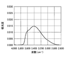
- FIG. 6 is a chart showing an example of FTIR measurement result in a sample (Sample 2) according to Example 2.
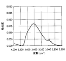
- 6 is a chart showing an example of FTIR measurement results for a sample according to Example 3 (Sample 3).
- 6 is a chart showing an example of FTIR measurement results for a sample according to Example 4 (Sample 4).
- 6 is a chart showing an example of FTIR measurement results in a sample (Sample 5) according to Comparative Example 1.
- Example 10 is a chart showing an example of FTIR measurement results for a sample (Sample 6) according to Comparative Example 2.
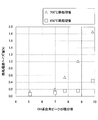
- 6 is a graph showing the relationship between the integrated value of the OH group-derived peak and the haze value after heat treatment obtained in each sample 1 to 6.
- a method for producing a glass substrate having a first layer formed on a surface thereof by a low temperature CVD method (1) preparing a glass substrate; (2) forming a first layer on the glass substrate by a low temperature CVD method; Have Wherein (2) the glass substrate after the step of, in the first peak from OH group obtained by FTIR measurements to the layer, the integral value after baseline correction in the range of wave number 2600 cm -1 ⁇ 3800 cm -1 is 9.0 or less, A method is provided in which the content of C in the first layer is 1.64 at% or less.
- low temperature CVD process is different from a high temperature CVD process such as a thermal CVD process, and a film forming process is performed under a relatively low substrate temperature condition such as 100 ° C. or lower.
- a CVD process includes, for example, a plasma CVD (PECVD) process.
- the substrate temperature may increase significantly during the pre-treatment of the substrate before the CVD process and during the CVD process. As long as there is no heating step, it is included in the “low temperature CVD process (method)”.
- high-speed low-temperature CVD process a technique for forming a target substance at a high speed by a low-temperature CVD process (hereinafter referred to as “high-speed low-temperature CVD process”) has been studied.
- high-speed low-temperature CVD process normally, a film formed by such a “high-speed low-temperature CVD process” has a problem that heat resistance is relatively poor.
- the inventors of the present application as a result of intensive studies, in a glass substrate on which a layer such as a thin film is formed by a low temperature CVD process, the peak area derived from OH groups obtained by FTIR absorbance measurement on the layer, It has been found that there is a correlation between the heat resistance of the layers. At this time, the FTIR absorbance measurement is performed on the glass substrate on which the layer is formed and the same type of glass substrate on which the layer is not formed, and the difference between the respective absorbances is taken to measure the FTIR absorbance of the layer. . Furthermore, the inventors of the present application, when the layer is formed such that the peak area derived from the OH group is a predetermined value or less, the glass substrate on which the layer having good heat resistance is formed As a result, the present invention was found.
- the glass substrate with a thin film produced by the method according to the present invention has an integrated value of peaks derived from OH groups in the wave number range of 2600 cm ⁇ 1 to 3800 cm ⁇ 1 (after baseline correction) obtained by FTIR measurement on the thin film. However, it has the characteristic that it is suppressed to 9.0 or less. That is, in the method for producing a glass substrate with a thin film according to the present invention, the content of OH groups contained in the obtained thin film is significantly suppressed.
- the content of C (carbon) contained in the first layer is characterized by being suppressed to 1.64 at% or less (note that C (carbon) is usually mixed into the thin film from the raw material side).
- the method for producing a glass substrate with a thin film according to the present invention can provide a glass substrate with a thin film having relatively good heat resistance.
- FIG. 1 schematically shows a change state when a SiO 2 thin film formed on a glass substrate is subjected to a thermal history by a conventional low-temperature CVD process.
- FIG. 1A shows a state before the glass substrate 110 with the SiO 2 thin film is heated.
- An SiO 2 thin film 120 formed by a low temperature CVD process is disposed on the glass substrate 110.
- an organometallic compound gas such as tetramethyldisiloxane is usually used as a source gas.
- the film formation temperature is relatively low (for example, about 20 ° C. to 100 ° C.)
- the OH group derived from the organic metal compound gas as a raw material is formed in the formed SiO 2 thin film 120. It is thought that 125 is taken in.
- the SiO 2 thin film 120 is formed by a high-speed film forming process, there is a possibility that a large amount of OH groups 125 are taken into the SiO 2 thin film 120 as a result of an increase in the amount of unreacted raw materials.
- the glass substrate 110 with the SiO 2 thin film 120 is still in a heated state. Therefore, holes 130 formed in the SiO 2 thin film 120 is sintered of SiO 2 thin film 120, reduced by the progress of densification, further disappears. Note that, as indicated by an arrow A in FIG. 1C, the volume of the SiO 2 thin film 120 is reduced by densification, so that the dimension of the SiO 2 thin film 120 is smaller than that of the glass substrate 110.
- the glass substrate 110 expands by heating. That is, the glass substrate 110 expands so as to extend in the direction of arrow B as shown in FIG.
- a tensile force is also applied in the direction of arrow B to the densified SiO 2 thin film 120.
- microscopic or macroscopic cracking occurs in the densified SiO 2 thin film 120.
- the content of OH groups contained in the thin film formed by the low temperature CVD process is significantly suppressed. For this reason, when the glass substrate with a thin film manufactured by the method according to the present invention is subjected to heat treatment, a reaction in which the OH group changes to water is less likely to occur. Further, since the amount of water released to the outside is reduced, the amount of vacancies formed in the thin film during the heat treatment is also reduced, and the thin film is hardly densified. As a result, even if heat treatment is performed, defects such as cracks are less likely to occur in the thin film, and it is considered that the heat resistance of the glass substrate with the thin film is improved.
- the glass substrate with a thin film produced by the method according to the present invention is characterized in that the content of C (carbon) contained in the first layer is suppressed to 1.64 at% or less. For this reason, in the glass substrate with a thin film manufactured by the method according to the present invention, the above-described phenomenon is less likely to occur, and the heat resistance of the thin film is improved.
- FIG. 2 is a flowchart schematically showing an example of a method for producing a glass substrate with a thin film according to the present invention.
- an example of a method for producing a glass substrate with a thin film according to the present invention is (1) preparing a glass substrate (step S110); (2) A step of forming a first layer on the glass substrate by a low-temperature CVD method, and the obtained glass substrate is at a peak derived from an OH group obtained by FTIR measurement on the first layer.
- the integrated value after baseline correction in the range of wave numbers 2600 cm ⁇ 1 to 3800 cm ⁇ 1 is 9.0 or less, and the C content in the first layer is 1.64 at% or less
- Step S120 Have
- the “integrated value after baseline correction” means an integrated value after correcting the baseline from raw measurement data obtained by FTIR measurement in the wave number range.
- a glass substrate for film formation is prepared.
- the dimensions and material of the glass substrate are not particularly limited.
- the glass substrate may be, for example, soda lime glass or non-alkali glass.
- the manufacturing method of the glass substrate is not particularly limited.
- the glass substrate may be manufactured by a conventionally known general method such as a float method.
- Step S120 Next, a first layer is formed on the glass substrate by a low temperature CVD method.
- the low-temperature CVD method performs film formation at a relatively low substrate temperature.
- the low temperature CVD method may be, for example, a plasma CVD (PECVD) process.
- the plasma gas may be oxygen gas, for example.
- the glass substrate prepared in step S110 described above is placed in the film formation chamber.
- a raw material gas that is a raw material of the first layer is supplied into the film forming chamber.
- the inside of the film forming chamber may be a normal pressure environment or a reduced pressure environment.
- PECVD plasma CVD
- the inside of the film formation chamber is brought into a reduced pressure environment by a reduced pressure process.
- the type of the first layer to be formed is not particularly limited.
- the first layer may be, for example, an oxide, nitride, and / or oxynitride.
- Examples of the oxide include SiO 2 , TiO 2 , ZnO, SnO, and / or Al 2 O 3 .
- Examples of the nitride include Si 3 N 4 , TiN, and AlN.
- Examples of oxynitrides include SiON and TiON.
- the source gas may include, for example, an organic metal source.
- the organometallic raw material may have, for example, a siloxane bond and / or an alkoxide bond. Further, the organometallic raw material may include at least one component selected from the group consisting of —CH 3 group, —OH group, and —H group. The organometallic raw material may include at least one component selected from the group consisting of Si, Ti, Zn, Sn, and Al. In this case, oxides, nitrides, oxynitrides, and the like of silicon, titanium, zinc, tin, and aluminum can be formed.
- the film forming process is performed so as to be 9.0 or less.
- Such control of the amount of OH groups can be performed relatively easily, for example, by controlling the amount of raw material supplied during the formation of the first layer within a predetermined range.
- the flow rate of the raw material is set to about 125 sccm / m to 250 sccm / m.
- An SiO 2 thin film having a peak derived from an integrated value of 9.0 or less can be formed.
- the integral value after baseline correction in the range of wave number 2600 cm -1 ⁇ 3800 cm -1 is preferably 7.0 or less, more preferably 5.5 or less.
- the film forming process is performed such that the C (carbon) content in the first layer is 1.64 at% or less.
- C may be detected as an impurity in the first layer after film formation even when the source gas does not contain a C component.
- the content of C derived from such impurities is expected to be about 3.2 ppm at the maximum. Therefore, unless a raw material containing a C component such as an organometallic raw material is used as a raw material for the film formation of the first layer, the above-described C (carbon) content condition (C ⁇ 1.64 at%) ) Is satisfied.
- the supply amount of such an organic metal raw material should be controlled within a predetermined range.
- the amount of C (carbon) can be controlled relatively easily.
- the content of C derived from the raw material is more preferably 1 at% or less.
- the content of C in the first layer can be measured by the ESCA method. That is, normally, since the glass substrate itself does not contain C, the value obtained by the measurement result of the ESCA analysis in the entire glass substrate with a thin film is grasped as the C content in the first layer. Can do.
- FIG. 3 shows a schematic cross-sectional view of an example of a glass substrate with a thin film according to the present invention.
- the glass substrate 300 with a thin film according to the present invention includes a glass substrate 310 and a first layer 320 formed on the surface 312 of the glass substrate 310.
- the type of the glass substrate 310 is not particularly limited.
- the glass substrate 310 may be, for example, soda lime glass or non-alkali glass.
- the first layer 320 is formed by a low temperature CVD process such as a PECVD method.
- the material of the first layer 320 is not particularly limited.
- the thin film material 300 may be, for example, an oxide, a nitride, and / or an oxynitride.
- Examples of the oxide include SiO 2 , TiO 2 , ZnO, SnO, and Al 2 O 3 .
- Examples of the nitride include SiN, TiN, and AlN.
- Examples of oxynitrides include SiON and TiON.
- a thin film glass substrate 300 the peak derived from OH group obtained by FTIR measurements on the first layer 320, the integral value after baseline correction in the range of wave number 2600 cm -1 ⁇ 3800 cm -1 is 9 0.0 or less.
- the integral value is preferably 7.0 or less, and more preferably 5.5 or less.
- the content of C derived from the raw material contained in the first layer 320 is suppressed to 1.64 at% or less.
- the content of C contained in the first layer 320 is preferably 1 at% or less.
- the glass substrate with a thin film 300 having such a feature hardly densifies the first layer 320 due to the detachment of OH groups during the heat treatment, the first layer 320 has cracks or the like. Defects are hardly generated, that is, heat resistance is significantly high.
- the glass substrate 300 with a thin film according to the present invention has a very low haze value, for example, a haze value of 0.2% or less even after being held at 650 ° C. for 10 minutes or more.
- the glass substrate with a thin film 300 according to the present invention can be applied significantly even in applications where heat treatment is applied later.
- the thickness of the first layer 320 is not particularly limited.
- the thickness of the first layer 320 may be in the range of 5 nm to 1000 nm, for example.
- a plurality of layers may be formed on the surface of the glass substrate with a thin film.
- FIG. 4 schematically shows an example of the configuration of the second glass substrate with a thin film according to the present invention.
- the second thin film-attached glass substrate 400 includes a glass substrate 410, a first layer 420 disposed on the surface 412 of the glass substrate 410, and the first layer 420. And a second layer 430 disposed thereon.
- the glass substrate 410 may be a glass substrate such as the glass substrate 310 shown in FIG.
- the first layer 420 is formed by a low temperature CVD process such as a PECVD method, for example.
- the second layer 430 is also formed by a low temperature CVD process such as PECVD.
- the first layer 420 may be a material different from that of the second layer 430.
- Each layer 420, 430 may have a thickness in the range of 5 nm to 1000 nm.
- a thin film glass substrate 400 the peak derived from OH group obtained by FTIR measurements on the first layer 420 and second layer 430, after baseline correction in the range of wave number 2600 cm -1 ⁇ 3800 cm -1
- the integral value of is not more than 9.0. That is, in the glass substrate 400 with the second thin film, the total amount of OH groups contained in the first layer 420 and the second layer 430 is significantly suppressed.
- the total content of C derived from the raw materials contained in the first layer 420 and the second layer 430 is suppressed to 1.64 at% or less.
- the first layer 420 and the second layer 430 are hardly densified due to OH group separation during the heat treatment. It will be apparent that the same effect as the glass substrate 300, that is, good heat resistance can be obtained.
- the glass substrate 400 with the second thin film it is difficult to grasp the content of C derived from the raw material contained in each of the first layer 420 and the second layer 430.
- the values obtained by the measurement results of the ESCA analysis in the entire glass substrate 400 with a thin film are included in the first layer 420 and the second layer 430. It can be grasped as the total content of C.
- the first layer 420 and the second layer 430 are both layers formed by a low temperature CVD process.
- one of the first layer 420 and the second layer 430 may be a layer formed by a method other than the low-temperature CVD process.
- the method other than the low-temperature CVD process include, but are not limited to, a physical vapor deposition method such as a sputtering method and a non-low-temperature CVD process such as a thermal CVD method.
- the second layer 430 is a layer formed by a method other than the low temperature CVD process
- the second layer 430 is assumed to contain almost no OH group.
- the first layer 420 is assumed to be the source of the peak derived from the OH group obtained by the FTIR measurement on the first layer 420 and the second layer 430.
- the value of the C amount obtained from the measurement result is used as the C component contained in the first layer 420. Can be estimated.
- the glass substrate 400 with the second thin film having such a configuration as in the case of the glass substrate 300 with the thin film described above, it is derived from the OH group obtained by the FTIR measurement on the first layer 420 and the second layer 430.
- the integrated value after baseline correction in the range of wave numbers from 2600 cm ⁇ 1 to 3800 cm ⁇ 1 is suppressed to 9.0 or less, and the amount of measured C component is suppressed to 1.64 at% or less. Thereby, it becomes possible to improve the heat resistance of the glass substrate with a thin film.
- FIG. 5 An example of a structure of the 3rd glass substrate with a thin film by this invention is shown roughly.
- the third thin film-attached glass substrate 500 includes a glass substrate 510, a first layer 520 disposed on the surface 512 of the glass substrate 510, and the first layer 520. It has the 2nd layer 530 arrange
- the glass substrate 510 may be a glass substrate such as the glass substrates 310 and 410 shown in FIG. 3 and / or FIG.
- the first layer 520 is formed by a low temperature CVD process such as a PECVD method, for example.
- the third layer 540 is also formed by a low temperature CVD process.
- the first layer 520 and the third layer 540 may be the same material or different materials.
- the second layer 530 is formed by a non-low temperature CVD process.
- the first layer 520 and the third layer 540 may each have a thickness in the range of 5 nm to 1000 nm.
- the second layer 530 may have a thickness in the range of 5 nm to 1000 nm.
- the third thin film-coated glass substrate 500 the peak derived from OH group obtained by FTIR measurements on the first layer 520 to the third layer 540, the base in the range of wave number 2600 cm -1 ⁇ 3800 cm -1
- the integrated value after line correction is 9.0 or less.
- the total content of C derived from the raw materials contained in the first layer 520 and the third layer 540 is suppressed to 1.64 at% or less.
- the total amount of OH groups contained in the first layer 520 and the third layer 540 formed by the low temperature CVD process and the total amount of C contained in both layers are significantly suppressed. Has been.
- the third glass substrate 500 with a thin film can obtain the same effect as the glass substrates 300 and 400 with a thin film, that is, good heat resistance.
- the configuration example of the glass substrate 500 with the third thin film in which only the first layer 520 and the third layer 540 are formed by the low temperature CVD process has been described.
- the configuration of the third thin film-attached glass substrate 500 is not limited to this.
- the first layer 520 may be a layer formed by a low temperature CVD process
- the second layer 530 and the third layer 540 may be layers formed by a non-low temperature CVD process.
- the second layer 530 may be a layer formed by a low temperature CVD process
- the first layer 530 and the third layer 540 may be layers formed by a non-low temperature CVD process.
- the third layer 540 may be a layer formed by a low temperature CVD process
- the first layer 520 and the second layer 530 may be layers formed by a non-low temperature CVD process.
- all of the first layer 520 to the third layer 540 may be layers formed by a low temperature CVD process.
- the number of layers is not limited to three, and the number of layers may be four or more.
- FIG. 6 schematically shows an example of a cross-sectional view of the infrared reflecting glass.
- the infrared reflection glass 600 includes a glass substrate 610 and a multilayer body 620 of a plurality of dielectric layers installed on the glass substrate 610.
- the dielectric layer stack 620 includes a first dielectric layer 630, a second dielectric layer 640, a third dielectric layer 650, a fourth dielectric layer 660, and a side closer to the glass substrate 610.
- the fifth dielectric layer 670 is stacked.
- the first stacked body 630 has a first refractive index n 1
- the second stacked body 640 has a second refractive index n 2
- the third stacked body 650 has a third refractive index. It has the rate n 3
- a fourth stack 660 has a fourth refractive index n 4 of the fifth laminate 670 has a refractive index n 5 of the fifth.
- the first refractive index n 1 of the first stacked body 630 is larger than the second refractive index n 2 of the second stacked body 640
- the third refractive index n of the third stacked body 650. 3 is larger than the second refractive index n 2 of the second stacked body 640 and the fourth refractive index n 4 of the fourth stacked body 660
- the fifth refractive index n 5 of the fifth stacked body 670 Is larger than the fourth refractive index n 4 of the fourth stacked body 660.
- the first dielectric layer 630, the third dielectric layer 650, and / or the fifth dielectric layer 670 may be, for example, a TiO 2 layer. Further, the second dielectric layer 640 and / or the fourth dielectric layer 660 may be, for example, a SiO 2 layer.
- first dielectric layer 630, the third dielectric layer 650, and the fifth dielectric layer 670 may be the same layer, and the second dielectric layer 640 and the fourth dielectric layer.
- Layer 660 may be the same layer.
- a laminated body 620 composed of a total of five layers is disposed on the glass substrate 610.
- the stacked body 620 may include six or more layers.
- the infrared reflection glass 600 having such a configuration exhibits a high reflectance with respect to light in the infrared region.
- the infrared reflection glass 600 includes a glass substrate with a thin film according to the present invention.
- the glass substrate 610 of the infrared reflecting glass 600 corresponds to the glass substrate 310 of the glass substrate with a thin film 300 according to the present invention shown in FIG. 3, and the first dielectric layers 630 to 5 of the infrared reflecting glass 600 are used.
- Any one of the dielectric layers 670 may be the first layer 320 of the glass substrate with a thin film 300 according to the present invention shown in FIG.
- the glass substrate 610 of the infrared reflective glass 600 corresponds to the glass substrate 410 of the second thin film-coated glass substrate 400 according to the present invention shown in FIG. 4, and the first dielectric of the infrared reflective glass 600.
- Two consecutive layers out of the layers 630 to 670 may correspond to the first layer 420 to the second layer 430 of the glass substrate 400 with the second thin film shown in FIG. .
- the glass substrate 610 of the infrared reflecting glass 600 corresponds to the glass substrate 510 of the third glass substrate 500 with a thin film according to the present invention shown in FIG.
- Three consecutive layers out of the layers 630 to 670 may correspond to the first layer 520 to the third layer 540 of the glass substrate 500 with the third thin film shown in FIG. .
- the infrared reflective glass 600 includes such a glass substrate with a thin film according to the present invention, the heat resistance of the infrared reflective glass 600 can be increased. Therefore, the infrared reflective glass 600 can be heat-treated, for example, for bending.
- FIG. 7 schematically shows an example of a cross-sectional view of the visible light antireflection glass.
- the visible light antireflection glass 700 is installed on the glass substrate 710, the first laminated body 730 installed on the glass substrate 710, and the first laminated body 730.
- a second stacked body 760 is shown in FIG. 7, the visible light antireflection glass 700 is installed on the glass substrate 710, the first laminated body 730 installed on the glass substrate 710, and the first laminated body 730.
- a second stacked body 760 is shown in FIG. 7, the visible light antireflection glass 700 is installed on the glass substrate 710, the first laminated body 730 installed on the glass substrate 710, and the first laminated body 730.
- a second stacked body 760 is shown in FIG. 7, the visible light antireflection glass 700 is installed on the glass substrate 710, the first laminated body 730 installed on the glass substrate 710, and the first laminated body 730.
- a second stacked body 760 is shown in FIG. 7, the visible light antireflection glass 700 is installed on the glass substrate 710, the first laminated body 730 installed
- the first laminated body 730 is formed by laminating a first dielectric layer 740 having a first refractive index n 1 and a second dielectric layer 745 having a second refractive index n 2 in this order. Consists of.
- the first refractive index n 1 of the first dielectric layer 740 is greater than the second refractive index n 2 of the second dielectric layer 745.
- the first dielectric layer 740 may be, for example, a TiO 2 layer
- the second dielectric layer 745 may be, for example, an SiO 2 layer.
- the second stacked body 760 has a configuration similar to that of the first stacked body 730. That is, the second stacked body 760 includes a third dielectric layer 770 having a third refractive index n 3 and a fourth dielectric layer 775 having a fourth refractive index n 4 stacked in this order. It is constituted by doing.
- the third refractive index n 3 of the third dielectric layer 770 is greater than the fourth refractive index n 4 of the fourth dielectric layer 775.
- the third dielectric layer 770 may be, for example, a TiO 2 layer
- the fourth dielectric layer 775 may be, for example, a SiO 2 layer.
- first stacked body 730 and the second stacked body 760 may have the same configuration.
- two laminated bodies 730 and 760 are installed on the glass substrate 710.
- the visible light antireflection glass 700 having such a configuration exhibits a low reflectance with respect to visible light.
- the visible light antireflection glass 700 includes a glass substrate with a thin film according to the present invention.
- the glass substrate 710 of the visible light antireflection glass 700 corresponds to the glass substrate 310 of the glass substrate 300 with a thin film according to the present invention shown in FIG. 3, and the first dielectric layers 740 to ⁇ Any one of the fourth dielectric layers 775 may be the first layer 320 of the glass substrate with a thin film 300 according to the present invention shown in FIG.
- the glass substrate 710 of the visible light antireflection glass 700 corresponds to the glass substrate 410 of the second thin film-coated glass substrate 400 according to the present invention shown in FIG.
- Any two of the dielectric layers 740 to 775 correspond to the first layer 420 to the second layer 430 of the glass substrate 400 with the second thin film shown in FIG. Also good.
- the glass substrate 710 of the visible light antireflection glass 700 corresponds to the glass substrate 510 of the third thin film-coated glass substrate 500 according to the present invention shown in FIG.
- Any three of the dielectric layers 740 to 750 correspond to the first layer 520 to the third layer 540 of the glass substrate 500 with the third thin film shown in FIG. Also good.
- the visible light antireflection glass 700 includes such a glass substrate with a thin film according to the present invention, the heat resistance of the visible light antireflection glass 700 can be increased. Therefore, the visible light antireflection glass 700 can be heat-treated, for example, for bending.
- FIG. 8 schematically shows an example of a cross-sectional view of Low-E glass.
- the Low-E glass 800 includes a glass substrate 810, a silver layer 830, and an upper layer 850 disposed on the top of the Low-E glass 800.
- the silver layer 830 is disposed between the lower first dielectric layer 820 and the upper second dielectric layer 840.
- the upper layer 850 is usually made of a dielectric layer such as SiO 2 and has a role of suppressing reflection of visible light.
- the Low-E glass 800 includes a glass substrate with a thin film according to the present invention.
- the glass substrate 810 and the upper layer 850 of the Low-E glass 800 may be the glass substrate 310 and the first layer 320 of the glass substrate with a thin film 300 according to the present invention shown in FIG.
- the glass substrate 810 and the upper layer 850 of the Low-E glass 800 are respectively the glass substrate 410 and the second layer 430 of the glass substrate 400 with the second thin film according to the present invention shown in FIG. Also good.
- the first layer 420 of the second glass substrate with a thin film 400 may correspond to the first dielectric layer 820 or the second dielectric layer 840.
- the glass substrate 810 and the upper layer 850 of the Low-E glass 800 are the glass substrate 510 and the third layer 540 of the glass substrate 500 with the third thin film according to the present invention shown in FIG. Also good.
- the first layer 520 of the glass substrate 500 with the third thin film corresponds to the first dielectric layer 820
- the second layer 530 of the glass substrate 500 with the third thin film is the second dielectric layer. It may correspond to the body layer 840.
- the Low-E glass 800 includes such a glass substrate with a thin film according to the present invention, the heat resistance of the Low-E glass 800 can be improved. Therefore, the Low-E glass 800 can be heat-treated, for example, for bending.
- Low-E glass 800 having the configuration shown in FIG. 8 is merely an example, and the Low-E glass may have other configurations.
- FIG. 9 schematically shows an example of a cross-sectional view of Low-E glass having another configuration.
- the Low-E glass 900 includes a glass substrate 910, a bottom layer 920 disposed on the glass substrate 910, and a first dielectric disposed on the bottom layer 920.
- a layer 930, a silver layer 940 disposed on the first dielectric layer 930, and a second dielectric layer 950 disposed on the silver layer 940 are stacked in this order. Is done.
- the bottom layer 920 has a role of suppressing alkali metal diffusion from the glass substrate 920 toward the silver layer 940.
- the bottom layer 920 is composed of a dielectric layer such as SiO 2 .
- the Low-E glass 900 includes a glass substrate with a thin film according to the present invention.
- the glass substrate 910 and the bottom layer 920 of the Low-E glass 900 may be the glass substrate 310 and the first layer 320 of the glass substrate with a thin film 300 according to the present invention shown in FIG.
- the heat resistance of the Low-E glass 900 can be increased.
- the Low-E glass 900 can be heat-treated, for example, for bending.
- the glass substrate 910 and the bottom layer 920 of the Low-E glass 900 are the glass substrate 410 and the first layer 420 of the second thin film-coated glass substrate 400 shown in FIG. 4 according to the present invention, respectively. Also good.
- the second layer 430 of the second glass substrate with a thin film 400 may correspond to the first dielectric layer 930 or the second dielectric layer 950.
- the glass substrate 910 and the bottom layer 920 of the Low-E glass 900 are the glass substrate 510 and the first layer 520 of the third thin film-coated glass substrate 500 shown in FIG. Also good.
- the second layer 30 of the third glass substrate with a thin film 500 corresponds to the first dielectric layer 930
- the third layer 540 of the third glass substrate with a thin film 500 is a second dielectric layer. It may correspond to the body layer 950.
- Example 1 A SiO 2 thin film was formed on the substrate by the following method to prepare Sample 1 and its characteristics were evaluated.
- a PECVD apparatus was used for forming the SiO 2 thin film.
- the plasma gas was oxygen gas (flow rate 2000 sccm / m), and the plasma power was 20 kW / m.
- Tetramethyldisiloxane was used as the source gas.
- the flow rate of the source gas was 250 sccm / m.
- a soda-lime glass substrate having a length of 300 mm, a width of 300 mm, and a thickness of 2 mm was used as the substrate.
- the substrate is not heated during film formation.
- a SiO 2 thin film having a thickness of about 226 nm was formed on the substrate by the PECVD process.
- the deposition rate calculated from the deposition time and the thickness of the SiO 2 thin film was 226 nm ⁇ m / min.
- FTIR absorbance measurement was performed on the SiO 2 thin film of Sample 1 obtained. At this time, FTIR absorbance measurement is performed on the same kind of glass substrate as that used for Sample 1 and Sample 1, and the difference in absorbance between the two is taken to measure the FTIR absorbance of the SiO 2 thin film.
- an FTIR measuring device Nicolet 6700 FT-IR: manufactured by Thermo Scientific
- FIG. 10 shows a partially enlarged view of the FTIR measurement result.
- this figure has shown the data after correct
- Baseline correction was performed by auto-baseline correction using software attached to the FTIR measurement device (OMNIC software: manufactured by Thermo Scientific).
- OMNIC software manufactured by Thermo Scientific
- an operation of approximating a baseline inclination or waviness that occurs in a spectrum waveform due to the light scattering of a sample by a polynomial curve is performed.
- the C content contained in the SiO 2 thin film of Sample 1 was measured.
- the C content was measured with an ESCA apparatus (PHI 5000 VersaProbe II: manufactured by ULVAC-PHI).
- the C content contained in the SiO 2 thin film was 0.55 at%.
- the heat resistance evaluation was performed by measuring the haze value after heat treatment of Sample 1.
- haze is one of the indicators of the transparency of the sample, and is used when expressing the turbidity (cloudiness) of the sample.
- the turbidity of the sample increases, thereby increasing the haze value. Therefore, the heat resistance of the sample can be evaluated by measuring the haze value.
- the heat treatment was performed by holding Sample 1 at 650 ° C. and 700 ° C. for 17 minutes in the air.
- the haze value of Sample 1 was measured with a haze meter (Haze Meter HZ-2: manufactured by Suga Test Instruments Co., Ltd.).
- the haze value after heat treatment at 700 ° C. was 1.01, and it was found that the turbidity of Sample 1 after heat treatment at 700 ° C. was low. Thus, it was confirmed that Sample 1 has good heat resistance even after heat treatment at 700 ° C.
- Example 2 By the same method as in Example 1, a SiO 2 thin film was formed on the substrate to produce Sample 2, and the characteristics were evaluated. However, in Example 2, the plasma power was 25 kW / m, the deposition rate was 221 nm ⁇ m / min, and the thickness of the SiO 2 thin film was 221 nm. Other conditions are the same as in the first embodiment.
- FIG. 11 shows an enlarged view (after baseline correction) of the FTIR measurement result of the sample 2 on the SiO 2 thin film.
- the peak integrated value was 7.7.
- the C content was 0.21 at%.
- the haze value of Sample 2 after the heat treatment at 650 ° C. was 0.16. Further, in visual observation, no abnormalities such as cracks were observed in the SiO 2 thin film of Sample 2. From this result, it was confirmed that Sample 2 had very good heat resistance with few defects such as cracks after heat treatment at 650 ° C. Moreover, the haze value of the sample 2 of heat processing at 700 degreeC was 0.55, and it turned out that the turbidity of the sample 2 after heat processing at 700 degreeC is low. Thus, it was confirmed that Sample 2 had good heat resistance even after heat treatment at 700 ° C.
- Example 2 In the column of “Example 2” in Table 1 above, typical film forming conditions of Sample 2, the integrated value of peaks derived from OH groups, haze values after heat treatment at 650 ° C. and 700 ° C., and C content The amount is shown together.
- Example 3 A sample 3 was prepared by forming a SiO 2 thin film on the substrate by the same method as in Example 1, and the characteristics thereof were evaluated. However, in Example 3, the plasma power is 25 kW / m, the flow rate of the source gas is 187.5 sccm / m, the flow rate of the plasma oxygen gas is 1500 sccm / m, and the deposition rate is 151 nm ⁇ m / min. The thickness of the SiO 2 thin film was 216 nm. Other conditions are the same as in the first embodiment.
- FIG. 12 shows an enlarged view (after baseline correction) of the FTIR measurement result of the sample 3 on the SiO 2 thin film.
- the peak integrated value was 7.0.
- the C content was 0.24 at%.
- the haze value of Sample 3 after the heat treatment at 650 ° C. was 0.10. Further, in visual observation, no abnormalities such as cracks were observed in the SiO 2 thin film of Sample 3. From this result, it was confirmed that the sample 3 had very good heat resistance with few defects such as cracks after heat treatment at 650 ° C. Moreover, the haze value of the sample 3 of the heat processing at 700 degreeC is 0.20, and it turned out that the turbidity of the sample 3 after the heat processing at 700 degreeC is also very low. Further, in visual observation, no abnormalities such as cracks were observed in the SiO 2 thin film of Sample 2. From this result, it was confirmed that Sample 3 has very good heat resistance with almost no defects such as cracks even after heat treatment at 700 ° C.
- Example 3 In the column of “Example 3” in Table 1 above, typical film forming conditions of Sample 3, the integrated value of peaks derived from OH groups, haze values after heat treatment at 650 ° C. and 700 ° C., and C content The amount is shown together.
- Example 4 By the same method as in Example 1, a SiO 2 thin film was formed on the substrate to prepare Sample 4, and the characteristics thereof were evaluated. However, in Example 4, the plasma power is 25 kW / m, the flow rate of the source gas is 125 sccm / m, the flow rate of the plasma oxygen gas is 1000 sccm / m, the deposition rate is 90 nm ⁇ m / min, and SiO 2 The thickness of the thin film was 224 nm. Other conditions are the same as in the first embodiment.
- FIG. 13 shows an enlarged view (after baseline correction) of the FTIR measurement result of the sample 4 on the SiO 2 thin film.
- the peak integrated value was 5.1.
- the C content was 0.24 at%.
- the haze value of Sample 4 after the heat treatment at 650 ° C. was 0.06. Further, in visual observation, no abnormalities such as cracks were observed in the SiO 2 thin film of Sample 4. From this result, it was confirmed that the sample 4 had very good heat resistance with few defects such as cracks after heat treatment at 650 ° C. Moreover, the haze value of the sample 4 of the heat processing at 700 degreeC is 0.13, It turned out that the turbidity of the sample 4 after 700 degreeC heat processing is also very low. Further, in visual observation, no abnormalities such as cracks were observed in the SiO 2 thin film of Sample 4. From this result, it was confirmed that the sample 4 had extremely good heat resistance with few defects such as cracks even after heat treatment at 700 ° C.
- Example 4 In the column of “Example 4” in Table 1 above, typical film forming conditions of Sample 4, the integrated value of peaks derived from OH groups, haze values after heat treatment at 650 ° C. and 700 ° C., and C content The amount is shown together.
- Comparative Example 1 A sample 5 was prepared by forming a SiO 2 thin film on the substrate by the same method as in Example 1, and the characteristics thereof were evaluated.
- the plasma power is 10 kW / m
- the raw material gas flow rate is 100 sccm
- the plasma oxygen gas flow rate is 800 sccm
- the deposition rate is 252 nm ⁇ m / min
- the thickness of the SiO 2 thin film was 252 nm.
- Other conditions are the same as in the first embodiment.
- FIG. 14 shows an enlarged view (after baseline correction) of the FTIR measurement result of the sample 5 on the SiO 2 thin film.
- the peak integrated value was 8.1.
- the C content was 4.30 at%.
- the haze values after heat treatment at 650 ° C. and 700 ° C. were 0.61 and 1.92, respectively. From this, it was found that the turbidity of Sample 5 after the heat treatment was remarkably increased. Further, in the visual observation, the SiO 2 thin film sample 5 after heat treatment at 650 ° C. and 700 ° C., was observed that a number of cracks are generated. From this result, it was confirmed that Sample 5 did not show good heat resistance.
- Comparative Example 2 A sample 6 was prepared by forming a SiO 2 thin film on the substrate by the same method as in Comparative Example 1, and the characteristics thereof were evaluated. However, in Comparative Example 2, the plasma power was 15 kW / m, the deposition rate was 240 nm ⁇ m / min, and the thickness of the SiO 2 thin film was 240 nm. Other conditions are the same as in Comparative Example 1.
- FIG. 1 An enlarged view (after baseline correction) of the FTIR measurement result of the sample 6 on the SiO 2 thin film is shown in FIG.
- the peak integrated value was 9.8.
- the C content was 1.64 at%.
- the haze values after heat treatment at 650 ° C. and 700 ° C. were 0.45 and 1.86, respectively, and it was found that the turbidity of Sample 6 after heat treatment was large. Further, in the visual observation, the SiO 2 thin film sample 6 after thermal treatment at 650 ° C. and 700 ° C., was observed that a number of cracks are generated. From this result, it was confirmed that Sample 6 did not show good heat resistance.
- FIG. 16 shows the relationship between the integrated value of the OH group-derived peak obtained in each sample 1 to 6 and the haze value after heat treatment at 650 ° C. and 700 ° C., respectively. Sample 5 is not plotted because the C content exceeds 1.64 at%.
- FIG. 16 shows that in the case of heat treatment at 650 ° C., when the integrated value of the OH group-derived peak obtained by FTIR measurement exceeds about 9.0, the haze value after heat treatment of the sample is remarkably increased. This result shows that when the integrated value of the peak derived from the OH group exceeds about 9.0, the heat resistance of the sample is significantly lowered.
- the present invention can be used for a film forming technique using a CVD process.
Landscapes
- Chemical & Material Sciences (AREA)
- Organic Chemistry (AREA)
- General Chemical & Material Sciences (AREA)
- Engineering & Computer Science (AREA)
- Chemical Kinetics & Catalysis (AREA)
- Materials Engineering (AREA)
- Physics & Mathematics (AREA)
- Geochemistry & Mineralogy (AREA)
- Life Sciences & Earth Sciences (AREA)
- General Physics & Mathematics (AREA)
- Optics & Photonics (AREA)
- Mechanical Engineering (AREA)
- Inorganic Chemistry (AREA)
- Metallurgy (AREA)
- Health & Medical Sciences (AREA)
- Toxicology (AREA)
- Surface Treatment Of Glass (AREA)
- Chemical Vapour Deposition (AREA)
- Laminated Bodies (AREA)
Abstract
低温CVD法により表面に第1の層が成膜されたガラス基板を製造する方法であって、(1)ガラス基板を準備するステップと、(2)低温CVD法により、前記ガラス基板に第1の層を成膜するステップと、を有し、前記(2)のステップ後のガラス基板は、前記第1の層へのFTIR測定によって得られるOH基由来のピークにおける、波数2600cm-1~3800cm-1の範囲のベースライン補正後の積分値が、9.0以下であり、前記第1の層におけるCの含有量は、1.64at%以下であることを特徴とする方法。
Description
本発明は、表面に1または2以上の層が低温CVDプロセスにより成膜されたガラス基板を製造する方法、および表面に1または2以上の層が低温CVDプロセスにより成膜されたガラス基板に関する。
CVD(化学気相成膜)プロセスは、原料ガスの化学反応を利用して、目的物質を基板に成膜する技術である。CVDプロセスでは、基板表面が凹凸を有する場合であっても、比較的均一に膜を成膜することができるという特徴を有し、これまでに各種分野において、幅広く利用されている。
最近では、一度に多量の原料を供給することにより、より高速に、成膜処理を実施することが検討されている。例えば、非特許文献1には、低温でのCVDプロセスの一種である、プラズマCVD(PECVD)プロセスにより、ガラス基板上に、SiO2膜を高速で成膜する技術が記載されている。
AIMCAL Techinical Conference,2011,presentation title 「High Quality High Rate Coatings by Linear PECVD」
前述のように、近年、特に低温でのCVDプロセスにより、ガラス基板上に目的物質を高速で成膜する技術(以下、「高速低温CVDプロセス」という)が検討されている。
しかしながら、本願発明者らは、このような「高速低温CVDプロセス」で成膜された層は、比較的耐熱性が悪いという問題を見出した。例えば、前述の非特許文献1に記載の方法で成膜されたSiO2膜を有するガラス基板では、650℃~700℃程度に加熱すると、SiO2膜に多数のクラックが生じることが認められている。
一方、ガラス産業分野では、「高速低温CVDプロセス」により表面に薄膜のような層が形成されたガラス基板に対して、後工程において、強化および変形させるような熱処理を行うケースは、極めて頻繁に存在し得ると考えられる。従って、「高速低温CVDプロセス」で成膜された層を有するガラス基板の耐熱性が問題となる場面は、今後、顕著化する可能性がある。
このとき、低温CVDプロセスにより成膜された層は、有機金属原料由来の不純物の影響により、耐擦傷性などの特性が低下するということがよく知られている。従って、前述の耐熱性についても、層中に残存する不純物の影響によるものと考えられる。しかしながら、耐熱性に関与する不純物成分について報告された例はなく、耐熱性を向上させる指針についても明らかになっていない。
本発明は、このような問題に鑑みなされたものであり、本発明では、低温CVDプロセスにより、表面に比較的良好な耐熱性を有する層が成膜されたガラス基板を製造する方法を提供することを目的とする。また、本発明では、低温CVDプロセスにより、表面に比較的良好な耐熱性を有する層が成膜されたガラス基板を提供することを目的とする。
本発明では、低温CVD法により表面に第1の層が成膜されたガラス基板を製造する方法であって、
(1)ガラス基板を準備するステップと、
(2)低温CVD法により、前記ガラス基板に第1の層を成膜するステップと、
を有し、
前記(2)のステップ後のガラス基板は、前記第1の層へのFTIR測定によって得られるOH基由来のピークにおける、波数2600cm-1~3800cm-1の範囲のベースライン補正後の積分値が、9.0以下であり、
前記第1の層におけるCの含有量は、1.64at%以下であることを特徴とする方法が提供される。
(1)ガラス基板を準備するステップと、
(2)低温CVD法により、前記ガラス基板に第1の層を成膜するステップと、
を有し、
前記(2)のステップ後のガラス基板は、前記第1の層へのFTIR測定によって得られるOH基由来のピークにおける、波数2600cm-1~3800cm-1の範囲のベースライン補正後の積分値が、9.0以下であり、
前記第1の層におけるCの含有量は、1.64at%以下であることを特徴とする方法が提供される。
ここで、本発明による方法において、前記(2)のステップは、前記ガラス基板に有機金属原料を供給するステップを有しても良い。
また、本発明による方法において、前記有機金属原料は、Si、Ti、Zn、Sn、およびAlからなる群から選定された少なくとも一つの成分を含んでも良い。
また、本発明による方法において、前記有機金属原料は、-CH3基、-OH基、および-H基からなる群から選定された少なくとも一つの成分を含んでも良い。
また、本発明による方法において、前記第1の層は、酸化物、窒化物、および/または酸窒化物であっても良い。
また、本発明による方法において、前記(2)のステップは、50nm・m/分~400nm・m/分の範囲の成膜速度で実施されても良い。
また、本発明による方法において、前記低温CVD法は、PECVD法であっても良い。
また、本発明による方法は、さらに、
(3)低温CVD法以外の方法により、前記ガラス基板に第2の層を成膜するステップ
を有しても良い。
(3)低温CVD法以外の方法により、前記ガラス基板に第2の層を成膜するステップ
を有しても良い。
この場合、前記(3)のステップは、前記(2)のステップの前または後に実施されても良い。
また、本発明による方法は、さらに、前記(2)のステップの後に、
(4)低温CVD法により、前記ガラス基板に第3の層を成膜するステップ
を有しても良い。
(4)低温CVD法により、前記ガラス基板に第3の層を成膜するステップ
を有しても良い。
この場合、前記(4)のステップ後のガラス基板は、前記第1~第3の層へのFTIR測定によって得られるOH基由来のピークにおける、波数2600cm-1~3800cm-1の範囲のベースライン補正後の積分値が、9.0以下であっても良い。
また、本発明では、低温CVD法により表面に第1の層が成膜されたガラス基板であって、
前記第1の層へのFTIR測定によって得られるOH基由来のピークにおける、波数2600cm-1~3800cm-1の範囲のベースライン補正後の積分値が、9.0以下であり、前記第1の層中のCの含有量は、1.64at%以下であることを特徴とするガラス基板が提供される。
前記第1の層へのFTIR測定によって得られるOH基由来のピークにおける、波数2600cm-1~3800cm-1の範囲のベースライン補正後の積分値が、9.0以下であり、前記第1の層中のCの含有量は、1.64at%以下であることを特徴とするガラス基板が提供される。
ここで、本発明によるガラス基板において、前記第1の層は、酸化物、窒化物、および/または酸窒化物であっても良い。
また、本発明によるガラス基板において、前記第1の層は、SiO2、TiO2、ZnO、SnO、およびAl2O3からなる群から選定された少なくとも一つを含んでも良い。
また、本発明によるガラス基板において、前記第1の層は、SiN、TiN、およびAlNからなる群から選定された少なくとも一つを含んでも良い。
また、本発明によるガラス基板は、650℃での熱処理後に、0.2%以下のヘイズ率を有しても良い。
また、本発明によるガラス基板において、前記低温CVD法は、PECVD法であっても良い。
また、本発明によるガラス基板において、当該ガラス基板の前記表面には、さらに、
低温CVD法以外の方法により成膜された第2の層が配置されても良い。
低温CVD法以外の方法により成膜された第2の層が配置されても良い。
この場合、
前記第2の層は、前記第1の層の上部に配置され、または
前記第1の層は、前記第2の層の上部に配置されても良い。
前記第2の層は、前記第1の層の上部に配置され、または
前記第1の層は、前記第2の層の上部に配置されても良い。
また、本発明によるガラス基板において、当該ガラス基板の前記表面には、さらに、
低温CVD法により成膜された第3の層が配置されても良い。
低温CVD法により成膜された第3の層が配置されても良い。
さらに、本発明では、ガラス基板上に、屈折率の異なる2層以上の誘電体層の交互組み合わせ構造を有する赤外反射ガラスであって、
前記ガラス基板は、前述の特徴を有するガラス基板であり、前記誘電体層の一つは、前記第1の層に相当することを特徴とする赤外反射ガラスが提供される。
前記ガラス基板は、前述の特徴を有するガラス基板であり、前記誘電体層の一つは、前記第1の層に相当することを特徴とする赤外反射ガラスが提供される。
さらに、本発明では、ガラス基板上に、屈折率の異なる2層以上の誘電体層の交互組み合わせ構造を有する反射防止ガラスであって、
前記ガラス基板は、前述の特徴を有するガラス基板であり、前記誘電体層の一つは、前記第1の層に相当することを特徴とする反射防止ガラスが提供される。
前記ガラス基板は、前述の特徴を有するガラス基板であり、前記誘電体層の一つは、前記第1の層に相当することを特徴とする反射防止ガラスが提供される。
さらに、本発明では、ガラス基板の直上に設置された誘電体からなる底部層と、該底部層の上部に配置された2つの酸化亜鉛層の間に設置された銀を含む層と、を有するLow-Eガラスであって、
前記ガラス基板は、前述の特徴を有するガラス基板であり、前記底部層は、前記第1の層に相当することを特徴とするLow-Eガラスが提供される。
前記ガラス基板は、前述の特徴を有するガラス基板であり、前記底部層は、前記第1の層に相当することを特徴とするLow-Eガラスが提供される。
さらに、本発明では、ガラス基板上に配置された2つの誘電体層の間に設置された銀を含む層と、前記2つの誘電体層の上部に配置された屈折率の異なる誘電体からなる上部層とを有するLow-Eガラスであって、
前記ガラス基板は、前述の特徴を有するガラス基板であり、前記上部層は、前記第1の層に相当することを特徴とするLow-Eガラスが提供される。
前記ガラス基板は、前述の特徴を有するガラス基板であり、前記上部層は、前記第1の層に相当することを特徴とするLow-Eガラスが提供される。
本発明では、低温CVDプロセスにより、表面に比較的良好な耐熱性を有する層が成膜されたガラス基板を製造する方法を提供することができる。また、本発明では、低温CVDプロセスにより、表面に比較的良好な耐熱性を有する層が成膜されたガラス基板を提供することができる。
以下、図面を参照して、本発明について説明する。
(本発明による薄膜付きガラス基板を製造する方法について)
本発明では、
低温CVD法により表面に第1の層が成膜されたガラス基板を製造する方法であって、
(1)ガラス基板を準備するステップと、
(2)低温CVD法により、前記ガラス基板に第1の層を成膜するステップと、
を有し、
前記(2)のステップ後のガラス基板は、前記第1の層へのFTIR測定によって得られるOH基由来のピークにおける、波数2600cm-1~3800cm-1の範囲のベースライン補正後の積分値が、9.0以下であり、
前記第1の層におけるCの含有量は、1.64at%以下であることを特徴とする方法が提供される。
本発明では、
低温CVD法により表面に第1の層が成膜されたガラス基板を製造する方法であって、
(1)ガラス基板を準備するステップと、
(2)低温CVD法により、前記ガラス基板に第1の層を成膜するステップと、
を有し、
前記(2)のステップ後のガラス基板は、前記第1の層へのFTIR測定によって得られるOH基由来のピークにおける、波数2600cm-1~3800cm-1の範囲のベースライン補正後の積分値が、9.0以下であり、
前記第1の層におけるCの含有量は、1.64at%以下であることを特徴とする方法が提供される。
なお、本願において、「低温CVDプロセス(法)」とは、熱CVDプロセスのような高温CVDプロセスとは異なり、例えば100℃以下のような、比較的低い基板温度条件下で成膜処理が実施されるCVDプロセスを意味する。「低温CVDプロセス(法)」には、例えば、プラズマCVD(PECVD)プロセス等が含まれる。
なお、CVDプロセスの前の基板の前処理、およびCVDプロセス中に、基板温度が結果的に大きく上昇する場合もあり得るが、そのような場合も、400℃を超える温度までの「積極的な」加熱工程を有さない限り、「低温CVDプロセス(法)」に含まれる。
前述のように、低温CVDプロセスにより、目的物質を高速で成膜する技術(以下、「高速低温CVDプロセス」という)が検討されている。しかしながら、後述するように、通常、このような「高速低温CVDプロセス」で成膜された膜は、比較的耐熱性が悪いという問題がある。
本願の発明者らは、鋭意検討の結果、低温CVDプロセスにより、薄膜のような層が成膜されたガラス基板において、前記層へのFTIR吸光度測定により得られるOH基由来のピークの面積と、層の耐熱性との間に、相関が存在することを見出した。このとき、層が成膜されたガラス基板および層が成膜されていない同種のガラス基板へのFTIR吸光度測定を行い、それぞれの吸光度の差分をとることで、層のFTIR吸光度を測定している。さらに、本願の発明者らは、このOH基由来のピーク面積を所定の値以下となるようにして層の成膜を行った場合、良好な耐熱性を有する層が成膜されたガラス基板が得られることを見出し、本願発明に至った。
すなわち、本発明による方法で製造された薄膜付きガラス基板は、薄膜へのFTIR測定によって得られる、波数2600cm-1~3800cm-1の範囲のOH基由来のピークの積分値(ベースライン補正後)が、9.0以下に抑制されるという特徴を有する。すなわち、本発明による薄膜付きガラス基板を製造する方法では、得られる薄膜中に含まれるOH基の含有量は、有意に抑制されている。
また、本発明による方法で製造された薄膜付きガラス基板では、第1の層中に含まれるC(カーボン)の含有量は、1.64at%以下に抑制されているという特徴を有する(なお、C(カーボン)は、通常の場合、原料側から薄膜中に混入する)。
この場合、後述するように、薄膜付きガラス基板の耐熱性が有意に向上するという効果が得られる。
従って、本発明による薄膜付きガラス基板を製造する方法では、比較的良好な耐熱性を有する薄膜付きガラス基板を提供することが可能になる。
ここで、図1を参照して、本発明による方法によって製造される薄膜付きガラス基板が、比較的良好な耐熱性を有する理由について考察する。
図1には、従来の低温CVDプロセスによって、ガラス基板上に成膜されたSiO2薄膜が熱履歴を受けた際の変化の様子を模式的に示す。
図1(a)には、SiO2薄膜付きガラス基板110が加熱される前の状態が示されている。
ガラス基板110上には、低温CVDプロセスによって成膜されたSiO2薄膜120が配置されている。なお、低温CVDプロセスによりSiO2薄膜120を成膜する際には、通常、原料ガスとして、テトラメチルジシロキサン等の有機金属化合物ガスが使用される。
ここで、低温CVDプロセスでは、成膜温度が比較的低いため(例えば、20℃~100℃程度)、成膜されたSiO2薄膜120内には、原料である有機金属化合物ガス由来のOH基125が取り込まれていると考えられる。特に、SiO2薄膜120が高速成膜処理によって形成された場合、SiO2薄膜120内には、未反応原料の量が増加する結果、多量のOH基125が取り込まれている可能性がある。
このようなSiO2薄膜120付きガラス基板110を加熱した場合、図1(b)に示すように、SiO2薄膜120内に含まれるOH基125から水分(H2O)が生成する。この水分は、SiO2薄膜120から外部に放出される。そのため、加熱されたSiO2薄膜120内のOH基125の存在位置には、多数の空孔130が形成される。
ここで、SiO2薄膜120付きガラス基板110は、依然として加熱された状態にある。そのため、SiO2薄膜120内に形成された空孔130は、SiO2薄膜120の焼結、緻密化の進展によって減少し、さらには消滅する。なお、図1(c)の矢印Aに示すように、緻密化により、SiO2薄膜120の体積は縮小するため、SiO2薄膜120の寸法は、ガラス基板110よりも小さくなる。
一方、ガラス基板110は、加熱により膨脹する。すなわち、ガラス基板110は、加熱中、図1(c)に示すように、矢印Bの方向に伸びるように膨脹する。このような、ガラス基板110の矢印Bの方向の膨脹により、緻密化したSiO2薄膜120にも、矢印Bの方向に、引っ張り力が加わる。これにより、緻密化したSiO2薄膜120には、微視的または巨視的なワレが生じる。
その結果、熱処理後には、図1(d)に示すように、緻密化されたSiO2薄膜120に、クラック140等の欠陥が形成されるものと考えられる。
これに対して、本発明では、低温CVDプロセスによって形成された薄膜中に含まれるOH基の含有量が、有意に抑制されている。このため、本発明による方法により製造された薄膜付きガラス基板は、熱処理を実施した際に、OH基が水に変化する反応が生じ難くなる。また、外部放出される水の量が少なくなるため、熱処理中に薄膜内に形成される空孔の量も少なくなり、薄膜の緻密化が生じ難くなる。その結果、熱処理を実施しても、薄膜にクラック等の欠陥が生じ難くなり、薄膜付きガラス基板の耐熱性が向上するものと考えられる。
なお、図1に示した挙動は、現時点で、実験結果から本願発明者らが考察したモデルに過ぎない。従って、その他の機構により、本発明による方法により製造された薄膜付きガラス基板の耐熱性が改善されている可能性もあることに留意する必要がある。
また、図1を用いた前述のモデルでは、主として、薄膜中に含まれるOH基の影響に着目したが、薄膜中にC(カーボン)成分が含まれる場合も、同様に考えることができる。
すなわち、薄膜中に、例えば原料由来のC成分が存在する場合、そのようなC成分は、例えば-CH3基のような、H原子と結合した状態で存在する可能性が高い。従って、第1の層中に、このような原料由来のC成分が存在する場合、前述のOH基の場合と同様、熱処理の際にC成分が水分および炭酸ガスとなり、薄膜中から離脱する。また、これにより生じた空孔が結合して、薄膜が緻密化してしまう。その結果、熱処理後に、薄膜内にクラック等の欠陥が生じる可能性が高くなると考えられる。
しかしながら、本発明による方法で製造された薄膜付きガラス基板では、第1の層中に含まれるC(カーボン)の含有量は、1.64at%以下に抑制されているという特徴を有する。このため、本発明による方法で製造された薄膜付きガラス基板では、前述のような現象が生じにくくなり、薄膜の耐熱性が向上する。
次に、図2を参照して、本発明による薄膜付きガラス基板を製造する方法について、より詳しく説明する。
図2は、本発明による薄膜付きガラス基板を製造する方法の一例を模式的に示したフロー図である。図2に示すように、本発明による薄膜付きガラス基板を製造する方法の一例は、
(1)ガラス基板を準備するステップ(ステップS110)と、
(2)低温CVD法により、前記ガラス基板に第1の層を成膜するステップであって、得られたガラス基板は、前記第1の層へのFTIR測定によって得られるOH基由来のピークにおける、波数2600cm-1~3800cm-1の範囲のベースライン補正後の積分値が、9.0以下であるとともに、前記第1の層におけるCの含有量は、1.64at%以下であるステップ(ステップS120)と、
を有する。
(1)ガラス基板を準備するステップ(ステップS110)と、
(2)低温CVD法により、前記ガラス基板に第1の層を成膜するステップであって、得られたガラス基板は、前記第1の層へのFTIR測定によって得られるOH基由来のピークにおける、波数2600cm-1~3800cm-1の範囲のベースライン補正後の積分値が、9.0以下であるとともに、前記第1の層におけるCの含有量は、1.64at%以下であるステップ(ステップS120)と、
を有する。
ここで、「ベースライン補正後の積分値」とは、前記波数範囲において、FTIR測定によって得られた生の測定データから、ベースラインを補正した後の積分値を意味する。
以下、各ステップについて、詳しく説明する。
(ステップS110)
まず、被成膜用のガラス基板が準備される。ガラス基板の寸法および材質等は、特に限られない。ガラス基板は、例えば、ソーダライムガラス、または無アルカリガラス等であっても良い。
まず、被成膜用のガラス基板が準備される。ガラス基板の寸法および材質等は、特に限られない。ガラス基板は、例えば、ソーダライムガラス、または無アルカリガラス等であっても良い。
ガラス基板の製造方法は、特に限られない。ガラス基板は、フロート法など、従来から知られた一般的な方法で製造されても良い。
(ステップS120)
次に、低温CVD法により、ガラス基板に第1の層が成膜される。
次に、低温CVD法により、ガラス基板に第1の層が成膜される。
前述のように、低温CVD法は、熱CVDプロセスのような高温CVDプロセスとは異なり、比較的低い基板温度で成膜処理が実施される。低温CVD法は、例えば、プラズマCVD(PECVD)プロセス等であっても良い。この場合、プラズマガスは、例えば、酸素ガスであっても良い。
成膜の際には、前述のステップS110で準備されたガラス基板が、成膜チャンバ内に配置される。通常の場合、低温CVD法で第1の層を成膜する際には、成膜チャンバ内に、第1の層の原料となる原料ガスが供給される。
なお、成膜チャンバ内は、常圧環境であっても、減圧環境であっても良い。例えば、プラズマCVD(PECVD)プロセスの場合、減圧処理により、成膜チャンバ内が減圧環境にされる。
また、成膜される第1の層の種類は、特に限られない。第1の層は、例えば、酸化物、窒化物、および/または酸窒化物であっても良い。
酸化物としては、例えば、SiO2、TiO2、ZnO、SnO、および/またはAl2O3等が挙げられる。窒化物としては、例えば、Si3N4、TiN、AlN等が挙げられる。酸窒化物としては、例えば、SiON、TiON等が挙げられる。
原料ガスは、例えば、有機金属原料を含んでも良い。
有機金属原料は、例えば、シロキサン結合、および/またはアルコキシド結合を有するものであっても良い。また、有機金属原料は、-CH3基、-OH基、および-H基からなる群から選定された少なくとも一つの成分を含んでも良い。また、有機金属原料は、Si、Ti、Zn、Sn、およびAlからなる群から選定された少なくとも一つの成分を含んでも良い。この場合、ケイ素、チタン、亜鉛、錫、およびアルミニウムの酸化物、窒化物、ならびに酸窒化物等を成膜することができる。
ここで、前述のように、本発明による方法では、第1の層へのFTIR測定によって得られるOH基由来のピークにおける、波数2600cm-1~3800cm-1の範囲のベースライン補正後の積分値が、9.0以下となるようにして、成膜処理が行われることに留意する必要がある。
この場合、前述のように、薄膜付きガラス基板の耐熱性を有意に向上させることが可能になる。
このようなOH基量の制御は、例えば、第1の層の成膜の際の原料供給量を所定の範囲に制御すること等により、比較的容易に行うことができる。
例えば、テトラメチルジシロキサンおよび/またはヘキサメチルジシロキサンのような有機金属原料から、SiO2薄膜を成膜する場合、原料の流量を、125sccm/m~250sccm/m程度とすることにより、OH基由来のピークの積分値が9.0以下のSiO2薄膜を成膜することができる。
なお、前記OH基由来のピークにおける、波数2600cm-1~3800cm-1の範囲のベースライン補正後の積分値は、7.0以下が好ましく、5.5以下であることがより好ましい。
また、本発明による方法では、第1の層におけるC(カーボン)の含有量が1.64at%以下となるようにして、成膜処理が行われることに留意する必要がある。
なお、一般に、低温CVDプロセスでは、原料ガスにC成分が含まれない場合であっても、成膜後の第1の層中には、不純物としてCが検出される場合がある。しかしながら、そのような不純物に由来するCの含有量は、最大でも3.2ppm程度であると予想される。従って、第1の層の成膜の際の原料として、例えば有機金属原料のようなC成分を含む原料を使用しない限り、前述のC(カーボン)の含有量の条件(C≦1.64at%)は、満たされる。
一方、第1の層の成膜の際の原料として、例えば有機金属原料のようなC成分を含む原料を使用する場合は、そのような有機金属原料の供給量を所定の範囲に制御すること等により、比較的容易に、C(カーボン)量の制御を行うことができる。
特に、原料由来のCの含有量は、1at%以下であることがより好ましい。
第1の層中のCの含有量は、ESCA法により測定することができる。すなわち、通常、ガラス基板自身には、Cは含まれていないため、薄膜付きガラス基板全体におけるESCA分析の測定結果によって得られた値を、第1の層中のCの含有量として把握することができる。
(本発明による薄膜付きガラス基板について)
次に、図3を参照して、本発明により提供される薄膜付きガラス基板の一構成例について説明する。
次に、図3を参照して、本発明により提供される薄膜付きガラス基板の一構成例について説明する。
図3には、本発明による薄膜付きガラス基板の一例の概略的な断面図を示す。
図3に示すように、本発明による薄膜付きガラス基板300は、ガラス基板310と、該ガラス基板310の表面312上に形成された第1の層320とを有する。
ガラス基板310の種類は、特に限られない。ガラス基板310は、例えば、ソーダライムガラス、または無アルカリガラス等であっても良い。
第1の層320は、例えば、PECVD法のような、低温CVDプロセスによって形成される。
第1の層320の材質は、特に限られない。薄膜材料300は、例えば、酸化物、窒化物、および/または酸窒化物であっても良い。
酸化物としては、例えば、SiO2、TiO2、ZnO、SnO、およびAl2O3等が挙げられる。窒化物としては、例えば、SiN、TiN、およびAlN等が挙げられる。酸窒化物としては、例えば、SiON、TiON等が挙げられる。
ここで、薄膜付きガラス基板300は、第1の層320へのFTIR測定によって得られるOH基由来のピークにおける、波数2600cm-1~3800cm-1の範囲のベースライン補正後の積分値が、9.0以下であるという特徴を有する。この積分値は、7.0以下であることが好ましく、5.5以下であることがより好ましい。
また、薄膜付きガラス基板300において、第1の層320中に含まれる、原料由来のCの含有量は、1.64at%以下に抑制されている。第1の層320中に含まれるCの含有量は、1at%以下であることが好ましい。
前述のように、このような特徴を有する薄膜付きガラス基板300は、熱処理の際に、OH基の離脱による第1の層320の緻密化が生じ難いため、第1の層320にクラック等の欠陥が生じ難く、すなわち耐熱性が有意に高いという特徴を有する。例えば、本発明による薄膜付きガラス基板300は、650℃で10分間以上保持した後でも、極めて低いヘイズ値、例えば0.2%以下のヘイズ値を有する。
従って、本発明による薄膜付きガラス基板300は、後に熱処理を適用するような用途においても、有意に適用することができる。
第1の層320の厚さは、特に限られない。第1の層320の厚さは、例えば、5nm~1000nmの範囲であっても良い。
(本発明による第2の薄膜付きガラス基板について)
以上の記載では、ガラス基板上に、低温CVDプロセスにより、単一の層が成膜された薄膜付きガラス基板を例に、本発明の特徴を説明した。
以上の記載では、ガラス基板上に、低温CVDプロセスにより、単一の層が成膜された薄膜付きガラス基板を例に、本発明の特徴を説明した。
しかしながら、本発明は、このような態様に限られるものではない。
例えば、薄膜付きガラス基板の表面には、複数の層が成膜されても良い。
以下、図面を参照して、そのような多層膜を有する薄膜付きガラス基板の一構成例について説明する。
図4には、本発明による第2の薄膜付きガラス基板の構成の一例を概略的に示す。
図4に示すように、第2の薄膜付きガラス基板400は、ガラス基板410と、該ガラス基板410の表面412上に配置された第1の層420と、該第1の層420の上に配置された第2の層430とを有する。
ガラス基板410は、前述の図3に示したガラス基板310のようなガラス基板であっても良い。
第1の層420は、例えば、PECVD法のような、低温CVDプロセスによって形成される。また、第2の層430も、例えば、PECVD法のような、低温CVDプロセスによって形成される。第1の層420は、第2の層430と別の材料であっても良い。各層420、430は、それぞれ、5nm~1000nmの範囲の厚さを有しても良い。
ここで、薄膜付きガラス基板400は、第1の層420および第2の層430へのFTIR測定によって得られるOH基由来のピークにおける、波数2600cm-1~3800cm-1の範囲のベースライン補正後の積分値が、9.0以下であるという特徴を有する。すなわち、第2の薄膜付きガラス基板400では、第1の層420と第2の層430に含まれるOH基の総量が、有意に抑制されている。
また、第1の層420および第2の層430中に含まれる、原料由来のCの総含有量は、1.64at%以下に抑制されている。
このような特徴を有する第2の薄膜付きガラス基板400においても、熱処理の際に、OH基の離脱による第1の層420および第2の層430の緻密化が生じ難いため、前述の薄膜付きガラス基板300と同様の効果、すなわち、良好な耐熱性が得られることは、明らかであろう。
なお、第2の薄膜付きガラス基板400の場合、第1の層420および第2の層430のそれぞれに含まれる原料由来のCの含有量を把握することは難しい。しかしながら、通常、ガラス基板自身には、Cは含まれていないため、薄膜付きガラス基板400全体におけるESCA分析の測定結果によって得られた値を、第1の層420および第2の層430に含まれるCの総含有量として把握することができる。また、このCの総含有量を抑制することで、第2の薄膜付きガラス基板400の耐熱性を高めることが可能となる。
ところで、以上の第2の薄膜付きガラス基板400の説明では、第1の層420および第2の層430は、いずれも低温CVDプロセスによって形成された層であった。
しかしながら、第2の薄膜付きガラス基板400の構成は、これに限られるものではない。例えば、第1の層420および第2の層430のうちの一方は、低温CVDプロセス以外の方法で成膜された層であっても良い。低温CVDプロセス以外の方法としては、これに限られるものではないが、例えば、スパッタリング法のような物理蒸着法、および熱CVD法のような非低温CVDプロセスが挙げられる。
このような低温CVDプロセス以外の方法で形成された層では、原料由来のOH基およびC成分が層中に取り込まれるという問題が生じ難い。
従って、例えば、第2の層430が低温CVDプロセス以外の方法で形成された層である場合、この第2の層430には、OH基はほとんど含まれていないと想定される。換言すれば、第1の層420および第2の層430へのFTIR測定によって得られるOH基由来のピークの発生元は、第1の層420であると想定される。
同様に、この場合、第2の層430には、C成分はほとんど含まれていないと想定されるため、測定結果によって得られたC量の値を、第1の層420に含まれるC成分の量として推定することができる。
従って、そのような構成の第2の薄膜付きガラス基板400では、前述の薄膜付きガラス基板300の場合と同様、第1の層420および第2の層430へのFTIR測定によって得られるOH基由来のピークにおける、波数2600cm-1~3800cm-1の範囲のベースライン補正後の積分値を、9.0以下に抑制すること、ならびに測定されるC成分の量を1.64at%以下に抑制することにより、薄膜付きガラス基板の耐熱性を高めることが可能となる。
(本発明による第3の薄膜付きガラス基板について)
図5には、本発明による第3の薄膜付きガラス基板の構成の一例を概略的に示す。
図5には、本発明による第3の薄膜付きガラス基板の構成の一例を概略的に示す。
図5に示すように、第3の薄膜付きガラス基板500は、ガラス基板510と、該ガラス基板510の表面512上に配置された第1の層520と、該第1の層520の上に配置された第2の層530と、該第2の層530の上に配置された第3の層540と、を有する。
ガラス基板510は、前述の図3および/または図4に示したガラス基板310、410のようなガラス基板であっても良い。
第1の層520は、例えば、PECVD法のような、低温CVDプロセスによって形成される。また、第3の層540も、低温CVDプロセスによって形成される。第1の層520と第3の層540とは、同じ材料であっても別の材料であっても良い。一方、第2の層530は、非低温CVDプロセスによって形成される。
第1の層520および第3の層540は、それぞれ、5nm~1000nmの範囲の厚さを有しても良い。また、第2の層530は、5nm~1000nmの範囲の厚さを有しても良い。
ここで、第3の薄膜付きガラス基板500は、第1の層520~第3の層540へのFTIR測定によって得られるOH基由来のピークにおける、波数2600cm-1~3800cm-1の範囲のベースライン補正後の積分値が、9.0以下であるという特徴を有する。
また、第3の薄膜付きガラス基板500において、第1の層520および第3の層540中に含まれる、原料由来のCの総含有量は、1.64at%以下に抑制されている。
なお、前述のように、低温CVDプロセス以外の方法で形成された層では、原料由来のOH基およびC成分が層中に取り込まれるという問題が生じ難い。このため、第2の層530中には、原料由来のOH基およびC成分は、ほとんど存在していないと想定される。換言すれば、第1の層520~第3の層540へのFTIR測定によって得られるOH基由来のピークの発生元は、第1の層520および第3の層540であると想定される。
第3の薄膜付きガラス基板500では、低温CVDプロセスで形成された第1の層520と第3の層540に含まれるOH基の総量、ならびに両層に含まれるCの総量が、有意に抑制されている。
従って、このような特徴を有する第3の薄膜付きガラス基板500では、熱処理の際に、OH基の離脱による第1の層520および第3の層540の緻密化が生じ難くなる。従って、第3の薄膜付きガラス基板500においても、前述の薄膜付きガラス基板300、400と同様の効果、すなわち、良好な耐熱性が得られることは、明らかであろう。
以上、図5を参照して、第1の層520および第3の層540のみが低温CVDプロセスで成膜された、第3の薄膜付きガラス基板500の一構成例について説明した。
しかしながら、第3の薄膜付きガラス基板500の構成は、これに限られるものではない。
例えば、第1の層520のみが低温CVDプロセスで成膜された層であり、第2の層530および第3の層540は、非低温CVDプロセスで成膜された層であっても良い。あるいは、第2の層530のみが低温CVDプロセスで成膜された層であり、第1の層530および第3の層540は、非低温CVDプロセスで成膜された層であっても良い。また、第3の層540のみが低温CVDプロセスで成膜された層であり、第1の層520および第2の層530は、非低温CVDプロセスで成膜された層であっても良い。さらに、第1の層520~第3の層540の全てが、低温CVDプロセスで形成された層であっても良い。
この他にも、多層構造の様々なバリエーションが想定される。例えば、層数は、3つに限られるものではなく、層数は、4以上であっても良い。
(本発明による薄膜付きガラス基板の適用例について)
次に、図面を参照して、本発明による薄膜付きガラス基板の適用例について、簡単に説明する。
次に、図面を参照して、本発明による薄膜付きガラス基板の適用例について、簡単に説明する。
(赤外反射ガラス)
図6には、赤外反射ガラスの断面図の一例を概略的に示す。
図6には、赤外反射ガラスの断面図の一例を概略的に示す。
図6に示すように、赤外反射ガラス600は、ガラス基板610と、このガラス基板610上に設置された、複数の誘電体層の積層体620とで構成される。
誘電体層の積層体620は、ガラス基板610に近い側から、第1の誘電体層630、第2の誘電体層640、第3の誘電体層650、第4の誘電体層660、および第5の誘電体層670を積層することにより構成される。
第1の積層体630は、第1の屈折率n1を有し、第2の積層体640は、第2の屈折率n2を有し、第3の積層体650は、第3の屈折率n3を有し、第4の積層体660は、第4の屈折率n4を有し、第5の積層体670は、第5の屈折率n5を有する。
ここで、第1の積層体630の第1の屈折率n1は、第2の積層体640の第2の屈折率n2よりも大きく、第3の積層体650の第3の屈折率n3は、第2の積層体640の第2の屈折率n2および第4の積層体660の第4の屈折率n4よりも大きく、第5の積層体670の第5の屈折率n5は、第4の積層体660の第4の屈折率n4よりも大きい。
第1の誘電体層630、第3の誘電体層650、および/または第5の誘電体層670は、例えば、TiO2層であっても良い。また、第2の誘電体層640、および/または第4の誘電体層660は、例えば、SiO2層であっても良い。
なお、第1の誘電体層630、第3の誘電体層650、および第5の誘電体層670は、同じ層であっても良く、第2の誘電体層640、および第4の誘電体層660は、同じ層であっても良い。
なお、図6の例では、ガラス基板610上には、合計5層で構成された積層体620が配置されている。しかしながら、これは単なる一例であって、積層体620は、6層以上の層を有しても良い。
このような構成の赤外反射ガラス600は、赤外領域の光に対して高い反射率を示す。
ここで、赤外反射ガラス600は、本発明による薄膜付きガラス基板を含む。
例えば、赤外反射ガラス600のガラス基板610は、図3に示した本発明による薄膜付きガラス基板300のガラス基板310に対応し、赤外反射ガラス600の第1の誘電体層630~第5の誘電体層670のうちのいずれか一つが、図3に示した本発明による薄膜付きガラス基板300の第1の層320であっても良い。
あるいは、例えば、赤外反射ガラス600のガラス基板610は、図4に示した本発明による第2の薄膜付きガラス基板400のガラス基板410に対応し、赤外反射ガラス600の第1の誘電体層630~第5の誘電体層670のうちの連続する2層が、図4に示した第2の薄膜付きガラス基板400の第1の層420~第2の層430に相当しても良い。
また、例えば、赤外反射ガラス600のガラス基板610は、図5に示した本発明による第3の薄膜付きガラス基板500のガラス基板510に対応し、赤外反射ガラス600の第1の誘電体層630~第5の誘電体層670のうちの連続する3層が、図5に示した第3の薄膜付きガラス基板500の第1の層520~第3の層540に相当しても良い。
赤外反射ガラス600が、このような本発明による薄膜付きガラス基板を備える場合、赤外反射ガラス600の耐熱性を高めることができる。従って、赤外反射ガラス600を、例えば曲げ加工等のために、熱処理することが可能になる。
(可視光反射防止ガラス)
図7には、可視光反射防止ガラスの断面図の一例を概略的に示す。
図7には、可視光反射防止ガラスの断面図の一例を概略的に示す。
図7に示すように、可視光反射防止ガラス700は、ガラス基板710と、このガラス基板710上に設置された第1の積層体730と、この第1の積層体730の上に設置された第2の積層体760とを有する。
第1の積層体730は、第1の屈折率n1を有する第1の誘電体層740と、第2の屈折率n2を有する第2の誘電体層745とを、この順に積層することにより構成される。第1の誘電体層740の第1の屈折率n1は、第2の誘電体層745の第2の屈折率n2よりも大きい。第1の誘電体層740は、例えば、TiO2層であり、第2の誘電体層745は、例えば、SiO2層であっても良い。
第2の積層体760は、第1の積層体730と同様の構成を有する。すなわち、第2の積層体760は、第3の屈折率n3を有する第3の誘電体層770と、第4の屈折率n4を有する第4の誘電体層775とを、この順に積層することにより構成される。第3の誘電体層770の第3の屈折率n3は、第4の誘電体層775の第4の屈折率n4よりも大きい。第3の誘電体層770は、例えば、TiO2層であり、第4の誘電体層775は、例えば、SiO2層であっても良い。
なお、第1の積層体730と第2の積層体760とは、同じ構成であっても良い。
また、図7の例では、ガラス基板710上に、2つの積層体730、760が設置されている。しかしながら、これは単なる一例であって、高屈折率誘電体層と低屈折率誘電体層の積層体は、3つ以上積層されても良い。
このような構成の可視光反射防止ガラス700は、可視光に対して低い反射率を示す。
ここで、可視光反射防止ガラス700は、本発明による薄膜付きガラス基板を含む。
例えば、可視光反射防止ガラス700のガラス基板710は、図3に示した本発明による薄膜付きガラス基板300のガラス基板310に対応し、可視光反射防止ガラス700の第1の誘電体層740~第4の誘電体層775のうちのいずれか一つが、図3に示した本発明による薄膜付きガラス基板300の第1の層320であっても良い。
あるいは、例えば、可視光反射防止ガラス700のガラス基板710は、図4に示した本発明による第2の薄膜付きガラス基板400のガラス基板410に対応し、可視光反射防止ガラス700の第1の誘電体層740~第4の誘電体層775のうちのいずれか2層が、図4に示した第2の薄膜付きガラス基板400の第1の層420~第2の層430に相当しても良い。
また、例えば、可視光反射防止ガラス700のガラス基板710は、図5に示した本発明による第3の薄膜付きガラス基板500のガラス基板510に対応し、可視光反射防止ガラス700の第1の誘電体層740~第4の誘電体層750のうちのいずれか3層が、図5に示した第3の薄膜付きガラス基板500の第1の層520~第3の層540に相当しても良い。
可視光反射防止ガラス700が、このような本発明による薄膜付きガラス基板を備える場合、可視光反射防止ガラス700の耐熱性を高めることができる。従って、可視光反射防止ガラス700を、例えば曲げ加工等のために、熱処理することが可能になる。
(Low-Eガラス)
図8には、Low-Eガラスの断面図の一例を概略的に示す。
図8には、Low-Eガラスの断面図の一例を概略的に示す。
図8に示すように、Low-Eガラス800は、ガラス基板810と、銀層830と、Low-Eガラス800の最上部に配置された上部層850とを有する。
銀層830は、下側の第1の誘電体層820と、上側の第2の誘電体層840の間に挟まれて配置されている。上部層850は、通常、SiO2のような誘電体層で構成され、可視光の反射を抑制する役割を有する。
このような構成のLow-Eガラス800では、ガラスからの放射が抑制されるため、高い遮熱性および断熱性を得ることができる。
ここで、Low-Eガラス800は、本発明による薄膜付きガラス基板を含む。
例えば、Low-Eガラス800のガラス基板810および上部層850は、それぞれ、図3に示した本発明による薄膜付きガラス基板300のガラス基板310および第1の層320であっても良い。
あるいは、例えば、Low-Eガラス800のガラス基板810および上部層850は、それぞれ、図4に示した本発明による第2の薄膜付きガラス基板400のガラス基板410および第2の層430であっても良い。この場合、第2の薄膜付きガラス基板400の第1の層420は、第1の誘電体層820または第2の誘電体層840に対応しても良い。
また、例えば、Low-Eガラス800のガラス基板810および上部層850は、それぞれ、図5に示した本発明による第3の薄膜付きガラス基板500のガラス基板510および第3の層540であっても良い。この場合、第3の薄膜付きガラス基板500の第1の層520は、第1の誘電体層820に相当し、第3の薄膜付きガラス基板500の第2の層530は、第2の誘電体層840に対応しても良い。
Low-Eガラス800が、このような本発明による薄膜付きガラス基板を備える場合、Low-Eガラス800の耐熱性を高めることができる。従って、Low-Eガラス800を、例えば曲げ加工等のために、熱処理することが可能になる。
なお、図8に示した構成のLow-Eガラス800は、単なる一例に過ぎず、Low-Eガラスは、その他の構成を有しても良い。
図9には、別の構成のLow-Eガラスの断面図の一例を概略的に示す。
図9に示すように、このLow-Eガラス900は、ガラス基板910と、該ガラス基板910の上に配置された底部層920と、該底部層920の上に配置された第1の誘電体層930と、該第1の誘電体層930の上に配置された銀層940と、該銀層940の上に配置された第2の誘電体層950とを、この順に積層することにより構成される。
底部層920は、ガラス基板920から銀層940の方に、アルカリ金属が拡散することを抑制する役割を有する。底部層920は、例えばSiO2のような誘電体層で構成される。
ここで、Low-Eガラス900は、本発明による薄膜付きガラス基板を含む。
例えば、Low-Eガラス900のガラス基板910および底部層920は、それぞれ、図3に示した本発明による薄膜付きガラス基板300のガラス基板310および第1の層320であっても良い。
Low-Eガラス900が、このような本発明による薄膜付きガラス基板を備える場合、Low-Eガラス900の耐熱性を高めることができる。例えば、Low-Eガラス900を、例えば曲げ加工等のために、熱処理することが可能になる。
あるいは、例えば、Low-Eガラス900のガラス基板910および底部層920は、それぞれ、図4に示した本発明による第2の薄膜付きガラス基板400のガラス基板410および第1の層420であっても良い。この場合、第2の薄膜付きガラス基板400の第2の層430は、第1の誘電体層930または第2の誘電体層950に対応しても良い。
また、例えば、Low-Eガラス900のガラス基板910および底部層920は、それぞれ、図5に示した本発明による第3の薄膜付きガラス基板500のガラス基板510および第1の層520であっても良い。この場合、第3の薄膜付きガラス基板500の第2の層30は、第1の誘電体層930に相当し、第3の薄膜付きガラス基板500の第3の層540は、第2の誘電体層950に対応しても良い。
以下、本発明の実施例について説明する。
(実施例1)
以下の方法で、基板上にSiO2薄膜を成膜してサンプル1を作製し、その特性を評価した。
以下の方法で、基板上にSiO2薄膜を成膜してサンプル1を作製し、その特性を評価した。
(SiO2薄膜の成膜)
SiO2薄膜の成膜には、PECVD装置を使用した。プラズマガスは、酸素ガス(流量2000sccm/m)とし、プラズマパワーは、20kW/mとした。なお、原料ガスには、テトラメチルジシロキサンを使用した。原料ガスの流量は、250sccm/mとした。
SiO2薄膜の成膜には、PECVD装置を使用した。プラズマガスは、酸素ガス(流量2000sccm/m)とし、プラズマパワーは、20kW/mとした。なお、原料ガスには、テトラメチルジシロキサンを使用した。原料ガスの流量は、250sccm/mとした。
基板には、縦300mm×横300mm×厚さ2mmのソーダライムガラス基板を使用した。成膜時に、基板は加熱していない。
PECVDプロセスにより、基板上には、厚さ約226nmのSiO2薄膜が形成された。成膜時間とSiO2薄膜の厚さから算出した成膜速度は、226nm・m/分であった。
以下の表1の「実施例1」の欄には、サンプル1を製作する際のプラズマパワー、原料流量、プラズマ酸素流量、成膜速度、およびSiO2薄膜の厚さをまとめて示した。

次に、得られたサンプル1を用いて、各種評価を行った。
まず、得られたサンプル1のSiO2薄膜へのFTIR吸光度測定を実施した。このとき、サンプル1およびサンプル1に使用されたものと同種のガラス基板へのFTIR吸光度測定を行い、それぞれの吸光度の差分をとることで、SiO2薄膜のFTIR吸光度を測定している。FTIR吸光度測定には、FTIR測定装置(Nicolet 6700 FT-IR:Thermo Scientific社製)を使用した。
FTIR測定結果の部分拡大図を図10に示す。なお、この図は、測定結果のベースラインを補正した後のデータを示している。ベースラインの補正は、FTIR測定装置付属ソフトウェア(OMNICソフトウェア:Thermo Scientific社製)のオートベースライン補正により実施した。オートベースライン補正では、試料の光散乱の影響などでスペクトル波形に生じるベースラインの傾きやうねりを、多項式曲線で近似し取り除く操作が行われる。
図10からわかるように、波数約3400cm-1前後の位置に、OH基由来のブロードな吸収ピークが観測された。この結果から、波数2600cm-1~3800cm-1の範囲におけるピークの積分値を求めたところ、ピーク積分値は、8.7となった。
次に、サンプル1のSiO2薄膜に含まれるC(炭素)含有量を測定した。C含有量は、ESCA装置(PHI 5000 VersaProbe II:アルバックファイ社製)により測定した。
測定の結果、SiO2薄膜に含まれるC含有量は、0.55at%であった。
次に、サンプル1の耐熱性を評価した。耐熱性評価は、サンプル1の熱処理後に、ヘイズ値を測定することにより実施した。ここで、「ヘイズ」は、サンプルの透明性の指標の一つであり、サンプルの濁度(曇度)を表す際に使用される。熱処理により、SiO2薄膜にクラック等の欠陥が生じると、サンプルの濁度が上昇し、これによりヘイズ値が増加する。従って、ヘイズ値の測定により、サンプルの耐熱性を評価することができる。
熱処理は、大気中、650℃および700℃に17分、サンプル1を保持することにより実施した。また、サンプル1のヘイズ値は、ヘイズメータ(Haze Meter HZ-2:スガ試験機社製)により測定した。
測定の結果、サンプル1の650℃熱処理でのヘイズ値は、0.16であり、650℃における熱処理後のサンプル1の濁度は、極めて低いことがわかった。また、目視観察において、サンプル1のSiO2薄膜に、クラック等の異常は、特に認められなかった。この結果から、サンプル1は、650℃での熱処理後に、クラック等の欠陥がほとんど生じず、極めて良好な耐熱性を有することが確認された。
また、700℃の熱処理でのヘイズ値は、1.01であり、700℃における熱処理後のサンプル1の濁度は、低いことがわかった。このように、サンプル1は、700℃における熱処理後にも、良好な耐熱性を有することが確認された。
前述の表1の「実施例1」の欄には、OH基由来のピークの積分値、650℃および700℃での熱処理後のヘイズ値、およびC含有量をまとめて示した。
(実施例2)
実施例1と同様の方法により、基板上にSiO2薄膜を成膜してサンプル2を作製し、その特性を評価した。ただし、この実施例2では、プラズマパワーを25kW/mとし、成膜速度を221nm・m/分とし、SiO2薄膜の厚さを221nmとした。その他の条件は、実施例1の場合と同様である。
実施例1と同様の方法により、基板上にSiO2薄膜を成膜してサンプル2を作製し、その特性を評価した。ただし、この実施例2では、プラズマパワーを25kW/mとし、成膜速度を221nm・m/分とし、SiO2薄膜の厚さを221nmとした。その他の条件は、実施例1の場合と同様である。
サンプル2のSiO2薄膜へのFTIR測定結果の拡大図(ベースライン補正後)を図11に示す。波数2600cm-1~3800cm-1の範囲におけるピークの積分値を求めたところ、ピーク積分値は、7.7となった。
SiO2薄膜に含まれるC(炭素)含有量をESCA法により測定した結果、C含有量は、0.21at%であった。
650℃での熱処理後のサンプル2のヘイズ値は、0.16であった。また、目視観察において、サンプル2のSiO2薄膜に、クラック等の異常は、特に認められなかった。この結果から、サンプル2は、650℃での熱処理後に、クラック等の欠陥がほとんど生じず、極めて良好な耐熱性を有することが確認された。また、700℃での熱処理のサンプル2のヘイズ値は、0.55であり、700℃での熱処理後のサンプル2の濁度は、低いことがわかった。このように、サンプル2は、700℃における熱処理後にも、良好な耐熱性を有することが確認された。
前述の表1の「実施例2」の欄には、サンプル2の代表的な成膜条件、OH基由来のピークの積分値、650℃および700℃での熱処理後のヘイズ値、およびC含有量をまとめて示した。
(実施例3)
実施例1と同様の方法により、基板上にSiO2薄膜を成膜してサンプル3を作製し、その特性を評価した。ただし、この実施例3では、プラズマパワーを25kW/mとし、原料ガスの流量を187.5sccm/mとし、プラズマ酸素ガスの流量を1500sccm/mとし、成膜速度を151nm・m/分とし、SiO2薄膜の厚さを216nmとした。その他の条件は、実施例1の場合と同様である。
実施例1と同様の方法により、基板上にSiO2薄膜を成膜してサンプル3を作製し、その特性を評価した。ただし、この実施例3では、プラズマパワーを25kW/mとし、原料ガスの流量を187.5sccm/mとし、プラズマ酸素ガスの流量を1500sccm/mとし、成膜速度を151nm・m/分とし、SiO2薄膜の厚さを216nmとした。その他の条件は、実施例1の場合と同様である。
サンプル3のSiO2薄膜へのFTIR測定結果の拡大図(ベースライン補正後)を図12に示す。波数2600cm-1~3800cm-1の範囲におけるピークの積分値を求めたところ、ピーク積分値は、7.0となった。
SiO2薄膜に含まれるC(炭素)含有量を測定した結果、C含有量は、0.24at%であった。
650℃での熱処理後のサンプル3のヘイズ値は、0.10であった。また、目視観察において、サンプル3のSiO2薄膜に、クラック等の異常は、特に認められなかった。この結果から、サンプル3は、650℃熱処理後に、クラック等の欠陥がほとんど生じず、極めて良好な耐熱性を有することが確認された。また700℃における熱処理のサンプル3のヘイズ値は、0.20であり、700℃での熱処理後のサンプル3の濁度もまた、極めて低いことがわかった。また、目視観察において、サンプル2のSiO2薄膜に、クラック等の異常は、特に認められなかった。この結果から、サンプル3は、700℃での熱処理後においても、クラック等の欠陥がほとんど生じず、極めて良好な耐熱性を有することが確認された。
前述の表1の「実施例3」の欄には、サンプル3の代表的な成膜条件、OH基由来のピークの積分値、650℃および700℃での熱処理後のヘイズ値、およびC含有量をまとめて示した。
(実施例4)
実施例1と同様の方法により、基板上にSiO2薄膜を成膜してサンプル4を作製し、その特性を評価した。ただし、この実施例4では、プラズマパワーを25kW/mとし、原料ガスの流量を125sccm/mとし、プラズマ酸素ガスの流量を1000sccm/mとし、成膜速度を90nm・m/分とし、SiO2薄膜の厚さを224nmとした。その他の条件は、実施例1の場合と同様である。
実施例1と同様の方法により、基板上にSiO2薄膜を成膜してサンプル4を作製し、その特性を評価した。ただし、この実施例4では、プラズマパワーを25kW/mとし、原料ガスの流量を125sccm/mとし、プラズマ酸素ガスの流量を1000sccm/mとし、成膜速度を90nm・m/分とし、SiO2薄膜の厚さを224nmとした。その他の条件は、実施例1の場合と同様である。
サンプル4のSiO2薄膜へのFTIR測定結果の拡大図(ベースライン補正後)を図13に示す。波数2600cm-1~3800cm-1の範囲におけるピークの積分値を求めたところ、ピーク積分値は、5.1となった。
SiO2薄膜に含まれるC(炭素)含有量を測定した結果、C含有量は、0.24at%であった。
650℃における熱処理後のサンプル4のヘイズ値は、0.06であった。また、目視観察において、サンプル4のSiO2薄膜に、クラック等の異常は、特に認められなかった。この結果から、サンプル4は、650℃での熱処理後に、クラック等の欠陥がほとんど生じず、極めて良好な耐熱性を有することが確認された。また700℃での熱処理のサンプル4のヘイズ値は、0.13であり、700℃熱処理後のサンプル4の濁度もまた、極めて低いことがわかった。また、目視観察において、サンプル4のSiO2薄膜に、クラック等の異常は、特に認められなかった。この結果から、サンプル4は、700℃での熱処理後においても、クラック等の欠陥がほとんど生じず、極めて良好な耐熱性を有することが確認された。
前述の表1の「実施例4」の欄には、サンプル4の代表的な成膜条件、OH基由来のピークの積分値、650℃および700℃での熱処理後のヘイズ値、およびC含有量をまとめて示した。
(比較例1)
実施例1と同様の方法により、基板上にSiO2薄膜を成膜してサンプル5を作製し、その特性を評価した。ただし、この比較例1では、プラズマパワーを10kW/mとし、原料ガスの流量を100sccmとし、プラズマ酸素ガスの流量を800sccmとし、成膜速度を252nm・m/分とし、SiO2薄膜の厚さを252nmとした。その他の条件は、実施例1の場合と同様である。
実施例1と同様の方法により、基板上にSiO2薄膜を成膜してサンプル5を作製し、その特性を評価した。ただし、この比較例1では、プラズマパワーを10kW/mとし、原料ガスの流量を100sccmとし、プラズマ酸素ガスの流量を800sccmとし、成膜速度を252nm・m/分とし、SiO2薄膜の厚さを252nmとした。その他の条件は、実施例1の場合と同様である。
サンプル5のSiO2薄膜へのFTIR測定結果の拡大図(ベースライン補正後)を図14に示す。波数2600cm-1~3800cm-1の範囲におけるピークの積分値を求めたところ、ピーク積分値は、8.1となった。
SiO2薄膜に含まれるC(炭素)含有量を測定した結果、C含有量は、4.30at%であった。
650℃および700℃での熱処理後のヘイズ値は、それぞれ、0.61および1.92であった。このことから、熱処理後のサンプル5の濁度は、著しく上昇することがわかった。また、目視観察において、650℃および700℃での熱処理後のサンプル5のSiO2薄膜には、多数のクラックが発生していることが認められた。この結果から、サンプル5は、良好な耐熱性を示さないことが確認された。
前述の表1の「比較例1」の欄には、サンプル5の代表的な成膜条件、OH基由来のピークの積分値、650℃および700℃での熱処理後のヘイズ値、およびC含有量をまとめて示した。
(比較例2)
比較例1と同様の方法により、基板上にSiO2薄膜を成膜してサンプル6を作製し、その特性を評価した。ただし、この比較例2では、プラズマパワーを15kW/mとし、成膜速度を240nm・m/分とし、SiO2薄膜の厚さを240nmとした。その他の条件は、比較例1の場合と同様である。
比較例1と同様の方法により、基板上にSiO2薄膜を成膜してサンプル6を作製し、その特性を評価した。ただし、この比較例2では、プラズマパワーを15kW/mとし、成膜速度を240nm・m/分とし、SiO2薄膜の厚さを240nmとした。その他の条件は、比較例1の場合と同様である。
サンプル6のSiO2薄膜へのFTIR測定結果の拡大図(ベースライン補正後)を図15に示す。波数2600cm-1~3800cm-1の範囲におけるピークの積分値を求めたところ、ピーク積分値は、9.8となった。
SiO2薄膜に含まれるC(炭素)含有量を測定した結果、C含有量は、1.64at%であった。
650℃および700℃での熱処理後のヘイズ値は、それぞれ、0.45および1.86であり、熱処理後のサンプル6の濁度は、大きいことがわかった。また、目視観察において、650℃および700℃での熱処理後のサンプル6のSiO2薄膜には、多数のクラックが発生していることが認められた。この結果から、サンプル6は、良好な耐熱性を示さないことが確認された。
前述の表1の「比較例2」の欄には、サンプル6の代表的な成膜条件、OH基由来のピークの積分値、650℃および700℃での熱処理後のヘイズ値、およびC含有量をまとめて示した。
図16には、各サンプル1~6において得られた、OH基由来ピークの積分値と、650℃および700℃のそれぞれにおける熱処理後のヘイズ値との間の関係を示す。なお、サンプル5については、C含有量が1.64at%を超えているため、プロットしていない。
この図16から、650℃での熱処理の場合、FTIR測定によって得られるOH基由来ピークの積分値が約9.0を超えると、サンプルの熱処理後のヘイズ値が著しく上昇することがわかる。この結果は、OH基由来ピークの積分値が約9.0を超えると、サンプルの耐熱性が有意に低下することを示している。
また、OH基由来ピークの積分値が約7.0を超えると、700℃での熱処理後のサンプルのヘイズ値が著しく上昇することがわかる。この結果は、700℃での熱処理の場合、OH基由来ピークの積分値が約7.0を超えると、サンプルの耐熱性が有意に低下することを示している。
逆に、650℃での熱処理では、OH基由来ピークの積分値が約9.0以下の場合、サンプルの熱処理後のヘイズ値は、0.2未満の低い値に維持されている。このことから、OH基由来ピークの積分値が約9.0以下の場合、サンプルの耐熱性が有意に向上することが確認された。
同様に、700℃での熱処理では、FTIR測定によって得られるOH基由来ピークの積分値が約7.0以下の場合、サンプルの熱処理後のヘイズ値は、0.2未満の低い値に維持されている。このことから、700℃での熱処理では、OH基由来ピークの積分値が約7.0以下の場合、サンプルの700℃における耐熱性が有意に向上することが確認された。
本発明は、CVDプロセスを利用した成膜技術等に利用することができる。
本願は、2012年5月24日に出願した日本国特許出願2012-118997号に基づく優先権を主張するものであり、同日本国出願の全内容を本願の参照として援用する。
110 ガラス基板
120 SiO2薄膜
125 OH基
130 空孔
140 クラック
300 薄膜付きガラス基板
310 ガラス基板
312 表面
320 第1の層
400 第2の薄膜付きガラス基板
410 ガラス基板
412 表面
420 第1の層
430 第2の層
500 第3の薄膜付きガラス基板
510 ガラス基板
512 表面
520 第1の層
530 第2の層
540 第3の層
600 赤外反射ガラス
610 ガラス基板
620 積層体
630 第1の誘電体層
640 第2の誘電体層
650 第3の誘電体層
660 第4の誘電体層
670 第5の誘電体層
700 可視光反射防止ガラス
710 ガラス基板
730 第1の積層体
740 第1の誘電体層
745 第2の誘電体層
760 第2の積層体
770 第3の誘電体層
775 第4の誘電体層
800 Low-Eガラス
810 ガラス基板
820 第1の誘電体層
830 銀層
840 第2の誘電体層
850 上部層
900 Low-Eガラス
910 ガラス基板
920 底部層
930 第1の誘電体層
940 銀層
950 第2の誘電体層
120 SiO2薄膜
125 OH基
130 空孔
140 クラック
300 薄膜付きガラス基板
310 ガラス基板
312 表面
320 第1の層
400 第2の薄膜付きガラス基板
410 ガラス基板
412 表面
420 第1の層
430 第2の層
500 第3の薄膜付きガラス基板
510 ガラス基板
512 表面
520 第1の層
530 第2の層
540 第3の層
600 赤外反射ガラス
610 ガラス基板
620 積層体
630 第1の誘電体層
640 第2の誘電体層
650 第3の誘電体層
660 第4の誘電体層
670 第5の誘電体層
700 可視光反射防止ガラス
710 ガラス基板
730 第1の積層体
740 第1の誘電体層
745 第2の誘電体層
760 第2の積層体
770 第3の誘電体層
775 第4の誘電体層
800 Low-Eガラス
810 ガラス基板
820 第1の誘電体層
830 銀層
840 第2の誘電体層
850 上部層
900 Low-Eガラス
910 ガラス基板
920 底部層
930 第1の誘電体層
940 銀層
950 第2の誘電体層
Claims (24)
- 低温CVD法により表面に第1の層が成膜されたガラス基板を製造する方法であって、
(1)ガラス基板を準備するステップと、
(2)低温CVD法により、前記ガラス基板に第1の層を成膜するステップと、
を有し、
前記(2)のステップ後のガラス基板は、前記第1の層へのFTIR測定によって得られるOH基由来のピークにおける、波数2600cm-1~3800cm-1の範囲のベースライン補正後の積分値が、9.0以下であり、
前記第1の層におけるCの含有量は、1.64at%以下であることを特徴とする方法。 - 前記(2)のステップは、前記ガラス基板に有機金属原料を供給するステップを有することを特徴とする請求項1に記載の方法。
- 前記有機金属原料は、Si、Ti、Zn、Sn、およびAlからなる群から選定された少なくとも一つの成分を含むことを特徴とする請求項2に記載の方法。
- 前記有機金属原料は、-CH3基、-OH基、および-H基からなる群から選定された少なくとも一つの成分を含むことを特徴とする請求項2または3に記載の方法。
- 前記第1の層は、酸化物、窒化物、および/または酸窒化物であることを特徴とする請求項1乃至4のいずれか一つに記載の方法。
- 前記(2)のステップは、50nm・m/分~400nm・m/分の範囲の成膜速度で実施されることを特徴とする請求項1乃至5のいずれか一つに記載の方法。
- 前記低温CVD法は、PECVD法であることを特徴とする請求項1乃至6のいずれか一つに記載の方法。
- さらに、
(3)低温CVD法以外の方法により、前記ガラス基板に第2の層を成膜するステップ
を有することを特徴とする請求項1乃至7のいずれか一つに記載の方法。 - 前記(3)のステップは、前記(2)のステップの前または後に実施されることを特徴とする請求項8に記載の方法。
- さらに、前記(2)のステップの後に、
(4)低温CVD法により、前記ガラス基板に第3の層を成膜するステップ
を有することを特徴とする請求項1乃至9のいずれか一つに記載の方法。 - 前記(4)のステップ後のガラス基板は、前記第1~第3の層へのFTIR測定によって得られるOH基由来のピークにおける、波数2600cm-1~3800cm-1の範囲のベースライン補正後の積分値が、9.0以下であることを特徴とする請求項10に記載の方法。
- 低温CVD法により表面に第1の層が成膜されたガラス基板であって、
前記第1の層へのFTIR測定によって得られるOH基由来のピークにおける、波数2600cm-1~3800cm-1の範囲のベースライン補正後の積分値が、9.0以下であり、前記第1の層中のCの含有量は、1.64at%以下であることを特徴とするガラス基板。 - 前記第1の層は、酸化物、窒化物、および/または酸窒化物であることを特徴とする請求項12に記載のガラス基板。
- 前記第1の層は、SiO2、TiO2、ZnO、SnO、およびAl2O3からなる群から選定された少なくとも一つを含むことを特徴とする請求項13に記載のガラス基板。
- 前記第1の層は、SiN、TiN、およびAlNからなる群から選定された少なくとも一つを含むことを特徴とする請求項13に記載のガラス基板。
- 当該ガラス基板は、650℃での熱処理後に、0.2%以下のヘイズ率を有することを特徴とする請求項11乃至15のいずれか一つに記載のガラス基板。
- 前記低温CVD法は、PECVD法であることを特徴とする請求項11乃至16のいずれか一つに記載のガラス基板。
- 当該ガラス基板の前記表面には、さらに、
低温CVD法以外の方法により成膜された第2の層が配置されていることを特徴とする請求項11乃至17のいずれか一つに記載のガラス基板。 - 前記第2の層は、前記第1の層の上部に配置され、または
前記第1の層は、前記第2の層の上部に配置されることを特徴とする請求項18に記載のガラス基板。 - 当該ガラス基板の前記表面には、さらに、
低温CVD法により成膜された第3の層が配置されていることを特徴とする請求項11乃至19のいずれか一つに記載のガラス基板。 - ガラス基板上に、屈折率の異なる2層以上の誘電体層の交互組み合わせ構造を有する赤外反射ガラスであって、
前記ガラス基板は、請求項11乃至17のいずれか一つに記載のガラス基板であり、前記誘電体層の一つは、前記第1の層に相当することを特徴とする赤外反射ガラス。 - ガラス基板上に、屈折率の異なる2層以上の誘電体層の交互組み合わせ構造を有する反射防止ガラスであって、
前記ガラス基板は、請求項11乃至17のいずれか一つに記載のガラス基板であり、前記誘電体層の一つは、前記第1の層に相当することを特徴とする反射防止ガラス。 - ガラス基板の直上に設置された誘電体からなる底部層と、該底部層の上部に配置された2つの酸化亜鉛層の間に設置された銀を含む層と、を有するLow-Eガラスであって、
前記ガラス基板は、請求項11乃至17のいずれか一つに記載のガラス基板であり、前記底部層は、前記第1の層に相当することを特徴とするLow-Eガラス。 - ガラス基板上に配置された2つの誘電体層の間に設置された銀を含む層と、前記2つの誘電体層の上部に配置された屈折率の異なる誘電体からなる上部層とを有するLow-Eガラスであって、
前記ガラス基板は、請求項11乃至17のいずれか一つに記載のガラス基板であり、前記上部層は、前記第1の層に相当することを特徴とするLow-Eガラス。
Priority Applications (4)
| Application Number | Priority Date | Filing Date | Title |
|---|---|---|---|
| EP13793436.0A EP2857370A4 (en) | 2012-05-24 | 2013-05-21 | METHOD FOR PRODUCING A GLASS COMPOSITE AND GLASS COMPOSITE |
| JP2014516805A JPWO2013176132A1 (ja) | 2012-05-24 | 2013-05-21 | ガラス基板を製造する方法およびガラス基板 |
| US14/552,053 US20150103399A1 (en) | 2012-05-24 | 2014-11-24 | Method of producing glass substrate and glass substrate |
| US15/730,448 US10239783B2 (en) | 2012-05-24 | 2017-10-11 | Method of producing glass substrate and glass substrate |
Applications Claiming Priority (2)
| Application Number | Priority Date | Filing Date | Title |
|---|---|---|---|
| JP2012118997 | 2012-05-24 | ||
| JP2012-118997 | 2012-05-24 |
Related Child Applications (1)
| Application Number | Title | Priority Date | Filing Date |
|---|---|---|---|
| US14/552,053 Continuation US20150103399A1 (en) | 2012-05-24 | 2014-11-24 | Method of producing glass substrate and glass substrate |
Publications (1)
| Publication Number | Publication Date |
|---|---|
| WO2013176132A1 true WO2013176132A1 (ja) | 2013-11-28 |
Family
ID=49623821
Family Applications (1)
| Application Number | Title | Priority Date | Filing Date |
|---|---|---|---|
| PCT/JP2013/064087 Ceased WO2013176132A1 (ja) | 2012-05-24 | 2013-05-21 | ガラス基板を製造する方法およびガラス基板 |
Country Status (4)
| Country | Link |
|---|---|
| US (2) | US20150103399A1 (ja) |
| EP (1) | EP2857370A4 (ja) |
| JP (1) | JPWO2013176132A1 (ja) |
| WO (1) | WO2013176132A1 (ja) |
Cited By (1)
| Publication number | Priority date | Publication date | Assignee | Title |
|---|---|---|---|---|
| WO2017094725A1 (ja) * | 2015-12-03 | 2017-06-08 | 旭硝子株式会社 | 反射防止膜付きガラス板 |
Families Citing this family (1)
| Publication number | Priority date | Publication date | Assignee | Title |
|---|---|---|---|---|
| EP4565539A1 (en) | 2022-08-04 | 2025-06-11 | AGC Glass Europe | Boron doped silicon oxide protective layer and method for making the same |
Citations (7)
| Publication number | Priority date | Publication date | Assignee | Title |
|---|---|---|---|---|
| JPH07188930A (ja) * | 1993-12-27 | 1995-07-25 | Hoya Corp | 化学気相成長法および位相シフトマスクブランクの製造方法 |
| JP2002105641A (ja) * | 2000-10-03 | 2002-04-10 | Murakami Corp | 複合材およびその製造方法 |
| JP2002348145A (ja) * | 2001-05-24 | 2002-12-04 | Nippon Sheet Glass Co Ltd | 近赤外線遮断ガラス |
| JP2004107788A (ja) * | 2002-07-26 | 2004-04-08 | Kobe Steel Ltd | シリコン酸化薄膜またはチタン酸化薄膜の製造方法 |
| JP2006215081A (ja) * | 2005-02-01 | 2006-08-17 | Seiko Epson Corp | 光学物品及び製造方法 |
| JP2007113031A (ja) * | 2005-10-18 | 2007-05-10 | Hitachi Metals Ltd | 酸化物膜の形成方法 |
| WO2010098200A1 (ja) * | 2009-02-26 | 2010-09-02 | セントラル硝子株式会社 | 積層体物品 |
Family Cites Families (6)
| Publication number | Priority date | Publication date | Assignee | Title |
|---|---|---|---|---|
| JP3291401B2 (ja) * | 1994-09-07 | 2002-06-10 | 三洋電機株式会社 | 光起電力装置及び光起電力装置の製造方法 |
| TW371796B (en) * | 1995-09-08 | 1999-10-11 | Semiconductor Energy Lab Co Ltd | Method and apparatus for manufacturing a semiconductor device |
| US5821001A (en) * | 1996-04-25 | 1998-10-13 | Ppg Industries, Inc. | Coated articles |
| DE19732978C1 (de) * | 1997-07-31 | 1998-11-19 | Ver Glaswerke Gmbh | Low-E-Schichtsystem auf Glasscheiben mit hoher chemischer und mechanischer Widerstandsfähigkeit |
| US6465044B1 (en) * | 1999-07-09 | 2002-10-15 | Silicon Valley Group, Thermal Systems Llp | Chemical vapor deposition of silicon oxide films using alkylsiloxane oligomers with ozone |
| JP3435136B2 (ja) * | 2000-05-16 | 2003-08-11 | 日本板硝子株式会社 | 基材の親水化処理方法 |
-
2013
- 2013-05-21 JP JP2014516805A patent/JPWO2013176132A1/ja active Pending
- 2013-05-21 EP EP13793436.0A patent/EP2857370A4/en not_active Withdrawn
- 2013-05-21 WO PCT/JP2013/064087 patent/WO2013176132A1/ja not_active Ceased
-
2014
- 2014-11-24 US US14/552,053 patent/US20150103399A1/en not_active Abandoned
-
2017
- 2017-10-11 US US15/730,448 patent/US10239783B2/en not_active Expired - Fee Related
Patent Citations (7)
| Publication number | Priority date | Publication date | Assignee | Title |
|---|---|---|---|---|
| JPH07188930A (ja) * | 1993-12-27 | 1995-07-25 | Hoya Corp | 化学気相成長法および位相シフトマスクブランクの製造方法 |
| JP2002105641A (ja) * | 2000-10-03 | 2002-04-10 | Murakami Corp | 複合材およびその製造方法 |
| JP2002348145A (ja) * | 2001-05-24 | 2002-12-04 | Nippon Sheet Glass Co Ltd | 近赤外線遮断ガラス |
| JP2004107788A (ja) * | 2002-07-26 | 2004-04-08 | Kobe Steel Ltd | シリコン酸化薄膜またはチタン酸化薄膜の製造方法 |
| JP2006215081A (ja) * | 2005-02-01 | 2006-08-17 | Seiko Epson Corp | 光学物品及び製造方法 |
| JP2007113031A (ja) * | 2005-10-18 | 2007-05-10 | Hitachi Metals Ltd | 酸化物膜の形成方法 |
| WO2010098200A1 (ja) * | 2009-02-26 | 2010-09-02 | セントラル硝子株式会社 | 積層体物品 |
Non-Patent Citations (2)
| Title |
|---|
| "High Quality High Rate Coatings by Linear PECVD", AIMCAL TECHNICAL CONFERENCE, 2011 |
| See also references of EP2857370A4 * |
Cited By (2)
| Publication number | Priority date | Publication date | Assignee | Title |
|---|---|---|---|---|
| WO2017094725A1 (ja) * | 2015-12-03 | 2017-06-08 | 旭硝子株式会社 | 反射防止膜付きガラス板 |
| US10654746B2 (en) | 2015-12-03 | 2020-05-19 | AGC Inc. | Glass plate with antireflection film |
Also Published As
| Publication number | Publication date |
|---|---|
| US20150103399A1 (en) | 2015-04-16 |
| EP2857370A1 (en) | 2015-04-08 |
| JPWO2013176132A1 (ja) | 2016-01-14 |
| EP2857370A4 (en) | 2015-12-02 |
| US20180044229A1 (en) | 2018-02-15 |
| US10239783B2 (en) | 2019-03-26 |
Similar Documents
| Publication | Publication Date | Title |
|---|---|---|
| CN105517968B (zh) | 可热处理的涂覆玻璃板 | |
| JP6299755B2 (ja) | 保護膜、反射性部材、および保護膜の製造方法 | |
| KR20110129455A (ko) | 박막 코팅 및 그의 제조 방법 | |
| EP3146368A1 (en) | Low contrast anti-reflection articles with reduced scratch and fingerprint visibility | |
| EP1877350B1 (en) | Coated substrate and process for the production of a coated substrate | |
| CN101910083A (zh) | 热线反射玻璃及热线反射玻璃的制造方法 | |
| EP2761054A1 (en) | Deposition of silicon oxide by atmospheric pressure chemical vapor deposition | |
| EA023178B1 (ru) | Фотокаталитический материал | |
| US9988303B2 (en) | Coating film-equipped glass substrate, and method for producing coating film-equipped glass substrate | |
| WO2012014664A1 (ja) | 反射積層膜およびその製造方法 | |
| US10239783B2 (en) | Method of producing glass substrate and glass substrate | |
| WO2012013787A2 (fr) | Substrat verrier a coloration interferentielle pour panneau de parement | |
| JP5478833B2 (ja) | 透明導電膜の製造方法ならびにそれにより作製された透明導電膜 | |
| CN108633306A (zh) | Csp镜以及用于csp镜的具有膜的玻璃基板的制造方法 | |
| WO2019181421A1 (ja) | 積層膜付きガラス基板及び窓ガラス | |
| JP7241699B2 (ja) | 積層膜付き透明基板 | |
| JP7224347B2 (ja) | 反射コーティングされたガラス物品の製造方法 | |
| KR102481671B1 (ko) | 경도 및 내마모성이 우수한 고투명도 dlc막 구현 기술 | |
| CN116547142A (zh) | 隔热玻璃 |
Legal Events
| Date | Code | Title | Description |
|---|---|---|---|
| 121 | Ep: the epo has been informed by wipo that ep was designated in this application |
Ref document number: 13793436 Country of ref document: EP Kind code of ref document: A1 |
|
| ENP | Entry into the national phase |
Ref document number: 2014516805 Country of ref document: JP Kind code of ref document: A |
|
| NENP | Non-entry into the national phase |
Ref country code: DE |
|
| WWE | Wipo information: entry into national phase |
Ref document number: 2013793436 Country of ref document: EP |