WO2013179547A1 - パワー半導体装置 - Google Patents
パワー半導体装置 Download PDFInfo
- Publication number
- WO2013179547A1 WO2013179547A1 PCT/JP2013/002411 JP2013002411W WO2013179547A1 WO 2013179547 A1 WO2013179547 A1 WO 2013179547A1 JP 2013002411 W JP2013002411 W JP 2013002411W WO 2013179547 A1 WO2013179547 A1 WO 2013179547A1
- Authority
- WO
- WIPO (PCT)
- Prior art keywords
- power semiconductor
- metal wiring
- semiconductor device
- semiconductor element
- region
- Prior art date
- Legal status (The legal status is an assumption and is not a legal conclusion. Google has not performed a legal analysis and makes no representation as to the accuracy of the status listed.)
- Ceased
Links
Images




Classifications
-
- H—ELECTRICITY
- H02—GENERATION; CONVERSION OR DISTRIBUTION OF ELECTRIC POWER
- H02M—APPARATUS FOR CONVERSION BETWEEN AC AND AC, BETWEEN AC AND DC, OR BETWEEN DC AND DC, AND FOR USE WITH MAINS OR SIMILAR POWER SUPPLY SYSTEMS; CONVERSION OF DC OR AC INPUT POWER INTO SURGE OUTPUT POWER; CONTROL OR REGULATION THEREOF
- H02M7/00—Conversion of AC power input into DC power output; Conversion of DC power input into AC power output
- H02M7/42—Conversion of DC power input into AC power output without possibility of reversal
- H02M7/44—Conversion of DC power input into AC power output without possibility of reversal by static converters
- H02M7/48—Conversion of DC power input into AC power output without possibility of reversal by static converters using discharge tubes with control electrode or semiconductor devices with control electrode
- H02M7/53—Conversion of DC power input into AC power output without possibility of reversal by static converters using discharge tubes with control electrode or semiconductor devices with control electrode using devices of a triode or transistor type requiring continuous application of a control signal
- H02M7/537—Conversion of DC power input into AC power output without possibility of reversal by static converters using discharge tubes with control electrode or semiconductor devices with control electrode using devices of a triode or transistor type requiring continuous application of a control signal using semiconductor devices only, e.g. single switched pulse inverters
-
- H—ELECTRICITY
- H02—GENERATION; CONVERSION OR DISTRIBUTION OF ELECTRIC POWER
- H02M—APPARATUS FOR CONVERSION BETWEEN AC AND AC, BETWEEN AC AND DC, OR BETWEEN DC AND DC, AND FOR USE WITH MAINS OR SIMILAR POWER SUPPLY SYSTEMS; CONVERSION OF DC OR AC INPUT POWER INTO SURGE OUTPUT POWER; CONTROL OR REGULATION THEREOF
- H02M7/00—Conversion of AC power input into DC power output; Conversion of DC power input into AC power output
- H02M7/003—Constructional details, e.g. physical layout, assembly, wiring or busbar connections
-
- H—ELECTRICITY
- H10—SEMICONDUCTOR DEVICES; ELECTRIC SOLID-STATE DEVICES NOT OTHERWISE PROVIDED FOR
- H10W—GENERIC PACKAGES, INTERCONNECTIONS, CONNECTORS OR OTHER CONSTRUCTIONAL DETAILS OF DEVICES COVERED BY CLASS H10
- H10W70/00—Package substrates; Interposers; Redistribution layers [RDL]
- H10W70/40—Leadframes
- H10W70/421—Shapes or dispositions
-
- H—ELECTRICITY
- H10—SEMICONDUCTOR DEVICES; ELECTRIC SOLID-STATE DEVICES NOT OTHERWISE PROVIDED FOR
- H10W—GENERIC PACKAGES, INTERCONNECTIONS, CONNECTORS OR OTHER CONSTRUCTIONAL DETAILS OF DEVICES COVERED BY CLASS H10
- H10W70/00—Package substrates; Interposers; Redistribution layers [RDL]
- H10W70/40—Leadframes
- H10W70/481—Leadframes for devices being provided for in groups H10D8/00 - H10D48/00
-
- H—ELECTRICITY
- H10—SEMICONDUCTOR DEVICES; ELECTRIC SOLID-STATE DEVICES NOT OTHERWISE PROVIDED FOR
- H10W—GENERIC PACKAGES, INTERCONNECTIONS, CONNECTORS OR OTHER CONSTRUCTIONAL DETAILS OF DEVICES COVERED BY CLASS H10
- H10W70/00—Package substrates; Interposers; Redistribution layers [RDL]
- H10W70/60—Insulating or insulated package substrates; Interposers; Redistribution layers
- H10W70/62—Insulating or insulated package substrates; Interposers; Redistribution layers characterised by their interconnections
- H10W70/65—Shapes or dispositions of interconnections
- H10W70/658—Shapes or dispositions of interconnections for devices provided for in groups H10D8/00 - H10D48/00
-
- H—ELECTRICITY
- H10—SEMICONDUCTOR DEVICES; ELECTRIC SOLID-STATE DEVICES NOT OTHERWISE PROVIDED FOR
- H10W—GENERIC PACKAGES, INTERCONNECTIONS, CONNECTORS OR OTHER CONSTRUCTIONAL DETAILS OF DEVICES COVERED BY CLASS H10
- H10W72/00—Interconnections or connectors in packages
-
- H—ELECTRICITY
- H10—SEMICONDUCTOR DEVICES; ELECTRIC SOLID-STATE DEVICES NOT OTHERWISE PROVIDED FOR
- H10W—GENERIC PACKAGES, INTERCONNECTIONS, CONNECTORS OR OTHER CONSTRUCTIONAL DETAILS OF DEVICES COVERED BY CLASS H10
- H10W90/00—Package configurations
-
- H—ELECTRICITY
- H10—SEMICONDUCTOR DEVICES; ELECTRIC SOLID-STATE DEVICES NOT OTHERWISE PROVIDED FOR
- H10W—GENERIC PACKAGES, INTERCONNECTIONS, CONNECTORS OR OTHER CONSTRUCTIONAL DETAILS OF DEVICES COVERED BY CLASS H10
- H10W90/00—Package configurations
- H10W90/811—Multiple chips on leadframes
-
- H—ELECTRICITY
- H02—GENERATION; CONVERSION OR DISTRIBUTION OF ELECTRIC POWER
- H02M—APPARATUS FOR CONVERSION BETWEEN AC AND AC, BETWEEN AC AND DC, OR BETWEEN DC AND DC, AND FOR USE WITH MAINS OR SIMILAR POWER SUPPLY SYSTEMS; CONVERSION OF DC OR AC INPUT POWER INTO SURGE OUTPUT POWER; CONTROL OR REGULATION THEREOF
- H02M1/00—Details of apparatus for conversion
- H02M1/08—Circuits specially adapted for the generation of control voltages for semiconductor devices incorporated in static converters
- H02M1/088—Circuits specially adapted for the generation of control voltages for semiconductor devices incorporated in static converters for the simultaneous control of series or parallel connected semiconductor devices
-
- H—ELECTRICITY
- H10—SEMICONDUCTOR DEVICES; ELECTRIC SOLID-STATE DEVICES NOT OTHERWISE PROVIDED FOR
- H10W—GENERIC PACKAGES, INTERCONNECTIONS, CONNECTORS OR OTHER CONSTRUCTIONAL DETAILS OF DEVICES COVERED BY CLASS H10
- H10W72/00—Interconnections or connectors in packages
- H10W72/071—Connecting or disconnecting
- H10W72/075—Connecting or disconnecting of bond wires
- H10W72/07551—Connecting or disconnecting of bond wires characterised by changes in properties of the bond wires during the connecting
- H10W72/07552—Connecting or disconnecting of bond wires characterised by changes in properties of the bond wires during the connecting changes in structures or sizes
-
- H—ELECTRICITY
- H10—SEMICONDUCTOR DEVICES; ELECTRIC SOLID-STATE DEVICES NOT OTHERWISE PROVIDED FOR
- H10W—GENERIC PACKAGES, INTERCONNECTIONS, CONNECTORS OR OTHER CONSTRUCTIONAL DETAILS OF DEVICES COVERED BY CLASS H10
- H10W72/00—Interconnections or connectors in packages
- H10W72/50—Bond wires
- H10W72/521—Structures or relative sizes of bond wires
- H10W72/527—Multiple bond wires having different sizes
-
- H—ELECTRICITY
- H10—SEMICONDUCTOR DEVICES; ELECTRIC SOLID-STATE DEVICES NOT OTHERWISE PROVIDED FOR
- H10W—GENERIC PACKAGES, INTERCONNECTIONS, CONNECTORS OR OTHER CONSTRUCTIONAL DETAILS OF DEVICES COVERED BY CLASS H10
- H10W72/00—Interconnections or connectors in packages
- H10W72/50—Bond wires
- H10W72/531—Shapes of wire connectors
- H10W72/533—Cross-sectional shape
- H10W72/534—Cross-sectional shape being rectangular
-
- H—ELECTRICITY
- H10—SEMICONDUCTOR DEVICES; ELECTRIC SOLID-STATE DEVICES NOT OTHERWISE PROVIDED FOR
- H10W—GENERIC PACKAGES, INTERCONNECTIONS, CONNECTORS OR OTHER CONSTRUCTIONAL DETAILS OF DEVICES COVERED BY CLASS H10
- H10W72/00—Interconnections or connectors in packages
- H10W72/50—Bond wires
- H10W72/541—Dispositions of bond wires
- H10W72/5445—Dispositions of bond wires being orthogonal to a side surface of the chip, e.g. parallel arrangements
-
- H—ELECTRICITY
- H10—SEMICONDUCTOR DEVICES; ELECTRIC SOLID-STATE DEVICES NOT OTHERWISE PROVIDED FOR
- H10W—GENERIC PACKAGES, INTERCONNECTIONS, CONNECTORS OR OTHER CONSTRUCTIONAL DETAILS OF DEVICES COVERED BY CLASS H10
- H10W72/00—Interconnections or connectors in packages
- H10W72/50—Bond wires
- H10W72/541—Dispositions of bond wires
- H10W72/547—Dispositions of multiple bond wires
- H10W72/5475—Dispositions of multiple bond wires multiple bond wires connected to common bond pads at both ends of the wires
-
- H—ELECTRICITY
- H10—SEMICONDUCTOR DEVICES; ELECTRIC SOLID-STATE DEVICES NOT OTHERWISE PROVIDED FOR
- H10W—GENERIC PACKAGES, INTERCONNECTIONS, CONNECTORS OR OTHER CONSTRUCTIONAL DETAILS OF DEVICES COVERED BY CLASS H10
- H10W72/00—Interconnections or connectors in packages
- H10W72/50—Bond wires
- H10W72/551—Materials of bond wires
- H10W72/552—Materials of bond wires comprising metals or metalloids, e.g. silver
- H10W72/5522—Materials of bond wires comprising metals or metalloids, e.g. silver comprising gold [Au]
-
- H—ELECTRICITY
- H10—SEMICONDUCTOR DEVICES; ELECTRIC SOLID-STATE DEVICES NOT OTHERWISE PROVIDED FOR
- H10W—GENERIC PACKAGES, INTERCONNECTIONS, CONNECTORS OR OTHER CONSTRUCTIONAL DETAILS OF DEVICES COVERED BY CLASS H10
- H10W72/00—Interconnections or connectors in packages
- H10W72/50—Bond wires
- H10W72/551—Materials of bond wires
- H10W72/552—Materials of bond wires comprising metals or metalloids, e.g. silver
- H10W72/5524—Materials of bond wires comprising metals or metalloids, e.g. silver comprising aluminium [Al]
-
- H—ELECTRICITY
- H10—SEMICONDUCTOR DEVICES; ELECTRIC SOLID-STATE DEVICES NOT OTHERWISE PROVIDED FOR
- H10W—GENERIC PACKAGES, INTERCONNECTIONS, CONNECTORS OR OTHER CONSTRUCTIONAL DETAILS OF DEVICES COVERED BY CLASS H10
- H10W72/00—Interconnections or connectors in packages
- H10W72/50—Bond wires
- H10W72/551—Materials of bond wires
- H10W72/552—Materials of bond wires comprising metals or metalloids, e.g. silver
- H10W72/5525—Materials of bond wires comprising metals or metalloids, e.g. silver comprising copper [Cu]
-
- H—ELECTRICITY
- H10—SEMICONDUCTOR DEVICES; ELECTRIC SOLID-STATE DEVICES NOT OTHERWISE PROVIDED FOR
- H10W—GENERIC PACKAGES, INTERCONNECTIONS, CONNECTORS OR OTHER CONSTRUCTIONAL DETAILS OF DEVICES COVERED BY CLASS H10
- H10W72/00—Interconnections or connectors in packages
- H10W72/50—Bond wires
- H10W72/59—Bond pads specially adapted therefor
-
- H—ELECTRICITY
- H10—SEMICONDUCTOR DEVICES; ELECTRIC SOLID-STATE DEVICES NOT OTHERWISE PROVIDED FOR
- H10W—GENERIC PACKAGES, INTERCONNECTIONS, CONNECTORS OR OTHER CONSTRUCTIONAL DETAILS OF DEVICES COVERED BY CLASS H10
- H10W72/00—Interconnections or connectors in packages
- H10W72/851—Dispositions of multiple connectors or interconnections
- H10W72/874—On different surfaces
- H10W72/884—Die-attach connectors and bond wires
-
- H—ELECTRICITY
- H10—SEMICONDUCTOR DEVICES; ELECTRIC SOLID-STATE DEVICES NOT OTHERWISE PROVIDED FOR
- H10W—GENERIC PACKAGES, INTERCONNECTIONS, CONNECTORS OR OTHER CONSTRUCTIONAL DETAILS OF DEVICES COVERED BY CLASS H10
- H10W72/00—Interconnections or connectors in packages
- H10W72/90—Bond pads, in general
- H10W72/921—Structures or relative sizes of bond pads
- H10W72/926—Multiple bond pads having different sizes
-
- H—ELECTRICITY
- H10—SEMICONDUCTOR DEVICES; ELECTRIC SOLID-STATE DEVICES NOT OTHERWISE PROVIDED FOR
- H10W—GENERIC PACKAGES, INTERCONNECTIONS, CONNECTORS OR OTHER CONSTRUCTIONAL DETAILS OF DEVICES COVERED BY CLASS H10
- H10W72/00—Interconnections or connectors in packages
- H10W72/90—Bond pads, in general
- H10W72/941—Dispositions of bond pads
- H10W72/944—Dispositions of multiple bond pads
-
- H—ELECTRICITY
- H10—SEMICONDUCTOR DEVICES; ELECTRIC SOLID-STATE DEVICES NOT OTHERWISE PROVIDED FOR
- H10W—GENERIC PACKAGES, INTERCONNECTIONS, CONNECTORS OR OTHER CONSTRUCTIONAL DETAILS OF DEVICES COVERED BY CLASS H10
- H10W74/00—Encapsulations, e.g. protective coatings
-
- H—ELECTRICITY
- H10—SEMICONDUCTOR DEVICES; ELECTRIC SOLID-STATE DEVICES NOT OTHERWISE PROVIDED FOR
- H10W—GENERIC PACKAGES, INTERCONNECTIONS, CONNECTORS OR OTHER CONSTRUCTIONAL DETAILS OF DEVICES COVERED BY CLASS H10
- H10W74/00—Encapsulations, e.g. protective coatings
- H10W74/10—Encapsulations, e.g. protective coatings characterised by their shape or disposition
- H10W74/111—Encapsulations, e.g. protective coatings characterised by their shape or disposition the semiconductor body being completely enclosed
-
- H—ELECTRICITY
- H10—SEMICONDUCTOR DEVICES; ELECTRIC SOLID-STATE DEVICES NOT OTHERWISE PROVIDED FOR
- H10W—GENERIC PACKAGES, INTERCONNECTIONS, CONNECTORS OR OTHER CONSTRUCTIONAL DETAILS OF DEVICES COVERED BY CLASS H10
- H10W90/00—Package configurations
- H10W90/701—Package configurations characterised by the relative positions of pads or connectors relative to package parts
- H10W90/731—Package configurations characterised by the relative positions of pads or connectors relative to package parts of die-attach connectors
- H10W90/734—Package configurations characterised by the relative positions of pads or connectors relative to package parts of die-attach connectors between a chip and a stacked insulating package substrate, interposer or RDL
-
- H—ELECTRICITY
- H10—SEMICONDUCTOR DEVICES; ELECTRIC SOLID-STATE DEVICES NOT OTHERWISE PROVIDED FOR
- H10W—GENERIC PACKAGES, INTERCONNECTIONS, CONNECTORS OR OTHER CONSTRUCTIONAL DETAILS OF DEVICES COVERED BY CLASS H10
- H10W90/00—Package configurations
- H10W90/701—Package configurations characterised by the relative positions of pads or connectors relative to package parts
- H10W90/731—Package configurations characterised by the relative positions of pads or connectors relative to package parts of die-attach connectors
- H10W90/736—Package configurations characterised by the relative positions of pads or connectors relative to package parts of die-attach connectors between a chip and a stacked lead frame, conducting package substrate or heat sink
-
- H—ELECTRICITY
- H10—SEMICONDUCTOR DEVICES; ELECTRIC SOLID-STATE DEVICES NOT OTHERWISE PROVIDED FOR
- H10W—GENERIC PACKAGES, INTERCONNECTIONS, CONNECTORS OR OTHER CONSTRUCTIONAL DETAILS OF DEVICES COVERED BY CLASS H10
- H10W90/00—Package configurations
- H10W90/701—Package configurations characterised by the relative positions of pads or connectors relative to package parts
- H10W90/751—Package configurations characterised by the relative positions of pads or connectors relative to package parts of bond wires
- H10W90/754—Package configurations characterised by the relative positions of pads or connectors relative to package parts of bond wires between a chip and a stacked insulating package substrate, interposer or RDL
-
- H—ELECTRICITY
- H10—SEMICONDUCTOR DEVICES; ELECTRIC SOLID-STATE DEVICES NOT OTHERWISE PROVIDED FOR
- H10W—GENERIC PACKAGES, INTERCONNECTIONS, CONNECTORS OR OTHER CONSTRUCTIONAL DETAILS OF DEVICES COVERED BY CLASS H10
- H10W90/00—Package configurations
- H10W90/701—Package configurations characterised by the relative positions of pads or connectors relative to package parts
- H10W90/751—Package configurations characterised by the relative positions of pads or connectors relative to package parts of bond wires
- H10W90/756—Package configurations characterised by the relative positions of pads or connectors relative to package parts of bond wires between a chip and a stacked lead frame, conducting package substrate or heat sink
Definitions
- Power semiconductor devices are used in various applications including power converters (inverters) used for solar battery power conditioners, motor drive control, and air conditioner compressor control.
- inverters used for solar battery power conditioners
- motor drive control used for solar battery power conditioners
- air conditioner compressor control used for air conditioners
- further energy savings such as home appliances and the spread of natural energy such as solar power generation have been promoted.
- the need for power semiconductor devices has also increased, and technical development has been carried out to cope with large power and large currents and to improve efficiency.
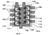
- FIG. 7 shows a schematic plan view of the internal configuration of a conventional power semiconductor device disclosed in Patent Document 1, for example.
- a gate electrode 111 is provided on the surface of each element, and a source electrode 121s is provided in a region other than the gate electrode 111 on the surface of each element.
- a drain electrode is provided on the back surface of each element.
- the first present invention provides: A first metal wiring connected to the first external connection terminal; A second metal wiring connected to the second external connection terminal; A third metal wiring connected to the third external connection terminal; A first power semiconductor element group including three or more first power semiconductor elements mounted on the first metal wiring; A second power semiconductor element group including the same number of second power semiconductor elements as the first power semiconductor elements mounted on the second metal wiring; The electrode of the first power semiconductor element is connected to the second metal wiring by the first conductive member, and the electrode of the second power semiconductor element is connected to the third metal wiring and the first metal wiring.
- the resistance value of the region where the first power semiconductor element group or the second power semiconductor element group is mounted is in the direction in which the current flows.
- the downstream side is larger than the upstream side, or the region where the first conductive member or the second conductive member is connected among the second metal wiring and the third metal wiring.
- the power semiconductor device is characterized in that the resistance value is smaller on the downstream side than on the upstream side with respect to the current flow direction.
- the second aspect of the present invention Of the first, second and third metal wirings, a region where the first and second power semiconductor element groups are mounted and a region where the first and second conductive members are connected Is a substantially linear shape, and the linear regions of the first, second and third metal wirings are arranged substantially parallel to each other.
- the power semiconductor device of the present invention is not limited to the present invention.
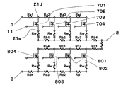
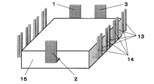
- the power semiconductor device of the present embodiment shown in FIG. 1 includes MOSFETs 7 (701 to 704) as power semiconductor elements that perform switching on the high voltage side and MOSFETs 8 (801 to 801) as power semiconductor elements that perform switching on the low voltage side.
- 804 is a 2-in-1 power module in which four each are mounted in parallel on the lead frame.
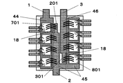
- the region of the metal wiring 4 where the MOSFETs 701 to 704 are mounted is formed so that the wiring width is narrower in the current flow direction, that is, the wiring resistance is increased.
- the region to be connected is formed so as to be thicker in the direction of current flow, that is, to reduce the wiring resistance.
- the variation in the voltage Vds (V) can be reduced as compared with the cases of Examples 1 and 2. That is, the resistance value of the metal wiring in the region where the power semiconductor elements (MOSFETs 701 to 704) are mounted is set to be larger on the downstream side than on the upstream side with respect to the direction of current flow, and the wire is connected. The resistance value of the metal wiring in the region is set so as to be constant in the same manner as in the past in the direction of current flow, and is applied between the source and drain of each power semiconductor element (MOSFETs 701 to 704). It has been found that the voltage can be suppressed from becoming non-uniform.
- the MOSFET is used as the power semiconductor element.
- the present invention is not limited to this, and for example, an IGBT may be used as the power semiconductor element.
- the metal wiring in consideration of a voltage drop due to a large current flowing through the metal wiring, is configured so that the wiring resistance of the metal wiring is increased or decreased with respect to the direction of current flow.
Landscapes
- Engineering & Computer Science (AREA)
- Power Engineering (AREA)
- Inverter Devices (AREA)
- Power Conversion In General (AREA)
Abstract
Description
第一の外部接続端子と接続されている第一の金属配線と、
第二の外部接続端子と接続されている第二の金属配線と、
第三の外部接続端子と接続されている第三の金属配線と、
前記第一の金属配線上に実装された三つ以上の第一のパワー半導体素子を含む第一のパワー半導体素子群と、
前記第二の金属配線上に実装された前記第一のパワー半導体素子と同数の第二のパワー半導体素子を含む第二のパワー半導体素子群とを備え、
前記第一のパワー半導体素子が有する電極が前記第二の金属配線と第一の導電部材により接続されており、且つ、前記第二のパワー半導体素子が有する電極が前記第三の金属配線と第二の導電部材により接続されており、
前記第一の金属配線、及び前記第二の金属配線のうち、前記第一のパワー半導体素子群または前記第二のパワー半導体素子群が実装されている領域の抵抗値は、電流の流れる方向に対して上流側より下流側の方が大きい、または、前記第二の金属配線、及び前記第三の金属配線のうち、前記第一の導電部材または前記第二の導電部材が接続されている領域の抵抗値は、前記電流の流れる方向に対して上流側より下流側の方が小さいことを特徴とする、パワー半導体装置である。
前記第一、第二、及び第三の金属配線のうち、前記第一及び第二のパワー半導体素子群が実装されている領域と、前記第一及び第二の導電部材が接続されている領域は、実質上直線状の形状であり、前記第一、第二、及び第三の金属配線の前記直線状の領域は、互いに実質上平行に配置されていることを特徴とする、上記第1の本発明のパワー半導体装置である。
前記第一のパワー半導体素子群または前記第二のパワー半導体素子群が実装されている前記直線状の領域における幅が、前記電流の流れる方向に対して次第に細くなる、または、
前記第一の導電部材または前記第二の導電部材が接続されている前記直線状の領域における幅が、前記電流の流れる方向に対して次第に太くなることを特徴とする、上記第1または第2の本発明のパワー半導体装置である。
前記第一のパワー半導体素子群または前記第二のパワー半導体素子群が実装されている前記直線状の領域において、スリットまたは切り欠きを設けて前記領域の抵抗値が、前記電流の流れる方向に対して次第に大きくなるように設定されている、または、
前記第一の導電部材または前記第二の導電部材が接続されている前記直線状の領域において、スリットまたは切り欠きを設けて前記領域の抵抗値が、前記電流の流れる方向に対して次第に小さくなるように設定されていることを特徴とする、上記第1または第2の本発明のパワー半導体装置である。
前記第一、第二、及び第三の金属配線の前記直線状の領域のうち、(1)前記第一及び第二の導電部材が接続されている領域の抵抗値は、前記電流の流れる方向に対して次第に小さくなり、且つ、(2)前記第一及び第二のパワー半導体素子群が実装されている領域の抵抗値は、前記電流の流れる方向に対して次第に大きくなることを特徴とする、上記第1または第2の本発明のパワー半導体装置である。
前記第一及び第三の外部接続端子は、前記互いに実質上平行な前記直線状の前記第一及び第三の金属配線の一方の端部と接続されており、前記第二の外部接続端子は、前記一方の端部と反対側において前記第二の金属配線の他方の端部と接続されていることを特徴とする、上記第1乃至第5の何れかの本発明のパワー半導体装置である。
前記パワー半導体装置は、直流電力を交流電力に変換する電力変換装置もしくは電力変換回路を構成する一部分であることを特徴とする、上記第1乃至第6の何れかの本発明のパワー半導体装置である。
前記第一および第三の外部接続端子に直流電圧が印加され、前記第二の外部接続端子から交流電圧が出力されることを特徴とする、上記第7の本発明のパワー半導体装置である。
前記第一または第二のパワー半導体素子は、ソース電極、ドレイン電極、及びゲート電極を備えるMOSFETであり、前記ソース電極および前記ドレイン電極間に寄生ダイオードが形成されていることを特徴とする、上記第1乃至第8の何れかの本発明のパワー半導体装置である。
前記第一または第二のパワー半導体素子群は、三つ以上のスイッチング素子としての前記パワー半導体素子と一つ以上の整流素子を含むことを特徴とする、上記第1乃至第8の何れかの本発明のパワー半導体装置である。
図1は、本発明の一実施の形態にかかるパワー半導体装置の内部構成を示す概略平面図である。






図4、5、6は、本発明の他の実施の形態にかかるパワー半導体装置の内部構成を示す概略平面図である。
2,102 外部接続端子(第二の外部接続端子)
3,103 外部接続端子(第三の外部接続端子)
4,24,34,44,104 金属配線(第一の金属配線)
5,25,35,45,105 金属配線(第二の金属配線)
6,26,36,46,106 金属配線(第三の金属配線)
107、701~704 MOSFET(第一のパワー半導体素子)
108、801~804 MOSFET(第二のパワー半導体素子)
9,109 ワイヤ(第一の導電部材)
10,110 ワイヤ(第二の導電部材)
11,111 ゲート電極
12,112 ボンディングワイヤ
13,113 ゲート電極端子
14,114 ソース電極端子
15,115 モールド樹脂
16 配線抵抗調整用のスリットパターン
17 配線抵抗調整用の切り欠きパターン
18 配線抵抗調整用の凹凸パターン
Claims (10)
- 第一の外部接続端子と接続されている第一の金属配線と、
第二の外部接続端子と接続されている第二の金属配線と、
第三の外部接続端子と接続されている第三の金属配線と、
前記第一の金属配線上に実装された三つ以上の第一のパワー半導体素子を含む第一のパワー半導体素子群と、
前記第二の金属配線上に実装された前記第一のパワー半導体素子と同数の第二のパワー半導体素子を含む第二のパワー半導体素子群とを備え、
前記第一のパワー半導体素子が有する電極が前記第二の金属配線と第一の導電部材により接続されており、且つ、前記第二のパワー半導体素子が有する電極が前記第三の金属配線と第二の導電部材により接続されており、
前記第一の金属配線、及び前記第二の金属配線のうち、前記第一のパワー半導体素子群または前記第二のパワー半導体素子群が実装されている領域の抵抗値は、電流の流れる方向に対して上流側より下流側の方が大きい、または、前記第二の金属配線、及び前記第三の金属配線のうち、前記第一の導電部材または前記第二の導電部材が接続されている領域の抵抗値は、前記電流の流れる方向に対して上流側より下流側の方が小さいことを特徴とする、パワー半導体装置。 - 前記第一、第二、及び第三の金属配線のうち、前記第一及び第二のパワー半導体素子群が実装されている領域と、前記第一及び第二の導電部材が接続されている領域は、実質上直線状の形状であり、前記第一、第二、及び第三の金属配線の前記直線状の領域は、互いに実質上平行に配置されていることを特徴とする、請求項1に記載のパワー半導体装置。
- 前記第一のパワー半導体素子群または前記第二のパワー半導体素子群が実装されている前記直線状の領域における幅が、前記電流の流れる方向に対して次第に細くなる、または、
前記第一の導電部材または前記第二の導電部材が接続されている前記直線状の領域における幅が、前記電流の流れる方向に対して次第に太くなることを特徴とする、請求項1または2に記載のパワー半導体装置。 - 前記第一のパワー半導体素子群または前記第二のパワー半導体素子群が実装されている前記直線状の領域において、スリットまたは切り欠きを設けて前記領域の抵抗値が、前記電流の流れる方向に対して次第に大きくなるように設定されている、または、
前記第一の導電部材または前記第二の導電部材が接続されている前記直線状の領域において、スリットまたは切り欠きを設けて前記領域の抵抗値が、前記電流の流れる方向に対して次第に小さくなるように設定されていることを特徴とする、請求項1または2に記載のパワー半導体装置。 - 前記第一、第二、及び第三の金属配線の前記直線状の領域のうち、(1)前記第一及び第二の導電部材が接続されている領域の抵抗値は、前記電流の流れる方向に対して次第に小さくなり、且つ、(2)前記第一及び第二のパワー半導体素子群が実装されている領域の抵抗値は、前記電流の流れる方向に対して次第に大きくなることを特徴とする、請求項1または2に記載のパワー半導体装置。
- 前記第一及び第三の外部接続端子は、前記互いに実質上平行な前記直線状の前記第一及び第三の金属配線の一方の端部と接続されており、前記第二の外部接続端子は、前記一方の端部と反対側において前記第二の金属配線の他方の端部と接続されていることを特徴とする、請求項1乃至5の何れか一つに記載のパワー半導体装置。
- 前記パワー半導体装置は、直流電力を交流電力に変換する電力変換装置もしくは電力変換回路を構成する一部分であることを特徴とする、請求項1乃至6の何れか一つに記載のパワー半導体装置。
- 前記第一および第三の外部接続端子に直流電圧が印加され、前記第二の外部接続端子から交流電圧が出力されることを特徴とする、請求項7に記載のパワー半導体装置。
- 前記第一または第二のパワー半導体素子は、ソース電極、ドレイン電極、及びゲート電極を備えるMOSFETであり、前記ソース電極および前記ドレイン電極間に寄生ダイオードが形成されていることを特徴とする、請求項1乃至8の何れか一つに記載のパワー半導体装置。
- 前記第一または第二のパワー半導体素子群は、三つ以上のスイッチング素子としての前記パワー半導体素子と一つ以上の整流素子を含むことを特徴とする、請求項1乃至8の何れか一つに記載のパワー半導体装置。
Priority Applications (4)
| Application Number | Priority Date | Filing Date | Title |
|---|---|---|---|
| US14/402,492 US9325257B2 (en) | 2012-06-01 | 2013-04-09 | Power semiconductor device to reduce voltage variation between terminals |
| EP13797797.1A EP2858110B1 (en) | 2012-06-01 | 2013-04-09 | Power semiconductor device |
| JP2014518239A JP5914867B2 (ja) | 2012-06-01 | 2013-04-09 | パワー半導体装置 |
| CN201380028042.XA CN104380462B (zh) | 2012-06-01 | 2013-04-09 | 功率半导体装置 |
Applications Claiming Priority (2)
| Application Number | Priority Date | Filing Date | Title |
|---|---|---|---|
| JP2012-125833 | 2012-06-01 | ||
| JP2012125833 | 2012-06-01 |
Publications (1)
| Publication Number | Publication Date |
|---|---|
| WO2013179547A1 true WO2013179547A1 (ja) | 2013-12-05 |
Family
ID=49672782
Family Applications (1)
| Application Number | Title | Priority Date | Filing Date |
|---|---|---|---|
| PCT/JP2013/002411 Ceased WO2013179547A1 (ja) | 2012-06-01 | 2013-04-09 | パワー半導体装置 |
Country Status (5)
| Country | Link |
|---|---|
| US (1) | US9325257B2 (ja) |
| EP (1) | EP2858110B1 (ja) |
| JP (1) | JP5914867B2 (ja) |
| CN (1) | CN104380462B (ja) |
| WO (1) | WO2013179547A1 (ja) |
Cited By (15)
| Publication number | Priority date | Publication date | Assignee | Title |
|---|---|---|---|---|
| JP2014011225A (ja) * | 2012-06-28 | 2014-01-20 | Sumitomo Electric Ind Ltd | 半導体装置及び半導体装置の製造方法 |
| WO2016050491A1 (de) * | 2014-10-02 | 2016-04-07 | Continental Automotive Gmbh | Leistungsmodul, leistungsmodulgruppe, leistungsendstufe sowie antriebssystem mit einer leistungsendstufe |
| WO2019230292A1 (ja) * | 2018-06-01 | 2019-12-05 | 富士電機株式会社 | 半導体装置 |
| JP2019220563A (ja) * | 2018-06-19 | 2019-12-26 | 新電元工業株式会社 | パワーモジュール及びスイッチング電源 |
| US10964630B2 (en) | 2018-09-21 | 2021-03-30 | Denso Corporation | Semiconductor device having a conductor plate and semiconductor elements |
| CN113224025A (zh) * | 2020-01-21 | 2021-08-06 | 瑞昱半导体股份有限公司 | 半导体组件 |
| JP2021168319A (ja) * | 2020-03-12 | 2021-10-21 | 住友電気工業株式会社 | 半導体装置 |
| JP2022536792A (ja) * | 2019-06-14 | 2022-08-18 | ウルフスピード インコーポレイテッド | パワーエレクトロニクス用のパッケージ |
| JP2022158037A (ja) * | 2021-04-01 | 2022-10-14 | 三菱電機株式会社 | 半導体装置 |
| WO2022249812A1 (ja) * | 2021-05-27 | 2022-12-01 | 株式会社デンソー | 半導体装置 |
| JPWO2022255139A1 (ja) * | 2021-06-04 | 2022-12-08 | ||
| WO2023053823A1 (ja) * | 2021-09-29 | 2023-04-06 | ローム株式会社 | 半導体装置 |
| JPWO2024048077A1 (ja) * | 2022-08-29 | 2024-03-07 | ||
| WO2025248985A1 (ja) * | 2024-05-30 | 2025-12-04 | 富士電機株式会社 | 半導体装置 |
| JP7813329B1 (ja) * | 2024-10-10 | 2026-02-12 | カヤバ株式会社 | 基板 |
Families Citing this family (18)
| Publication number | Priority date | Publication date | Assignee | Title |
|---|---|---|---|---|
| JP2014110555A (ja) * | 2012-12-03 | 2014-06-12 | Samsung Electronics Co Ltd | アンテナ装置 |
| JP6451747B2 (ja) * | 2014-11-28 | 2019-01-16 | 富士電機株式会社 | 半導体装置 |
| JP6594000B2 (ja) | 2015-02-26 | 2019-10-23 | ローム株式会社 | 半導体装置 |
| JP6062565B1 (ja) * | 2015-05-29 | 2017-01-18 | 新電元工業株式会社 | 半導体装置およびその製造方法 |
| JP6582678B2 (ja) * | 2015-07-27 | 2019-10-02 | 三菱電機株式会社 | 半導体装置 |
| CN107431066B (zh) | 2016-03-11 | 2019-08-30 | 新电元工业株式会社 | 半导体装置 |
| CN110050339B (zh) * | 2016-12-16 | 2023-12-22 | 日立能源有限公司 | 具有低栅极通路电感的功率半导体模块 |
| US11107761B2 (en) | 2018-02-06 | 2021-08-31 | Denso Corporation | Semiconductor device |
| JP2019186403A (ja) | 2018-04-11 | 2019-10-24 | トヨタ自動車株式会社 | 半導体装置 |
| EP3654373B1 (en) * | 2018-11-19 | 2021-01-06 | Infineon Technologies AG | Multi-chip-package |
| EP3690939A1 (en) * | 2019-01-30 | 2020-08-05 | Infineon Technologies AG | Semiconductor arrangements |
| JP7198168B2 (ja) * | 2019-07-19 | 2022-12-28 | 株式会社 日立パワーデバイス | パワー半導体モジュール |
| JP7259655B2 (ja) * | 2019-09-04 | 2023-04-18 | 株式会社デンソー | パワーモジュール |
| JP6896831B2 (ja) * | 2019-12-05 | 2021-06-30 | 三菱電機株式会社 | 半導体モジュールおよび電力変換装置 |
| CN113054826A (zh) * | 2019-12-26 | 2021-06-29 | 财团法人工业技术研究院 | 高功率模块 |
| JP7305603B2 (ja) * | 2020-09-18 | 2023-07-10 | 株式会社東芝 | 半導体装置 |
| CN114566477A (zh) * | 2020-11-27 | 2022-05-31 | 苏州东微半导体股份有限公司 | 半导体装置 |
| US11973012B2 (en) | 2021-07-26 | 2024-04-30 | Infineon Technologies Austria Ag | Power module with semiconductor packages mounted on metal frame |
Citations (3)
| Publication number | Priority date | Publication date | Assignee | Title |
|---|---|---|---|---|
| JP2004022960A (ja) | 2002-06-19 | 2004-01-22 | Mitsubishi Electric Corp | 電力用半導体装置 |
| JP2004134460A (ja) * | 2002-10-08 | 2004-04-30 | Mitsubishi Electric Corp | 半導体装置 |
| JP2010034347A (ja) * | 2008-07-30 | 2010-02-12 | Sanyo Electric Co Ltd | 回路装置 |
Family Cites Families (5)
| Publication number | Priority date | Publication date | Assignee | Title |
|---|---|---|---|---|
| DE60132855T2 (de) * | 2000-07-27 | 2009-02-26 | Texas Instruments Inc., Dallas | Kontaktierungsstruktur einer integrierten Leistungsschaltung |
| JP2004273749A (ja) | 2003-03-07 | 2004-09-30 | Fuji Electric Fa Components & Systems Co Ltd | 半導体パワーモジュール |
| JP2004296998A (ja) * | 2003-03-28 | 2004-10-21 | Matsushita Electric Ind Co Ltd | 半導体装置 |
| JP2009158830A (ja) * | 2007-12-27 | 2009-07-16 | Sanyo Electric Co Ltd | 素子搭載用基板およびその製造方法、半導体モジュールおよびその製造方法、ならびに携帯機器 |
| JPWO2012039115A1 (ja) * | 2010-09-24 | 2014-02-03 | セミコンダクター・コンポーネンツ・インダストリーズ・リミテッド・ライアビリティ・カンパニー | 回路装置 |
-
2013
- 2013-04-09 CN CN201380028042.XA patent/CN104380462B/zh not_active Expired - Fee Related
- 2013-04-09 US US14/402,492 patent/US9325257B2/en not_active Expired - Fee Related
- 2013-04-09 JP JP2014518239A patent/JP5914867B2/ja not_active Expired - Fee Related
- 2013-04-09 WO PCT/JP2013/002411 patent/WO2013179547A1/ja not_active Ceased
- 2013-04-09 EP EP13797797.1A patent/EP2858110B1/en active Active
Patent Citations (3)
| Publication number | Priority date | Publication date | Assignee | Title |
|---|---|---|---|---|
| JP2004022960A (ja) | 2002-06-19 | 2004-01-22 | Mitsubishi Electric Corp | 電力用半導体装置 |
| JP2004134460A (ja) * | 2002-10-08 | 2004-04-30 | Mitsubishi Electric Corp | 半導体装置 |
| JP2010034347A (ja) * | 2008-07-30 | 2010-02-12 | Sanyo Electric Co Ltd | 回路装置 |
Non-Patent Citations (1)
| Title |
|---|
| See also references of EP2858110A4 |
Cited By (35)
| Publication number | Priority date | Publication date | Assignee | Title |
|---|---|---|---|---|
| JP2014011225A (ja) * | 2012-06-28 | 2014-01-20 | Sumitomo Electric Ind Ltd | 半導体装置及び半導体装置の製造方法 |
| WO2016050491A1 (de) * | 2014-10-02 | 2016-04-07 | Continental Automotive Gmbh | Leistungsmodul, leistungsmodulgruppe, leistungsendstufe sowie antriebssystem mit einer leistungsendstufe |
| US10236806B2 (en) | 2014-10-02 | 2019-03-19 | Continental Automotive Gmbh | Power module, power module group, power output stage, and drive system comprising a power output stage |
| US11373988B2 (en) | 2018-06-01 | 2022-06-28 | Fuji Electric Co., Ltd. | Semiconductor device |
| WO2019230292A1 (ja) * | 2018-06-01 | 2019-12-05 | 富士電機株式会社 | 半導体装置 |
| JPWO2019230292A1 (ja) * | 2018-06-01 | 2020-12-17 | 富士電機株式会社 | 半導体装置 |
| JP7060094B2 (ja) | 2018-06-01 | 2022-04-26 | 富士電機株式会社 | 半導体装置 |
| JP7237475B2 (ja) | 2018-06-19 | 2023-03-13 | 新電元工業株式会社 | パワーモジュール及びスイッチング電源 |
| JP2019220563A (ja) * | 2018-06-19 | 2019-12-26 | 新電元工業株式会社 | パワーモジュール及びスイッチング電源 |
| US10964630B2 (en) | 2018-09-21 | 2021-03-30 | Denso Corporation | Semiconductor device having a conductor plate and semiconductor elements |
| US12400986B2 (en) | 2019-06-14 | 2025-08-26 | Wolfspeed, Inc. | Package for power electronics |
| JP2022536792A (ja) * | 2019-06-14 | 2022-08-18 | ウルフスピード インコーポレイテッド | パワーエレクトロニクス用のパッケージ |
| JP2023134790A (ja) * | 2019-06-14 | 2023-09-27 | ウルフスピード インコーポレイテッド | パワーエレクトロニクス用のパッケージ |
| JP7320083B2 (ja) | 2019-06-14 | 2023-08-02 | ウルフスピード インコーポレイテッド | パワーエレクトロニクス用のパッケージ |
| JP7652840B2 (ja) | 2019-06-14 | 2025-03-27 | ウルフスピード インコーポレイテッド | パワーエレクトロニクス用のパッケージ |
| US11756910B2 (en) | 2019-06-14 | 2023-09-12 | Wolfspeed, Inc. | Package for power electronics |
| US11887953B2 (en) | 2019-06-14 | 2024-01-30 | Wolfspeed, Inc. | Package for power electronics |
| CN113224025A (zh) * | 2020-01-21 | 2021-08-06 | 瑞昱半导体股份有限公司 | 半导体组件 |
| JP2021168319A (ja) * | 2020-03-12 | 2021-10-21 | 住友電気工業株式会社 | 半導体装置 |
| US11942411B2 (en) | 2021-04-01 | 2024-03-26 | Mitsubishi Electric Corporation | Semiconductor device |
| JP7531444B2 (ja) | 2021-04-01 | 2024-08-09 | 三菱電機株式会社 | 半導体装置 |
| JP2022158037A (ja) * | 2021-04-01 | 2022-10-14 | 三菱電機株式会社 | 半導体装置 |
| JP2022181821A (ja) * | 2021-05-27 | 2022-12-08 | 株式会社デンソー | 半導体装置 |
| JP7563296B2 (ja) | 2021-05-27 | 2024-10-08 | 株式会社デンソー | 半導体装置 |
| WO2022249812A1 (ja) * | 2021-05-27 | 2022-12-01 | 株式会社デンソー | 半導体装置 |
| WO2022255139A1 (ja) * | 2021-06-04 | 2022-12-08 | 富士電機株式会社 | 半導体装置 |
| JP7622835B2 (ja) | 2021-06-04 | 2025-01-28 | 富士電機株式会社 | 半導体装置 |
| JPWO2022255139A1 (ja) * | 2021-06-04 | 2022-12-08 | ||
| WO2023053823A1 (ja) * | 2021-09-29 | 2023-04-06 | ローム株式会社 | 半導体装置 |
| JPWO2024048077A1 (ja) * | 2022-08-29 | 2024-03-07 | ||
| WO2024048077A1 (ja) * | 2022-08-29 | 2024-03-07 | 富士電機株式会社 | 半導体装置 |
| JP7740566B2 (ja) | 2022-08-29 | 2025-09-17 | 富士電機株式会社 | 半導体装置 |
| WO2025248985A1 (ja) * | 2024-05-30 | 2025-12-04 | 富士電機株式会社 | 半導体装置 |
| JP7813329B1 (ja) * | 2024-10-10 | 2026-02-12 | カヤバ株式会社 | 基板 |
| WO2026079066A1 (ja) * | 2024-10-10 | 2026-04-16 | カヤバ株式会社 | 基板 |
Also Published As
| Publication number | Publication date |
|---|---|
| EP2858110B1 (en) | 2020-04-08 |
| JPWO2013179547A1 (ja) | 2016-01-18 |
| CN104380462A (zh) | 2015-02-25 |
| EP2858110A4 (en) | 2015-07-29 |
| CN104380462B (zh) | 2017-05-24 |
| US20150155797A1 (en) | 2015-06-04 |
| US9325257B2 (en) | 2016-04-26 |
| EP2858110A1 (en) | 2015-04-08 |
| JP5914867B2 (ja) | 2016-05-11 |
Similar Documents
| Publication | Publication Date | Title |
|---|---|---|
| JP5914867B2 (ja) | パワー半導体装置 | |
| CN106026692B (zh) | 半导体模块、电力变换装置以及半导体模块的制造方法 | |
| CN207233730U (zh) | 电子装置 | |
| US9754863B2 (en) | Semiconductor device | |
| EP2760121B1 (en) | Electronic circuit | |
| CN108336055B (zh) | 用于均匀分布的电流流动的引线框架上的交指器件 | |
| CN103325759B (zh) | 半导体模块 | |
| JP5056595B2 (ja) | 電力変換装置 | |
| JPWO2016056320A1 (ja) | 半導体装置及びバスバー | |
| JPWO2019229894A1 (ja) | 半導体モジュールおよび電力変換装置 | |
| JP3896940B2 (ja) | 半導体装置 | |
| JP2015099843A (ja) | 半導体装置 | |
| US10855196B2 (en) | Semiconductor device | |
| US20230078823A1 (en) | Semiconductor device | |
| US10148190B2 (en) | Power conversion device | |
| CN111769723A (zh) | 具有附加发射极/源极路径的并联功率模块 | |
| US9337174B2 (en) | Semiconductor device for suppressing inductance | |
| CN106411107B (zh) | 电力转换装置 | |
| CN222300677U (zh) | 功率模块和电子器件 | |
| US20240333168A1 (en) | Multi-level power module with reduced parasitic effects | |
| TW202450058A (zh) | 半導體裝置及使用其之電力轉換裝置 | |
| CN103824838A (zh) | 集成电路组件 | |
| CN118738041A (zh) | 具有减少的寄生效应的多级功率模块 | |
| CN118355493A (zh) | 半导体模块 | |
| CN120418963A (zh) | 功率半导体装置 |
Legal Events
| Date | Code | Title | Description |
|---|---|---|---|
| 121 | Ep: the epo has been informed by wipo that ep was designated in this application |
Ref document number: 13797797 Country of ref document: EP Kind code of ref document: A1 |
|
| ENP | Entry into the national phase |
Ref document number: 2014518239 Country of ref document: JP Kind code of ref document: A |
|
| WWE | Wipo information: entry into national phase |
Ref document number: 14402492 Country of ref document: US |
|
| WWE | Wipo information: entry into national phase |
Ref document number: 2013797797 Country of ref document: EP |
|
| NENP | Non-entry into the national phase |
Ref country code: DE |