WO2013179820A1 - 半導体装置 - Google Patents
半導体装置 Download PDFInfo
- Publication number
- WO2013179820A1 WO2013179820A1 PCT/JP2013/061898 JP2013061898W WO2013179820A1 WO 2013179820 A1 WO2013179820 A1 WO 2013179820A1 JP 2013061898 W JP2013061898 W JP 2013061898W WO 2013179820 A1 WO2013179820 A1 WO 2013179820A1
- Authority
- WO
- WIPO (PCT)
- Prior art keywords
- layer
- conductivity type
- type pillar
- semiconductor device
- trench
- Prior art date
- Legal status (The legal status is an assumption and is not a legal conclusion. Google has not performed a legal analysis and makes no representation as to the accuracy of the status listed.)
- Ceased
Links
Images

Classifications
-
- H—ELECTRICITY
- H10—SEMICONDUCTOR DEVICES; ELECTRIC SOLID-STATE DEVICES NOT OTHERWISE PROVIDED FOR
- H10D—INORGANIC ELECTRIC SEMICONDUCTOR DEVICES
- H10D62/00—Semiconductor bodies, or regions thereof, of devices having potential barriers
- H10D62/80—Semiconductor bodies, or regions thereof, of devices having potential barriers characterised by the materials
- H10D62/83—Semiconductor bodies, or regions thereof, of devices having potential barriers characterised by the materials being Group IV materials, e.g. B-doped Si or undoped Ge
- H10D62/832—Semiconductor bodies, or regions thereof, of devices having potential barriers characterised by the materials being Group IV materials, e.g. B-doped Si or undoped Ge being Group IV materials comprising two or more elements, e.g. SiGe
- H10D62/8325—Silicon carbide
-
- B—PERFORMING OPERATIONS; TRANSPORTING
- B08—CLEANING
- B08B—CLEANING IN GENERAL; PREVENTION OF FOULING IN GENERAL
- B08B9/00—Cleaning hollow articles by methods or apparatus specially adapted thereto
- B08B9/02—Cleaning pipes or tubes or systems of pipes or tubes
- B08B9/027—Cleaning the internal surfaces; Removal of blockages
- B08B9/032—Cleaning the internal surfaces; Removal of blockages by the mechanical action of a moving fluid, e.g. by flushing
- B08B9/0321—Cleaning the internal surfaces; Removal of blockages by the mechanical action of a moving fluid, e.g. by flushing using pressurised, pulsating or purging fluid
-
- B—PERFORMING OPERATIONS; TRANSPORTING
- B08—CLEANING
- B08B—CLEANING IN GENERAL; PREVENTION OF FOULING IN GENERAL
- B08B9/00—Cleaning hollow articles by methods or apparatus specially adapted thereto
- B08B9/02—Cleaning pipes or tubes or systems of pipes or tubes
- B08B9/027—Cleaning the internal surfaces; Removal of blockages
- B08B9/032—Cleaning the internal surfaces; Removal of blockages by the mechanical action of a moving fluid, e.g. by flushing
- B08B9/0321—Cleaning the internal surfaces; Removal of blockages by the mechanical action of a moving fluid, e.g. by flushing using pressurised, pulsating or purging fluid
- B08B9/0328—Cleaning the internal surfaces; Removal of blockages by the mechanical action of a moving fluid, e.g. by flushing using pressurised, pulsating or purging fluid by purging the pipe with a gas or a mixture of gas and liquid
-
- H—ELECTRICITY
- H10—SEMICONDUCTOR DEVICES; ELECTRIC SOLID-STATE DEVICES NOT OTHERWISE PROVIDED FOR
- H10D—INORGANIC ELECTRIC SEMICONDUCTOR DEVICES
- H10D30/00—Field-effect transistors [FET]
- H10D30/60—Insulated-gate field-effect transistors [IGFET]
- H10D30/64—Double-diffused metal-oxide semiconductor [DMOS] FETs
- H10D30/66—Vertical DMOS [VDMOS] FETs
- H10D30/668—Vertical DMOS [VDMOS] FETs having trench gate electrodes, e.g. UMOS transistors
-
- H—ELECTRICITY
- H10—SEMICONDUCTOR DEVICES; ELECTRIC SOLID-STATE DEVICES NOT OTHERWISE PROVIDED FOR
- H10D—INORGANIC ELECTRIC SEMICONDUCTOR DEVICES
- H10D62/00—Semiconductor bodies, or regions thereof, of devices having potential barriers
- H10D62/10—Shapes, relative sizes or dispositions of the regions of the semiconductor bodies; Shapes of the semiconductor bodies
- H10D62/102—Constructional design considerations for preventing surface leakage or controlling electric field concentration
- H10D62/103—Constructional design considerations for preventing surface leakage or controlling electric field concentration for increasing or controlling the breakdown voltage of reverse-biased devices
- H10D62/105—Constructional design considerations for preventing surface leakage or controlling electric field concentration for increasing or controlling the breakdown voltage of reverse-biased devices by having particular doping profiles, shapes or arrangements of PN junctions; by having supplementary regions, e.g. junction termination extension [JTE]
- H10D62/109—Reduced surface field [RESURF] PN junction structures
- H10D62/111—Multiple RESURF structures, e.g. double RESURF or 3D-RESURF structures
-
- H—ELECTRICITY
- H10—SEMICONDUCTOR DEVICES; ELECTRIC SOLID-STATE DEVICES NOT OTHERWISE PROVIDED FOR
- H10D—INORGANIC ELECTRIC SEMICONDUCTOR DEVICES
- H10D62/00—Semiconductor bodies, or regions thereof, of devices having potential barriers
- H10D62/10—Shapes, relative sizes or dispositions of the regions of the semiconductor bodies; Shapes of the semiconductor bodies
- H10D62/17—Semiconductor regions connected to electrodes not carrying current to be rectified, amplified or switched, e.g. channel regions
- H10D62/393—Body regions of DMOS transistors or IGBTs
Definitions
- the present invention relates to a silicon carbide semiconductor device having a low on-resistance and a high breakdown voltage using a silicon carbide substrate.
- a trench gate type MOSFET As a semiconductor switching device for power conversion using a silicon carbide substrate, a trench gate type MOSFET has a small unit cell structure and a high current density, and is therefore effective in reducing on-resistance.
- the super junction structure in which p-type and n-type pillars are repeatedly formed in the drift layer is effective in reducing the drift layer resistance.
- FIG. 2 of Patent Document 1 discloses a structure having a p-type pillar layer between trench gates. Yes.
- the electric field exists not only in the vertical direction from the p base to the drain but also in the horizontal direction from the pillar, and the electric field does not concentrate on a specific portion. Therefore, a high breakdown voltage can be maintained even if the n-type impurity concentration of the n-type pillar layer, which is an on-state current path, is increased.
- silicon carbide has a dielectric breakdown electric field about an order of magnitude higher than that of silicon, silicon carbide can maintain a high electric field.
- a high electric field is also applied to the insulating oxide film present in the periphery, and the conventional structure. Then, the high electric field is applied to the gate oxide film at the bottom of the trench, and there is a possibility that the element is destroyed due to the dielectric breakdown of the insulating oxide film at a low voltage before the silicon carbide reaches the dielectric breakdown.
- Patent Document 2 discloses a structure in which the p base is deepened at a position away from the trench. As a result, a depletion layer extends from the p base, and the trench gate oxide film is protected from a high electric field in the blocking state, element breakdown due to dielectric breakdown of the oxide film is suppressed, and high breakdown voltage is obtained.
- Patent Document 3 discloses a structure in which a high-concentration p-type region is provided at a junction portion between a super junction structure and a p-base.
- the present invention provides a structure for protecting a gate oxide film from a high electric field in a super junction structure of a trench gate type MOSFET using silicon carbide as a substrate material.
- the second conductivity type pillar layer is divided into an upper layer in contact with the base layer and a lower layer therebelow, and the impurity concentration of the upper layer is The impurity concentration of the lower layer is higher than that of the lower layer, and the interface between the upper layer and the lower layer of the second conductivity type pillar layer and the contact between the interface and the first conductivity type pillar layer are located below the bottom of the trench groove.
- the n-type pillar layer adjacent to the upper part of the p-type pillar is depleted at a lower voltage than the lower part in the blocking state.
- the contact point between the upper layer of the p-type pillar layer and the n-type pillar exists below the trench gate oxide film, the gate oxide film is surrounded by the depletion layer and can be shielded from a high electric field. Element breakdown due to dielectric breakdown of the film is suppressed, and a high breakdown voltage is obtained.
- the present invention also provides the above-described semiconductor device, wherein the width of the second conductivity type pillar is such that the upper layer portion is the same as or wider than the lower layer portion.
- the above-described semiconductor device is provided in which the second conductivity type pillar layer has a stripe shape parallel to the trench groove as viewed from above.
- the semiconductor device according to the above, wherein the second conductivity type pillar layer has a stripe shape perpendicular to the trench groove when viewed from above.
- the above-described semiconductor device is provided in which the second conductivity type pillar layers are dotted in an island shape when viewed from above, and the trench grooves are hexagonal shapes centering on the pillar layers.
- the n-type pillar layer adjacent to the upper layer portion of the p-type pillar in the blocking state is lower than the lower layer. Since the contact point between the upper layer of the p-type pillar layer and the n-type pillar exists below the trench gate oxide film, the gate oxide film is surrounded by the depletion layer, and a high electric field is generated. Therefore, element breakdown due to dielectric breakdown of the oxide film is suppressed, and high breakdown voltage can be obtained.
- FIG. 1 shows a cross-sectional view of a unit structure (unit cell) of a stripe-shaped or island-shaped semiconductor device according to the present invention.
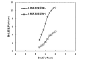
- FIG. 2 is a diagram showing the cell pitch dependence of the oxide film electric field characteristics when the impurity concentration of the p-type pillar is uniform and when the concentration is increased in the upper layer.
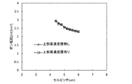
- FIG. 3 is a diagram showing the cell pitch dependence of the on-resistance characteristics when the impurity concentration of the p-type pillar is uniform and when the impurity concentration is increased in the upper layer.
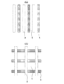
- FIG. 4A is a schematic plan view of a stripe-shaped semiconductor device in which a p-type pillar and a gate trench according to the present invention are arranged in parallel.
- FIG. 4B is a schematic plan view of a stripe-shaped semiconductor device in which the p-type pillar and the gate trench of the present invention are arranged vertically.
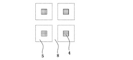
- FIG. 5 is a schematic plan view of a semiconductor device in which an n-type pillar surrounds an island-shaped p-type pillar of the present invention.
- FIG. 1 is a sectional view of a unit structure (unit cell) of a stripe-shaped or island-shaped semiconductor device according to the first embodiment.
- a drift layer 2 is deposited on a 4H—SiC low resistance n + type substrate 1.
- a p-type pillar 4 and an n-type pillar 5 constituting the super junction region 3 are periodically and repeatedly disposed thereon.
- the shape seen from above is a structure in which an n-type pillar surrounds a stripe or island-shaped p-type pillar, for example, a hexagon. Since the upper part of the p-type pillar layer is a high-concentration p-type layer 6 and the concentration ratio with the n-type pillar is high, the upper part of the n-type pillar is depleted at a lower voltage than the lower part in the blocking state.
- a p-type base layer 7 is laminated on the super junction region 3, and a gate trench 8 reaching the super junction region 3 from the surface is formed.
- the direction in which the gate trench 8 is viewed from above is arbitrary, such as parallel to the pillars (FIG. 4 (a)) or perpendicular (FIG. 4 (b)) when the pillar arrangement is a stripe as shown in FIG. I can do it.
- the gate trench is disposed so as to penetrate inside the n-type pillar layer. Further, as shown in FIG. 5, even when the p-type pillar is island-shaped, the gate trench is formed along the shape of the n-type pillar surrounding the p-type pillar so as to penetrate the inside of the n-type pillar.
- a gate insulating film 9 and a gate electrode 10 are formed inside the gate trench 8.
- a high concentration n + source region 11 is selectively formed on the surface of the p-type base layer 7 so as to be adjacent to the gate trench 8, and a high concentration p + base contact region 12 is selectively formed between the source regions 11. Yes.
- the source electrode 13 is connected to a part of the source region 11 and the base contact region 12 with a low resistance, and is led upward through the interlayer insulating film 14.
- a drain electrode 15 is connected to the back surface of the substrate with a low resistance.
- FIG. 2 and FIG. 3 show the result of comparing the cell pitch dependence of the oxide film characteristics and the on-resistance characteristics when the impurity concentration of the p-type pillar is uniform and when the impurity concentration is increased in the upper layer.
- the cell pitch is changed according to the width of the n-type pillar.
- the electric field applied to the gate oxide film in the blocking state of FIG. 2 is greatly reduced by increasing the concentration of the upper portion of the p-type pillar, while the on-resistance of FIG. 3 is not different between the two structures. It can be seen that the electric field suppression to the oxide film is achieved without sacrificing other characteristics by increasing the concentration of the upper part of the p-type pillar.
Landscapes
- Engineering & Computer Science (AREA)
- Mechanical Engineering (AREA)
- Electrodes Of Semiconductors (AREA)
Description
また、ドリフト層の抵抗が支配的となる高耐圧装置において、ドリフト層内にp型とn型のピラーを繰り返し形成したスーパージャンクション構造は、ドリフト層抵抗の低減に効果的である。これらの構造を組み合わせることにより、低抵抗で高耐圧のスイッチング装置が実現できる。
よってオン状態の電流経路であるn型ピラー層のn型不純物濃度を高くしても高耐圧を維持できる。
これによりpベースから空乏層が延びトレンチゲート酸化膜が阻止状態において高電界から保護され、酸化膜の絶縁破壊による素子破壊が抑制され、高い耐圧が得られる。
よってトレンチゲートのスーパージャンクション構造に適した酸化膜を保護する構造が必要となる。
特許文献3は、スーパージャンクション構造とpベースの接合部分に高濃度のp型領域を設けた構造を開示している。
これによりブレークダウンを高濃度のp型領域の底面で発生できるので、アバランシェ電流をp+コンタクトに流しやすくなり、アバランシェ耐量を向上させることが出来る。
しかしながら、トレンチゲート酸化膜を保護する効果に関して明らかでない。
これにより、阻止状態においてp型ピラー上層部に隣接するn型ピラー層がより低電圧で空乏化することができ、酸化膜の絶縁破壊による素子破壊が抑制され、高い耐圧が得られる。
4H-SiCの低抵抗n+型基板1上にドリフト層2が堆積されている。
その上にスーパージャンクション領域3を構成するp型ピラー4とn型ピラー5が周期的に繰り返し配置されている。
p型ピラー層の上部は高濃度p型層6となっており、n型ピラーとの濃度比が高くなるため、阻止状態においてn型ピラーの上部が下部よりも低電圧で空乏化される。
また、図5に示したようにp型ピラーが島状の場合もゲートトレンチの形状はn型ピラーの内側に貫通するよう、p型ピラーを取り囲むn型ピラーの形状に沿って形成される。
基板裏面にはドレイン電極15が低抵抗接続されている。
セルピッチはn型ピラーの幅によって変化させている。
2 ドリフト層
3 スーパージャンクション領域
4 p型ピラー
5 n型ピラー
6 高濃度p型層
7 p型ベース層
8 ゲートトレンチ
9 ゲート絶縁膜(酸化膜)
10 ゲート電極
11 高濃度n+ソース領域
12 高濃度p+ベースコンタクト領域
13 ソース電極
14 層間絶縁膜
15 ドレイン電極
Claims (5)
- 炭化珪素基板上の第1の導電型のドリフト層と、
その上に積層した第2の導電型のベース層と、
ベース層の表面部の所定領域に形成された第1導電型のソース領域と、
ソース領域とベース領域を貫通するように形成したトレンチ溝と、
トレンチ溝内の少なくとも一部にゲート絶縁膜を介して形成したゲート電極と、
ドリフト層内にベース層と接するように形成した第2導電型のピラー層からなるスーパージャンクション層を備え、
前記第2導電型のピラー層はベース層に接する上部層とその下の下部層に分かれており、
上部層の不純物濃度が下部層の不純物濃度よりも高く、
前記第2導電型のピラー層の上部層と下部層の界面および前記界面と第1の導電型ピラー層との接点がトレンチ溝の底部よりも下方に位置する、
ことを特徴とする半導体装置。 - 前記第2導電型のピラーの幅は上層部が下層部と同じもしくは広いことを特徴とする請求項1に記載の半導体装置。
- 前記第2導電型のピラー層は上方から見てトレンチ溝と平行なストライプ形状である請求項1乃至請求項2のいずれか1項に記載の半導体装置。
- 前記第2導電型のピラー層は上方から見てトレンチ溝と垂直なストライプ形状である請求項1乃至請求項2のいずれか1項に記載の半導体装置。
- 前記第2導電型のピラー層は上方から見て島状に点在しトレンチ溝はピラー層を中心とした六角形状である請求項1乃至請求項2のいずれか1項に記載の半導体装置。
Priority Applications (3)
| Application Number | Priority Date | Filing Date | Title |
|---|---|---|---|
| EP13797744.3A EP2860761A4 (en) | 2012-05-31 | 2013-04-23 | SEMICONDUCTOR COMPONENT |
| US14/404,490 US20150171169A1 (en) | 2012-05-31 | 2013-04-23 | Semiconductor device |
| JP2014518346A JPWO2013179820A1 (ja) | 2012-05-31 | 2013-04-23 | 半導体装置 |
Applications Claiming Priority (2)
| Application Number | Priority Date | Filing Date | Title |
|---|---|---|---|
| JP2012125173 | 2012-05-31 | ||
| JP2012-125173 | 2012-05-31 |
Publications (1)
| Publication Number | Publication Date |
|---|---|
| WO2013179820A1 true WO2013179820A1 (ja) | 2013-12-05 |
Family
ID=49668760
Family Applications (1)
| Application Number | Title | Priority Date | Filing Date |
|---|---|---|---|
| PCT/JP2013/061898 Ceased WO2013179820A1 (ja) | 2012-05-31 | 2013-04-23 | 半導体装置 |
Country Status (4)
| Country | Link |
|---|---|
| US (1) | US20150171169A1 (ja) |
| EP (1) | EP2860761A4 (ja) |
| JP (1) | JPWO2013179820A1 (ja) |
| WO (1) | WO2013179820A1 (ja) |
Cited By (4)
| Publication number | Priority date | Publication date | Assignee | Title |
|---|---|---|---|---|
| WO2020129175A1 (ja) * | 2018-12-19 | 2020-06-25 | サンケン電気株式会社 | 半導体装置 |
| JP2024024279A (ja) * | 2022-08-09 | 2024-02-22 | 三菱電機株式会社 | 炭化珪素半導体装置の製造方法 |
| US12170312B2 (en) | 2021-03-08 | 2024-12-17 | Fuji Electric Co., Ltd. | Super junction silicon carbide semiconductor device and manufacturing method thereof |
| US12520549B2 (en) | 2022-03-24 | 2026-01-06 | Kabushiki Kaisha Toshiba | Silicon carbide semiconductor device including alternately provided pillars having different impurity concentrations |
Families Citing this family (2)
| Publication number | Priority date | Publication date | Assignee | Title |
|---|---|---|---|---|
| CN105576022B (zh) * | 2014-10-11 | 2019-02-22 | 华润微电子(重庆)有限公司 | 具有超结结构的半导体器件及其制备方法 |
| CN110116120B (zh) * | 2019-04-23 | 2024-01-09 | 佛山市妇幼保健院 | 一种橡胶吸球的清洗消毒装置 |
Citations (4)
| Publication number | Priority date | Publication date | Assignee | Title |
|---|---|---|---|---|
| JP2009043966A (ja) | 2007-08-09 | 2009-02-26 | Toshiba Corp | 半導体装置及びその製造方法 |
| JP2009260253A (ja) | 2008-03-26 | 2009-11-05 | Rohm Co Ltd | 半導体装置およびその製造方法 |
| JP2012039082A (ja) | 2010-07-12 | 2012-02-23 | Denso Corp | 半導体装置およびその製造方法 |
| JP2012164707A (ja) * | 2011-02-03 | 2012-08-30 | Panasonic Corp | 半導体装置およびその製造方法 |
Family Cites Families (10)
| Publication number | Priority date | Publication date | Assignee | Title |
|---|---|---|---|---|
| JPH10229190A (ja) * | 1997-02-14 | 1998-08-25 | Denso Corp | 炭化珪素半導体装置及びその製造方法 |
| JP3913564B2 (ja) * | 2002-01-31 | 2007-05-09 | 富士電機ホールディングス株式会社 | 超接合半導体素子の製造方法 |
| JP4536366B2 (ja) * | 2003-12-22 | 2010-09-01 | 株式会社豊田中央研究所 | 半導体装置とその設計支援用プログラム |
| JP4813762B2 (ja) * | 2003-12-25 | 2011-11-09 | ルネサスエレクトロニクス株式会社 | 半導体装置及びその製造方法 |
| JP5132123B2 (ja) * | 2006-11-01 | 2013-01-30 | 株式会社東芝 | 電力用半導体素子 |
| JP2008300420A (ja) * | 2007-05-29 | 2008-12-11 | Nec Electronics Corp | 半導体装置及び半導体装置の製造方法 |
| US20090057713A1 (en) * | 2007-08-31 | 2009-03-05 | Infineon Technologies Austria Ag | Semiconductor device with a semiconductor body |
| JP2009302436A (ja) * | 2008-06-17 | 2009-12-24 | Denso Corp | 炭化珪素半導体装置の製造方法 |
| JP2011044513A (ja) * | 2009-08-20 | 2011-03-03 | National Institute Of Advanced Industrial Science & Technology | 炭化珪素半導体装置 |
| JP5740108B2 (ja) * | 2010-07-16 | 2015-06-24 | 株式会社東芝 | 半導体装置 |
-
2013
- 2013-04-23 EP EP13797744.3A patent/EP2860761A4/en not_active Withdrawn
- 2013-04-23 US US14/404,490 patent/US20150171169A1/en not_active Abandoned
- 2013-04-23 JP JP2014518346A patent/JPWO2013179820A1/ja active Pending
- 2013-04-23 WO PCT/JP2013/061898 patent/WO2013179820A1/ja not_active Ceased
Patent Citations (4)
| Publication number | Priority date | Publication date | Assignee | Title |
|---|---|---|---|---|
| JP2009043966A (ja) | 2007-08-09 | 2009-02-26 | Toshiba Corp | 半導体装置及びその製造方法 |
| JP2009260253A (ja) | 2008-03-26 | 2009-11-05 | Rohm Co Ltd | 半導体装置およびその製造方法 |
| JP2012039082A (ja) | 2010-07-12 | 2012-02-23 | Denso Corp | 半導体装置およびその製造方法 |
| JP2012164707A (ja) * | 2011-02-03 | 2012-08-30 | Panasonic Corp | 半導体装置およびその製造方法 |
Non-Patent Citations (1)
| Title |
|---|
| See also references of EP2860761A4 |
Cited By (5)
| Publication number | Priority date | Publication date | Assignee | Title |
|---|---|---|---|---|
| WO2020129175A1 (ja) * | 2018-12-19 | 2020-06-25 | サンケン電気株式会社 | 半導体装置 |
| US12170312B2 (en) | 2021-03-08 | 2024-12-17 | Fuji Electric Co., Ltd. | Super junction silicon carbide semiconductor device and manufacturing method thereof |
| US12520549B2 (en) | 2022-03-24 | 2026-01-06 | Kabushiki Kaisha Toshiba | Silicon carbide semiconductor device including alternately provided pillars having different impurity concentrations |
| JP2024024279A (ja) * | 2022-08-09 | 2024-02-22 | 三菱電機株式会社 | 炭化珪素半導体装置の製造方法 |
| JP7702923B2 (ja) | 2022-08-09 | 2025-07-04 | 三菱電機株式会社 | 炭化珪素半導体装置の製造方法 |
Also Published As
| Publication number | Publication date |
|---|---|
| EP2860761A1 (en) | 2015-04-15 |
| US20150171169A1 (en) | 2015-06-18 |
| EP2860761A4 (en) | 2016-02-24 |
| JPWO2013179820A1 (ja) | 2016-01-18 |
Similar Documents
| Publication | Publication Date | Title |
|---|---|---|
| US8957502B2 (en) | Semiconductor device | |
| JP5580150B2 (ja) | 半導体装置 | |
| JP5852555B2 (ja) | 半導体装置 | |
| JP4967236B2 (ja) | 半導体素子 | |
| US10276654B2 (en) | Semiconductor device with parallel PN structures | |
| JP6805620B2 (ja) | 半導体装置 | |
| JP5701913B2 (ja) | 半導体装置 | |
| JP5297706B2 (ja) | 半導体装置 | |
| JP6720818B2 (ja) | 半導体装置 | |
| JP2016009712A (ja) | 炭化珪素半導体装置 | |
| WO2013179820A1 (ja) | 半導体装置 | |
| US8829563B2 (en) | Power semiconductor device and method for manufacturing such a power semiconductor device | |
| JP2014038963A (ja) | 半導体装置 | |
| JP5694285B2 (ja) | 半導体装置 | |
| US9048313B2 (en) | Semiconductor device that can maintain high voltage while lowering on-state resistance | |
| JP6169985B2 (ja) | 半導体装置 | |
| JP6299658B2 (ja) | 絶縁ゲート型スイッチング素子 | |
| US20150053998A1 (en) | Semiconductor device | |
| JP7326991B2 (ja) | スイッチング素子 | |
| US9356100B2 (en) | Semiconductor device | |
| JP7147510B2 (ja) | スイッチング素子 | |
| JP5719407B2 (ja) | 半導体装置 | |
| JP5798517B2 (ja) | 半導体装置 | |
| JP6458994B2 (ja) | 半導体装置 | |
| US9502498B2 (en) | Power semiconductor device |
Legal Events
| Date | Code | Title | Description |
|---|---|---|---|
| 121 | Ep: the epo has been informed by wipo that ep was designated in this application |
Ref document number: 13797744 Country of ref document: EP Kind code of ref document: A1 |
|
| ENP | Entry into the national phase |
Ref document number: 2014518346 Country of ref document: JP Kind code of ref document: A |
|
| NENP | Non-entry into the national phase |
Ref country code: DE |
|
| REEP | Request for entry into the european phase |
Ref document number: 2013797744 Country of ref document: EP |
|
| WWE | Wipo information: entry into national phase |
Ref document number: 2013797744 Country of ref document: EP |
|
| WWE | Wipo information: entry into national phase |
Ref document number: 14404490 Country of ref document: US |