WO2014002501A1 - Connecteur électrique - Google Patents
Connecteur électrique Download PDFInfo
- Publication number
- WO2014002501A1 WO2014002501A1 PCT/JP2013/004015 JP2013004015W WO2014002501A1 WO 2014002501 A1 WO2014002501 A1 WO 2014002501A1 JP 2013004015 W JP2013004015 W JP 2013004015W WO 2014002501 A1 WO2014002501 A1 WO 2014002501A1
- Authority
- WO
- WIPO (PCT)
- Prior art keywords
- terminal
- housing
- female terminal
- electrical connector
- insertion hole
- Prior art date
- Legal status (The legal status is an assumption and is not a legal conclusion. Google has not performed a legal analysis and makes no representation as to the accuracy of the status listed.)
- Ceased
Links
Images


Classifications
-
- H—ELECTRICITY
- H01—ELECTRIC ELEMENTS
- H01R—ELECTRICALLY-CONDUCTIVE CONNECTIONS; STRUCTURAL ASSOCIATIONS OF A PLURALITY OF MUTUALLY-INSULATED ELECTRICAL CONNECTING ELEMENTS; COUPLING DEVICES; CURRENT COLLECTORS
- H01R12/00—Structural associations of a plurality of mutually-insulated electrical connecting elements, specially adapted for printed circuits, e.g. printed circuit boards [PCB], flat or ribbon cables, or like generally planar structures, e.g. terminal strips, terminal blocks; Coupling devices specially adapted for printed circuits, flat or ribbon cables, or like generally planar structures; Terminals specially adapted for contact with, or insertion into, printed circuits, flat or ribbon cables, or like generally planar structures
- H01R12/70—Coupling devices
- H01R12/71—Coupling devices for rigid printing circuits or like structures
- H01R12/712—Coupling devices for rigid printing circuits or like structures co-operating with the surface of the printed circuit or with a coupling device exclusively provided on the surface of the printed circuit
- H01R12/716—Coupling device provided on the PCB
-
- H—ELECTRICITY
- H01—ELECTRIC ELEMENTS
- H01R—ELECTRICALLY-CONDUCTIVE CONNECTIONS; STRUCTURAL ASSOCIATIONS OF A PLURALITY OF MUTUALLY-INSULATED ELECTRICAL CONNECTING ELEMENTS; COUPLING DEVICES; CURRENT COLLECTORS
- H01R13/00—Details of coupling devices of the kinds covered by groups H01R12/70 or H01R24/00 - H01R33/00
- H01R13/62—Means for facilitating engagement or disengagement of coupling parts or for holding them in engagement
- H01R13/629—Additional means for facilitating engagement or disengagement of coupling parts, e.g. aligning or guiding means, levers, gas pressure electrical locking indicators, manufacturing tolerances
-
- H—ELECTRICITY
- H01—ELECTRIC ELEMENTS
- H01R—ELECTRICALLY-CONDUCTIVE CONNECTIONS; STRUCTURAL ASSOCIATIONS OF A PLURALITY OF MUTUALLY-INSULATED ELECTRICAL CONNECTING ELEMENTS; COUPLING DEVICES; CURRENT COLLECTORS
- H01R13/00—Details of coupling devices of the kinds covered by groups H01R12/70 or H01R24/00 - H01R33/00
- H01R13/64—Means for preventing incorrect coupling
- H01R13/642—Means for preventing incorrect coupling by position or shape of contact members
-
- H—ELECTRICITY
- H01—ELECTRIC ELEMENTS
- H01R—ELECTRICALLY-CONDUCTIVE CONNECTIONS; STRUCTURAL ASSOCIATIONS OF A PLURALITY OF MUTUALLY-INSULATED ELECTRICAL CONNECTING ELEMENTS; COUPLING DEVICES; CURRENT COLLECTORS
- H01R13/00—Details of coupling devices of the kinds covered by groups H01R12/70 or H01R24/00 - H01R33/00
- H01R13/62—Means for facilitating engagement or disengagement of coupling parts or for holding them in engagement
- H01R13/629—Additional means for facilitating engagement or disengagement of coupling parts, e.g. aligning or guiding means, levers, gas pressure electrical locking indicators, manufacturing tolerances
- H01R13/631—Additional means for facilitating engagement or disengagement of coupling parts, e.g. aligning or guiding means, levers, gas pressure electrical locking indicators, manufacturing tolerances for engagement only
Definitions
- the present invention relates to an electrical connector having a housing in which a lead of a counterpart terminal is formed.
- a male connector that holds a male terminal and a female connector that holds a female terminal that is electrically connected to the male terminal are usually fitted to each other.
- a guide is provided in the housing of the female connector through which the male terminal is inserted (for example, Patent Document 1 FIG. 8).
- the lead-in is a taper shape in which the surface on the side where the male terminal is inserted is tapered around the insertion hole of the housing through which the male terminal penetrates.
- the male terminal can be guided to the insertion hole of the housing even if there is a slight displacement.
- the male terminal may be fitted to the female terminal while being displaced.
- the displacement of the male terminal can be reduced, but there is a limit when considering that the housing is manufactured by injection molding of resin.
- the length of the insertion hole in the direction in which the male terminal is inserted in other words, the thickness of the housing wall provided with the insertion hole is increased, the displacement of the male terminal can be reduced.
- an object of the present invention is to provide an electrical connector capable of reducing the displacement of a male terminal as a counterpart terminal without increasing the size of a housing.
- the electrical connector of the present invention is a housing having a terminal X electrically connected to the counterpart terminal Y, and an insertion hole for holding the terminal X and inserting the counterpart terminal Y when electrical connection is made. And comprising.
- This housing has a guide formed on the surface on the side where the mating terminal Y is inserted, around the insertion hole, and a regulation protrusion formed on the back surface opposite to the surface and corresponding to the guide. , Provided.
- the restricting projection is formed in the housing in response to the lug, and therefore, even if the thickness of the housing is increased, it remains in a limited region, so that the size of the housing is not substantially increased. .
- the restricting protrusion the displacement of the male terminal can be reduced.
- the distance from the apex of the restriction projection to the contact point between the terminal X and the counterpart terminal Y is L1, and from the back surface around the restriction projection, When the distance to the contact is L2, it is preferable to satisfy L1 ⁇ L2.
- the housing may include a first housing disposed outside and a second housing disposed inside the first housing.
- the guiding and restricting protrusions are formed in the first housing, and the concave portion for accommodating the restricting protrusions is formed in the second housing.
- the displacement of the male terminal can be reduced without increasing the size of the housing.
- FIG. 3 is a partially enlarged view of FIG. 2.
- the electrical connector 1 includes a female terminal 10 and a housing 5 that houses the female terminal 10.
- the female terminal 10 is electrically connected to the first male terminal 3 and the second male terminal 4, and the housing 5 is fixed to the circuit board 6.
- the first male terminal 3 is fixed to the circuit board 6, and the second male terminal 4 is fixed to another device arranged below the circuit board 6 in the figure.
- the electrical connector 1 achieves the object of the present invention by being characterized by the shape around the lead-in 37 formed in the first housing 30 constituting the housing 5.
- each component of the electrical connector 1 will be described in order.
- the female terminal 10 includes a first female terminal 11, a second female terminal 12, and a connecting spring 20 that connects the first female terminal 11 and the second female terminal 12.
- the female terminal 10 is formed by integrally cutting the first female terminal 11, the second female terminal 12, and the connecting spring 20 by cutting and bending a highly conductive metal plate such as copper or copper alloy. Is formed.
- the first female terminal 11 and the second female terminal 12 which are manufactured to have substantially the same shape and dimensions (specifications) are connected by the connecting spring 20 by shifting the position of the first male terminals 3 and 4 in the insertion / extraction direction A. It is.
- the first female terminal 11 accommodates a box-shaped terminal body 13 in which a receiving port 14 into which the first male terminal 3 is inserted is opened on one end side, and the first male terminal 3 inserted from the receiving port 14.
- a connecting spring 20 is integrally connected to the other end side of the terminal body 13.
- the main leaf 16 overlaps the first male terminal 3 because it is drawn at a no-load position where the first male terminal 3 is not inserted.
- a locking protrusion 18 is formed on the outer wall of the terminal body 13.
- the locking protrusion 18 is used to position the female terminal 10 with respect to the housing 5 and prevent the female terminal 10 from coming off by being locked to the housing 5 in a state where the female terminal 10 is mounted on the housing 5. Since the second female terminal 12 has substantially the same specifications as the first female terminal 11, the same components as those of the first female terminal 11 are denoted by the same reference numerals, and the description thereof is omitted. However, when the female terminal 10 is mounted on the housing 5, the second female terminal 12 is disposed at a position closer to the circuit board 6 than the first female terminal 11. Further, the locking projection 18 of the second female terminal 12 functions when the first male terminal 3 and the second female terminal 12 are fitted, as will be described later.
- the connection spring 20 that connects the first female terminal 11 and the second female terminal 12 includes a pair of columnar portions 21 and 22 and a beam portion 23 that connects the tips of the columnar portions 21 and 22. Since the columnar portions 21 and 22 are formed along the insertion / extraction direction A, the columnar portions 21 and 22 mainly bend in the width direction B (FIG. 1) orthogonal to the insertion / extraction direction A. The beam portion 23 can be easily bent mainly in the insertion / extraction direction A by forming an S-shape to reduce the spring constant.
- first male terminal 3, second male terminal 4 The tab-shaped first male terminal 3 and second male terminal 4 are fitted with the first female terminal 11 and the second female terminal 12, respectively, as shown in FIG.
- the L-shaped first male terminal 3 is fixed to the first surface 7 of the circuit board 6. Fixing is performed by soldering (not shown), for example. Further, the straight second male terminal 4 is fixed to an electric device (not shown).
- the first male terminal 3 is electrically connected to the first female terminal 11 by inserting the distal end of the first male terminal 3 into the receiving cavity 15 of the first female terminal 11.
- the first male terminal 3 that receives the pressing force from the elastically deforming main leaf 16 and sub-leaf 17 is pressed against the inner wall of the terminal body 13, thereby electrically connecting the first female terminal 11 and the first male terminal 3. Is maintained.
- the second male terminal 4 that receives a pressing force from the elastically deformed main leaf 16 and sub-leaf 17 is pressed against the inner wall of the terminal body 13, so that the second female terminal 12 and the second male terminal 4 Electrical connection is maintained.
- An insertion hole 8 penetrating the front and back is formed in the circuit board 6, and the second male terminal 4 is inserted into the receiving cavity 15 therethrough.
- the housing 5 is fixed on the circuit board 6 and accommodates the female terminal 10 therein.
- the housing 5 in the present embodiment includes three elements: a first housing 30, a second housing 40, and a third housing 50.
- the housing 5 is mounted in the order of the first housing 30, the second housing 40 and the third housing 50 from the circuit board 6 side. Note that these housing elements are manufactured by injection molding an insulating resin.
- the first housing 30 has a shape in which a cap is generally turned upside down, and a terminal holding floor 31 facing the circuit board 6, and a terminal holding floor A side wall 35 rising from the peripheral edge of 31, and a housing recess 36 surrounded by the terminal holding floor 31 and the side wall 35 are provided.
- the terminal holding floor 31 is formed with an insertion hole 32 through which the first male terminal 3 is inserted and an insertion hole 33 through which the second male terminal 4 is inserted.
- the opening size of the insertion hole 32 is set so that the first male terminal 3 is press-fitted.
- the opening size of the insertion hole 33 is set so as to have play (clearance) between the second male terminal 4 to be inserted.
- the insertion through the hole with play is referred to as loose fitting.
- the terminal holding floor 31 is formed so that the portion where the insertion hole 32 is formed is thicker than the portion where the insertion hole 33 is formed so that the first male terminal 3 is held by the terminal holding floor 31 with sufficient force. ing.
- the difference in thickness corresponds to the amount of positional deviation between the first female terminal 11 and the second female terminal 12.
- a guide 37 is formed in which the periphery of the insertion hole 33 is tapered.
- the surface of the terminal holding floor 31 that faces the circuit board 6 is the front surface, and the opposite surface is the back surface.
- a regulation protrusion 38 is formed around the insertion hole 33 corresponding to the guide 37. As shown in FIG. 1, the restricting protrusion 38 has a trapezoidal appearance.
- the restricting protrusion 38 is inserted into the guide 49 (FIG. 3) of the second housing 40.
- the regulation protrusion 38 is provided in a thin portion of the terminal holding floor 31.
- the terminal holding floor 31 provided with the insertion hole 32 is formed thick, but the insertion hole 33 is formed in relation to the second female terminal 12 being arranged at a position close to the circuit board 6.
- the thickness of the terminal holding floor 31 is reduced at the portion where the terminal is provided.
- This background is also related to the provision of the restricting projections 38 instead of increasing the thickness of the terminal holding floor 31.
- a peg 34 for fixing the first housing 30 to the first surface 7 of the circuit board 6 is provided on the surface of the terminal holding floor 31.
- the first housing 30 is fixed to the circuit board 6 by soldering the pegs 34 to the first surface 7.
- the housing recess 36 In the housing recess 36, the first male terminal 3 and the second male terminal 4 penetrating the terminal holding floor 31 and the female terminal 10 fitted thereto are accommodated.
- the housing recess 36 accommodates a second housing 40 and a third housing 50 that hold the female terminal 10, and these housings are fixed to the first housing 30.
- the second housing 40 includes a bottom floor 41 that faces the terminal holding floor 31 of the first housing 30, a side wall 45 that rises from the periphery of the bottom floor 41, and a bottom floor 41 and a side wall 45. And a partition 46 that divides the region surrounded by two into the receiving recesses 47 and 48.
- the bottom floor 41 is formed with an insertion hole 42 through which the first male terminal 3 is inserted and an insertion hole 43 through which the second male terminal 4 is inserted.
- the first male terminal 3 is loosely fitted in the insertion hole 42, and the second male terminal 4 is loosely fitted in the insertion hole 43.
- a guide 49 that is recessed in a taper shape around the insertion hole 43 is formed.
- the restriction protrusion 38 of the first housing 30 is inserted into the guide 49. Therefore, the invitation 49 has a space that can sufficiently accommodate the restricting protrusion 38.
- the first female terminal 11 is housed in the housing recess 47 and the second female terminal 12 is housed in the housing recess 48.
- the first female terminal 11 is held by the second housing 40 as one end (lower end) where the receiving port 14 is formed contacts the bottom floor 41 and the locking projection 18 is locked to the upper end of the side wall 45.
- the second female terminal 12 has one end (lower end) where the receiving port 14 is formed away from the bottom floor 41, and a play is provided between the side wall 45 and the partition 46 around the second female terminal 12.
- a gap is provided between the locking projection 18 of the second female terminal 12 and the upper end of the side wall 45 in contact with the housing recess 48. Therefore, the second female terminal 12 is suspended in the interior of the housing recess 48 via the connecting spring 20.
- the third housing 50 has a generally cap shape and includes a female terminal 10, a first male terminal 3, and a second male terminal 4.
- the first housing 30 is mounted so as to cover the upper portions of the first housing 30 and the second housing 40. Although illustration is omitted, the third housing 50 is detached from the first housing 30 by engaging the lock piece formed on the first housing 30 and the lock piece formed on the third housing 50. It has been stopped.
- the third housing 50 includes a ceiling 51, side walls 52 (52 ⁇ / b> A, 52 ⁇ / b> B) that hang down from the periphery of the ceiling 51, and an accommodation recess 53 that is surrounded by the ceiling 51 and the side walls 52.
- the lower end of the side wall 52 ⁇ / b> A contacts the locking protrusion 18 of the first female terminal 11. Accordingly, the first female terminal 11 is fixed to the housing 5 by the locking projection 18 being sandwiched from above and below by the side wall 45 of the second housing 40 and the side wall 52A of the third housing 50. Since the first housing 30 is fixed to the first surface 7 of the circuit board 6, the housing 5 is equivalent to the first female terminal 11 being fixed to the circuit board 6.
- a gap is provided between the lower end of the side wall 52B and the locking projection 18 of the second female terminal 12 with the third housing 50 mounted. Therefore, in this state, the locking projection 18 of the second female terminal 12 is not mechanically restrained.
- the coupling spring 20 is accommodated in the accommodating recess 53, but the ceiling 51 and the side wall 52 are provided along the coupling spring 20 with a small space therebetween.
- a pressing protrusion 54 that protrudes in the horizontal direction is formed on the ceiling 51 that intersects the side wall 52B. The pressing protrusion 54 is used when fitting the second male terminal 4 and the second female terminal 12 together.
- the electrical connector 1 can reduce the displacement of the second male terminal 4 by providing the terminal protrusion 31 with the restricting protrusion 38 on the terminal holding floor 31 of the first housing 30.
- the reason is as follows.
- the second male terminal 4 is loosely fitted in the insertion hole 33.
- Have difficulty If this inclination increases, the positional deviation at the desired contact between the second male terminal 4 and the second female terminal 12 increases, so it is necessary to reduce this inclination.
- the contact CP is normally determined at the design stage of the electrical connector 1.
- the first element is the length of the insertion hole 33 in the insertion / extraction direction
- the second element is the distance to the contact point between the second male terminal 4 and the second female terminal 12.
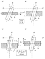
- FIG. 6 schematically showing the periphery of the insertion hole 33.
- 6A shows the case where the length of the insertion hole 33 in the insertion / extraction direction, in other words, the thickness of the terminal holding floor 31 around the insertion hole 33 is thin (t1)
- FIG. 6B shows the terminal holding floor 31. This shows a case where the thickness of (2) is large (t2).
- the second male terminal 4 to be inserted is shown as being inclined to the maximum inside the insertion hole 33.
- the contact between the second male terminal 4 and the second female terminal 12 is CP
- the positional deviation from the axial direction of the second male terminal 4 at the contact CP is apparent from FIGS. 6 (a) and 6 (b).
- the thickness of the terminal holding floor 31 is smaller in FIG. 6B (first element).
- the distance to the contact CP is different, as is clear from FIGS. 6C and 6D, the distance to the contact CP is shorter.
- the positional deviation from the axial direction of the second male terminal 4 at the contact CP is small (second element).
- providing the restricting protrusion 38 in addition to the invitation 37 means that the two elements are simultaneously provided. That is, compared with the case where the surface of the terminal holding floor 31 is kept flat without providing the restricting protrusion 38, the portion where the restricting protrusion 38 is provided is thicker in the terminal holding floor 31. With elements.
- a second element is provided since the distance from the end on the back side of the insertion hole 33 to the contact position is shortened by providing the restricting protrusion 38, a second element is provided.
- the electrical connector 1 can reduce the displacement of the second male terminal 4.
- the electrical connector 1 is formed with the restricting projection 38 only around the insertion hole 33, and the restricting projection 38 is inserted into the guide 49 of the second housing 40. Therefore, if the second housing 40 is also taken into consideration. The thickness of the housing 5 around the insertion hole 33 is not increased.
- the first female terminal 11 and the second female terminal 12 are arranged with their positions shifted in the insertion / extraction direction. By doing so, the timing at which the male terminal 3 is fitted to the first female terminal 11 and the timing at which the second male terminal 4 is fitted to the second female terminal 12 are shifted. Therefore, compared with the 1st female terminal 11 and the 2nd female terminal 12 being arrange
- the distance from the contact point between the main leaf 16 and the first male terminal 4 to the other end side of the second female terminal 12 is set as necessary. Since it can be made long, it is easy to ensure an effective contact length between the second male terminal 4 and the second female terminal 12.
- the electrical connector 1 has a trapezoidal appearance of the restricting projection 38, which is derived from the fact that the second male terminal 4 has a tab (flat) shape. Therefore, the appearance of the restriction protrusion can be specified according to the shape of the male terminal. For example, if the cross section of the male terminal is circular, the restriction protrusion forms a truncated cone.
- the electrical connector 1 includes a second housing 40 in which a guide 49 for accommodating the restriction protrusion 38 is formed, and further a third housing 50.
- the present invention can be applied to an electrical connector including only a housing corresponding to the first housing 30.
- the housing for accommodating the restricting protrusion 38 is not provided, but the restricting protrusion 38 exists only in a very limited range, so that it is hardly an obstacle to the assembly of the electrical connector with other members. .
- the configuration described in the above embodiment can be selected or changed to another configuration as appropriate.
Landscapes
- Coupling Device And Connection With Printed Circuit (AREA)
- Connector Housings Or Holding Contact Members (AREA)
Applications Claiming Priority (2)
| Application Number | Priority Date | Filing Date | Title |
|---|---|---|---|
| JP2012145263A JP2014010951A (ja) | 2012-06-28 | 2012-06-28 | 電気コネクタ |
| JP2012-145263 | 2012-06-28 |
Publications (1)
| Publication Number | Publication Date |
|---|---|
| WO2014002501A1 true WO2014002501A1 (fr) | 2014-01-03 |
Family
ID=49782688
Family Applications (1)
| Application Number | Title | Priority Date | Filing Date |
|---|---|---|---|
| PCT/JP2013/004015 Ceased WO2014002501A1 (fr) | 2012-06-28 | 2013-06-27 | Connecteur électrique |
Country Status (2)
| Country | Link |
|---|---|
| JP (1) | JP2014010951A (fr) |
| WO (1) | WO2014002501A1 (fr) |
Citations (4)
| Publication number | Priority date | Publication date | Assignee | Title |
|---|---|---|---|---|
| JPH0227682U (fr) * | 1988-08-10 | 1990-02-22 | ||
| JP2006216308A (ja) * | 2005-02-02 | 2006-08-17 | Sumitomo Wiring Syst Ltd | コネクタ |
| JP2007005239A (ja) * | 2005-06-27 | 2007-01-11 | Sumitomo Wiring Syst Ltd | コネクタ |
| JP2011044291A (ja) * | 2009-08-20 | 2011-03-03 | Sumitomo Wiring Syst Ltd | コネクタ |
Family Cites Families (3)
| Publication number | Priority date | Publication date | Assignee | Title |
|---|---|---|---|---|
| JP3462096B2 (ja) * | 1998-11-05 | 2003-11-05 | 住友電装株式会社 | 基板用コネクタ |
| JP4175774B2 (ja) * | 2000-12-12 | 2008-11-05 | 矢崎総業株式会社 | コネクタ |
| JP3836755B2 (ja) * | 2002-06-19 | 2006-10-25 | 住友電装株式会社 | 電気接続箱 |
-
2012
- 2012-06-28 JP JP2012145263A patent/JP2014010951A/ja active Pending
-
2013
- 2013-06-27 WO PCT/JP2013/004015 patent/WO2014002501A1/fr not_active Ceased
Patent Citations (4)
| Publication number | Priority date | Publication date | Assignee | Title |
|---|---|---|---|---|
| JPH0227682U (fr) * | 1988-08-10 | 1990-02-22 | ||
| JP2006216308A (ja) * | 2005-02-02 | 2006-08-17 | Sumitomo Wiring Syst Ltd | コネクタ |
| JP2007005239A (ja) * | 2005-06-27 | 2007-01-11 | Sumitomo Wiring Syst Ltd | コネクタ |
| JP2011044291A (ja) * | 2009-08-20 | 2011-03-03 | Sumitomo Wiring Syst Ltd | コネクタ |
Also Published As
| Publication number | Publication date |
|---|---|
| JP2014010951A (ja) | 2014-01-20 |
Similar Documents
| Publication | Publication Date | Title |
|---|---|---|
| JP5964673B2 (ja) | 電気コネクタ及びメス型端子 | |
| JP6385815B2 (ja) | コネクタ組立体 | |
| JP6525221B2 (ja) | コネクタ | |
| JP5602617B2 (ja) | コネクタ部材 | |
| JP5955448B2 (ja) | コネクタ | |
| EP2903093A1 (fr) | Connecteur électrique | |
| JP5947972B2 (ja) | 電子部品の組付構造及び電子部品 | |
| JP2015060628A (ja) | コネクタ | |
| WO2012095934A1 (fr) | Structure de verrouillage de borne dans un logement de connecteur | |
| JP5959719B2 (ja) | 電子部品の組付構造及び電気接続箱 | |
| CN107809037A (zh) | 电连接器以及电连接器组装体 | |
| CN110534951A (zh) | 连接器 | |
| JP2018181404A (ja) | 電気コネクタ | |
| JP2016054095A (ja) | コネクタ | |
| JP2018006246A (ja) | 端子モジュール、およびコネクタ | |
| JP2015099683A (ja) | コネクタ | |
| CN113675638A (zh) | 电路基板用电连接器 | |
| CN105281080A (zh) | 连接器端子和包括该连接器端子的连接器 | |
| JP2012243563A (ja) | コネクタ端子及びこのコネクタ端子を含むカードエッジ型コネクタ | |
| JPWO2014142250A1 (ja) | 電子部品の組付構造及び電気接続箱 | |
| JP2019053841A (ja) | コネクタ | |
| CN112018535A (zh) | 电连接器组装体 | |
| WO2014002501A1 (fr) | Connecteur électrique | |
| JP6746357B2 (ja) | コネクタ端子およびコネクタ | |
| JP5986912B2 (ja) | 端子 |
Legal Events
| Date | Code | Title | Description |
|---|---|---|---|
| 121 | Ep: the epo has been informed by wipo that ep was designated in this application |
Ref document number: 13809065 Country of ref document: EP Kind code of ref document: A1 |
|
| NENP | Non-entry into the national phase |
Ref country code: DE |
|
| 122 | Ep: pct application non-entry in european phase |
Ref document number: 13809065 Country of ref document: EP Kind code of ref document: A1 |