WO2014017109A1 - 集積型光モジュール - Google Patents
集積型光モジュール Download PDFInfo
- Publication number
- WO2014017109A1 WO2014017109A1 PCT/JP2013/004569 JP2013004569W WO2014017109A1 WO 2014017109 A1 WO2014017109 A1 WO 2014017109A1 JP 2013004569 W JP2013004569 W JP 2013004569W WO 2014017109 A1 WO2014017109 A1 WO 2014017109A1
- Authority
- WO
- WIPO (PCT)
- Prior art keywords
- adhesive
- plc chip
- optical module
- optical
- groove
- Prior art date
- Legal status (The legal status is an assumption and is not a legal conclusion. Google has not performed a legal analysis and makes no representation as to the accuracy of the status listed.)
- Ceased
Links
Images




Classifications
-
- G—PHYSICS
- G02—OPTICS
- G02B—OPTICAL ELEMENTS, SYSTEMS OR APPARATUS
- G02B6/00—Light guides; Structural details of arrangements comprising light guides and other optical elements, e.g. couplings
- G02B6/10—Light guides; Structural details of arrangements comprising light guides and other optical elements, e.g. couplings of the optical waveguide type
- G02B6/12—Light guides; Structural details of arrangements comprising light guides and other optical elements, e.g. couplings of the optical waveguide type of the integrated circuit kind
- G02B6/122—Basic optical elements, e.g. light-guiding paths
-
- G—PHYSICS
- G02—OPTICS
- G02B—OPTICAL ELEMENTS, SYSTEMS OR APPARATUS
- G02B6/00—Light guides; Structural details of arrangements comprising light guides and other optical elements, e.g. couplings
- G02B6/24—Coupling light guides
- G02B6/42—Coupling light guides with opto-electronic elements
- G02B6/4201—Packages, e.g. shape, construction, internal or external details
- G02B6/4219—Mechanical fixtures for holding or positioning the elements relative to each other in the couplings; Alignment methods for the elements, e.g. measuring or observing methods especially used therefor
- G02B6/4236—Fixing or mounting methods of the aligned elements
- G02B6/4239—Adhesive bonding; Encapsulation with polymer material
-
- G—PHYSICS
- G02—OPTICS
- G02B—OPTICAL ELEMENTS, SYSTEMS OR APPARATUS
- G02B6/00—Light guides; Structural details of arrangements comprising light guides and other optical elements, e.g. couplings
- G02B6/24—Coupling light guides
- G02B6/26—Optical coupling means
- G02B6/30—Optical coupling means for use between fibre and thin-film device
-
- G—PHYSICS
- G02—OPTICS
- G02B—OPTICAL ELEMENTS, SYSTEMS OR APPARATUS
- G02B6/00—Light guides; Structural details of arrangements comprising light guides and other optical elements, e.g. couplings
- G02B6/24—Coupling light guides
- G02B6/42—Coupling light guides with opto-electronic elements
- G02B6/4201—Packages, e.g. shape, construction, internal or external details
- G02B6/4219—Mechanical fixtures for holding or positioning the elements relative to each other in the couplings; Alignment methods for the elements, e.g. measuring or observing methods especially used therefor
- G02B6/4236—Fixing or mounting methods of the aligned elements
- G02B6/4244—Mounting of the optical elements
Definitions
- the present invention relates to an integrated optical module, and more particularly to an integrated optical module equipped with a planar lightwave circuit integrated with a light emitting element or a light receiving element to constitute an optical transceiver.
- a general transceiver configuration includes a light emitting element or a light receiving element manufactured using an optical semiconductor and an output or input optical fiber, which are optically coupled via a lens.
- a light emitting element or a light receiving element manufactured using an optical semiconductor
- an output or input optical fiber which are optically coupled via a lens.
- light emitted from an optical fiber on the input side is imaged on a light receiving element by a lens and directly detected (intensity detection).
- phase shift keying (PSK) method is a method of transmitting a signal by modulating the phase of light.
- PSK system can dramatically increase the transmission capacity compared to the prior art by increasing the number of modulations.
- the light receiving element can detect the intensity of the signal light, but cannot directly detect the phase of the light. Therefore, a means for converting the phase of light into light intensity is required. Therefore, there is a method of detecting a phase difference by using light interference.
- signal light and other light reference light
- a light receiving element By causing signal light and other light (reference light) to interfere with each other and detecting the light intensity of the interference light with a light receiving element, it is possible to obtain phase information of the light.
- coherent detection using a light source prepared separately as reference light and differential detection in which part of the signal light itself is branched to interfere with both as reference light.
- a recent PSK optical receiver requires an optical interference circuit that converts phase information into intensity information by light interference. ing.
- Such an optical interference circuit can be realized by using a planar lightwave circuit (PLC: Planar Light Circuit).
- PLC Planar Lightwave circuit
- the PLC has excellent features in terms of mass productivity, low cost, and high reliability, and various optical interference circuits can be realized.
- an optical interference circuit used for a PSK optical receiver an optical delay interference circuit, a 90-degree hybrid circuit, and the like have been realized and put into practical use.
- PLCs are manufactured by standard photolithography, etching techniques, and glass deposition techniques such as FHD (Flame Hydrolysis Deposition).
- an under cladding layer made mainly of quartz glass or the like and a core layer having a higher refractive index than that of the under cladding layer are deposited on a substrate such as Si.
- a substrate such as Si.
- waveguides with various patterns are formed in the core layer.
- the waveguide is embedded with an overcladding layer.
- FIG. 1 shows an optical connection method between a conventional PLC and an optical receiver.
- the basic connection method between the PLC and the optical receiver in the PSK optical receiver is a simple fiber connection as shown in FIG.
- Optical coupling is performed by connecting a planar lightwave circuit (PLC) 1 having an optical fiber 3a connected to the input end and an optical receiver 2 with an optical fiber 3b.
- PLC planar lightwave circuit
- the number of optical fibers 3b used for optical coupling is determined by the number of output lights output from the PLC. There may be a case where the number of optical fibers used for optical coupling is plural. Therefore, there is a problem that the size of the optical receiver using such an optical fiber connection is increased.
- the optical receiver can be miniaturized by optically coupling the output of the PLC and the input of the optical receiver directly without going through an optical fiber and integrating the whole in one package.
- Such an optical receiver in which the PLC and the optical receiver are directly optically coupled is referred to as an integrated optical module.
- a method for fixing a PLC chip is particularly important.
- the light output from the PLC chip is propagated into the space and optically coupled to the light receiving element by a lens or the like, all light is received if the positional relationship among the light emitting end from the PLC chip, the lens, and the light receiving element changes. Light cannot be received by the element, resulting in loss.
- the environmental temperature changes and the temperature of the package that houses the optical receiver, the temperature of each element, etc. change these positions fluctuate due to the effects of thermal expansion. Become.
- it is necessary that the positional relationship does not change at least relatively even when the environmental temperature or the like changes.
- the area occupied by the PLC chip in the optical receiver is about one to two digits larger than that of the light receiving element, and the shape change due to thermal expansion is large.
- the substrate constituting the planar lightwave circuit and the deposited thin film glass have a large difference in thermal expansion coefficient, a large warp occurs due to a temperature change.
- the positional displacement and emission angle change of the emitted light from the PLC chip with respect to the light receiving element are very problematic.
- These two changes change the position and angle of the emitted light from the planar lightwave circuit, causing an optical axis shift.
- the optical axis shift deteriorates the optical coupling to the light receiving element and generates a loss. In order to realize an integrated optical module, it is important to eliminate such an optical axis shift or make it harmless.
- Fig. 2 shows the internal structure of a conventional integrated optical module.
- the PLC chip 13 in which an optical interference circuit is formed as an optical functional circuit, the lens 14, and the light receiving element 15 are each provided with mounting mounts 12 a, 12 b, and 12 c as support members.
- the base substrate 11 is fixed.
- the optical fiber 16 and the PLC chip 13 are connected via an optical fiber fixing component 17.
- the light input from the optical fiber 16 interferes with the PLC chip 13 and is then coupled to the light receiving element 15 by the lens 14.
- the fixing mount 12a and the PLC chip 13 are fixed by an adhesive 18 or solder. By substantially fixing the almost entire bottom surface of the PLC chip 13 to the fixing mount, expansion and warpage change due to temperature are suppressed. Further, the lens 14 and the light receiving element 15 are also fixed to the fixing mount so that the optical axis shift due to temperature change does not occur.
- the optical axis shift due to temperature change can be suppressed to be sufficiently small, but on the other hand, the change in characteristics of the PLC chip due to temperature change becomes significant.
- the planar lightwave circuit 13 is composed of the Si substrate 13a and the quartz glass layer 13b having a large difference in thermal expansion coefficient, warpage change due to temperature change and thermal expansion are large.
- the bottom surface of the PLC chip 13 is fixed all over, thermal expansion and warpage change are suppressed.
- a large thermal stress is generated between the Si substrate 13a and the quartz glass layer 13b.
- the stress causes a refractive index change in the quartz glass layer 13b through the photoelastic effect.
- the length and refractive index of the waveguide are accurately adjusted in order to control the interference characteristics.
- the change in the refractive index generated through the stress causes a change in the equivalent circuit length and changes the characteristics of the interferometer, and thus degrades the characteristics of the optical interference circuit.
- the adhesive 18 is a soft adhesive such as an elastic adhesive, a paste, or a fixing paste in order to suppress the change in optical characteristics by suppressing the generation of thermal stress (for example, , Refer to Patent Document 1), the influence of the optical axis shift described above becomes significant, and loss occurs.
- FIG. 3 an integrated optical module in which optical components such as a PLC chip are integrated.
- the PLC chip 33 is bonded and fixed by applying an adhesive 38 on a pedestal formed by raising a part of the fixing mount 32a.
- Other configurations in FIG. 3 are the same as those in FIG. That is, the optical fiber 36 is connected to the PLC chip 33 using the optical fiber fixing component 37, and the optical components such as the PLC chip 33, the lens 34, and the light receiving element 35 are fixed to the base substrate 31 by the mounting mounts 32 a and 32 b. , 32c.
- this configuration even if distortion or warpage occurs in the PLC chip due to a temperature change, the effect of stress is minimized in the portion of the optical functional circuit, and the characteristic deterioration of the optical functional circuit can be suppressed.
- FIG. 4B is a top view of the mount. As shown in FIG. 4B, since the pedestal 42 having a quadrangular cross section is provided in a part of the mount, the adhesive overflowing on the four sides of the pedestal accumulates. Since the bonding surface between the pedestal 42 and the PLC chip 33 is very small, it is necessary to control in units of ⁇ l in order to accurately control the amount of adhesive.
- the cross section of the pedestal refers to a cross section viewed from the upper surface of the support portion 41 of the mount 40.
- an object of the present invention is to provide an integrated optical module that avoids the occurrence of fluctuations in the displacement of a PLC chip and prevents peeling when the humidity changes.
- an invention described in one embodiment includes a PLC chip, a base bonded and fixed to a part of the lower surface of the PLC chip with an adhesive applied to the upper surface, and the base.
- the integrated optical module is characterized in that a groove for collecting an adhesive overflowing from the upper surface of the pedestal, which becomes an adhesive surface, is formed around the pedestal on the upper surface of the support portion.
- a part of the groove has a through-hole penetrating from the upper surface to the lower surface of the support portion.
- the shape of the groove has symmetry around the pedestal.
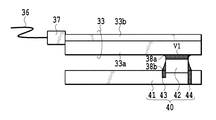
- FIG. 5A and 5B are diagrams illustrating the main part of the integrated optical module according to the first embodiment.
- FIG. 5A is a side sectional view showing a schematic configuration of a main part of the integrated optical module of the first embodiment
- FIG. 5B is a top view of a mount used in the integrated optical module of the first embodiment. is there.
- An integrated optical module is configured by mounting optical components such as a PLC chip, a lens, a light receiving element, or a light emitting element on a base substrate via a mount and sealing them with a package.
- the PLC chip 33 on which the optical interference circuit is formed is connected to an optical fiber 36 via a fiber fixing component 37, and is adhesively fixed to the mount 40 with an adhesive 38a.
- the PLC chip 33 is configured by laminating a quartz glass layer 33b in which a waveguide type optical functional circuit including a core and a clad is formed on a Si substrate 33a.
- the adhesive 38 may be, for example, a thermosetting epoxy adhesive, a humidity curable adhesive, or an oxygen curable adhesive.
- the mount 40 can be made of a metal such as Kovar.
- the mount 40 includes a flat plate-like support portion 41 to be mounted on the base substrate, a pedestal 42 formed to protrude from a part of the upper surface of the flat plate-like support portion 41, and a support portion 41 around the pedestal 42. And a groove portion 43 provided on the surface.
- An adhesive 38a is applied to the adhesive surface, which is the upper surface of the pedestal 42 of the mount 40, and the PLC chip 33 is bonded and fixed on a part of the lower surface thereof.
- a groove 43 is formed around a pedestal 42 formed in a part of the mount 40, and the adhesive 38b overflowing from the bonding surface between the PLC chip 33 and the mount 40 is accommodated. Yes.
- the adhesive is made of resin, and only the adhesive swells when the humidity increases.
- the adhesive 38 b overflowing from the adhesive surface is accommodated in the groove 43, so that the overflowing adhesive 38 b does not swell and exerts no pressure to push up the PLC chip 33. Therefore, the PLC chip 33 is not displaced and peeled off.
- the volume V2 of the groove 43 is determined based on the allowable amount of adhesive. For example, when the adhesive amount between the PLC chip 33 and the base 40 is larger than the amount V1 of the necessary adhesive 38a, the amount of adhesive more than double the amount of the necessary adhesive V1 is applied. However, the overflowing adhesive 38b does not exert pressure to push up the PLC chip 33.
- the groove 43 can be formed using a cutting drill.
- the groove 43 can be formed with a width of 1 mm, for example.
- the width of the groove 43 may not be constant, but it is preferable that the groove 43 is formed so as to have symmetry on the four sides around the base 42. If the width of the groove 43 is small, it is preferable because the adhesive enters by capillary action. However, the width of the groove 43 needs to be a certain size in order to accommodate a certain amount of the overflowing adhesive. On the other hand, if the width of the groove 43 is too large, the adhesive may not enter the groove 43 when the surface of the support 41 of the mount 40 has poor wettability.
- the width of the groove 43 is determined according to the relationship between the wettability of the surface of the mount 40 and the surface tension of the adhesive. Moreover, the groove part 43 does not need to be provided in the whole circumference
- the cross-sectional shape of the pedestal 42 is not limited to a quadrangular shape as shown in FIG. 5B, and can be configured in an arbitrary cross-sectional shape such as a circular shape, but the cross-sectional shape is a square as shown in FIG. 5B. Since the bonding area can be increased, the bonding with the PLC chip 33 is stabilized.
- the groove 43 is formed around the base 42 formed in a part of the mount 40, and the adhesive 38 b overflowing from the bonding surface between the PLC chip 33 and the mount 40 can be accommodated.
- the overflowing adhesive 38b swells and does not exert pressure to push up the PLC chip 33, so that the PLC chip 33 is not displaced or peeled off.
- FIG. 6A and 6B are diagrams showing the main part of the integrated optical module of the second embodiment.
- FIG. 6A is a side cross-sectional view illustrating a schematic configuration of a main part of the integrated optical module according to the second embodiment
- FIG. 6B is a top view of a mount used in the integrated optical module according to the second embodiment. is there.
- the integrated optical module of this embodiment has the same configuration as that of the integrated optical module of the first embodiment, except that a part of the groove 43 is configured as a through hole 44 that penetrates the support portion 41.
- the integrated optical module of the present embodiment by forming a part of the groove 43 in the through hole 44, it is possible to observe how far the adhesive is flowing and what kind of adhesive state it is in what amount of adhesive.
- the pedestal portion from the lateral direction from the gap between the PLC chip 33 of the module and the support portion 41 of the mount 40 in the state of the adhesive. This gap portion is a very small region of about several hundred ⁇ m, and observation was very difficult.
- the through-hole 44 can be formed using a cutting drill in the same manner as the groove 43.
- the through hole 44 may be formed in a part of each side of the groove formed on the four sides. It is preferable that the shape of the through hole 44 be the same on all four sides. This is because the occurrence of distortion can be prevented by providing symmetry.
- the adhesive surface of the mount 40 Excess adhesive can also be removed from the periphery of the bonding surface by vacuum-suctioning the through-hole 44 from the back side.
- the through hole is formed in a part of the groove 43 formed around the pedestal 42 formed in a part of the mount 40, and the PLC chip 33 and the mount 40 are formed.
- the pedestal may be bonded to the upper surface of the support part with an adhesive.
Landscapes
- Physics & Mathematics (AREA)
- General Physics & Mathematics (AREA)
- Optics & Photonics (AREA)
- Engineering & Computer Science (AREA)
- Microelectronics & Electronic Packaging (AREA)
- Optical Couplings Of Light Guides (AREA)
Abstract
湿度変化する際に、PLCチップの変位変動の発生を回避し、剥離がないようにした集積型光モジュールを提供すること。PLCチップと、上面に塗布された接着剤により前記PLCチップの下面の一部と接着固定された台座と、前記台座を支持する支持部とを備え、前記支持部の上面の前記台座の周囲に接着面となる前記台座の上面から溢れた接着剤が溜まる溝を形成したことを特徴とする集積型光モジュール。
Description
本発明は集積型光モジュールに関し、発光素子または受光素子とともに集積されて光送受信機を構成する平面型光波回路を搭載した集積型光モジュールに関する。
光通信技術の進展に伴い、光部品の開発が益々重要となっている。とりわけ、光送受信器は、伝送速度や応答速度の高速化が検討され、通信容量が拡大している。一般的な送受信器の構成は、光半導体を用いて作製される発光素子または受光素子と、出力用または入力用の光ファイバとから構成され、それらがレンズを介して光結合されている。例えば、光受信器の場合、入力側の光ファイバから出射された光は、レンズにより受光素子に結像され、直接検波(強度検波)される。
光伝送システムにおける変復調処理技術に目を転ずると、位相変調方式を用いた信号伝送が広く実用化されている。位相シフトキーイング(PSK)方式は、光の位相を変調することで信号を伝送する方法である。PSK方式は、変調の多値化などにより、従来に比べ、飛躍的な伝送容量の拡大ができる。
このようなPSK信号を受信するには、光の位相を検波する必要がある。受光素子は、信号光の強度を検波することはできるが、直接、光の位相を検波することができない。従って、光の位相を光強度に変換する手段が必要となる。そこで、光の干渉を用いることにより、位相差を検波する方法等がある。信号光と他の光(参照光)とを干渉させ、その干渉光の光強度を受光素子で検波することにより、光の位相情報を得ることが可能となる。参照光として別途用意した光源を用いるコヒーレント検波や、信号光自体を一部分岐して参照光として両者を干渉させる差動検波がある。このように、従来の強度変調方式のみを用いた光受信機とは異なり、近年のPSK方式の光受信機には、光の干渉により位相情報を強度情報に変換する光干渉回路が必要となっている。
このような光干渉回路は、平面型光波回路(PLC:Planar Light Circuit)を用いて実現できる。PLCは、量産性、低コスト性および高信頼性の面から優れた特徴をもち、様々な光干渉回路が実現可能である。実際に、PSK方式の光受信機に用いられる光干渉回路として、光遅延干渉回路、90度ハイブリッド回路等が実現され、実用化されている。このようなPLCは、標準的なフォトグラフィー法、エッチング技術およびFHD(Flame Hydrolysis Deposition)等のガラス堆積技術によって作製されている。
具体的な製造プロセスでは、最初に、Si等の基板上に、石英ガラス等を主原料とするアンダークラッド層と、そのアンダークラッド層より高い屈折率を持つコア層とを堆積させる。その後、コア層に様々なパターンの導波路を形成する。最後にオーバークラッド層によってその導波路を埋め込む。このようなプロセスにより、導波路型の光機能回路を有するPLCチップが作製される。信号光は、上述のようなプロセスを経て作製された導波路内に閉じ込められ、PLCチップ内部を伝搬する。
図1に、従来のPLCと光受信器との光接続方法を示す。PSK方式の光受信機におけるPLCと光受信器の基本的な接続方法は、図1に示すような、単純なファイバ接続である。入力端に光ファイバ3aが接続された平面型光波回路(PLC)1と、光受信器2とを、光ファイバ3bで繋ぐことにより光結合を行う。光結合に使用する光ファイバ3bの本数は、PLCから出力される出力光の数により決まる。光結合に使用する光ファイバの本数が、複数本になる場合もある。従って、このような光ファイバ接続を用いた光受信機の構成では、サイズが大きくなるという問題があった。そこで、PLCの出力と光受信器の入力とを、光ファイバを介さず直接的に光結合し、全体を1つのパッケージに集積することにより、光受信機を小型化できる。このような、PLCと光受信器とが直接的に光結合された形態の光受信機を、集積型光モジュールと呼ぶ。
集積型光モジュールを実現するためには、PLCチップの固定方法が特に重要となる。PLCチップから出力される光を空間中に伝搬させ、レンズ等により受光素子に光結合する場合、PLCチップからの光の出射端、レンズ、受光素子の位置関係が変化すると、全ての光を受光素子により受光できなくなり、損失となる。特に、環境温度が変化して,光受信機を納めるパッケージの温度、それぞれの素子温度等が変化した場合、熱膨張の影響によりこれらの位置が変動するため、このような損失の問題が顕著になる。低損失な光結合を実現するためには、環境温度等が変化した場合でも、それぞれの位置関係が、少なくとも相対的に、変動しないことが必要となる。
特に、PLCチップは、光受信機の中で占める面積が、受光素子に比べて1桁から2桁程度大きく、熱膨張による形状の変化が大きい。また、平面型光波回路を構成する基板と堆積された薄膜ガラスとは、大きな熱膨張係数差を持つため、温度変化によって大きなそりが発生する。このため、受光素子に対するPLCチップからの出射光の位置変位および出射角度変化が非常に問題となる。これらの2つの変化により平面型光波回路からの出射光の位置や角度が変化し、光軸ズレが発生する。光軸ズレは受光素子への光結合を劣化させ、損失を発生する。集積型光モジュールの実現には、このような光軸ズレを解消すること、もしくは、無害化することが重要である。
図2に、従来の集積型光モジュールの内部構造を示す。上述したような、温度変化による光軸ズレが発生しないように、PLCチップの底面のほぼ全面を、しっかりと固定する方法が知られている。図2に示した集積型光モジュールでは、光機能回路として光干渉回路が形成されたPLCチップ13と、レンズ14と、受光素子15とは、それぞれ固定用マウント12a,12b,12cを支持部材として、ベース基板11に固定されている。光ファイバ16とPLCチップ13とは、光ファィバ固定部品17を介して接続されている。集積型光モジュールでは、光ファイバ16から入力された光は、PLCチップ13において干渉したのち、レンズ14により受光素子15に結合する。
固定用マウント12aとPLCチップ13とは、接着剤18または半田により固定される。PLCチップ13の底面のほぼ全面を、しっかりと固定用マウントに固定することにより、温度による膨張やそり変化を抑えている。また、レンズ14、受光素子15も固定用マウントに固定することにより、温度変化による光軸ズレが発生しないようにしている。
しかしながら、図2に示す構成では、温度変化による光軸ズレは十分小さくなるように抑制できるが、一方で、温度変化によるPLCチップの特性変化が顕著になる。上述のように、平面型光波回路13は、大きな熱膨張係数差を持つSi基板13aと石英ガラス層13bとから構成されているため、温度変化によるそり変化や、熱膨張が大きい。図2に示すような構成では、PLCチップ13の底面が全面固定されているため、熱膨張やそり変化が抑制される。
一方で、この場合、大きな熱応力がSi基板13aと石英ガラス層13bとの間に発生する。応力は、光弾性効果を通じて、石英ガラス層13b内部に屈折率変化を引き起こす。PLCチップ13内に構成された光干渉回路は、干渉特性を制御するために、導波路の長さと屈折率が正確に調整されている。応力を介して発生する屈折率変化は、等価回路長の変化をもたらし、干渉計の特性を変化させるため、光干渉回路の特性を劣化させる。
これに対して、熱応力の発生を抑制することにより光学特性の変化を抑制するために、接着剤18として、弾性接着剤、ペーストなどの柔らかい接着剤、または固定用ペーストを用いたとすると(例えば、特許文献1参照)、前述の光軸ズレの影響が顕著となり、損失が発生する。
以上の問題を解決するために、PLCチップ等の光部品を集積した集積型光モジュールとして、図3に示す構成を採用することが提案されている。この構成では、固定用マウント32aの一部を隆起させて形成した台座上に接着剤38を塗布してPLCチップ33を接着固定している。図3のその他の構成は、図2と同様に構成されている。すなわち、光ファイバ36が光ファイバ固定部品37を用いてPLCチップ33に接続され、PLCチップ33、レンズ34、受光素子35等の光部品が、ベース基板31に対して、固定用マウント32a、32b、32cを介して搭載されている。この構成により、温度変化によりPLCチップに歪や反りが発生しても、光機能回路の部分は応力の影響が最小限で済み、光機能回路の特性劣化を抑制することができる。
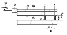
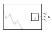
しかしながら、この集積型光モジュールではPLCチップ33とマウント40の台座部分42とを接続するために塗布した接着剤38の塗布量が多すぎると、図4Aに示すように、接着剤38が台座部分42の周囲に溢れた状態で硬化する。溢れた接着剤38はその接着力によって台座の周囲に集中して存在しやすく、マウントに広がらずに溢れた接着面の周囲に溜まってしまう。図4Bはマウントの上面図である。図4Bに示すように、断面が四角形の台座42がマウントの一部に設けられているので、台座の4辺に溢れた接着剤が溜まる。台座42とPLCチップ33との接着面が非常に小さいため、接着剤の量を正確に制御するためにはμl単位の制御をする必要がある。また一般に、金属は湿度変化に対して体積変化は大きくないが、樹脂は湿度変化に対する体積変化が大きい。湿度が変化したときに、樹脂で構成される接着剤38は膨潤するが、金属で構成されるマウント40の台座42は体積変化しない。したがって、接着面の周囲に溢れた接着剤が溜まったまま湿度変化すると、溢れた接着剤38が膨潤して、PLCチップ33を上方に押し上げる力Fを生じ、PLCチップの変位変動・剥離の原因となっていた。なお、本明細書において台座の断面とはマウント40の支持部41の上面から見た断面のことをいう。
以上に鑑み、本発明の課題は、湿度変化する際に、PLCチップの変位変動の発生を回避し、剥離がないようにした集積型光モジュールを提供することにある。
上記の課題を解決するために、一実施形態に記載された発明は、PLCチップと、上面に塗布された接着剤により前記PLCチップの下面の一部と接着固定された台座と、前記台座を支持する支持部とを備え、前記支持部の上面の前記台座の周囲に接着面となる前記台座の上面から溢れた接着剤が溜まる溝を形成したことを特徴とする集積型光モジュールである。
上記の集積型光モジュールであって、前記溝の一部は支持部の上面から下面に貫通した貫通孔を有することが好ましい。
上記の集積型光モジュールであって、前記溝の形状は、台座の周囲において対称性を有することが好ましい。
以下、本発明の実施の形態について、詳細に説明する。
(第1の実施形態)
図5A、Bは、第1の実施形態の集積型光モジュールの要部を示す図である。図5Aは、第1の実施形態の集積型光モジュールの要部の概略構成を示す側面断面図であり、図5Bは、第1の実施形態の集積型光モジュールに用いられるマウントの上面図である。集積型光モジュールは、PLCチップ、レンズ、受光素子または発光素子等の光部品を、マウントを介してベース基板上に搭載し、これらをパッケージで封止して構成される。光干渉回路が形成されたPLCチップ33は図5Aに示すように、光ファイバ36とファイバ固定部品37を介して接続され、接着剤38aによってマウント40に接着固定されている。
図5A、Bは、第1の実施形態の集積型光モジュールの要部を示す図である。図5Aは、第1の実施形態の集積型光モジュールの要部の概略構成を示す側面断面図であり、図5Bは、第1の実施形態の集積型光モジュールに用いられるマウントの上面図である。集積型光モジュールは、PLCチップ、レンズ、受光素子または発光素子等の光部品を、マウントを介してベース基板上に搭載し、これらをパッケージで封止して構成される。光干渉回路が形成されたPLCチップ33は図5Aに示すように、光ファイバ36とファイバ固定部品37を介して接続され、接着剤38aによってマウント40に接着固定されている。
PLCチップ33は、Si基板33a上に、コア、クラッドからなる導波路型の光機能回路が形成された石英ガラス層33bが積層されて構成されている。接着剤38は、例えば、熱硬化型エポキシ系の接着剤、湿度硬化型の接着剤、酸素硬化型の接着剤のいずれでもよい。
マウント40は、Kovar等の金属で構成することができる。マウント40は、ベース基板上に搭載するための平板状の支持部41と、平板状の支持部41の上面の一部に隆起して形成された台座42と、台座42の周囲の支持部41に設けられた溝部43とを備えている。マウント40の台座42の上面である接着面には、接着剤38aが塗布され、PLCチップ33がその下面の一部において接着固定されている。本発明の集積型光モジュールでは、マウント40の一部に形成された台座42の周囲に溝部43を形成して、PLCチップ33とマウント40との接着面から溢れた接着剤38bを収容している。マウント40は金属で構成されている一方、接着剤は樹脂で構成されており、湿度が高くなった場合に接着剤のみが膨潤することとなる。この台座42の周囲に溝部43を形成したことにより、接着面から溢れた接着剤38bが溝部43に収容されるので溢れた接着剤38bが膨潤してPLCチップ33を押し上げる圧力を及ぼさない。したがって、PLCチップ33が変位変動・剥離するということがない。
この溝部43の容積V2は、許容する接着剤量に基づいて決定される。例えば、PLCチップ33と台座40との間の接着面において必要な接着剤38aの量V1よりも大きくすることで、必要な接着剤の量V1よりも倍量以上の接着剤が塗布された場合でも、溢れた接着剤38bがPLCチップ33を押し上げる圧力を及ぼすことがない。
溝部43は、切削ドリルを用いて形成することができる。溝部43は例えば1mmの幅に形成できる。溝部43の幅は一定でなくてもよいが、台座42の周囲の4辺で対称性を備えるように形成することが好ましい。溝部43の幅は小さければ毛細管現象で接着剤が入り込むので好ましい。しかしながら溝部43の幅は、溢れた接着剤をある程度の量収容するためにはある程度の大きさが必要である。一方で溝部43の幅が大きすぎると、マウント40の支持部41の表面の濡れ性が悪い場合は接着剤が溝部43に入り込まない場合がある。したがって、溝部43の幅は、マウント40の表面の濡れ性と接着剤の表面張力との関係に応じて決定される。また、溝部43は、台座42の周囲の全部に設ける必要がなく、周囲の4つの辺においてそれぞれ一部のみに溝部43を設けてもよい。この場合、4つの辺で溝部43の形状が対称性を有するように設けることが好ましい。
なお、台座42の断面形状は、図5Bに示すように、四角形であることに限定されず、円形等の任意の断面形状に構成することができるが、図5Bのように断面が四角形であると、接着面積を大きく取ることができるのでPLCチップ33との接着が安定する。
このように本実施形態によれば、マウント40の一部に形成された台座42の周囲に溝部43を形成して、PLCチップ33とマウント40との接着面から溢れた接着剤38bを収容できるようにしたことにより、溢れた接着剤38bが膨潤してPLCチップ33を押し上げる圧力を及ぼさないので、PLCチップ33が変位変動・剥離するということがない。
(第2の実施形態)
図6A、Bは第2の実施形態の集積型光モジュールの要部を示す図である。図6Aは、第2の実施形態の集積型光モジュールの要部の概略構成を示す側面断面図であり、図6Bは、第2の実施形態の集積型光モジュールに用いられるマウントの上面図である。この実施形態の集積型光モジュールは、溝部43の一部が支持部41を貫通する貫通孔44として構成された以外は、第1の実施形態の集積型光モジュールと同様の構成である。
図6A、Bは第2の実施形態の集積型光モジュールの要部を示す図である。図6Aは、第2の実施形態の集積型光モジュールの要部の概略構成を示す側面断面図であり、図6Bは、第2の実施形態の集積型光モジュールに用いられるマウントの上面図である。この実施形態の集積型光モジュールは、溝部43の一部が支持部41を貫通する貫通孔44として構成された以外は、第1の実施形態の集積型光モジュールと同様の構成である。
本実施形態の集積型光モジュールでは、溝部43の一部を貫通孔44に構成することにより、接着剤がどこまで流れているか、どのぐらいの接着剤量でどういう接着状態となるかが観察できる。因みに従来のモジュールでは、接着剤の状態はモジュールのPLCチップ33とマウント40の支持部41との間のすきまから台座部分を部分横方向から観察する必要があった。このすきま部分は約数百μmという非常に小さい領域であり、観察が非常に困難であった。
貫通孔44は、溝43と同様に、切削ドリルを用いて形成することができる。貫通孔44は、4つの辺に形成された溝のそれぞれの辺のうちの一部に形成してもよい。貫通孔44の形状を四辺で同じにすることが好ましい。対称性を備えることにより、ゆがみの発生を防止できるからである。
また、貫通孔44を設ければ、溝部43の幅が大きすぎたり、マウント40の濡れ性が悪かったりして、溢れた接着剤が溝部43に入り込まない場合でも、マウント40の接着面とは裏面側から貫通孔44を真空吸引することで余分な接着剤を接着面の周囲から除去することもできる。
このように、本実施形態の構成によれば、マウント40の一部に形成された台座42の周囲に形成された溝部43の一部に貫通孔を形成して、PLCチップ33とマウント40との接着面から溢れた接着剤38bを収容できるようにしたことにより、溢れた接着剤38が膨潤してPLCチップ33を押し上げる圧力を及ぼさないので、PLCチップ33が変位変動・剥離するということがない。
以上の実施形態では、マウントを構成する支持部と台座とを一体で構成した場合を例に挙げて説明しているが、支持部の上面に台座を接着剤で接着してもよい。
33 PLCチップ
33a Si基板
33b 石英ガラス層
36 光ファイバ
37 ファイバ固定部品
38a、38b 接着剤
40 マウント
41 支持部
42 台座
43 溝部
44 貫通孔
33a Si基板
33b 石英ガラス層
36 光ファイバ
37 ファイバ固定部品
38a、38b 接着剤
40 マウント
41 支持部
42 台座
43 溝部
44 貫通孔
Claims (3)
- PLCチップと、
上面に塗布された接着剤により前記PLCチップの下面の一部と接着固定された台座と、
前記台座を支持する支持部とを備え、
前記支持部の上面の前記台座の周囲に接着面となる前記台座の上面から溢れた接着剤が溜まる溝を形成したことを特徴とする集積型光モジュール。 - 前記溝の一部は支持部の上面から下面に貫通した貫通孔を有することを特徴とする請求項1に記載の集積型光モジュール。
- 前記溝の形状は、台座の周囲において対称性を有することを特徴とする請求項1または2に記載の集積型光モジュール。
Priority Applications (2)
| Application Number | Priority Date | Filing Date | Title |
|---|---|---|---|
| US14/416,244 US20150192736A1 (en) | 2012-07-26 | 2013-07-26 | Integrated optical module |
| EP13823879.5A EP2878982B1 (en) | 2012-07-26 | 2013-07-26 | Integrated optical module |
Applications Claiming Priority (2)
| Application Number | Priority Date | Filing Date | Title |
|---|---|---|---|
| JP2012166086A JP5785139B2 (ja) | 2012-07-26 | 2012-07-26 | 集積型光モジュール |
| JP2012-166086 | 2012-07-26 |
Publications (1)
| Publication Number | Publication Date |
|---|---|
| WO2014017109A1 true WO2014017109A1 (ja) | 2014-01-30 |
Family
ID=49874375
Family Applications (1)
| Application Number | Title | Priority Date | Filing Date |
|---|---|---|---|
| PCT/JP2013/004569 Ceased WO2014017109A1 (ja) | 2012-07-26 | 2013-07-26 | 集積型光モジュール |
Country Status (5)
| Country | Link |
|---|---|
| US (1) | US20150192736A1 (ja) |
| EP (1) | EP2878982B1 (ja) |
| JP (1) | JP5785139B2 (ja) |
| CN (2) | CN103576255B (ja) |
| WO (1) | WO2014017109A1 (ja) |
Families Citing this family (5)
| Publication number | Priority date | Publication date | Assignee | Title |
|---|---|---|---|---|
| JP6528643B2 (ja) | 2015-10-27 | 2019-06-12 | 三菱電機株式会社 | 波長多重光通信モジュール |
| JP6813680B2 (ja) * | 2017-06-07 | 2021-01-13 | 日本電信電話株式会社 | 光導波路チップの接続構造 |
| JP7421840B2 (ja) * | 2019-02-08 | 2024-01-25 | 古河電気工業株式会社 | 光モジュール |
| CN110596830A (zh) * | 2019-09-24 | 2019-12-20 | 武汉光迅科技股份有限公司 | 一种光学组件 |
| CN113671638A (zh) * | 2021-07-12 | 2021-11-19 | 武汉英飞光创科技有限公司 | 一种光模块 |
Citations (6)
| Publication number | Priority date | Publication date | Assignee | Title |
|---|---|---|---|---|
| JP2003255196A (ja) * | 2002-02-27 | 2003-09-10 | Kyocera Corp | 光モジュール及びその組立方法 |
| JP2006243391A (ja) * | 2005-03-03 | 2006-09-14 | Nippon Telegr & Teleph Corp <Ntt> | 平面光波回路モジュール |
| JP2008134662A (ja) * | 2008-02-15 | 2008-06-12 | Nippon Telegr & Teleph Corp <Ntt> | 平面光回路部品及びその作製方法 |
| JP2008164828A (ja) * | 2006-12-27 | 2008-07-17 | Nippon Electric Glass Co Ltd | 光デバイス及びその光軸調整方法 |
| JP2009175364A (ja) | 2008-01-23 | 2009-08-06 | Nippon Telegr & Teleph Corp <Ntt> | 光モジュール |
| JP2011248048A (ja) * | 2010-05-26 | 2011-12-08 | Kyocera Corp | 光ファイバピグテールおよびそれを用いた光モジュール |
Family Cites Families (14)
| Publication number | Priority date | Publication date | Assignee | Title |
|---|---|---|---|---|
| JP2594813Y2 (ja) * | 1991-09-13 | 1999-05-10 | 旭光学工業株式会社 | 接着部材 |
| JPH0792342A (ja) * | 1993-07-29 | 1995-04-07 | Sumitomo Electric Ind Ltd | 光導波路モジュール |
| JPH10506204A (ja) * | 1994-09-26 | 1998-06-16 | シーメンス アクチエンゲゼルシヤフト | Oeicモジュールおよび光ファイバを光学的に相互結合するための結合装置 |
| FR2732124B1 (fr) * | 1995-03-24 | 1997-04-30 | Asulab Sa | Cellule electrique du type comprenant deux lames ou substrats paralleles, notamment en matiere plastique, ecartes l'un de l'autre par un cadre de scellement |
| US5669997A (en) * | 1995-07-13 | 1997-09-23 | Hughes Danbury Optical Systems, Inc. | Method of bonding optical members together |
| JP3264801B2 (ja) * | 1995-09-13 | 2002-03-11 | アルプス電気株式会社 | 磁気記録再生装置のヘッド移送機構 |
| US5758950A (en) * | 1996-03-05 | 1998-06-02 | Ricoh Company, Ltd. | Light source device for an image forming apparatus |
| US6327289B1 (en) * | 1997-09-02 | 2001-12-04 | Matsushita Electric Industrial Co., Ltd. | Wavelength-variable semiconductor laser, optical integrated device utilizing the same, and production method thereof |
| JP3073059U (ja) * | 2000-05-09 | 2000-11-14 | 船井電機株式会社 | レンズホルダ |
| KR100389837B1 (ko) * | 2001-07-24 | 2003-07-02 | 삼성전자주식회사 | 광도파로 소자의 패키징 장치 |
| US6970628B2 (en) * | 2004-04-15 | 2005-11-29 | Inplane Photonics, Inc. | Active optical alignment and attachment thereto of a semiconductor optical component with an optical element formed on a planar lightwave circuit |
| US8983252B2 (en) * | 2007-11-15 | 2015-03-17 | Nippon Telegraph And Telephone Corporation | Optical circuit and optical signal processing apparatus using the same |
| JP5762277B2 (ja) * | 2011-12-27 | 2015-08-12 | 株式会社フジクラ | 光フェルール及び光コネクタ |
| US9753233B2 (en) * | 2015-03-27 | 2017-09-05 | Alcatel-Lucent Usa Inc. | Method and apparatus for making an optical fiber array |
-
2012
- 2012-07-26 JP JP2012166086A patent/JP5785139B2/ja active Active
-
2013
- 2013-07-26 EP EP13823879.5A patent/EP2878982B1/en active Active
- 2013-07-26 CN CN201310320331.9A patent/CN103576255B/zh active Active
- 2013-07-26 WO PCT/JP2013/004569 patent/WO2014017109A1/ja not_active Ceased
- 2013-07-26 US US14/416,244 patent/US20150192736A1/en not_active Abandoned
- 2013-07-26 CN CN201320453700.7U patent/CN203385901U/zh not_active Expired - Lifetime
Patent Citations (6)
| Publication number | Priority date | Publication date | Assignee | Title |
|---|---|---|---|---|
| JP2003255196A (ja) * | 2002-02-27 | 2003-09-10 | Kyocera Corp | 光モジュール及びその組立方法 |
| JP2006243391A (ja) * | 2005-03-03 | 2006-09-14 | Nippon Telegr & Teleph Corp <Ntt> | 平面光波回路モジュール |
| JP2008164828A (ja) * | 2006-12-27 | 2008-07-17 | Nippon Electric Glass Co Ltd | 光デバイス及びその光軸調整方法 |
| JP2009175364A (ja) | 2008-01-23 | 2009-08-06 | Nippon Telegr & Teleph Corp <Ntt> | 光モジュール |
| JP2008134662A (ja) * | 2008-02-15 | 2008-06-12 | Nippon Telegr & Teleph Corp <Ntt> | 平面光回路部品及びその作製方法 |
| JP2011248048A (ja) * | 2010-05-26 | 2011-12-08 | Kyocera Corp | 光ファイバピグテールおよびそれを用いた光モジュール |
Non-Patent Citations (1)
| Title |
|---|
| See also references of EP2878982A4 |
Also Published As
| Publication number | Publication date |
|---|---|
| EP2878982A4 (en) | 2016-03-30 |
| CN203385901U (zh) | 2014-01-08 |
| US20150192736A1 (en) | 2015-07-09 |
| CN103576255A (zh) | 2014-02-12 |
| EP2878982B1 (en) | 2019-04-10 |
| CN103576255B (zh) | 2017-04-12 |
| EP2878982A1 (en) | 2015-06-03 |
| JP2014026105A (ja) | 2014-02-06 |
| JP5785139B2 (ja) | 2015-09-24 |
Similar Documents
| Publication | Publication Date | Title |
|---|---|---|
| JP5922042B2 (ja) | 光モジュール | |
| US9116317B2 (en) | Planar lightwave circuit | |
| US8827572B2 (en) | Side coupling optical fiber assembly and fabrication method thereof | |
| US9235001B2 (en) | Optical device and optical module | |
| US20180259730A1 (en) | Photonic interface for electronic circuit | |
| US9116291B2 (en) | Integrated optical module | |
| JP5779339B2 (ja) | 光モジュール | |
| JP5785139B2 (ja) | 集積型光モジュール | |
| JP2018010030A (ja) | 光モジュール | |
| JP5918648B2 (ja) | 集積型光モジュール | |
| KR101416638B1 (ko) | 평면 광도파로의 광신호 모니터링 장치 | |
| JP4504435B2 (ja) | 平面光回路部品及びその作製方法 | |
| WO2022254657A1 (ja) | 集積型光デバイスおよびその製造方法 | |
| JP2024123676A (ja) | 光デバイス、光送信装置及び光受信装置 | |
| JP2007206318A (ja) | 一芯双方向光通信モジュール | |
| JP2009020425A (ja) | 光導波路保持部材及び光トランシーバ |
Legal Events
| Date | Code | Title | Description |
|---|---|---|---|
| 121 | Ep: the epo has been informed by wipo that ep was designated in this application |
Ref document number: 13823879 Country of ref document: EP Kind code of ref document: A1 |
|
| WWE | Wipo information: entry into national phase |
Ref document number: 14416244 Country of ref document: US |
|
| WWE | Wipo information: entry into national phase |
Ref document number: 2013823879 Country of ref document: EP |
|
| NENP | Non-entry into the national phase |
Ref country code: DE |