WO2014017363A1 - 光学シート及び面光源装置 - Google Patents
光学シート及び面光源装置 Download PDFInfo
- Publication number
- WO2014017363A1 WO2014017363A1 PCT/JP2013/069450 JP2013069450W WO2014017363A1 WO 2014017363 A1 WO2014017363 A1 WO 2014017363A1 JP 2013069450 W JP2013069450 W JP 2013069450W WO 2014017363 A1 WO2014017363 A1 WO 2014017363A1
- Authority
- WO
- WIPO (PCT)
- Prior art keywords
- light
- layer
- optical sheet
- particles
- adhesive layer
- Prior art date
- Legal status (The legal status is an assumption and is not a legal conclusion. Google has not performed a legal analysis and makes no representation as to the accuracy of the status listed.)
- Ceased
Links
Images

Classifications
-
- G—PHYSICS
- G02—OPTICS
- G02B—OPTICAL ELEMENTS, SYSTEMS OR APPARATUS
- G02B5/00—Optical elements other than lenses
- G02B5/02—Diffusing elements; Afocal elements
- G02B5/0205—Diffusing elements; Afocal elements characterised by the diffusing properties
- G02B5/0236—Diffusing elements; Afocal elements characterised by the diffusing properties the diffusion taking place within the volume of the element
- G02B5/0242—Diffusing elements; Afocal elements characterised by the diffusing properties the diffusion taking place within the volume of the element by means of dispersed particles
-
- F—MECHANICAL ENGINEERING; LIGHTING; HEATING; WEAPONS; BLASTING
- F21—LIGHTING
- F21V—FUNCTIONAL FEATURES OR DETAILS OF LIGHTING DEVICES OR SYSTEMS THEREOF; STRUCTURAL COMBINATIONS OF LIGHTING DEVICES WITH OTHER ARTICLES, NOT OTHERWISE PROVIDED FOR
- F21V3/00—Globes; Bowls; Cover glasses
- F21V3/04—Globes; Bowls; Cover glasses characterised by materials, surface treatments or coatings
- F21V3/06—Globes; Bowls; Cover glasses characterised by materials, surface treatments or coatings characterised by the material
-
- F—MECHANICAL ENGINEERING; LIGHTING; HEATING; WEAPONS; BLASTING
- F21—LIGHTING
- F21V—FUNCTIONAL FEATURES OR DETAILS OF LIGHTING DEVICES OR SYSTEMS THEREOF; STRUCTURAL COMBINATIONS OF LIGHTING DEVICES WITH OTHER ARTICLES, NOT OTHERWISE PROVIDED FOR
- F21V5/00—Refractors for light sources
- F21V5/002—Refractors for light sources using microoptical elements for redirecting or diffusing light
-
- G—PHYSICS
- G02—OPTICS
- G02B—OPTICAL ELEMENTS, SYSTEMS OR APPARATUS
- G02B5/00—Optical elements other than lenses
- G02B5/02—Diffusing elements; Afocal elements
- G02B5/0273—Diffusing elements; Afocal elements characterized by the use
- G02B5/0278—Diffusing elements; Afocal elements characterized by the use used in transmission
-
- H—ELECTRICITY
- H05—ELECTRIC TECHNIQUES NOT OTHERWISE PROVIDED FOR
- H05B—ELECTRIC HEATING; ELECTRIC LIGHT SOURCES NOT OTHERWISE PROVIDED FOR; CIRCUIT ARRANGEMENTS FOR ELECTRIC LIGHT SOURCES, IN GENERAL
- H05B33/00—Electroluminescent light sources
- H05B33/02—Details
-
- H—ELECTRICITY
- H10—SEMICONDUCTOR DEVICES; ELECTRIC SOLID-STATE DEVICES NOT OTHERWISE PROVIDED FOR
- H10K—ORGANIC ELECTRIC SOLID-STATE DEVICES
- H10K50/00—Organic light-emitting devices
- H10K50/10—OLEDs or polymer light-emitting diodes [PLED]
- H10K50/11—OLEDs or polymer light-emitting diodes [PLED] characterised by the electroluminescent [EL] layers
-
- H—ELECTRICITY
- H10—SEMICONDUCTOR DEVICES; ELECTRIC SOLID-STATE DEVICES NOT OTHERWISE PROVIDED FOR
- H10K—ORGANIC ELECTRIC SOLID-STATE DEVICES
- H10K50/00—Organic light-emitting devices
- H10K50/80—Constructional details
- H10K50/85—Arrangements for extracting light from the devices
- H10K50/854—Arrangements for extracting light from the devices comprising scattering means
-
- H—ELECTRICITY
- H10—SEMICONDUCTOR DEVICES; ELECTRIC SOLID-STATE DEVICES NOT OTHERWISE PROVIDED FOR
- H10K—ORGANIC ELECTRIC SOLID-STATE DEVICES
- H10K50/00—Organic light-emitting devices
- H10K50/80—Constructional details
- H10K50/85—Arrangements for extracting light from the devices
- H10K50/858—Arrangements for extracting light from the devices comprising refractive means, e.g. lenses
-
- G—PHYSICS
- G02—OPTICS
- G02B—OPTICAL ELEMENTS, SYSTEMS OR APPARATUS
- G02B5/00—Optical elements other than lenses
- G02B5/02—Diffusing elements; Afocal elements
- G02B5/0205—Diffusing elements; Afocal elements characterised by the diffusing properties
- G02B5/021—Diffusing elements; Afocal elements characterised by the diffusing properties the diffusion taking place at the element's surface, e.g. by means of surface roughening or microprismatic structures
- G02B5/0226—Diffusing elements; Afocal elements characterised by the diffusing properties the diffusion taking place at the element's surface, e.g. by means of surface roughening or microprismatic structures having particles on the surface
-
- H—ELECTRICITY
- H10—SEMICONDUCTOR DEVICES; ELECTRIC SOLID-STATE DEVICES NOT OTHERWISE PROVIDED FOR
- H10K—ORGANIC ELECTRIC SOLID-STATE DEVICES
- H10K2102/00—Constructional details relating to the organic devices covered by this subclass
- H10K2102/301—Details of OLEDs
- H10K2102/331—Nanoparticles used in non-emissive layers, e.g. in packaging layer
-
- H—ELECTRICITY
- H10—SEMICONDUCTOR DEVICES; ELECTRIC SOLID-STATE DEVICES NOT OTHERWISE PROVIDED FOR
- H10K—ORGANIC ELECTRIC SOLID-STATE DEVICES
- H10K50/00—Organic light-emitting devices
- H10K50/80—Constructional details
- H10K50/84—Passivation; Containers; Encapsulations
- H10K50/841—Self-supporting sealing arrangements
Definitions
- the present invention relates to a surface light source device including an optical sheet and an organic electroluminescence (hereinafter referred to as “organic EL”) element.
- organic EL organic electroluminescence
- An organic EL element in which an organic light emitting layer is provided between a plurality of electrodes to obtain light emission has been studied for use as a display element instead of a liquid crystal cell.
- an organic EL device as a surface light source device such as a flat illumination and a backlight for a liquid crystal display device, which takes advantage of its high luminous efficiency, low voltage drive, light weight, and low cost, is also being studied. .
- an organic EL element When using an organic EL element as a light source of a surface light source device, it is a problem to extract useful light from the element with high efficiency.
- the light emitting layer of the organic EL element itself has high luminous efficiency, depending on conditions such as the difference in refractive index between the layers constituting the element, the loss of light until the light is transmitted through the layer and emitted is large. Become. Therefore, it is required to reduce such light loss as much as possible.
- Patent Document 1 As a method for increasing the light extraction efficiency, it is known to provide an optical sheet having a plurality of layers having predetermined optical characteristics on the light extraction surface side of the light source device (for example, Patent Document 1). By providing such an optical sheet, it is expected that the light extraction efficiency is improved and the change in color depending on the observation angle is reduced.
- high refractive glass As a substrate, it is expected that the light extraction efficiency from the light emitting layer having a high refractive index of about 1.8 to the substrate is increased.
- a high refractive glass substrate it becomes difficult to emit light from there to another layer or the outside of the device.
- an optical sheet in which the layer directly in contact with the glass substrate has light diffusibility.
- an optical sheet having a transparent substrate and an adhesive layer the adhesive layer having a high refractive index and light diffusibility.
- an object of the present invention is to increase the light extraction efficiency of the surface light source device, reduce the change in color depending on the observation angle, and reduce the occurrence of surface unevenness, and the light extraction efficiency.
- An object of the present invention is to provide a surface light source device that is high, has a low color change due to an observation angle, and has little surface unevenness.
- an optical sheet having a light diffusion layer having a predetermined characteristic in addition to the light diffusion adhesive layer That is, an optical sheet in which a light diffusion layer is provided on one surface side of a transparent substrate and a light diffusion adhesive layer is provided on the other surface side, and the light diffusion layer has a predetermined haze. It has been found that the use of a material can reduce the visibility of planar unevenness caused by unevenness of the light diffusing adhesive layer while increasing the light extraction efficiency by the light diffusing adhesive layer, and has completed the present invention. That is, according to the present invention, the following [1] to [7] are provided.
- An optical sheet having The light diffusion layer includes a resin and first diffusion particles having a number average particle diameter of 1.7 ⁇ m or more,
- the light diffusing adhesive layer comprises a binder, highly refractive nanoparticles and second diffusing particles;
- the optical sheet in which the haze x1 (%) of the light diffusing layer and the haze x2 (%) of the light diffusing adhesive layer satisfy a relationship of x1> x2.
- the high-refractive nanoparticles are particles made of an inorganic material or particles made of an inorganic material and an organic film covering the outer surface, and the second diffusion particles are particles made of an organic material.
- the refractive index n2 of the second diffusing particles and the refractive index n1 of the remaining components of the light diffusing adhesive layer satisfy the relationship n1> n2.
- a surface light source device comprising the optical sheet according to any one of [1] to [6] and an organic electroluminescence light emitting element.
- the optical sheet of the present invention can increase the light extraction efficiency of the surface light source device, can reduce the change in color depending on the observation angle, and can reduce the occurrence of surface unevenness.
- the surface light source device of the present invention has high light extraction efficiency, low change in color depending on the observation angle, and little surface unevenness.
- FIG. 1 is a cross-sectional view schematically showing an example of the optical sheet of the present invention.
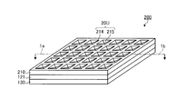
- FIG. 2 is a perspective view schematically showing another example of the optical sheet of the present invention.
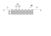
- 3 is a cross-sectional view showing a cross section of the optical sheet shown in FIG. 2 cut along a plane passing through line 1a-1b in FIG. 2 and perpendicular to the plane direction of the transparent substrate.
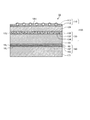
- FIG. 4 is a cross-sectional view schematically showing an example of the surface light source device of the present invention.
- the optical sheet of the present invention comprises a transparent substrate, a light diffusion layer provided on one surface of the transparent substrate, and a light diffusion adhesive layer provided on the other surface of the transparent substrate.
- FIG. 1 is a cross-sectional view schematically showing an example of the optical sheet of the present invention.
- the optical sheet 100 is in direct contact with the transparent base material 121, the light diffusion layer 110 provided in direct contact with one surface of the transparent base material 121, and the other surface of the transparent base material 121.
- a light diffusion adhesive layer 130 provided.
- the light diffusing layer and the light diffusing adhesive layer are directly provided on the surface of the transparent substrate, but the optical sheet of the present invention is not limited to such an embodiment, and the transparent substrate and the light diffusing layer or the light diffusing layer. Another layer may be interposed between the adhesive layer.
- the light diffusion layer 110 includes a resin 112 and first diffusion particles 113, and the surface 10 ⁇ / b> U has an uneven structure due to the presence of the first diffusion particles 113.
- the light diffusing adhesive layer includes a binder 132, second diffusing particles 133, and highly refractive nanoparticles 134. Since the surface of the light diffusing adhesive layer 130 is an adhesive surface, it can be stored with the separator 141 attached as necessary, and can be used after the separator 141 is peeled off.
- the transparent substrate is “transparent” means having a light transmittance of a degree suitable for use as a material for the optical sheet.
- each layer constituting the optical sheet can have a light transmittance suitable for use in an optical member, and the whole optical sheet has a total light transmittance of 50% or more. be able to.
- the material of the transparent substrate glass or various resins capable of forming a transparent layer can be used.
- the material for the transparent substrate include a thermoplastic resin, a thermosetting resin, an ultraviolet curable resin, and an electron beam curable resin.
- a thermoplastic resin is preferable because it is easy to process.
- thermoplastic resins include polyester-based, polyacrylate-based, and cycloolefin polymer-based resins.
- the transparent substrate is not limited to a single layer, and may be a laminate of a plurality of transparent substrates.
- the refractive index of the transparent substrate is preferably higher because the light extraction efficiency from the light diffusion adhesive layer to the transparent substrate is higher, but in the present invention, by using a specific one as the light diffusion adhesive layer, Even if the refractive index of the transparent substrate is lower than that of the light diffusion adhesive layer, good light extraction efficiency can be obtained. Therefore, the material of the transparent substrate is not limited to one having a high refractive index, and the material can be appropriately selected from the viewpoints of properties other than the refractive index and cost. Specifically, the refractive index of the transparent substrate is preferably 1.4 or more, more preferably 1.5 or more, and on the other hand, preferably 1.9 or less, and 1.7 or less. More preferably.
- the refractive index of each layer can be measured with a spectroscopic ellipsometer (manufactured by M-2000 Woollam Co., Ltd.) using a sample obtained by forming a single layer or multiple layers in a sheet form.
- the thickness of the transparent substrate is preferably 20 to 300 ⁇ m if it is made of a resin, for example.
- the thickness is preferably 10 to 1100 ⁇ m.
- the optical sheet of the present invention is called a “sheet” because it has a thin flat plate structure, but this does not necessarily require flexibility. Therefore, for example, the optical sheet of the present invention includes a laminate having 700 ⁇ m thickness as the transparent substrate and having no flexibility.
- a light-diffusion layer is a layer provided in the one surface side of a transparent base material.
- the light diffusion layer is usually located on the light exit surface side (that is, on the optical sheet, the side farther from the light emitting layer than the light diffusion adhesive layer and the transparent substrate). It is a layer to do.
- the light diffusion layer may be provided directly on the surface of the transparent substrate, but may be provided via an arbitrary layer. It is preferable to be provided directly from the viewpoint of ease of manufacture and the like.
- the light diffusion layer includes a resin and first diffusion particles having a predetermined number average particle diameter.
- thermoplastic resins examples include thermoplastic resins, thermosetting resins, and energy ray curable resins such as ultraviolet curable resins and electron beam curable resins. Of these, thermosetting resins and energy beam curable resins are preferred from the viewpoints of high hardness and production efficiency.
- thermoplastic resins include polyester, polyacrylate, and cycloolefin polymer resins.
- ultraviolet curable resins include epoxy, acrylic, urethane, ene / thiol, and isocyanate resins. As these resins, those having a plurality of polymerizable functional groups can be preferably used.
- the first diffusion particles included in the light diffusion layer may be transparent or opaque.
- the material of the first diffusion particles include metals and metal compounds, and resins.
- metal compounds include metal oxides and nitrides. Specific examples of metals and metal compounds include metals having high reflectivity such as silver and aluminum, and metal compounds such as silicon oxide, aluminum oxide, zirconium oxide, silicon nitride, tin-added indium oxide, and titanium oxide. be able to.
- examples of the resin include methacrylic resin, polyurethane resin, silicone resin, and melamine resin.
- the shape of the first diffusing particles is not particularly limited, and may be a spherical shape, a cylindrical shape, a cubic shape, a rectangular parallelepiped shape, a pyramid shape, a conical shape, a star shape, or the like.
- the first diffusion particles have a number average particle diameter of 1.7 ⁇ m or more.
- the number average particle diameter can be measured by various particle size distribution analyzers (for example, centrifugal sedimentation type particle size distribution analyzer, CAPA-700, Horiba, Ltd.).
- the number average particle diameter is at least the lower limit, it is possible to provide an uneven structure on the surface of the light diffusion layer. Since the light diffusion layer has a concavo-convex structure, the light extraction efficiency can be improved.
- the particle diameter is the diameter of a sphere having the same volume.
- the upper limit of the number average particle size of the first diffusion particles is not particularly limited, but can be 30 ⁇ m or less.
- the difference between the refractive index of the first diffusion particles and the refractive index of the resin constituting the light diffusion layer is preferably 0.05 to 0.5. 0.07 to 0.5 is more preferable.
- either the first diffusing particle or the refractive index of the resin may be larger. If the refractive index of the first diffusing particles and the resin is too close, the diffusion effect cannot be obtained and the color unevenness is not suppressed. Conversely, if the difference is too large, the diffusion becomes large and the color unevenness is suppressed, but the light extraction effect. Will be reduced.
- the blending ratio of the resin and the first diffusion particles in the light diffusion layer is preferably 3 to 50% by weight as the ratio of the first diffusion particles to the total of these.
- the light diffusion layer can contain an optional component as necessary in addition to the resin and the first diffusion particles.
- the optional component include an antistatic agent, a crosslinking agent, a UV absorber, a fluorescent agent, and a phosphorescent agent.
- the refractive index of the light diffusion layer is preferably higher than that of the transparent substrate.
- the size of the surface uneven structure of the light diffusion layer is not particularly limited, but the arithmetic average roughness Ra is preferably 0.15 ⁇ m or more.
- the lower limit of the thickness of the light diffusion layer is preferably 1 ⁇ m or more, more preferably 3 ⁇ m or more, while the upper limit thereof is preferably 50 ⁇ m or less, and 20 ⁇ m or less. It is more preferable that In particular, when the thickness is equal to or less than the above upper limit, surface irregularities based on the first diffusion particles can be satisfactorily formed.
- a light-diffusion adhesion layer is a layer provided in the surface side opposite to the surface in which the light-diffusion layer was provided of the transparent base material.
- the light diffusing adhesive layer is usually a layer located on the light incident surface side (that is, the side closer to the light emitting layer than the light diffusing layer and the transparent substrate).
- the light diffusing adhesive layer may be provided directly on the surface of the transparent substrate, or may be provided via another layer. It is preferable to be provided directly from the viewpoint of ease of manufacture and the like.
- the light diffusing adhesive layer is a light diffusing adhesive layer. That is, the light diffusion adhesive layer is a layer having a function of adhering the optical sheet to another layer of the organic EL element in addition to the function of diffusing the light transmitted through the optical sheet.
- the optical sheet of the present invention can be easily provided on the organic EL element, and the light extraction efficiency can be improved by simplifying the layer structure of the organic EL element. it can.
- the light diffusion adhesive layer contains a binder, highly refractive nanoparticles, and second diffusion particles.
- a light-diffusion adhesion layer becomes a layer which touches the board
- the substrate of the organic EL element can be made of high refractive glass in order to increase the light extraction efficiency from the light emitting element.
- the light extraction efficiency from the substrate to the light diffusion adhesive layer can be improved by the light diffusion adhesive layer containing the high refractive nanoparticles and consequently having a high refractive index.
- the light diffusion adhesive layer further includes the second diffusing particles, the light entering the light diffusion adhesive layer is diffused. As a result, even if the refractive index of the transparent substrate is not so high, the light diffusion adhesive layer The light extraction efficiency from the transparent substrate to the transparent substrate can be improved.
- the binder material included in the light diffusion adhesive layer examples include an epoxy resin, a (meth) acrylic resin, a silicone resin, a urethane resin, a polyimide resin, an acid-modified polyolefin, an aliphatic hydrocarbon resin, or a mixture thereof. it can. By using these resins, the light diffusion adhesive layer can be easily formed, and the light diffusion adhesive layer can be provided with the function as the adhesive layer.
- Examples of the high refractive nanoparticle included in the light diffusing adhesive layer include particles made of an inorganic material and particles made of an organic material having a refractive index of 1.68 or more.
- examples of inorganic materials include oxide nanoparticles such as zirconia, titania, tin oxide and zinc oxide, titanates such as barium titanate and strontium titanate; CdS, CdSe, ZnSe, CdTe, ZnS, HgS, HgSe, Examples thereof include sulfides such as PdS and SbSe, selenides, telluride nanoparticles, and the like.
- a styrene resin or the like As an example of an organic material having a refractive index of 1.68 or more, a styrene resin or the like can be given.
- the surface of these nanoparticles may be surface-modified with various functional groups for improving dispersibility, a silane coupling agent, or the like.
- the upper limit of the refractive index of the highly refractive nanoparticles is not particularly limited, but can be 3.0 or less.
- the shape of the highly refractive nanoparticles is not particularly limited, and may be a spherical shape, a cylindrical shape, a cubic shape, a rectangular parallelepiped shape, a pyramid shape, a conical shape, a star shape, or the like.
- the number-average particle diameter of the highly refractive nanoparticles is preferably 1 nm or more, more preferably 5 nm or more, on the other hand, preferably 200 nm or less, and more preferably 100 nm or less. By setting the number average particle diameter within the above range, the effect of increasing the refractive index can be favorably obtained.
- the content ratio of the high refractive nanoparticles in the light diffusing adhesive layer is preferably 20% by weight or more, and preferably 30% by weight or more as a ratio with respect to the total of the binder, the high refractive nanoparticles and the second diffusion particles. More preferably, it is preferably 80% by weight or less, more preferably 70% by weight or less.
- Examples of the material of the second diffusion particle included in the light diffusion adhesive layer include an organic material, particularly an organic material having a refractive index of less than 1.55, preferably an acrylic crosslinked particle having a refractive index of less than 1.5, and a silicone resin. And so on. More specifically, among those exemplified as the material of the second diffusing particles described above, those having characteristics such as a refractive index in a desired range can be appropriately selected and used.
- the lower limit of the refractive index of the second diffusing particles is not particularly limited, but may be 1.3 or more.
- the number average particle diameter of the second diffusion particles is preferably 0.3 ⁇ m or more, more preferably 0.5 ⁇ m or more, and on the other hand, it is preferably 1.7 ⁇ m or less, and preferably 1 ⁇ m or less. More preferred.
- the effects of the present invention can be obtained satisfactorily.
- the number average particle diameter is not more than the above upper limit because high diffusion can be obtained while suppressing an increase in haze.
- the content ratio of the second diffusing particles in the light diffusing adhesive layer is preferably 1% by weight or more, and preferably 3% by weight or more, as a ratio with respect to the total of the binder, the highly refractive nanoparticles and the second diffusing particles. More preferably, it is preferably 30% by weight or less, more preferably 20% by weight or less.
- the light diffusing adhesive layer can contain an optional component as required in addition to the binder, the high refractive nanoparticle, and the second diffusing particle.
- the optional component include various additives such as a tackifier, a curing agent, a plasticizer, and a UV absorber.
- the refractive index of the light diffusing adhesive layer can be appropriately set according to the use of the optical sheet.
- the refractive index of the light diffusion adhesive layer is preferably higher than the refractive index of the substrate.
- a lower refractive index is preferable.
- the refractive index of the transparent substrate is preferably 1.57 or more, more preferably 1.6 or more, and preferably 1.9 or less, and 1.8 or less. More preferably.
- the refractive index in such a range can be obtained mainly by adjusting the ratio of highly refractive nanoparticles.
- the refractive index n2 of the second diffusing particles and the refractive index n1 of the remaining component of the light diffusing adhesive layer satisfy the relationship n1> n2.
- the remaining components are components other than the second diffusion particles among the components constituting the light diffusion adhesive layer.
- the second diffusing particles are not added, and the other components are used in the same amount as used for the production of the light diffusing adhesive layer, and the layer is formed in the same manner as the light diffusing adhesive layer.
- the refractive index n1 of the remaining component can be determined. Or it can also be estimated based on the optical properties and blending ratios of the main components (binder and highly refractive nanoparticles) constituting the remaining components.
- the lower limit of the thickness of the light diffusing adhesive layer is preferably 1 ⁇ m or more, more preferably 10 ⁇ m or more, and can be 30 ⁇ m or more or 40 ⁇ m or more, while the upper limit is 100 ⁇ m or less. It is preferable that the thickness is 60 ⁇ m or less.
- the haze x1 (%) of the light diffusion layer and the haze x2 (%) of the light diffusion adhesive layer satisfy the relationship of x1> x2.
- Haze x1 and haze x2 can be measured by forming a light diffusion layer or a light diffusion adhesive layer to be measured on a transparent substrate and measuring the haze.
- a measuring instrument a commercially available turbidimeter (NDH-4000, manufactured by Nippon Denshoku Industries Co., Ltd.) can be used in accordance with JIS K7105.
- the light diffusion adhesive layer is required to contain a large amount of highly refractive nanoparticles and second diffusion particles.
- the viscosity of the material for forming the light diffusing adhesive layer is increased, and the degree of dispersion of the particles in the material is lowered. As a result, unevenness is likely to occur.
- haze x1 and haze x2 are not particularly limited as long as the above requirements are satisfied, but x1 is preferably 98.5% or more, more preferably 98.7% or more, while preferably 99. 0.7% or less, more preferably 99.5% or less. In particular, when x1 is equal to or more than the preferable lower limit, it is possible to satisfactorily achieve reduction in planar unevenness.
- the haze of the entire optical sheet is approximately the same as the value calculated as follows from x1 and x2. .
- Haze of optical sheet as a whole (calculated value,%) x1 + (100 ⁇ x1) * (x2 / 100)
- the haze of the entire optical sheet of the present invention is not particularly limited, but is preferably 98.5% or more, more preferably 98.7% or more, and preferably 99.7 or less, more preferably 99.5% or less. is there.
- the surface uneven structure of the light diffusing layer may be an uneven structure based on the shape of the first diffusion particles, but in addition to or instead of the uneven structure provided by a mold such as a mold. You may have.
- FIG. 2 is a perspective view schematically showing an example of the optical sheet of the present invention having such a surface uneven structure imparted by a mold
- FIG. 3 shows the optical sheet shown in FIG.
- FIG. 4 is a cross-sectional view showing a cross section cut along a plane passing through a line 1a-1b and perpendicular to the plane direction of the transparent substrate.
- the optical sheet 200 is different from the optical sheet 100 shown in FIG. 1 in that the optical sheet 200 has a light diffusing layer 210 having a surface uneven structure imparted by a mold, instead of the light diffusing layer 110 shown in FIG.
- the other points are common to the optical sheet 100.
- the light diffusion layer 210 has a concavo-convex structure including a plurality of concave portions 215 and a flat portion 214 located around the concave portions 215 on the upper surface thereof.
- the uneven structure defines the surface 20U of the optical sheet 200. Effects such as an improvement in light extraction efficiency can also be obtained by such a surface uneven structure imparted by the mold.
- the uneven structure imparted by the mold is not limited to the quadrangular pyramid depression shown in FIGS. 2 and 3, and may have other shapes.
- a pyramid shape other than a quadrangular pyramid, a conical shape, a shape of a part of a spherical surface, a groove shape, and a shape obtained by combining these shapes may be used.
- the cone and the pyramid may be not only a regular cone and pyramid with a sharp top, but also a shape with a rounded tip or a flat chamfered shape.
- the optical sheet of the present invention is prepared, for example, by preparing a coating liquid (1) suitable for forming a light diffusing layer and a coating liquid (2) suitable for forming a light diffusing adhesive layer. It can manufacture by forming a light-diffusion layer and a light-diffusion adhesion layer in each of both surfaces of a transparent base material using.
- the coating liquid (1) suitable for forming the light diffusion layer As the coating liquid (1) suitable for forming the light diffusion layer, the above-described compositions containing the resin of the material of the light diffusion layer and the first diffusion particles can be used.
- the coating liquid (1) can contain a solvent as needed. Examples of such solvents include toluene, hexane, cyclohexane, methylcyclohexane, methyl ethyl ketone, ethyl acetate, and mixtures thereof.
- the coating liquid (1) contains a resin, the first diffusing particles and a solvent, the ratio of the solvent in the entire coating liquid (1) can be 10 to 80% by weight.
- the coating liquid (1) is applied on the surface of the transparent substrate, the solvent is volatilized as necessary, and a curing process is performed by irradiation with energy rays as necessary to obtain a light diffusion layer. be able to.
- the volatilization of the solvent can be performed, for example, by heating in a predetermined temperature range for a predetermined time.
- the heating temperature is preferably 40 to 200 ° C, more preferably 40 to 140 ° C.
- the heating time is preferably 15 to 600 s.
- the surface uneven structure of the light diffusion layer can be obtained as a shape corresponding to the shape of the first diffusion particles by appropriately selecting the number average particle diameter of the first diffusion particles and the film thickness of the light diffusion layer. .
- a surface uneven structure can be imparted by preparing a mold such as a mold having a desired shape and transferring the shape of the mold at an arbitrary stage after obtaining the coating film.
- the coating liquid (2) suitable for forming the light diffusing adhesive layer As the coating liquid (2) suitable for forming the light diffusing adhesive layer, the above-described composition containing the resin of the material for the light diffusing adhesive layer, the high refractive nanoparticles, and the second diffusing particles is used. Can be used.
- the coating liquid (2) can preferably further contain a solvent. Examples of such solvents include toluene, hexane, cyclohexane, methylcyclohexane, methyl ethyl ketone, ethyl acetate, and mixtures thereof.
- the coating liquid (2) contains a resin, highly refractive nanoparticles, second diffusing particles and a solvent, the ratio of the solvent in the entire coating liquid (2) can be 30 to 85% by weight.
- the coating liquid (2) By applying the coating liquid (2) onto the surface of the transparent substrate, volatilizing the solvent as necessary, and further performing a curing treatment by irradiation with energy rays as necessary, the light diffusion adhesive layer Obtainable.
- the volatilization of the solvent can be performed, for example, by heating in a predetermined temperature range for a predetermined time.
- the heating temperature is preferably 40 to 200 ° C, more preferably 40 to 140 ° C.
- the heating time is preferably 15 to 600 s.
- a separator can be attached on the light diffusion adhesive layer as necessary.
- easy sticking can be achieved by peeling the separator immediately before sticking the optical sheet of the present invention to another layer.
- the surface light source device of the present invention includes the optical sheet of the present invention and an organic EL element.
- FIG. 4 is a cross-sectional view schematically showing an example of the surface light source device of the present invention including the optical sheet 100 of the present invention shown in FIG.
- the surface light source device 10 is a device having a plate-like structure, a substrate 151 made of a material such as glass, and the optical sheet 100 of the present invention provided in contact with the surface 15U on the device light-emitting surface side of the substrate 151; And an organic EL element 160 provided in contact with the other surface 15L of the substrate 151.
- the surface light source device 10 further includes a sealing substrate 171 provided as an optional component on the surface 16L side of the organic EL element 160 opposite to the device light exit surface.
- a high refractive index glass having a refractive index of 1.6 or more is preferably used. By using a substrate having such a high refractive index, the light extraction efficiency from the organic EL element 160 to the substrate is improved.
- the upper limit of the refractive index of the high refractive index glass is not particularly limited, but may be 2.5 or less.
- the organic EL element 160 includes a first electrode layer 161, a light emitting layer 162, and a second electrode layer 163 in order from the side close to the substrate 151.
- the first electrode layer 161 is a transparent electrode
- the second electrode layer 163 is a reflective electrode.
- the optical sheet 100 is provided such that the light diffusion layer 110 is positioned on the upper surface of the surface light source device 10 (that is, the outermost layer on the light output surface side of the surface light source device 10), and the light diffusion adhesive layer 130 is in contact with the substrate 151.
- the optical sheet 100 is adhered to the substrate 151 by the function of the light diffusion adhesive layer 130 as an adhesive layer.
- the light emitted from the organic EL element 160 toward the device light exit surface enters the substrate 151 and further enters the light diffusion adhesive layer 130.
- the light diffusion adhesive layer 130 contains the high refractive nanoparticles 134 and has a high refractive index as a whole layer, high light extraction efficiency from the substrate 151 to the light diffusion adhesive layer can be obtained.
- the light diffusion adhesive layer 130 has the second diffusion particles 133, so that the light traveling direction is diffused.
- the second diffusing particles 133 are preferably particles having a number average particle diameter of 0.3 to 1.7 ⁇ m, whereby light is diffused at a wide angle while the haze is relatively low.
- the light diffusing adhesive layer 130 may be uneven, but the haze value of the light diffusing adhesive layer 130 is a low value per se and relatively relative to the light diffusing layer 110. Since the value is low, the unevenness of the light diffusing adhesive layer 130 is less likely to affect the surface shape when observed from the device light exit surface (that is, the surface of the light diffusing layer 110) 10U. In addition, since light is highly diffused, the light extraction efficiency from the light diffusion adhesive layer 130 to the transparent substrate 121 is improved even if the transparent substrate 121 has a lower refractive index than the light diffusion adhesive layer 130. Can be increased.
- the light diffusion layer 110 includes the first diffusion particles 113, has a surface uneven structure, and has a high haze, thereby increasing the light extraction efficiency from the device light exit surface 10U to the outside of the device,
- the surface shape when observed from the device light exit surface 10U can be improved.
- the organic EL element 160 As exemplified as the organic EL element 160, the organic EL element used in the surface light source device of the present invention is provided between two or more electrode layers and these electrode layers, and emits light when a voltage is applied from the electrodes. And a light emitting layer.
- the organic EL element a layer such as an electrode or a light emitting layer constituting the element is formed on a substrate, a sealing member that covers those layers is further provided, and the layer such as the light emitting layer is sealed with the substrate and the sealing member.
- the element that emits light from the substrate side here is called a bottom emission type
- the element that emits light from the sealing member side is called a top emission type.
- the surface light source device of the present invention may be any of these.
- the optical sheet of the present invention may be provided on the surface of the substrate opposite to the surface on which the organic EL element is formed. it can.
- the surface light source device can be configured by combining the optical sheet of the present invention or the optical sheet of the present invention with a layer having an arbitrary sealing ability and using this as a sealing member.
- the light emitting layer constituting the organic EL element is not particularly limited, and a known one can be appropriately selected.
- the light-emitting material in the light-emitting layer is not limited to one type, and the light-emitting layer is not limited to one layer, and may be a single layer or a combination of a plurality of layers in order to suit the use as a light source. Thereby, light of white or a color close thereto can be emitted.
- the organic EL device may further include other layers such as a hole injection layer, a hole transport layer, an electron transport layer, an electron injection layer, and a gas barrier layer in addition to the light emitting layer between the electrodes.
- the organic EL element can further include arbitrary components such as a wiring for energizing the electrode and a peripheral structure for sealing the light emitting layer.
- the electrode of the organic EL element is not particularly limited, and a known one can be appropriately selected.
- an organic EL element that emits light to the light-emitting surface structure layer side is formed by using the electrode on the light-emitting surface structure layer side as a transparent electrode and the electrode on the opposite side as a reflective electrode. Can do.
- both electrodes into transparent electrodes and further having a reflecting member on the side opposite to the light-emitting surface structure layer, it is possible to achieve light output to the light-emitting surface structure layer side.
- ITO etc. can be mentioned as a material of a transparent electrode.
- the material for the hole injection layer include a starburst aromatic diamine compound.
- the material for the hole transport layer include triphenyldiamine derivatives.
- the host material for the yellow light-emitting layer include triphenyldiamine derivatives, and examples of the dopant material for the yellow light-emitting layer include tetracene derivatives.
- the material for the green light emitting layer include pyrazoline derivatives.
- Examples of the host material for the blue light emitting layer include anthracene derivatives, and examples of the dopant material for the blue light emitting layer include perylene derivatives.
- a material for the red light emitting layer a europium complex or the like can be used.
- Examples of the material for the electron transport layer include an aluminum quinoline complex (Alq).
- Examples of the cathode material include lithium fluoride and aluminum, which are sequentially stacked by vacuum film formation.
- a light emitting layer that generates a light emission color having a complementary color relationship which is called a laminated type or a tandem type, can be obtained by appropriately combining the above or other light emitting layers.
- the combination of complementary colors can be yellow / blue, green / blue / red, or the like.
- the surface light source device of the present invention can be used for applications such as lighting fixtures and backlight devices.
- the luminaire includes the surface light source device of the present invention as a light source, and can further include arbitrary components such as a member for holding the light source and a circuit for supplying power.
- the backlight device includes the surface light source device of the present invention as a light source, and further includes a housing, a circuit for supplying electric power, a diffusion plate for making light emitted more uniform, a diffusion sheet, a prism sheet, and the like.
- the components can be included.
- the use of the backlight device can be used as a backlight of a display device such as a liquid crystal display device that displays an image by controlling pixels and a display device that displays a fixed image such as a signboard.
- the optical sheet of the present invention may further include an arbitrary layer in addition to the transparent substrate, the light diffusion layer, and the light diffusion adhesive layer.
- an arbitrary layer is not only a layer located between the transparent substrate, the light diffusion layer and the light diffusion adhesive layer, but also a coating layer further provided on the uneven structure on the surface of the light diffusion layer, for example.
- a coating layer may prescribe
- the present invention will be described more specifically with reference to Examples and Comparative Examples, but the present invention is not limited to these.
- the material ratios are weight ratios unless otherwise noted.
- the operations in the examples and comparative examples were performed in an environment of normal temperature and pressure unless otherwise specified.
- the refractive index of each layer was measured with a spectroscopic ellipsometer (manufactured by M-2000 Woollam Co., Ltd.) by preparing a substrate on which a material to be measured was applied on a single layer or a glass base material containing no diffusing particles.
- a film is arranged in a black plate shape, and whether or not unevenness of density is visually observed is observed under a general lighting environment (about 800 Lx), and what is visible is determined as NG, and what is not visible is determined as OK. .
- the light extraction efficiency is a luminous flux obtained by using a high-speed light distribution measurement system Imaging sphere (manufactured by PROMETRIC) and emitting light under the same energization conditions in the state before and after the provision of the optical sheet described in the present application. The ratio of was measured. In each of Examples and Comparative Examples 1 to 3, a relative value with the value of Comparative Example 4 being 1 was determined.
- the color unevenness due to the change in the observation angle was measured as follows.
- a spectral radiance meter (BM-5 manufactured by Topcon) is installed in the normal direction of the light exit surface of the device, a constant current of the surface light source device 100 mA / m 2 is applied, the light exit surface is rotated, and the spectral radiance with respect to the light exit surface
- the observation direction of the meter was changed and chromaticity (x, y) was measured.
- the observation direction is changed in the range of -90 to 90 ° when the front (normal direction) is 0 ° in the direction parallel to the long side of the light exit surface, and the color within the range of observation angle ⁇ 60 °.
- the amount of change ⁇ xy in degrees (x, y) was obtained.
- Coating liquid (1) Particles (silicone resin, refractive index 1.43) having a number average particle diameter of 4.5 ⁇ m as the first diffusion particles are added to the resin (UV curable resin mainly composed of urethane acrylate, refractive index 1.54 after curing). The mixture was added and stirred to disperse the particles, whereby a coating liquid (1) serving as a material for the light diffusion layer was prepared. The content ratio of the particles was 50% by weight in the total amount of the coating liquid (1).
- the solid content (total of resin, second diffusing particles, and highly refractive nanoparticles) concentration in the coating liquid (2) was 40% by weight.
- the concentration of the second diffusing particles was 9% by weight in the total solid content, and the concentration of the highly refractive nanoparticles was 65% by weight in the total solid content.
- the coating liquid (2) is applied to the base film (polyester film) in two portions, the solvent is evaporated, and a 20 ⁇ m thick light diffusion adhesive layer is formed.
- a separator was laminated to obtain a multilayer film 1 having a layer structure of (base film)-(light diffusion adhesive layer)-(separator). It was 70% when the haze (namely, haze x2) of this multilayer film 1 was measured.
- a coating liquid (3) for studying the refractive index was prepared in the same manner as in the step (1-2) except that the second diffusing particles were not added. The amount of components other than the second diffusing particles used was the same as in step (1-2).
- the layer structure of (base film)-(adhesive layer)-(separator) is the same as in step (1-3) except that the coating liquid (3) is used in place of the coating liquid (2).
- a multilayer film 2 was obtained as a sample for studying the refractive index.
- the refractive index (that is, refractive index n1) of the adhesive layer of the multilayer film 2 was 1.66, which was a value sufficiently higher than the refractive index n2 of the second diffusion particles.
- step (1-5) Separately from step (1-5), a light diffusing layer is provided on the same substrate film as that prepared in step (1-3) in the same manner as in step (1-5).
- haze that is, haze x1
- the hole transport layer to the electron transport layer were all made of an organic material.
- the yellow light emitting layer and the blue light emitting layer have different emission spectra.
- each layer from the transparent electrode layer to the reflective electrode layer is as follows: -Transparent electrode layer; tin-added indium oxide (ITO) Hole transport layer: 4,4′-bis [N- (naphthyl) -N-phenylamino] biphenyl ( ⁇ -NPD) ⁇ Yellow luminescent layer: 1.5% by weight of rubrene added ⁇ -NPD Blue light emitting layer: 10% by weight of iridium complex added 4,4′-dicarbazolyl-1,1′-biphenyl (CBP) -Electron transport layer; phenanthroline derivative (BCP) -Electron injection layer; lithium fluoride (LiF) -Reflective electrode layer: Al
- the transparent electrode layer was formed by a reactive sputtering method using an ITO target, and the surface resistance was 10 ⁇ / ⁇ or less.
- the formation from the hole injection layer to the reflective electrode layer is carried out by placing a glass substrate on which a transparent electrode layer has already been formed in a vacuum evaporation apparatus, and successively using the resistance heating method for materials from the hole transport layer to the reflective electrode layer. This was done by vapor deposition.
- the system internal pressure was 5 ⁇ 10 ⁇ 3 Pa, and the evaporation rate was 0.1 to 0.2 nm / s.
- the separator was peeled from the separator-attached optical sheet 1 obtained in the step (1-5), and the remaining optical sheet 1 was attached to the glass substrate of the organic EL device obtained in the step (1-7). The sticking was performed such that the exposed light diffusion adhesive layer was adhered to the glass substrate. Thereby, the surface light source device was obtained.
- the obtained surface light source device had a rectangular light exit surface capable of emitting white light from the light diffusion layer of the optical sheet 1.
- step (1-1) particles having a number average particle size of 1.7 ⁇ m (silicone resin, refractive index: 1.43) were used as the first diffusion particles instead of the particles having a number average particle size of 4.5 ⁇ m.
- Others were the same as steps (1-1) to (1-9) in Example 1, and an optical sheet, a surface light source device, and other samples for examination were prepared and evaluated. The results are shown in Table 1.
- ⁇ Comparative Example 1> An optical sheet, a surface light source device, and other samples for examination were prepared and evaluated in the same manner as in steps (1-1) to (1-9) of Example 1 except that the following points were changed. The results are shown in Table 1.
- step (1-1) particles having a number average particle diameter of 0.6 ⁇ m (refractive index of 1.43) were used as the first diffusion particles instead of the particles having a number average particle diameter of 4.5 ⁇ m.
- step (1-2) particles having a number average particle size of 1.7 ⁇ m (refractive index of 1.43) were used as the second diffusion particles instead of the particles having a number average particle size of 0.6 ⁇ m.
- the concentration of the second diffusion particles was 5% by weight based on the total solid content.
- the refractive index n1 of the adhesive layer of the multilayer film 2 obtained in the step (1-4) was 1.66.
- the thickness of the light diffusion layer obtained in the step (1-5) was 15 ⁇ m, and the surface thereof was flat.
- ⁇ Comparative Example 2> An optical sheet, a surface light source device, and other samples for examination were prepared and evaluated in the same manner as in steps (1-1) to (1-9) of Example 1 except that the following points were changed. The results are shown in Table 1.
- step (1-1) particles having a number average particle diameter of 0.6 ⁇ m (refractive index of 1.43) were used as the first diffusion particles instead of the particles having a number average particle diameter of 4.5 ⁇ m.
- step (1-2) particles having a number average particle size of 4 ⁇ m (silicone resin, refractive index 1.43) were used as the second diffusion particles instead of the particles having a number average particle size of 0.6 ⁇ m.
- the concentration of the second diffusion particles was 5% by weight based on the total solid content.
- the refractive index n1 of the adhesive layer of the multilayer film 2 obtained in the step (1-4) was 1.66.
- the thickness of the light diffusion layer obtained in the step (1-5) was 15 ⁇ m, and the surface thereof was flat.
- the refractive index n1 of the adhesive layer of the multilayer film 2 obtained in the step (1-4) was 1.48.
- ⁇ Comparative example 4> The amount of change ⁇ xy in chromaticity (x, y) was measured in the same manner as in step (1-9) using the organic EL element obtained in step (1-7) of Example 1 as it was as a surface light source device. Further, the light extraction efficiency was measured, and this value was set to 1, and the light extraction efficiency of other examples and comparative examples was shown as a relative value. The results are shown in Table 1.
- Optical sheet 110 Light diffusion layer 112: Resin 113: First diffusion particle 121: Transparent substrate 130: Light diffusing adhesive layer 132: Binder 133: Second diffusing particle 134: High refractive nanoparticle 141: Separator 151: Substrate 160: Organic EL element 161: First electrode layer 162: Light emitting layer 163: Second electrode Layer 171: Sealing substrate 200: Optical sheet 210: Light diffusion layer 214: Flat part 215: Concave part
Landscapes
- Physics & Mathematics (AREA)
- Optics & Photonics (AREA)
- General Physics & Mathematics (AREA)
- Chemical & Material Sciences (AREA)
- Dispersion Chemistry (AREA)
- Engineering & Computer Science (AREA)
- General Engineering & Computer Science (AREA)
- Electroluminescent Light Sources (AREA)
- Optical Elements Other Than Lenses (AREA)
- Planar Illumination Modules (AREA)
Description
即ち、本発明によれば、下記〔1〕~〔7〕が提供される。
前記光拡散層が、樹脂と数平均粒子径1.7μm以上の第1の拡散粒子とを含み、
前記光拡散粘着層が、バインダと高屈折ナノ粒子と第2の拡散粒子とを含み、
前記光拡散層のヘイズx1(%)、及び前記光拡散粘着層のヘイズx2(%)がx1>x2の関係を満たす光学シート。
〔2〕 前記ヘイズx1が98.5%以上である、〔1〕に記載の光学シート。
〔3〕 前記第2の拡散粒子の数平均粒子径が0.3~1.7μmである、〔1〕又は〔2〕に記載の光学シート。
〔4〕 前記高屈折ナノ粒子が、無機材料からなる粒子又は無機材料からなる芯とその外表面を覆う有機皮膜とからなる粒子であり、前記第2の拡散粒子が、有機材料からなる粒子である、〔1〕~〔3〕のいずれか1項に記載の光学シート。
〔5〕 前記高屈折ナノ粒子が、屈折率1.68以上の粒子であり、前記第2の拡散粒子が、屈折率1.55未満の粒子である、〔1〕~〔4〕のいずれか1項に記載の光学シート。
〔6〕 前記光拡散粘着層において、前記第2の拡散粒子の屈折率n2と、前記光拡散粘着層の残余の成分の屈折率n1とが、n1>n2の関係を満たす、〔1〕~〔5〕のいずれか1項に記載の光学シート。
〔7〕 〔1〕~〔6〕のいずれか1項に記載の光学シートと、有機エレクトロルミネッセンス発光素子とを備える面光源装置。
本発明の光学シートは、透明基材と、前記透明基材の一方側の面に設けられた光拡散層と、前記透明基材のもう一方側の面に設けられた光拡散粘着層とを有する。
図1は、本発明の光学シートの一例を模式的に示す断面図である。図1において、光学シート100は、透明基材121と、透明基材121の一方側の面に直接接して設けられた光拡散層110と、透明基材121のもう一方側の面に直接接して設けられた光拡散粘着層130とを有する。本実施形態では、透明基板の面上に光拡散層及び光拡散粘着層が直接設けられているが、本発明の光学シートはこのような態様に限られず、透明基板と光拡散層又は光拡散粘着層との間には、他の層が介在していてもよい。
光拡散層110は、樹脂112と第1の拡散粒子113とを含み、その表面10Uは、第1の拡散粒子113の存在により凹凸構造を有する。一方、光拡散粘着層は、バインダー132と、第2の拡散粒子133と、高屈折ナノ粒子134とを含む。光拡散粘着層130の表面は、粘着性を有する面であるので、必要に応じてセパレーター141を貼付した状態で保存し、セパレーター141を剥離してから使用に供することができる。
本発明において、透明基材が「透明」であるとは、光学シートの材料に用いるのに適した程度の光線透過率を有する意味である。本発明においては、光学シートを構成する各層が、光学部材に用いるのに適した光線透過率を有するものとすることができ、光学シート全体として50%以上の全光線透過率を有するものとすることができる。
本願において、各層の屈折率は、シート状に層単体あるいは複層体を形成したものをサンプルとして、分光エリプソメーター(M-2000 ウーラム社製)により測定することができる。
光拡散層は、透明基材の一方の面側に設けられる層である。光拡散層は、面光源装置に本発明の光学シートが設けられる場合において、通常、出光面側(即ち、光学シートにおいて、光拡散粘着層及び透明基材よりも発光層から遠い側)に位置する層である。光拡散層は、透明基材の面上に直接設けられていてもよいが、任意の層を介して設けられていてもよい。直接設けられていることが、製造の容易さ等の観点から好ましい。
光拡散層は、樹脂及び第1の拡散粒子に加えて、必要に応じて任意の成分を含むことができる。当該任意の成分としては、帯電防止剤、架橋剤、UV吸収剤、蛍光剤、蓄光剤等が挙げられる。
光拡散層の屈折率は、透明基材の屈折率より高い屈折率であることが好ましい。
光拡散粘着層は、透明基材の、光拡散層が設けられた面と反対の面側に設けられる層である。光拡散粘着層は、面光源装置に本発明の光学シートが設けられる場合において、通常、入光面側(即ち光拡散層及び透明基材より発光層に近い側)位置する層である。光拡散粘着層は、透明基材の面上に直接設けられていてもよいが、さらに他の層を介して設けられていてもよい。直接設けられていることが、製造の容易さ等の観点から好ましい。
高屈折ナノ粒子の数平均粒子径は、1nm以上であることが好ましく、5nm以上であることがより好ましく、一方、200nm以下であることが好ましく、100nm以下であることがより好ましい。数平均粒子径を上記範囲内とすることにより、屈折率を高める効果を良好に得ることができる。
光拡散粘着層は、バインダ、高屈折ナノ粒子及び第2の拡散粒子に加えて、必要に応じて任意の成分を含むことができる。当該任意の成分としては、粘着付与剤、硬化剤、可塑剤、UV吸収剤などの各種添加剤が挙げられる。
光拡散粘着層の屈折率は、光学シートの用途に応じて適宜設定しうる。特に、本発明の光学シートを有機EL素子の基板に貼付して用いる場合、光拡散粘着層の屈折率は、かかる基板の屈折率より高いことが好ましい。一方、製造コストの観点から、屈折率は低いほうが好ましい。具体的には、透明基材の屈折率は、1.57以上であることが好ましく、1.6以上であることがより好ましく、一方1.9以下であることが好ましく、1.8以下であることがより好ましい。このような範囲の屈折率は、主に、高屈折ナノ粒子の割合を調節することにより得ることができる。
ここで、残余の成分とは、光拡散粘着層を構成する成分のうち、第2の拡散粒子以外の成分である。光拡散粘着層を形成するのと別に、第2の拡散粒子を添加せず、その他の成分を光拡散粘着層の製造に用いたのと同量用いて、光拡散粘着層と同様に層を形成し、その屈折率を測定することにより、残余の成分の屈折率n1を求めることができる。又は、残余の成分を構成する主要な成分(バインダ及び高屈折ナノ粒子)の光学的性質及び配合割合を元に概算することもできる。
本発明の光学シートにおいては、光拡散層のヘイズx1(%)と、光拡散粘着層のヘイズx2(%)とが、x1>x2の関係を満たす。
即ち、光取り出し効率の向上のためには、光拡散粘着層は高屈折ナノ粒子及び第2の拡散粒子とを多量に含むことが求められる。しかしながら、これらの粒子を多量に含むことにより、光拡散粘着層を形成するための材料の粘度が高くなり、且つ、材料中の粒子の分散度が低下し、その結果、ムラが発生しやすい。ここで、光拡散層及び光拡散粘着層のヘイズx1及びx2をx1>x2となるよう調整することにより、出光面から観察した際の光拡散粘着層のムラが隠蔽される。その結果、光取り出し効率を向上させながら、面状ムラの低減をも達成することができる。
光学シート全体のヘイズ(計算値、%)=x1+(100-x1)*(x2/100)
本発明の光学シート全体のヘイズは特に限定されないが、好ましくは98.5%以上、より好ましくは98.7%以上であり、一方好ましくは99.7以下、より好ましくは99.5%以下である。
本発明の光学シートにおいては、光拡散層の表面凹凸構造は、第1の拡散粒子の形状に基づく凹凸構造としうるが、それに加えて又はそれに代えて、金型などの型により賦与した凹凸構造を有していてもよい。
本発明の光学シートは、例えば、光拡散層を形成するのに適した塗工液(1)、及び光拡散粘着層を形成するのに適した塗工液(2)を調製し、これらを用いて透明基材の両面のそれぞれに光拡散層及び光拡散粘着層を形成することにより製造することができる。
光拡散層を形成するのに適した塗工液(1)としては、上に列挙した、光拡散層の材料の樹脂、及び第1の拡散粒子を含む組成物を用いることができる。塗工液(1)は、必要に応じて、溶媒を含むことができる。かかる溶媒の例としては、トルエン、ヘキサン、シクロヘキサン、メチルシクロヘキサン、メチルエチルケトン、酢酸エチル、及びこれらの混合物を挙げることができる。塗工液(1)が、樹脂、第1の拡散粒子及び溶媒を含む場合、塗工液(1)全体における溶媒の割合は、10~80重量%とすることができる。
光拡散粘着層を形成するのに適した塗工液(2)としては、上に列挙した、光拡散粘着層の材料の樹脂、高屈折ナノ粒子、及び第2の拡散粒子を含む組成物を用いることができる。塗工液(2)は、好ましくは、さらに溶媒を含むことができる。かかる溶媒の例としては、トルエン、ヘキサン、シクロヘキサン、メチルシクロヘキサン、メチルエチルケトン、酢酸エチル、及びこれらの混合物を挙げることができる。塗工液(2)が、樹脂、高屈折ナノ粒子、第2の拡散粒子及び溶媒を含む場合、塗工液(2)全体における溶媒の割合は、30~85重量%とすることができる。
本発明の面光源装置は、前記本発明の光学シートと、有機EL素子とを備える。
図4は、図1に示した本発明の光学シート100を備える、本発明の面光源装置の一例を模式的に示す断面図である。
このように、本発明の面光源装置においては、各構成要素の特徴が組み合わされて効果を発揮し、本発明の効果を得ることができる。
前記有機EL素子160として例示するように、本発明の面光源装置に用いる有機EL素子は、2層以上の電極層と、これらの電極層間に設けられ、電極から電圧を印加されることにより発光する発光層と、を備える素子とすることができる。
透明電極の材料としてはITO等を挙げることができる。
正孔注入層の材料としてはスターバースト系芳香族ジアミン化合物等を挙げることができる。
正孔輸送層の材料としてはトリフェニルジアミン誘導体等を挙げることができる。
黄色発光層のホスト材料としては同じくトリフェニルジアミン誘導体等を挙げることができ、黄色発光層のドーパント材料としてはテトラセン誘導体等を挙げることができる。
緑色発光層の材料としては、ピラゾリン誘導体などがあげられる。
青色発光層のホスト材料としてはアントラセン誘導体等を挙げることができ、青色発光層のドーパント材料としてはペリレン誘導体等を挙げることができる。
赤色発光層の材料としては、ユーロピウム錯体などを上げることができる。
電子輸送層の材料にはアルミニウムキノリン錯体(Alq)等を挙げることができる。
陰極材料にはフッ化リチウムおよびアルミニウムをそれぞれ用い、これらを順次真空成膜により積層させたものを挙げることができる。
本発明の面光源装置は、照明器具及びバックライト装置等の用途に用いうる。
前記照明器具は、本発明の面光源装置を光源として有し、さらに、光源を保持する部材、電力を供給する回路等の任意の構成要素を含むことができる。前記バックライト装置は、本発明の面光源装置を光源として有し、さらに、筐体、電力を供給する回路、出光する光をさらに均一にするための拡散板、拡散シート、プリズムシート等の任意の構成要素を含むことができる。前記バックライト装置の用途は、液晶表示装置等、画素を制御して画像を表示させる表示装置、並びに看板等の固定された画像を表示させる表示装置のバックライトとして用いることができる。
本発明は、前記具体例には限定されず、本願の特許請求の範囲及びその均等の範囲内で、任意の変更を施すことができる。
例えば、本発明の光学シートは、透明基材、光拡散層及び光拡散粘着層に加えて任意の層をさらに含むものであってもよい。かかる任意の層は、透明基材、光拡散層及び光拡散粘着層の間に位置する層のみならず、例えば光拡散層の表面の凹凸構造の上にさらに設けられたコーティング層であってもよく、かかるコーティング層が、本発明の面光源装置の装置出光面の凹凸構造を規定するものであってもよい。
また、上記具体例中の反射電極層を、透明電極層と反射層に置き換えても、反射電極層と同様の効果を有する装置を構成することができる。
ヘイズは、JIS K7105に準拠し、濁度計(NDH-4000 日本電色工業社製)を用いて、測定した。
各層の屈折率は、拡散粒子を含まない状態の単層またはガラス基材上に測定したい材料を塗布した基板を作成し、分光エリプソメータ(M-2000 ウーラム社製)により測定した。
面状は、黒色板状にフィルムを配置し、目視にて濃淡のムラが見えるかどうかを、一般照明環境下(800Lx程度)で観察し、見えるものをNG、見えないものをOKとして判定した。
光取り出し効率は、高速配光測定システムImaging sphere(PROMETRIC社製)を用い、本願記載の光学シートを設ける前の状態と、設けた後の状態とにおいて、同じ通電条件で発光させた際の光束の比を測定した。各実施例及び比較例1~3において、比較例4の値を1とする相対値を求めた。
以下の通り、観察角度の変化による色ムラを測定した。
装置出光面の法線方向に分光放射輝度計(トプコン社製BM-5)を設置し、面光源装置100mA/m2の定電流を印加し、出光面を回転させ、出光面に対する分光放射輝度計の観察方向を変化させ、色度(x,y)を測定した。観察方向は、出光面の長辺に平行な方向へ、正面(法線方向)を0°としたときに-90~90°の範囲で変更させ、観察角度±60°の範囲内での色度(x,y)の変化量Δxyを求めた。
(1-1.塗工液(1))
樹脂(ウレタンアクリレートを主成分とするUV硬化樹脂、硬化後の屈折率1.54)に、第1の拡散粒子として数平均粒子径4.5μmの粒子(シリコーン樹脂、屈折率1.43)を添加し、撹拌して粒子を分散させ、光拡散層の材料となる塗工液(1)を調製した。粒子の含有割合は、塗工液(1)全量中50重量%とした。
メチルシクロヘキサンと酢酸エチルを8:2(重量比)で混合した溶媒に、バインダーとして酸変性ポリオレフィン重合体を主成分とする樹脂(屈折率1.48)を溶解し、さらに、第2の拡散粒子として数平均粒子径0.6μmの粒子(シリコーン樹脂、屈折率1.43)、及び高屈折ナノ粒子としてのジルコニア粒子(数平均粒子径20nm、屈折率1.9)を添加し、撹拌して粒子を分散させ、光拡散粘着層の材料となる塗工液(2)を調製した。塗工液(2)中の固形分(樹脂、第2の拡散粒子、及び高屈折ナノ粒子の合計)濃度は、40重量%とした。第2の拡散粒子の濃度は固形分全量中9重量%とし、高屈折ナノ粒子の濃度は固形分全量中65重量%とした。
塗工液(2)を基材フィルム(ポリエステルフィルム)に2回に分けて塗布し、溶媒を揮発させて、厚さ20μmの光拡散粘着層を形成し、さらに、この光拡散粘着層の上にセパレータをラミネートして、(基材フィルム)-(光拡散粘着層)-(セパレータ)の層構成を有する、複層フィルム1を得た。この複層フィルム1のヘイズ(即ちヘイズx2)を測定したところ、70%であった。
第2の拡散粒子を添加しなかった他は、工程(1-2)と同様にして、屈折率検討用の塗工液(3)を調製した。第2の拡散粒子以外の成分の使用量は、全て工程(1-2)と同様とした。
塗工液(2)に代えて塗工液(3)を用いた他は、工程(1-3)と同様にして、(基材フィルム)-(粘着層)-(セパレータ)の層構成を有する、複層フィルム2を、屈折率の検討用サンプルとして得た。この複層フィルム2の粘着層の屈折率(即ち、屈折率n1)は1.66であり、第2の拡散粒子の屈折率n2より十分高い値であった。
工程(1-3)で得た複層フィルム1の、基材フィルムが露出する側の面上に、工程(1-1)で得た塗工液(1)を塗布し、塗工液(1)の膜を形成した。この膜に、セパレータ、粘着層及び基材フィルムを透過して、紫外線を1J/cm2照射し、膜を硬化させ、光拡散層を形成し、(光拡散層)-(基材フィルム)-(光拡散粘着層)-(セパレータ)の層構成を有するセパレータ付き光学シート1を得た。得られた光拡散層の厚みは15μmであった。また、光拡散層の表面には、Ra=1μmの凹凸構造が形成されていた。
工程(1-5)とは別に、工程(1-3)で用意したものと同一の基材フィルム上に、工程(1-5)と同様に光拡散層を設けて検討用サンプルの積層体を作製し、そのヘイズ(即ちヘイズx1)を測定したところ、99%であった。
厚さ0.7mmのガラス基板(屈折率1.7)の一方の主面に、透明電極層100nm、ホール輸送層10nm、黄色発光層20nm、青色発光層15nm、電子輸送層15nm、電子注入層1nm、及び反射電極層100nmを、この順に形成した。ホール輸送層から電子輸送層までは全て有機材料により形成した。黄色発光層及び青色発光層はそれぞれ異なる発光スペクトルを有している。
・透明電極層;錫添加酸化インジウム(ITO)
・ホール輸送層;4,4’-ビス[N-(ナフチル)-N-フェニルアミノ]ビフェニル(α-NPD)
・黄色発光層;ルブレン1.5重量%添加 α-NPD
・青色発光層;イリジウム錯体10重量%添加 4,4’-ジカルバゾリル-1,1’-ビフェニル(CBP)
・電子輸送層;フェナンスロリン誘導体(BCP)
・電子注入層;フッ化リチウム(LiF)
・反射電極層;Al
工程(1-5)で得たセパレータ付き光学シート1からセパレータを剥離し、残りの光学シート1を工程(1-7)で得た有機EL素子のガラス基板に貼付した。貼付は、露出した光拡散粘着層がガラス基板に粘着するように行った。これにより、面光源装置を得た。得られた面光源装置は、光学シート1の光拡散層から白色の光を出光しうる長方形の出光面を有していた。
工程(1-8)で得られた面光源装置について、面状ムラ、光取り出し効率、及び観察角度の変化による色変化Δxyを評価した。結果を表1に示す。
工程(1-1)において、第1の拡散粒子として、数平均粒子径4.5μmの粒子に代えて、数平均粒子径1.7μmの粒子(シリコーン樹脂、屈折率1.43)を用いた他は、実施例1の工程(1-1)~工程(1-9)と同様にして、光学シート、面光源装置、及びその他の検討用サンプルを作成し評価した。結果を表1に示す。
下記の点を変更した他は、実施例1の工程(1-1)~工程(1-9)と同様にして、光学シート、面光源装置、及びその他の検討用サンプルを作成し評価した。結果を表1に示す。
・工程(1-1)において、第1の拡散粒子として、数平均粒子径4.5μmの粒子に代えて、数平均粒子径0.6μmの粒子(屈折率1.43)を用いた。
・工程(1-2)において、第2の拡散粒子として、数平均粒子径0.6μmの粒子に代えて、数平均粒子径1.7μmの粒子(屈折率1.43)を用いた。第2の拡散粒子の濃度は固形分全量中5重量%とした。
下記の点を変更した他は、実施例1の工程(1-1)~工程(1-9)と同様にして、光学シート、面光源装置、及びその他の検討用サンプルを作成し評価した。結果を表1に示す。
・工程(1-1)において、第1の拡散粒子として、数平均粒子径4.5μmの粒子に代えて、数平均粒子径0.6μmの粒子(屈折率1.43)を用いた。
・工程(1-2)において、第2の拡散粒子として、数平均粒子径0.6μmの粒子に代えて、数平均粒子径4μmの粒子(シリコーン樹脂、屈折率1.43)を用いた。第2の拡散粒子の濃度は固形分全量中5重量%とした。
下記の点を変更した他は、実施例1の工程(1-1)~工程(1-9)と同様にして、光学シート、面光源装置、及びその他の検討用サンプルを作成し評価した。結果を表1に示す。
・工程(1-2)において、高屈折ナノ粒子を添加しなかった。
・工程(1-2)において、第2の拡散粒子として、数平均粒子径0.6μmの粒子に代えて、数平均粒子径4μmの粒子(シリコーン樹脂、屈折率1.43)を用いた。固形分中の第2の拡散粒子の濃度は、工程(1-2)と同様とした。第2の拡散粒子の濃度は固形分全量中25重量%とした。
実施例1の工程(1-7)で得た有機EL素子をそのまま面光源装置として、工程(1-9)と同様に色度(x,y)の変化量Δxyを測定した。また、光取り出し効率を測定し、この値を1として、他の実施例及び比較例の光取り出し効率を相対値で示した。結果を表1に示す。

第1の拡散粒子の数平均粒子径が本願に規定する範囲外である比較例1では、光取り出し効率が不十分であった。
第1の拡散粒子の数平均粒子径が本願に規定する範囲外であり、またヘイズx1及びx2の関係が本願に規定する要件を満たさない比較例2では、光取り出し効率が不十分である上、光拡散粘着層に起因する面状ムラが顕著に視認され、ムラの多い面光源装置となった。
高屈折ナノ粒子を添加していない比較例3では、ムラの無い出光面を得ることはできたものの、第2の拡散粒子のみではガラス基板との界面においける光取り出し効率を上げることができず、結果的に光取り出し効率が著しく低かった。
10U:装置出光面、光拡散層表面
20:面光源装置
20U:光拡散層表面
100:光学シート
110:光拡散層
112:樹脂
113:第1の拡散粒子
121:透明基材
130:光拡散粘着層
132:バインダー
133:第2の拡散粒子
134:高屈折ナノ粒子
141:セパレーター
151:基板
160:有機EL素子
161:第1の電極層
162:発光層
163:第2の電極層
171:封止基板
200:光学シート
210:光拡散層
214:平坦部
215:凹部
Claims (7)
- 透明基材と、前記透明基材の一方の面側に設けられた表面凹凸構造を有する光拡散層と、前記透明基材のもう一方の面側に設けられた光拡散粘着層とを有する光学シートであって、
前記光拡散層が、樹脂と数平均粒子径1.7μm以上の第1の拡散粒子とを含み、
前記光拡散粘着層が、バインダと高屈折ナノ粒子と第2の拡散粒子とを含み、
前記光拡散層のヘイズx1(%)、及び前記光拡散粘着層のヘイズx2(%)がx1>x2の関係を満たす光学シート。 - 前記ヘイズx1が98.5%以上である、請求項1に記載の光学シート。
- 前記第2の拡散粒子の数平均粒子径が0.3~1.7μmである、請求項1又は2に記載の光学シート。
- 前記高屈折ナノ粒子が、無機材料からなる粒子又は無機材料からなる芯とその外表面を覆う有機皮膜とからなる粒子であり、前記第2の拡散粒子が、有機材料からなる粒子である、請求項1~3のいずれか1項に記載の光学シート。
- 前記高屈折ナノ粒子が、屈折率1.68以上の粒子であり、前記第2の拡散粒子が、屈折率1.55未満の粒子である、請求項1~4のいずれか1項に記載の光学シート。
- 前記光拡散粘着層において、前記第2の拡散粒子の屈折率n2と、前記光拡散粘着層の残余の成分の屈折率n1とが、n1>n2の関係を満たす、請求項1~5のいずれか1項に記載の光学シート。
- 請求項1~6のいずれか1項に記載の光学シートと、有機エレクトロルミネッセンス発光素子とを備える面光源装置。
Priority Applications (4)
| Application Number | Priority Date | Filing Date | Title |
|---|---|---|---|
| CN201380039582.8A CN104508517B (zh) | 2012-07-27 | 2013-07-17 | 光学片及面光源装置 |
| JP2014526877A JP6394392B2 (ja) | 2012-07-27 | 2013-07-17 | 光学シート及び面光源装置 |
| EP13823670.8A EP2878978B1 (en) | 2012-07-27 | 2013-07-17 | Optical sheet and surface light source apparatus |
| US14/417,285 US20150176797A1 (en) | 2012-07-27 | 2013-07-17 | Optical sheet and surface light source device |
Applications Claiming Priority (2)
| Application Number | Priority Date | Filing Date | Title |
|---|---|---|---|
| JP2012167601 | 2012-07-27 | ||
| JP2012-167601 | 2012-07-27 |
Publications (1)
| Publication Number | Publication Date |
|---|---|
| WO2014017363A1 true WO2014017363A1 (ja) | 2014-01-30 |
Family
ID=49997177
Family Applications (1)
| Application Number | Title | Priority Date | Filing Date |
|---|---|---|---|
| PCT/JP2013/069450 Ceased WO2014017363A1 (ja) | 2012-07-27 | 2013-07-17 | 光学シート及び面光源装置 |
Country Status (5)
| Country | Link |
|---|---|
| US (1) | US20150176797A1 (ja) |
| EP (1) | EP2878978B1 (ja) |
| JP (1) | JP6394392B2 (ja) |
| CN (1) | CN104508517B (ja) |
| WO (1) | WO2014017363A1 (ja) |
Cited By (13)
| Publication number | Priority date | Publication date | Assignee | Title |
|---|---|---|---|---|
| JP2015170696A (ja) * | 2014-03-06 | 2015-09-28 | 株式会社カネカ | 光取り出しフィルム、及びそれを備える有機el面状光源 |
| US20160099391A1 (en) * | 2014-10-02 | 2016-04-07 | Samsung Electronics Co., Ltd. | Light emitting device |
| WO2016126605A1 (en) * | 2015-02-06 | 2016-08-11 | Raytheon Company | Nano diffuser |
| KR20170138209A (ko) * | 2016-06-07 | 2017-12-15 | 주식회사 케이에이피에스 | 복합광학시트 제조방법 |
| WO2017217200A1 (ja) * | 2016-06-14 | 2017-12-21 | コニカミノルタ株式会社 | 光取り出しフィルム、及び、有機エレクトロルミネッセンス発光装置 |
| JP2020047611A (ja) * | 2014-07-04 | 2020-03-26 | 株式会社ホタルクス | 有機elパネル用透明樹脂層、有機elパネル、有機el照明装置、および有機elディスプレイ |
| US11177461B2 (en) | 2015-06-25 | 2021-11-16 | Samsung Display Co., Ltd. | Organic light emitting diode display |
| US11264591B2 (en) * | 2015-05-06 | 2022-03-01 | Samsung Display Co., Ltd. | Organic light emitting diode display |
| TWI764028B (zh) * | 2019-08-06 | 2022-05-11 | 台煒有限公司 | 高穿均光擴散模組 |
| WO2023163150A1 (ja) * | 2022-02-28 | 2023-08-31 | 日東電工株式会社 | Oled表示装置用光学積層体 |
| WO2023163152A1 (ja) * | 2022-02-28 | 2023-08-31 | 日東電工株式会社 | Oled表示装置用光学積層体 |
| JP2023126170A (ja) * | 2022-02-28 | 2023-09-07 | 日東電工株式会社 | Oled表示装置用光学積層体 |
| JP2024050841A (ja) * | 2014-07-24 | 2024-04-10 | ユニバーサル ディスプレイ コーポレイション | エンハンスメント層を有するoledデバイス |
Families Citing this family (25)
| Publication number | Priority date | Publication date | Assignee | Title |
|---|---|---|---|---|
| EP2882006B1 (en) * | 2012-07-31 | 2021-05-19 | LG Chem, Ltd. | Substrate for organic electronic device |
| WO2014163135A1 (ja) * | 2013-04-05 | 2014-10-09 | 三菱レイヨン株式会社 | 光学フィルム及び面発光体 |
| WO2014199921A1 (ja) * | 2013-06-12 | 2014-12-18 | 三菱レイヨン株式会社 | El用光取り出しフィルム、el用光取り出しフィルムの製造方法及び面発光体 |
| US20180277787A1 (en) * | 2015-10-01 | 2018-09-27 | The Regents Of The University Of California | Thermally stable silver nanowire transparent electrode |
| CN105226198A (zh) * | 2015-10-13 | 2016-01-06 | 京东方科技集团股份有限公司 | 一种防水增透型柔性oled器件装置及其制备方法 |
| KR101900932B1 (ko) * | 2015-11-30 | 2018-09-27 | 엘지디스플레이 주식회사 | 광학 필름 및 그 제조방법, 액정 표시장치 |
| CN106959545A (zh) * | 2016-01-08 | 2017-07-18 | 京东方科技集团股份有限公司 | 一种显示面板及显示装置 |
| KR102482762B1 (ko) * | 2017-01-10 | 2022-12-29 | 서울바이오시스 주식회사 | 포충기 |
| CN107546331A (zh) * | 2017-08-23 | 2018-01-05 | 江苏集萃有机光电技术研究所有限公司 | 光取出结构及其制备方法、具有光取出结构的发光器件 |
| CN109870752B (zh) * | 2017-12-04 | 2024-02-27 | 欧浦登(顺昌)光学有限公司 | 一种可缩短混光距离且消除光源亮点的层叠式光扩散板 |
| CN109946772A (zh) * | 2017-12-21 | 2019-06-28 | 张家港康得新光电材料有限公司 | 一种光扩散层及光扩散片 |
| CN109946774A (zh) * | 2017-12-21 | 2019-06-28 | 张家港康得新光电材料有限公司 | 一种薄型高透光的光扩散层及光扩散片 |
| CN109946773A (zh) * | 2017-12-21 | 2019-06-28 | 张家港康得新光电材料有限公司 | 一种薄型光扩散层及光扩散片 |
| CN108627896A (zh) * | 2017-12-27 | 2018-10-09 | 深圳市长松科技有限公司 | 一种光扩散膜 |
| CN108899435A (zh) * | 2018-06-22 | 2018-11-27 | 中国乐凯集团有限公司 | Oled照明器件光提取膜及其制造方法 |
| GB2575062A (en) * | 2018-06-27 | 2020-01-01 | Plumen Ltd | Assembly method |
| KR102071472B1 (ko) * | 2018-06-28 | 2020-01-30 | 주식회사 엘엠에스 | 미니 led 또는 마이크로 led 백라이트 유닛용 광학 필름 |
| CN109638175A (zh) | 2018-11-30 | 2019-04-16 | 武汉华星光电半导体显示技术有限公司 | 有机发光装置及阵列基板 |
| CN110568661B (zh) * | 2019-08-14 | 2020-10-16 | 深圳市华星光电技术有限公司 | 扩散片结构 |
| CN212460999U (zh) * | 2020-05-27 | 2021-02-02 | 合肥京东方显示技术有限公司 | 一种显示模组及透明显示装置 |
| CN111505751B (zh) * | 2020-06-16 | 2021-10-29 | 常州华威新材料有限公司 | 一种提升辉度及遮瑕雾化性能的拱状扩散膜及其制备方法 |
| CN114764201B (zh) * | 2021-01-15 | 2023-08-01 | 纳晶科技股份有限公司 | 光转换器件及含其的背光模组 |
| CN113406739B (zh) * | 2021-07-15 | 2023-04-25 | 江西古川胶带有限公司 | 一种光学扩散膜及其制备方法和应用 |
| CN114023789B (zh) * | 2021-10-18 | 2023-05-30 | 深圳市华星光电半导体显示技术有限公司 | 一种oled显示面板及其制备方法 |
| EP4717972A3 (en) * | 2022-04-28 | 2026-04-08 | KEIWA Incorporated | Light diffusion sheet, backlight unit, liquid crystal display device, and information equipment |
Citations (3)
| Publication number | Priority date | Publication date | Assignee | Title |
|---|---|---|---|---|
| JP2007114760A (ja) * | 2005-09-21 | 2007-05-10 | Fujifilm Corp | 光学フィルム、偏光板、および画像表示装置 |
| WO2011078092A1 (ja) | 2009-12-24 | 2011-06-30 | 日本ゼオン株式会社 | 光学シート及び面光源装置 |
| JP2012069257A (ja) * | 2010-09-21 | 2012-04-05 | Nitto Denko Corp | 有機elデバイス |
Family Cites Families (5)
| Publication number | Priority date | Publication date | Assignee | Title |
|---|---|---|---|---|
| CN1790060A (zh) * | 2004-12-17 | 2006-06-21 | 日东电工株式会社 | 硬涂薄膜及其制造方法 |
| US20060134400A1 (en) * | 2004-12-17 | 2006-06-22 | Nitto Denko Corporation | Hard-coated film and method of manufacturing the same |
| JP2011174976A (ja) * | 2010-02-23 | 2011-09-08 | Toppan Printing Co Ltd | 防眩フィルム |
| KR20130028578A (ko) * | 2011-09-09 | 2013-03-19 | 삼성전자주식회사 | 광결정 구조체, 이의 제조방법, 광결정 구조체를 채용한 반사형 컬러필터 및 디스플레이 장치. |
| JP2012108547A (ja) * | 2012-02-16 | 2012-06-07 | Sumitomo Chemical Co Ltd | 液晶表示装置 |
-
2013
- 2013-07-17 US US14/417,285 patent/US20150176797A1/en not_active Abandoned
- 2013-07-17 WO PCT/JP2013/069450 patent/WO2014017363A1/ja not_active Ceased
- 2013-07-17 EP EP13823670.8A patent/EP2878978B1/en not_active Not-in-force
- 2013-07-17 CN CN201380039582.8A patent/CN104508517B/zh not_active Expired - Fee Related
- 2013-07-17 JP JP2014526877A patent/JP6394392B2/ja active Active
Patent Citations (3)
| Publication number | Priority date | Publication date | Assignee | Title |
|---|---|---|---|---|
| JP2007114760A (ja) * | 2005-09-21 | 2007-05-10 | Fujifilm Corp | 光学フィルム、偏光板、および画像表示装置 |
| WO2011078092A1 (ja) | 2009-12-24 | 2011-06-30 | 日本ゼオン株式会社 | 光学シート及び面光源装置 |
| JP2012069257A (ja) * | 2010-09-21 | 2012-04-05 | Nitto Denko Corp | 有機elデバイス |
Non-Patent Citations (1)
| Title |
|---|
| See also references of EP2878978A4 |
Cited By (20)
| Publication number | Priority date | Publication date | Assignee | Title |
|---|---|---|---|---|
| JP2015170696A (ja) * | 2014-03-06 | 2015-09-28 | 株式会社カネカ | 光取り出しフィルム、及びそれを備える有機el面状光源 |
| JP2020047611A (ja) * | 2014-07-04 | 2020-03-26 | 株式会社ホタルクス | 有機elパネル用透明樹脂層、有機elパネル、有機el照明装置、および有機elディスプレイ |
| US11081674B2 (en) | 2014-07-04 | 2021-08-03 | HotaluX, Ltd. | Organic EL panel-use transparent resin layer, organic EL panel, organic EL lighting device, and organic EL display |
| JP7677607B2 (ja) | 2014-07-24 | 2025-05-15 | ユニバーサル ディスプレイ コーポレイション | エンハンスメント層を有するoledデバイス |
| JP2024050841A (ja) * | 2014-07-24 | 2024-04-10 | ユニバーサル ディスプレイ コーポレイション | エンハンスメント層を有するoledデバイス |
| US20160099391A1 (en) * | 2014-10-02 | 2016-04-07 | Samsung Electronics Co., Ltd. | Light emitting device |
| JP2018511068A (ja) * | 2015-02-06 | 2018-04-19 | レイセオン カンパニー | ナノディフューザ |
| US10234606B2 (en) | 2015-02-06 | 2019-03-19 | Raytheon Company | Nano diffuser |
| IL253114B (en) * | 2015-02-06 | 2022-07-01 | Raytheon Co | Nano diffuser |
| WO2016126605A1 (en) * | 2015-02-06 | 2016-08-11 | Raytheon Company | Nano diffuser |
| US11264591B2 (en) * | 2015-05-06 | 2022-03-01 | Samsung Display Co., Ltd. | Organic light emitting diode display |
| US11177461B2 (en) | 2015-06-25 | 2021-11-16 | Samsung Display Co., Ltd. | Organic light emitting diode display |
| KR20170138209A (ko) * | 2016-06-07 | 2017-12-15 | 주식회사 케이에이피에스 | 복합광학시트 제조방법 |
| KR101868521B1 (ko) * | 2016-06-07 | 2018-07-19 | 주식회사 케이에이피에스 | 복합광학시트 제조방법 |
| JPWO2017217200A1 (ja) * | 2016-06-14 | 2019-05-09 | コニカミノルタ株式会社 | 光取り出しフィルム、及び、有機エレクトロルミネッセンス発光装置 |
| WO2017217200A1 (ja) * | 2016-06-14 | 2017-12-21 | コニカミノルタ株式会社 | 光取り出しフィルム、及び、有機エレクトロルミネッセンス発光装置 |
| TWI764028B (zh) * | 2019-08-06 | 2022-05-11 | 台煒有限公司 | 高穿均光擴散模組 |
| JP2023126170A (ja) * | 2022-02-28 | 2023-09-07 | 日東電工株式会社 | Oled表示装置用光学積層体 |
| WO2023163152A1 (ja) * | 2022-02-28 | 2023-08-31 | 日東電工株式会社 | Oled表示装置用光学積層体 |
| WO2023163150A1 (ja) * | 2022-02-28 | 2023-08-31 | 日東電工株式会社 | Oled表示装置用光学積層体 |
Also Published As
| Publication number | Publication date |
|---|---|
| JP6394392B2 (ja) | 2018-09-26 |
| EP2878978A1 (en) | 2015-06-03 |
| JPWO2014017363A1 (ja) | 2016-07-11 |
| EP2878978B1 (en) | 2018-11-28 |
| US20150176797A1 (en) | 2015-06-25 |
| CN104508517A (zh) | 2015-04-08 |
| EP2878978A4 (en) | 2016-03-23 |
| CN104508517B (zh) | 2018-03-27 |
Similar Documents
| Publication | Publication Date | Title |
|---|---|---|
| JP6394392B2 (ja) | 光学シート及び面光源装置 | |
| JP5849704B2 (ja) | 面光源装置 | |
| EP3064829B1 (en) | Wavelength conversion sheet and backlight unit | |
| US8089208B2 (en) | Planar light source device | |
| US9431632B2 (en) | Surface light source device having specific structure; lighting device and backlight device containing the same | |
| JP6780255B2 (ja) | 画像表示装置 | |
| KR101239904B1 (ko) | 유기 이엘 소자 | |
| CN104968752A (zh) | 光学构件用粘结剂组合物、光学构件用粘结层及面光源装置 | |
| WO2016017781A1 (ja) | 有機el発光装置 | |
| WO2016017734A1 (ja) | 有機el発光装置 | |
| WO2012002260A1 (ja) | 面光源装置 | |
| JPH118063A (ja) | エレクトロルミネッセンス素子およびその製造方法 | |
| JP2013077410A (ja) | 有機エレクトロルミネッサンス発光装置およびその製造方法 | |
| JPH10335064A (ja) | エレクトロルミネッセンス素子およびその製造方法 | |
| JPH1138918A (ja) | エレクトロルミネッセンス素子およびエレクトロルミネッセンス発光装置 | |
| US9109759B2 (en) | Light-emitting element | |
| US11233223B2 (en) | Structure for extracting light and organic electroluminescent lighting device | |
| Wada et al. | 68.1: Novel Light‐Scattering Glass Substrate for the Enhancement of OLED Lighting Out‐coupling Efficiency | |
| JP2014209439A (ja) | 面光源装置 | |
| JP2015176734A (ja) | El素子用基板、el素子、照明装置、ディスプレイ装置、および液晶ディスプレイ装置 |
Legal Events
| Date | Code | Title | Description |
|---|---|---|---|
| 121 | Ep: the epo has been informed by wipo that ep was designated in this application |
Ref document number: 13823670 Country of ref document: EP Kind code of ref document: A1 |
|
| ENP | Entry into the national phase |
Ref document number: 2014526877 Country of ref document: JP Kind code of ref document: A |
|
| WWE | Wipo information: entry into national phase |
Ref document number: 14417285 Country of ref document: US Ref document number: 2013823670 Country of ref document: EP |
|
| NENP | Non-entry into the national phase |
Ref country code: DE |