WO2014017400A1 - 導光板、光源装置、導光板製造装置および導光板の製造方法 - Google Patents
導光板、光源装置、導光板製造装置および導光板の製造方法 Download PDFInfo
- Publication number
- WO2014017400A1 WO2014017400A1 PCT/JP2013/069653 JP2013069653W WO2014017400A1 WO 2014017400 A1 WO2014017400 A1 WO 2014017400A1 JP 2013069653 W JP2013069653 W JP 2013069653W WO 2014017400 A1 WO2014017400 A1 WO 2014017400A1
- Authority
- WO
- WIPO (PCT)
- Prior art keywords
- light guide
- guide plate
- layer
- main surface
- light
- Prior art date
- Legal status (The legal status is an assumption and is not a legal conclusion. Google has not performed a legal analysis and makes no representation as to the accuracy of the status listed.)
- Ceased
Links
Images


Classifications
-
- G—PHYSICS
- G02—OPTICS
- G02B—OPTICAL ELEMENTS, SYSTEMS OR APPARATUS
- G02B6/00—Light guides; Structural details of arrangements comprising light guides and other optical elements, e.g. couplings
- G02B6/0001—Light guides; Structural details of arrangements comprising light guides and other optical elements, e.g. couplings specially adapted for lighting devices or systems
- G02B6/0011—Light guides; Structural details of arrangements comprising light guides and other optical elements, e.g. couplings specially adapted for lighting devices or systems the light guides being planar or of plate-like form
- G02B6/0013—Means for improving the coupling-in of light from the light source into the light guide
- G02B6/0023—Means for improving the coupling-in of light from the light source into the light guide provided by one optical element, or plurality thereof, placed between the light guide and the light source, or around the light source
- G02B6/0025—Diffusing sheet or layer; Prismatic sheet or layer
-
- G—PHYSICS
- G02—OPTICS
- G02B—OPTICAL ELEMENTS, SYSTEMS OR APPARATUS
- G02B6/00—Light guides; Structural details of arrangements comprising light guides and other optical elements, e.g. couplings
- G02B6/0001—Light guides; Structural details of arrangements comprising light guides and other optical elements, e.g. couplings specially adapted for lighting devices or systems
- G02B6/0011—Light guides; Structural details of arrangements comprising light guides and other optical elements, e.g. couplings specially adapted for lighting devices or systems the light guides being planar or of plate-like form
- G02B6/0033—Means for improving the coupling-out of light from the light guide
- G02B6/0035—Means for improving the coupling-out of light from the light guide provided on the surface of the light guide or in the bulk of it
- G02B6/0036—2-D arrangement of prisms, protrusions, indentations or roughened surfaces
-
- F—MECHANICAL ENGINEERING; LIGHTING; HEATING; WEAPONS; BLASTING
- F21—LIGHTING
- F21K—NON-ELECTRIC LIGHT SOURCES USING LUMINESCENCE; LIGHT SOURCES USING ELECTROCHEMILUMINESCENCE; LIGHT SOURCES USING CHARGES OF COMBUSTIBLE MATERIAL; LIGHT SOURCES USING SEMICONDUCTOR DEVICES AS LIGHT-GENERATING ELEMENTS; LIGHT SOURCES NOT OTHERWISE PROVIDED FOR
- F21K9/00—Light sources using semiconductor devices as light-generating elements, e.g. using light-emitting diodes [LED] or lasers
-
- G—PHYSICS
- G02—OPTICS
- G02B—OPTICAL ELEMENTS, SYSTEMS OR APPARATUS
- G02B6/00—Light guides; Structural details of arrangements comprising light guides and other optical elements, e.g. couplings
- G02B6/0001—Light guides; Structural details of arrangements comprising light guides and other optical elements, e.g. couplings specially adapted for lighting devices or systems
- G02B6/0011—Light guides; Structural details of arrangements comprising light guides and other optical elements, e.g. couplings specially adapted for lighting devices or systems the light guides being planar or of plate-like form
- G02B6/0033—Means for improving the coupling-out of light from the light guide
- G02B6/005—Means for improving the coupling-out of light from the light guide provided by one optical element, or plurality thereof, placed on the light output side of the light guide
- G02B6/0051—Diffusing sheet or layer
-
- G—PHYSICS
- G02—OPTICS
- G02B—OPTICAL ELEMENTS, SYSTEMS OR APPARATUS
- G02B6/00—Light guides; Structural details of arrangements comprising light guides and other optical elements, e.g. couplings
- G02B6/0001—Light guides; Structural details of arrangements comprising light guides and other optical elements, e.g. couplings specially adapted for lighting devices or systems
- G02B6/0011—Light guides; Structural details of arrangements comprising light guides and other optical elements, e.g. couplings specially adapted for lighting devices or systems the light guides being planar or of plate-like form
- G02B6/0033—Means for improving the coupling-out of light from the light guide
- G02B6/005—Means for improving the coupling-out of light from the light guide provided by one optical element, or plurality thereof, placed on the light output side of the light guide
- G02B6/0055—Reflecting element, sheet or layer
-
- G—PHYSICS
- G02—OPTICS
- G02B—OPTICAL ELEMENTS, SYSTEMS OR APPARATUS
- G02B6/00—Light guides; Structural details of arrangements comprising light guides and other optical elements, e.g. couplings
- G02B6/0001—Light guides; Structural details of arrangements comprising light guides and other optical elements, e.g. couplings specially adapted for lighting devices or systems
- G02B6/0011—Light guides; Structural details of arrangements comprising light guides and other optical elements, e.g. couplings specially adapted for lighting devices or systems the light guides being planar or of plate-like form
- G02B6/0033—Means for improving the coupling-out of light from the light guide
- G02B6/0058—Means for improving the coupling-out of light from the light guide varying in density, size, shape or depth along the light guide
- G02B6/0061—Means for improving the coupling-out of light from the light guide varying in density, size, shape or depth along the light guide to provide homogeneous light output intensity
-
- G—PHYSICS
- G02—OPTICS
- G02B—OPTICAL ELEMENTS, SYSTEMS OR APPARATUS
- G02B6/00—Light guides; Structural details of arrangements comprising light guides and other optical elements, e.g. couplings
- G02B6/0001—Light guides; Structural details of arrangements comprising light guides and other optical elements, e.g. couplings specially adapted for lighting devices or systems
- G02B6/0011—Light guides; Structural details of arrangements comprising light guides and other optical elements, e.g. couplings specially adapted for lighting devices or systems the light guides being planar or of plate-like form
- G02B6/0065—Manufacturing aspects; Material aspects
Definitions
- the present invention relates to a light guide plate, a light source device, a light guide plate manufacturing apparatus, and a light guide plate manufacturing method.
- the light guide plate can emit incident light almost uniformly from the exit surface, and is used for a liquid crystal display device or a lighting device.
- the light incident surface on the side of the light guide plate When light from the light source is incident on the light incident surface on the side of the light guide plate, the light is repeatedly reflected on a pair of main surfaces facing the light guide plate, and is guided in a direction (propagation direction) substantially orthogonal to the light incident surface. Propagates through the light plate.
- the light propagating in the light guide plate is emitted from the emission surface little by little as it propagates in the light guide plate by optical action.
- a diffusing plate is provided between the light guide plate and the liquid crystal display element, whereby the liquid crystal display element is uniformly irradiated with light from the light source.
- Patent Document 1 It is known to provide a dot pattern whose area increases with distance from the light incident surface on the main surface of the light guide plate (Patent Document 1).
- Patent Document 1 describes that a dot pattern is printed on a surface opposite to an emission surface.
- the present invention has been made in view of the above problems, and its purpose is suitable for a light guide plate, a light source device, a light guide plate manufacturing apparatus, and a manufacturing method for such a light guide plate, which eliminate the possibility that the uniformity of light is impaired.
- Another object of the present invention is to provide a method for manufacturing a light guide plate.
- a light guide plate according to the present invention is provided adjacent to at least one of a light guide member having a first main surface and a second main surface, and the first main surface and the second main surface of the light guide member.
- a light guide plate having a plurality of recesses on a main surface of the diffusion member opposite to a main surface adjacent to the light guide member, out of two main surfaces of the light diffusion member. Then, the light incident on the light guide member is diffused by the plurality of recesses.
- the concave surfaces of the plurality of concave portions have an uneven shape.
- the plurality of recesses include a first recess and a second recess, and when the first main surface of the light guide member is viewed from a normal direction, a light incident surface, the second recess, Is larger than the distance between the light incident surface and the first recess, and the size of the second recess is larger than the size of the first recess.
- a reflective film that reflects the incident light is reflected on a main surface of the light guide member that is opposite to a main surface adjacent to the diffusion member, out of two main surfaces of the light guide member.
- the diffusion member is formed of a plurality of layers including a first layer and a second layer.
- each of the first layer and the second layer is formed of the same material.
- each of the first layer and the second layer is formed from different materials.
- a light source device includes the light guide plate described above and a light source that emits light incident on the light guide member.
- the light guide plate manufacturing apparatus is a light guide plate manufacturing apparatus including a printing unit that prints ink forming the diffusion member on the light guide member, and the printing unit includes a plate roll and a transfer roll,
- the plate roll is formed with an ink filling portion and a plurality of convex portions having a shape corresponding to the plurality of concave portions of the diffusion member, and the plate roll is filled with the ink filled in the ink filling portion. Is transferred to the transfer roll, and the transfer roll prints the ink on the light guide member.
- the diffusing member has a plurality of layers including a first layer and a second layer
- the light guide plate manufacturing apparatus prints ink forming the first layer of the diffusing member.
- 1 printing part and the 2nd printing part which prints the ink which forms the said 2nd layer of the said diffusion member
- the said 1st printing part is a 1st transfer roll and the 1st corresponding to the shape of the said 1st layer
- the second printing unit includes a second transfer roll and a second plate roll corresponding to the shape of the second layer.
- the second printing unit is provided so that the second layer is printed out of alignment with the first layer.
- timing adjustment means for adjusting the printing timing of the second layer so that the second layer is printed out of alignment with the first layer.
- the first plate roll and the second plate roll are each formed with a plurality of convex portions having shapes corresponding to the plurality of concave portions of the diffusion member, and the second plate roll The plurality of convex portions are displaced in a predetermined direction with respect to the plurality of convex portions of the first plate roll.
- the plate roll is provided with a plurality of convex portions including a first convex portion and a second convex portion, and the first convex portion and the second convex portion are along a predetermined direction.
- the size of the second convex portion is larger than the size of the first convex portion.
- the light guide plate manufacturing apparatus further includes a reflective film printing unit that prints ink forming a reflective film, and the reflective film printing unit is provided to face the printing unit.
- the light guide plate manufacturing method includes a preparation step of preparing a light guide member having a first main surface and a second main surface, and at least one of the first main surface and the second main surface of the light guide member.
- a light guide plate manufacturing method including a printing step of printing ink forming a diffusion member so as to be adjacent to one of the two main surfaces of the diffusion member, the main surface adjacent to the light guide member.
- the main surface of the diffusing member opposite to the surface has a plurality of recesses, and light incident on the light guide member is diffused by the plurality of recesses.
- the diffusing member has a plurality of layers including a first layer and a second layer
- the printing step is a first step of printing ink forming the first layer of the diffusing member.
- a second step of printing ink forming the second layer of the diffusing member is a first step of printing ink forming the first layer of the diffusing member.
- the light guide plate of the present invention includes a light guide member and a diffusion member, and the diffusion member has a plurality of recesses, and diffuses light through the plurality of recesses of the diffusion member. Therefore, since the part which diffuses light does not protrude, the part which diffuses light is not damaged. As a result, the possibility that the uniformity of light is impaired can be eliminated.
- (A) is a schematic diagram which shows the printing part of the light-guide plate manufacturing apparatus which concerns on embodiment of this invention
- (b) is a schematic diagram which shows the plate roll of a light-guide plate manufacturing apparatus.
- (A) And (b) is a schematic diagram for demonstrating the manufacturing method of the light-guide plate of this invention. It is a schematic diagram which shows the light-guide plate manufacturing apparatus which concerns on other embodiment of this invention. It is a schematic diagram which shows the light-guide plate manufacturing apparatus which concerns on other embodiment of this invention. It is a schematic diagram which shows the light-guide plate manufacturing apparatus which concerns on other embodiment of this invention. It is a schematic diagram which shows the light-guide plate manufacturing apparatus which concerns on other embodiment of this invention. It is an expanded view of the plate roll of the light-guide plate manufacturing apparatus which concerns on further another embodiment of this invention. It is an expanded view of the plate roll of the light-guide plate manufacturing apparatus which concerns on further another embodiment of this invention. It is a schematic diagram which shows the light-guide plate manufacturing apparatus which concerns on other embodiment of
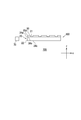
- FIG. 1 is a schematic diagram showing a light guide plate 100 according to an embodiment of the present invention.
- FIG. 1A is a top view of the light guide plate 100.
- FIG. 1B is a cross-sectional view taken along line 1a-1a ′ in FIG.
- the light guide plate 100 includes a light guide member 20 and a diffusion member 30.
- the light guide member 20 and the diffusing member 30 each have two main surfaces.
- the light guide member 20 has a main surface 24a and a main surface 24b.
- the diffusing member 30 has a main surface 30a and a main surface 30b.
- the diffusing member 30 has a plurality of recesses 31 on the main surface 30a of the diffusing member 30 opposite to the main surface 30b adjacent to the light guide member 20.
- Both the main surface 24a and the main surface 24b of the light guide member 20 are substantially flat, and the thickness of the light guide member 20 is substantially constant. Typically, the areas of the main surface 24a and the main surface 24b of the light guide member 20 are equal to each other.
- the light guide member 20 is made of an acrylic resin such as PPMA (polymethyl methacrylate resin).
- a light source (not shown) is typically provided around the light guide member.
- the light incident surface 22 of the light guide member 20 faces the light source, and light from the light source enters the light guide member 20 from the light incident surface 22 of the light guide member 20 as indicated by an arrow Li in FIG. It propagates in the propagation direction P in the direction (x direction) along the main surface 24a and the main surface 24b.
- Light is emitted from the main surface 24a side of the light guide member 20 in the vertical direction (z direction: arrow Lo in FIG. 1) with respect to the main surface 24a and the main surface 24b in the process of propagating through the light guide member 20 in the propagation direction P. Is done.
- the main surface 24a and the main surface 24b may be referred to as a first main surface 24a and a second main surface 24b, respectively.
- the diffusing member 30 is provided on at least one of the first main surface 24 a and the second main surface 24 b of the light guide member 20.
- the diffusion member 30 is provided on the main surface 24 a of the light guide member 20.
- the diffusion member 30 may be formed from the same material as the light guide member 20 or may be formed from a different material. When formed from a different material, the refractive index changes at the interface between the main surface 24 a of the light guide member 20 and the diffusion member 30.
- the diffusion member 30 is made of, for example, an acrylic resin or a polyimide resin.
- the diffusing member 30 may contain beads.
- the beads are made of amorphous silica or acrylic, and the average particle size is about 1 ⁇ m.
- the light incident on the concave surface of the concave portion 31 of the diffusing member 30 diffuses in the concave surface of the concave portion 31 of the diffusing member 30.
- the light incident on the concave surface of the concave portion 31 of the diffusing member 30 may be light that has entered the diffusing member 30 and reached the concave surface in addition to the light that has reflected the light guide member 20 and reached the concave surface.
- the recesses 31 are arranged along the propagation direction P. Specifically, when the main surface 24 a of the light guide member 20 is viewed from the normal direction, the centers of the recesses 31 are arranged substantially linearly along the propagation direction P.
- the length (width) along the x direction and the length (width) along the y direction of the recess 31 are 20 ⁇ m to 70 ⁇ m.
- the thickness (length in the z direction) of the recess 31 is, for example, 5 ⁇ m.
- a fine recess 31 can be suitably formed by gravure offset printing.
- the light guide plate 100 diffuses light from the plurality of recesses 31 of the diffusion member 30. Therefore, since the part which diffuses light does not protrude, the part which diffuses light is not damaged. As a result, the possibility that the uniformity of light is impaired can be eliminated.
- FIG. 2 is a schematic view showing a light guide plate 200 according to another embodiment of the present invention.
- the light guide plate 200 includes a light guide member 20 and a diffusion member 40.
- the diffusion member 40 is formed of a plurality of layers including a first layer 40a, a second layer 40b, and a third layer 40c.
- the light guide plate 200 has the same configuration as that of the light guide plate 100 described with reference to FIG. 1 except that the diffusing member 40 is formed of a plurality of layers.
- the second layer 40b is laminated on the first layer 40a
- the third layer 40c is laminated on the second layer 40b.
- Each of the first layer 40a, the second layer 40b, and the third layer 40c has a plurality of openings, the plurality of openings of the first layer 40a, the plurality of openings of the second layer 40b, and the third.
- the plurality of recesses 41 are formed by aligning the plurality of openings of the layer 40c with each other.
- the materials for forming the first layer, the second layer, and the third layer may be the same, or any of them may be different.
- an acrylic resin such as PPMA (polymethyl methacrylate resin) which is the same material as the light guide member 20 is used as the material of the first layer 40a.
- Acrylic ink mixed with glass frit, bubbles, etc. is used as the material of the second layer 40b.
- a material having a reflectance and a refractive angle different from those of the light guide member 20 is used.
- acrylic ink in which glass frit, bubbles, etc. are mixed in the material of the diffusing member 40, the incident light is likely to be irregularly reflected, and the light can be diffused.
- materials with different reflectivities and refraction angles as the material of the diffusing member 40, the reflection efficiency is increased.
- the diffusion member 40 of the light guide plate 200 is formed of a plurality of layers. Therefore, the diffusing member can be formed from different materials. As a result, the degree of freedom in selecting the combination of materials for the diffusion member is improved.
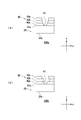
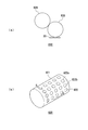
- FIG. 3 is a schematic diagram showing light guide plates 300a and 300b according to still another embodiment of the present invention.
- 3A shows a light guide plate 300a in which the concave surface of the concave portion of the diffusing member 40 is not concave and convex, and FIG.
- the light guide plate 300a has the same configuration as that of the light guide plate 200 described with reference to FIG.
- the light guide plate 300b has the same configuration as the light guide plate 200 described with reference to FIG. 2 except that the concave surface of the concave portion of the diffusing member 40 has a concave and convex shape, and thus description of overlapping portions is omitted.
- the light guide plate 300 b includes a light guide member 20 and a diffusion member 40.
- the concave surface of the concave portion 41 of the diffusing member 40 has an uneven shape.
- the second layer 40b is laminated so as to be shifted from the first layer 40a and the third layer 40c. Since the concave surface of the concave portion 41 of the diffusing member 40 has an uneven shape, light can be diffusely reflected. The larger the uneven width of the uneven shape, the more the light can be diffusely reflected. Therefore, it is preferable that the uneven width of the uneven shape is large. However, the light outlet must not be closed. For example, when the diameter of the opening of the recess is 20 ⁇ m, the uneven width of the uneven shape is 0 ⁇ m to 10 ⁇ m. For example, when the diameter of the opening of the recess is 70 ⁇ m, the uneven width of the uneven shape is 0 ⁇ m to 35 ⁇ m.
- the concavo-convex shape is formed on the bottom surface of the concave surface of the recess 41.
- the thickness of the unevenness on the bottom surface is, for example, 0.5 nm to 10 ⁇ m.
- the thickness is 2 ⁇ m.
- the concave surface of the concave portion 41 of the diffusing member 40 of the light guide plate 300b has an uneven shape. Therefore, light can be diffusely reflected. As a result, light can be diffused and the diffusion efficiency of the light guide plate can be improved.
- FIG. 4 is a schematic view showing a light guide plate 400 according to still another embodiment of the present invention.
- 4A is a top view of the light guide plate 400
- FIG. 4B is a cross-sectional view of the light guide plate 400 taken along line 50a-50a ′.
- the light guide plate 400 includes a light guide member 20 and a diffusion member 30. Of the two main surfaces of the diffusing member 30, the main surface 30 a of the diffusing member 30 opposite to the main surface 30 b adjacent to the light guide member 20 has a plurality of recesses 31.
- the light guide plate 400 has the same configuration as that of the light guide plate 100 described with reference to FIG. 1 except that the size of the concave portion 31 differs depending on the distance from the light incident surface 22, and therefore the overlapping portion will be described. Is omitted.
- the size of the recess 31 varies depending on the distance from the light incident surface 22.
- the concave portions 31 are arranged so that the larger the distance from the light incident surface 22, the larger the size when the main surface 24 a is viewed from the normal direction.
- the light incident from the light incident surface is attenuated by reflection in the light guide plate as the propagation distance becomes longer, so that the intensity of light diffused from the light guide plate decreases as the distance from the light incident surface increases.
- the recesses 31 are arranged so that the size increases as the distance from the light incident surface 22 increases, and the reflection efficiency increases as the distance from the light incident surface 22 increases. As the distance from the light incident surface 22 increases, the amount of light reaching the recess 31 decreases, but the intensity of light from the light guide plate 400 can be made uniform.
- each of the recess 31a and the recess 31b has a circular shape.
- the recess 31a and the recess 31b may be referred to as a first recess 31a and a second recess 31b, respectively.
- the recesses 31 a and the recesses 31 b are arranged so that the centers of the recesses 31 a and the recesses 31 b are along the propagation direction P of the light incident from the light incident surface 22.
- the size of the second recess 31b is larger than the size of the first recess 31a.
- the light guide plate 400 of the present embodiment is configured to increase in size as the distance from the light incident surface 22 increases even when the vicinity of each recess 31 is viewed locally as well as the entire main surface 24a.
- the intensity of light from the light guide plate 400 can be made more uniform.
- the diffusion efficiency is improved by providing the concave portion 31 so as to increase in size as the distance from the light incident surface 22 increases.
- FIG. 5 is a schematic view showing a light guide plate 500 according to still another embodiment of the present invention.
- 5A is a top view of the light guide plate 500
- FIG. 5B is a cross-sectional view of the light guide plate 500 taken along line 50b-50b '.
- the light guide plate 500 includes a light guide member 20 and a diffusion member 30. Of the two main surfaces of the diffusing member 30, the main surface 30 a and the main surface 30 b, a plurality of recesses 31 are formed on the main surface 30 a of the diffusing member 30 opposite to the main surface 30 b adjacent to the light guide member 20. Have.
- the light guide plate 500 has the same configuration as the light guide plate 400 described with reference to FIG. 4 except that the recess (length in the z direction) of the recess 31 differs depending on the distance from the light incident surface 22. Description of overlapping parts is omitted.
- the recess (length in the z direction) of the recess 31 varies depending on the distance from the light incident surface 22.
- the recesses 31 are arranged such that the recesses (the length in the z direction) increase as the distance from the light incident surface 22 increases.
- the thickness is 1 ⁇ m, 2 ⁇ m, 3 ⁇ m, and 4 ⁇ m in order from the concave portion 31 close to the light incident surface 22.
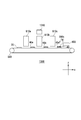
- FIG. 6 is a schematic view of a light guide plate 600 according to another embodiment of the present invention.
- the light guide plate 600 includes the light guide member 20, the diffusion member 30, and the reflective film 60. Since the light guide plate 600 has the same configuration as that of the light guide plate 100 described with reference to FIG. 1 except that the reflective film 60 is provided, the description of the overlapping portions is omitted.
- the light guide plate 600 has a main surface 24b of the light guide member 20 opposite to the main surface 24a adjacent to the diffusing member 30 out of the two main surfaces 24a and 24b that are two main surfaces of the light guide member 20.
- a reflective film 60 is provided. That is, in the light guide plate 600, the reflective film is provided on the main surface 24b opposite to the light emission direction Lo.
- the reflective film 60 reflects the light that has reached the main surface 24b.
- the reflective film is, for example, a white sheet formed by adding titanium oxide to an aromatic polyester resin.
- the thickness of the reflective film 60 is, for example, 15 ⁇ m to 25 ⁇ m, but may be about 200 ⁇ m.
- the reflection film has to be formed on the main surface side on which the dot pattern is formed.
- the dot pattern protrudes, it is necessary to provide an air layer between the dot pattern and the reflective film.
- a reflective film may be formed on the main surface 24b. Therefore, since the reflective film 60 can be provided on a flat surface, it is not necessary to provide an air layer.
- the reflective film 60 is provided on the main surface opposite to the diffusing member, there is no possibility of damaging the diffusing member due to the reflective film 60 coming into contact with the diffusing member 30. Further, since there is no air layer, there is no loss of light due to the air layer, and the luminous efficiency can be improved.
- the reflective film 60 is provided on a flat surface, and the reflective film 60 can be provided by printing.
- FIG. 7 is a schematic diagram showing a light source device 700 according to an embodiment of the present invention.
- the light source device 700 includes a light guide plate 100 and a light source 70. Since the light guide plate 100 has the same configuration as that of the light guide plate 100 described with reference to FIG.
- the light source 70 is provided to face the light incident surface 22 of the light guide plate 100.
- the light source 70 emits light incident on the light guide member 20.
- the light source device 700 can be used as a lighting fixture.
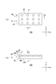
- FIG. 8 is a schematic diagram showing a light guide plate manufacturing apparatus 800 according to an embodiment of the present invention.
- FIG. 9A is a schematic diagram illustrating the printing unit 810.
- FIG. 9B is a schematic diagram showing the plate roll 820.
- the light guide plate manufacturing apparatus 800 manufactures the light guide plate 100 described with reference to FIG. In the following description, the light guide plate manufacturing apparatus 800 may be simply referred to as the manufacturing apparatus 800.
- the manufacturing apparatus 800 includes a printing unit 810.
- the printing unit 810 includes a plate roll 820 and a transfer roll 830.
- the printing unit 810 prints the ink that forms the diffusion member 30 on the light guide member 20.
- the plate roll 820 and the transfer roll 830 can rotate. Here, the diameters of the plate roll 820 and the transfer roll 830 are substantially equal.
- the surface of the plate roll 820 is treated with metal plating.
- a concave groove is formed in the plate roll 820 in a predetermined pattern. This pattern corresponds to a line, a figure, a pattern, or the like printed on the light guide member 20.
- the transfer roll 830 includes a metal tube and a blanket, and the blanket is provided so as to cover the outer peripheral surface of the metal tube.
- the blanket is formed from rubber.
- the blanket is formed from silicone rubber.
- the metal tube is made of, for example, iron or aluminum.
- the surface of the plate roll 820 is provided with an ink filling portion 821 and a plurality of convex portions 822 having a shape corresponding to the plurality of concave portions 31 of the diffusion member 30 (FIG. 9B).
- attention is focused on two convex portions 822a and 822b adjacent to each other.
- the convex part 822a and the convex part 822b may be referred to as a first convex part 822a and a second convex part 822b, respectively.
- the first convex portion 822a and the second convex portion 822b are provided along the direction R.
- the direction R of the convex portions 822a and 822b arranged in a straight line is provided along the rotation direction of the plate roll 820, but the present invention is not limited to this.
- the direction R may be along the direction of the generatrix of the cylindrical plate roll 820.
- the light guide member 20 is preferably transported to the positions of the plate roll 820 and the transfer roll 830.
- the manufacturing apparatus 800 further includes a transport unit 840 that transports the light guide member 20.
- the conveyance unit 840 is a conveyor, and the conveyance unit 840 conveys the light guide member 20 to the fixed plate roll 820 and the transfer roll 830.
- the manufacturing apparatus 800 may further include a drying device 850 that dries the ink.
- FIG. 10 is a schematic view for explaining the method of manufacturing the light guide plate of the present invention.
- a light guide member 20 having a light incident surface 22, a main surface 24a, and a main surface 24b is prepared.
- ink for forming the diffusion member 30 is printed on the main surface 24a of the light guide member 20.
- the diffusing member 30 has a plurality of recesses 31 on the main surface 30a of the diffusing member 30 opposite to the main surface 30b adjacent to the light guide member 20.
- the ink forming the diffusion member 30 is printed on the main surface 24a of the light guide member 20, but the ink forming the diffusion member 30 may be printed on the main surface 24b of the light guide member 20, Or you may print on both the main surface 24a and the main surface 24b.
- the light guide member 20 is formed of an acrylic resin such as PPMA (polymethyl methacrylate resin).
- PPMA polymethyl methacrylate resin
- the plate roll 820 is made of metal, and the blanket of the transfer roll 830 is made of resin.
- the light guide plate 100 by gravure offset printing.
- the gravure offset printing can reduce the amount of material used for the diffusion member 30 and can form the diffusion member 30 simply and at high speed.
- a plurality of fine concave portions 31 can be realized by gravure offset printing, and the diffusion member 30 can be formed of a material different from that of the light guide member 20.
- the diffusing member 30 may be formed from substantially the same material as the light guide member 20.
- FIG. 11 is a schematic view showing a light guide plate manufacturing apparatus 1100 according to another embodiment of the present invention.
- the light guide plate manufacturing apparatus 1100 manufactures the light guide plate 200 described with reference to FIG.
- the light guide plate manufacturing apparatus 1100 includes a first printing unit 810a, a second printing unit 810b, and a third printing unit 810c.
- the light guide plate manufacturing apparatus 1100 has the same configuration as that of the light guide plate manufacturing apparatus 800 described with reference to FIG. 8 except that a plurality of printing units are provided, and thus description of overlapping portions is omitted.
- the light guide plate manufacturing apparatus 1100 may be simply referred to as the manufacturing apparatus 1100.
- the manufacturing apparatus 1100 includes a plurality of printing units.
- the first printing unit 810a includes a first transfer roll and a first plate roll corresponding to the shape of the first layer 40a of the diffusion member 40.
- the second printing unit 810b includes a second transfer roll and a second plate roll corresponding to the shape of the second layer 40b of the diffusion member 40.
- the third printing unit 810c includes a third transfer roll and a third plate roll corresponding to the shape of the third layer 40c of the diffusion member 40.
- Each of the first plate roll, the second plate roll, and the third plate roll is formed with a plurality of convex portions having shapes corresponding to the plurality of concave portions of the ink filling portion and the diffusion member.
- the method for manufacturing the light guide plate 200 includes a first step, a second step, and a third step.
- the light guide member 20 is placed on the transport unit 840, and the transport unit 840 transports the light guide member 20.
- the first printing unit 810 a supplies ink that forms the first layer 40 a of the diffusing member 40 to the light guide member 20. It prints so that it may laminate
- the second printing unit 810b uses the ink that forms the second layer 40b of the diffusion member 40. Printing is performed so as to be stacked on the first layer 40a (second step). Subsequently, after the second printing unit 810b performs printing, when the light guide member 20 reaches below the third printing unit 810c, the third printing unit 810c uses the ink that forms the third layer 40c of the diffusing member 40. Printing is performed so as to be stacked on the second layer 40b (third step).
- the light guide plate 200 can be manufactured from the light guide member 20 through the first step, the second step, and the third step described above.
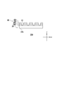
- FIG. 12A is a schematic diagram showing a light guide plate manufacturing apparatus 1200 according to still another embodiment of the present invention
- FIG. 12B is a light guide plate manufacturing apparatus 1200 according to another embodiment of the present invention.
- FIG. The light guide plate manufacturing apparatus 1200 manufactures the light guide plate 300b described with reference to FIG.
- the light guide plate manufacturing apparatus 1200 will be described with reference to FIG. 11 except that the second printing unit 810b is provided so that the second layer 40b of the diffusing member 40 is printed out of alignment with the first layer 40a. Since it has the same configuration as the light guide plate manufacturing apparatus 1100, the description of the overlapping parts is omitted.
- the light guide plate manufacturing apparatus 1200 may be simply referred to as a manufacturing apparatus 1200.
- the manufacturing apparatus 1200 includes a plurality of printing units.
- the light guide plate manufacturing apparatus 1200 includes a first printing unit 810a, a second printing unit 810b, and a third printing unit 810c.
- a center line 1210 indicates a center line passing through the centers of the first printing unit 810a and the third printing unit 810c.
- a center line 1220 indicates a center line passing through the center of the second printing unit 810b.
- the second printing unit 810b is provided so as to be shifted in the y direction with respect to the center line 1210.
- the second printing unit 810b By disposing the second printing unit 810b in the y direction with respect to the center line 1210, the second layer 40b of the diffusing member 40 is shifted in the y direction with respect to the first layer 40a and the third layer 40c. Printed. As a result, the light guide plate 300b in which the concave surface of the concave portion 41 of the diffusing member has an uneven shape can be manufactured.
- FIG. 13 is a schematic diagram showing a light guide plate manufacturing apparatus 1300 according to still another embodiment of the present invention.
- the light guide plate manufacturing apparatus 1300 manufactures the light guide plate 300b described with reference to FIG.
- the light guide plate manufacturing apparatus 1300 has the same configuration as that of the light guide plate manufacturing apparatus 1100 described with reference to FIG. 11 except that it further includes a timing adjustment unit 1310, and thus description of overlapping portions is omitted.
- the light guide plate manufacturing apparatus 1300 may be simply referred to as a manufacturing apparatus 1300.
- the manufacturing apparatus 1300 further includes timing adjustment means 1310.
- the timing adjusting unit 1310 adjusts the printing timing of the second layer 40b so that the second layer 40b of the diffusing member 40 is printed out of alignment with the first layer 40a. For example, when the rotation speeds of the transfer roll of the first printing unit 810a and the transfer roll of the second printing unit 810b are the same, the second layer 40b of the diffusing member 40 is printed so as to be shifted from the first layer 40a. The printing start position of the transfer roll of the second printing unit 810b is shifted from the printing start position of the transfer roll of the first printing unit 810a.
- the rotation speed of the transfer roll of the second printing unit 810b is adjusted so that the second layer 40b of the diffusing member 40 is printed out of alignment with the first layer 40a.
- the position of the first layer 40a of the diffusion member 40 printed on the light guide member 20 is measured, and the rotation speed of the transfer roll is determined based on the measured position of the first layer 40a. Adjust.
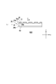
- FIG. 14 is a development view of a plate roll of a light guide plate manufacturing apparatus according to still another embodiment of the present invention.
- the upper view of FIG. 14 is a development view of the first plate roll 1400a
- the lower view of FIG. 14 is a development view of the second plate roll 1400b.
- the first plate roll 1400a has a plurality of convex portions 1410a and an ink filling portion 1420a.
- the second plate roll 1400b has a plurality of convex portions 1410b and an ink filling portion 1420b.
- the center line 1430a indicates the center line of the protrusion 1410a
- the center line 1430b indicates the center line of the protrusion 1410b.
- the center line 1430b is shifted in the x direction with respect to the center line 1430a.
- the plurality of convex portions 1410b of the second plate roll 1400b are shifted in a predetermined direction with respect to the plurality of convex portions 1410a of the first plate roll 1400a, and as a result, the first layer 40a and the second layer 40b are separated and printed. Therefore, the light guide plate 300b described with reference to FIG. 3B can be manufactured.
- the second plate roll 1400b is shifted in the x direction with respect to the first plate roll 1400a
- the second plate roll 1400b may be shifted in the y direction with respect to the first plate roll 1400a.
- FIG. 15 is a development view of a plate roll 1500 of a light guide plate manufacturing apparatus according to still another embodiment of the present invention.
- the plate roll 1500 is provided with a plurality of convex portions 1510 including a first convex portion 1510a and a second convex portion 1510b, and an ink filling portion 1520.
- the 1st convex part 1510a and the 2nd convex part 1510b are provided along the x direction, and the magnitude
- FIG. 16 is a schematic view showing a light guide plate manufacturing apparatus 1600 according to still another embodiment of the present invention.
- the light guide plate manufacturing apparatus 1600 manufactures the light guide plate 600 described with reference to FIG.
- the light guide plate manufacturing apparatus 1600 includes a printing unit 1610 and a reflective film printing unit 1620.
- the printing unit 1610 includes a plate roll 1611 and a transfer roll 1612.
- the reflective film printing unit 1620 includes a plate roll 1621 and a transfer roll 1622.
- the reflective film printing unit 1620 is provided at a position facing the printing unit 1610.
- the printing unit 1610 prints the ink that forms the diffusion member 30 on the main surface 24 a of the light guide member 20.
- the reflective film printing unit 1620 prints ink that forms the reflective film 60 on the main surface 24 b of the light guide member 20.
- the light guide plate manufacturing apparatus 1600 may further include a transport unit 1630 and a transport unit 1631 that transport the light guide member 20.
- the conveyance unit 1630 and the conveyance unit 1631 are conveyors.
- the transport unit 1630 and the transport unit 1631 transport the light guide member 20.
- the conveyance unit 1631 is provided at a position facing the conveyance unit 1630 via the reflective film printing unit 1620.
- the light guide plate manufacturing apparatus 1600 may further include a drying device 850 that dries the ink forming the diffusing member 30 and the ink forming the reflective film 60. If the ink is cured by UV, a UV lamp may be provided instead of the drying device 850.
- the light guide member 20 is conveyed so that the main surface 24a and the main surface 24b of the light guide member 20 are directed in the vertical direction (z direction).
- the light guide member 20 is conveyed so that the main surface 24b is oriented in the horizontal direction (y direction), and the light guide member 20 is sandwiched from the horizontal direction (y direction) between the printing unit 1610 and the reflective film printing unit 1620, thereby guiding the light guide plate. 600 may be manufactured.
- the embodiment of the light guide plate 200 in which the diffusing member 40 is formed of a plurality of layers including the first layer 40a and the second layer 40b, and each of the first layer 40a and the second layer 40b is the same.
- An embodiment of the light guide plate 200 formed of a material, an embodiment of the light guide plate 200 formed of a different material in each of the first layer 40a and the second layer 40b, and the concave surfaces of the plurality of concave portions 41 are uneven.
- the embodiment of the light guide plate 300b, the embodiment of the light guide plate 400 and the light guide plate 500 in which the size of the second recess 31b is larger than the size of the first recess 31a, and the embodiment of the light guide plate 600 including the reflective film 60 have been described.
- an embodiment in which constituent elements of at least two of the light guide plate embodiments are combined as will be apparent to those skilled in the art is also an embodiment of the present invention.
- the light guide plate of the present invention is suitably used for a liquid crystal display device or a lighting device.
- Light guide member 22 Light incident surface 24a, 24b Main surface 30 of light guide member Diffusion member 30a, 30b Main surface 31 of diffusion member Recess 31a First recess 31b Second recess 40 Diffusion member 40a First layer 40b Second layer 40c Third layer 41 Recess 60 Reflective film 70 Light source 100 Light guide plate 200 Light guide plate 300a Light guide plate 300b Light guide plate 400 Light guide plate 500 Light guide plate 600 Light guide plate 700 Light guide plate 800 Light guide plate manufacturing apparatus 810 Printing unit 810a First printing unit 810b Second Printing section 810c Third printing section 820 Plate roll 821 Ink filling section 822 Convex section 822a First convex section 822b Second convex section 830 Transfer roll 840 Conveying section 850 Drying apparatus 1100 Light guide plate manufacturing apparatus 1200 Light guide plate manufacturing apparatus 1300 Light guide plate manufacturing apparatus 1300 Equipment 1310 Thailand 1400a first plate roll 1400b second plate roll 1410a, 1410b convex portion 1420a, 1420b ink filling portion 1430a
Landscapes
- Physics & Mathematics (AREA)
- Optics & Photonics (AREA)
- General Physics & Mathematics (AREA)
- Engineering & Computer Science (AREA)
- Manufacturing & Machinery (AREA)
- Planar Illumination Modules (AREA)
- General Engineering & Computer Science (AREA)
- Microelectronics & Electronic Packaging (AREA)
- Light Guides In General And Applications Therefor (AREA)
Description
図1を参照して本発明による導光板100の実施形態を説明する。図1は、本発明の実施形態に係る導光板100を示す模式図である。図1(a)は導光板100の上面図である。図1(b)は図1(a)の1a-1a’線に沿った断面図である。
図2は、本発明の他の実施形態に係る導光板200を示す模式図である。導光板200は、導光部材20と、拡散部材40とを備える。拡散部材40は、第1層40aと第2層40bと第3層40cとを含む複数の層から形成されている。導光板200は、拡散部材40が複数の層から形成される点を除いて図1を参照して説明した導光板100と同様な構成を有するため、重複部分については説明を省略する。
図3は、本発明の更に他の実施形態に係る導光板300aおよび300bを示す模式図である。図3(a)は拡散部材40の凹部の凹面が凹凸形状でない導光板300aを示し、図3(b)は拡散部材40の凹部の凹面が凹凸形状である導光板300bを示す。導光板300aは、図2を参照して説明した導光板200と同様な構成を有するため、重複部分については説明を省略する。導光板300bは、拡散部材40の凹部の凹面が凹凸形状である点を除いて図2を参照して説明した導光板200と同様な構成を有するため、重複部分については説明を省略する。
図4は、本発明の更に他の実施形態に係る導光板400を示す模式図である。図4(a)は導光板400の上面図であり、図4(b)は導光板400の50a-50a’線に沿った断面図である。
図6は、本発明の他の実施形態に係る導光板600の模式図である。導光板600は、導光部材20と、拡散部材30と、反射フィルム60とを備える。導光板600は、反射フィルム60を備える点を除いて図1を参照して説明した導光板100と同様な構成を有するため、重複部分については説明を省略する。
図7は、本発明の実施形態に係る光源装置700を示す模式図である。光源装置700は、導光板100と光源70とを備える。導光板100は、図1を参照して説明した導光板100と同様な構成を有するため、重複部分については説明を省略する。光源70は導光板100の光入射面22に対向するように設けられる。光源70は導光部材20に対して入射する光を発する。照明器具として、光源装置700を使用することができる。
以下、図8および図9を参照して本発明による導光板製造装置800の実施形態を説明する。図8は、本発明の実施形態に係る導光板製造装置800を示す模式図である。図9(a)は、印刷部810を示す模式図である。図9(b)は、版ロール820を示す模式図である。導光板製造装置800は、図1を参照して説明した導光板100を製造する。以下の説明において、導光板製造装置800を単に製造装置800と記載することがある。
図10は、本発明の導光板の製造方法を説明するための模式図である。以下、図8~図10を参照して、導光板100の製造方法の一例を説明する。はじめに、図10(a)に示すように、光入射面22、主面24a、主面24bを有する導光部材20を用意する。
図11は、本発明の他の実施形態に係る導光板製造装置1100を示す模式図である。導光板製造装置1100は、図2を参照して説明した導光板200を製造する。導光板製造装置1100は第1印刷部810aと第2印刷部810bと第3印刷部810cとを備える。導光板製造装置1100は、印刷部を複数備える点を除いて図8を参照して説明した導光板製造装置800と同様な構成を有するため、重複部分については説明を省略する。以下の説明において、導光板製造装置1100を単に製造装置1100と記載することがある。
以下、図11を参照して、導光板200の製造方法の一例を説明する。導光板200の製造方法は、第1工程と第2工程と第3工程とを包含する。最初に、搬送部840の上に導光部材20が載置され、搬送部840は導光部材20を搬送する。続いて、搬送部840によって搬送された導光部材20が第1印刷部810aの下に到達すると、第1印刷部810aは拡散部材40の第1層40aを形成するインクを導光部材20の上に積層するように印刷する(第1工程)。続いて、第1印刷部810aが印刷を行った後に、導光部材20が第2印刷部810bの下に到達すると、第2印刷部810bは拡散部材40の第2層40bを形成するインクを第1層40aの上に積層するように印刷する(第2工程)。続いて、第2印刷部810bが印刷を行った後に、導光部材20が第3印刷部810cの下に到達すると、第3印刷部810cは拡散部材40の第3層40cを形成するインクを第2層40bの上に積層するように印刷する(第3工程)。上述した第1工程、第2工程、第3工程を経て、導光部材20から導光板200を製造することができる。
図12(a)は、本発明の更に他の実施形態に係る導光板製造装置1200を示す模式図であり、図12(b)は、本発明の他の実施形態に係る導光板製造装置1200の模式的な上面図である。導光板製造装置1200は、図3(b)を参照して説明した導光板300bを製造する。導光板製造装置1200は、拡散部材40の第2層40bが第1層40aに対してずれて印刷されるように第2印刷部810bを設けた点を除いて、図11を参照して説明した導光板製造装置1100と同様な構成を有するため、重複部分については説明を省略する。以下の説明において、導光板製造装置1200を単に製造装置1200と記載することがある。
図13は、本発明の更に他の実施形態に係る導光板製造装置1300を示す模式図である。導光板製造装置1300は、図3(b)を参照して説明した導光板300bを製造する。導光板製造装置1300は、タイミング調整手段1310を更に備える点を除いて図11を参照して説明した導光板製造装置1100と同様な構成を有するため、重複部分については説明を省略する。以下の説明において、導光板製造装置1300を単に製造装置1300と記載することがある。
図14は、本発明の更に他の実施形態に係る導光板製造装置の版ロールの展開図である。図14の上図は第1版ロール1400aの展開図であり、図14の下図は第2版ロール1400bの展開図である。
図15は、本発明の更に他の実施形態に係る導光板製造装置の版ロール1500の展開図である。
図16は、本発明の更に他の実施形態に係る導光板製造装置1600を示す模式図である。導光板製造装置1600は、図6を参照して説明した導光板600を製造する。導光板製造装置1600は、印刷部1610と反射フィルム印刷部1620とを備える。印刷部1610は版ロール1611と転写ロール1612とを備える。反射フィルム印刷部1620は版ロール1621と転写ロール1622とを備える。反射フィルム印刷部1620は、印刷部1610と対向する位置に設けられる。印刷部1610は、導光部材20の主面24aに、拡散部材30を形成するインクを印刷する。反射フィルム印刷部1620は、導光部材20の主面24bに、反射フィルム60を形成するインクを印刷する。導光板製造装置1600は、導光部材20を搬送する搬送部1630と搬送部1631とをさらに備えてもよい。搬送部1630と搬送部1631とはコンベアである。搬送部1630と搬送部1631とは、導光部材20を搬送する。搬送部1631は、反射フィルム印刷部1620を介して搬送部1630と対向する位置に設けられる。導光板製造装置1600は、拡散部材30を形成するインク及び反射フィルム60を形成するインクを乾燥させる乾燥装置850をさらに備えてもよい。インクがUVによって硬化する場合、乾燥装置850の代わりにUVランプを備えてもよい。
22 光入射面
24a、24b 導光部材の主面
30 拡散部材
30a、30b 拡散部材の主面
31 凹部
31a 第1凹部
31b 第2凹部
40 拡散部材
40a 第1層
40b 第2層
40c 第3層
41 凹部
60 反射フィルム
70 光源
100 導光板
200 導光板
300a 導光板
300b 導光板
400 導光板
500 導光板
600 導光板
700 導光板
800 導光板製造装置
810 印刷部
810a 第1印刷部
810b 第2印刷部
810c 第3印刷部
820 版ロール
821 インク充填部
822 凸部
822a 第1凸部
822b 第2凸部
830 転写ロール
840 搬送部
850 乾燥装置
1100 導光板製造装置
1200 導光板製造装置
1300 導光板製造装置
1310 タイミング調整手段
1400a 第1版ロール
1400b 第2版ロール
1410a、1410b 凸部
1420a、1420b インク充填部
1430a、1430b 中心線
1500 版ロール
1510 凸部
1510a 第1凸部
1510b 第2凸部
1520 インク充填部
1600 導光板製造装置
1610 印刷部
1611 版ロール
1612 転写ロール
1620 反射フィルム印刷部
1621 版ロール
1622 転写ロール
1630、1631 搬送部
Claims (17)
- 第1主面および第2主面を有する導光部材と、
前記導光部材の前記第1主面および前記第2主面のうちの少なくとも一方に隣接して設けられた拡散部材と
を備える導光板であって、
前記拡散部材が有する2つの主面のうち、前記導光部材に隣接する主面とは反対側の前記拡散部材の主面に複数の凹部を有し、前記導光部材に入射した光を前記複数の凹部で拡散させる、導光板。 - 前記複数の凹部の凹面は凹凸形状である、請求項1に記載の導光板。
- 前記複数の凹部は、第1凹部および第2凹部を含み、
前記導光部材の前記第1主面を法線方向から見た場合、
光の入射面と前記第2凹部との間の距離は前記光の入射面と前記第1凹部との間の距離よりも大きく、前記第2凹部の大きさは前記第1凹部の大きさよりも大きい、請求項1又は請求項2に記載の導光板。 - 前記導光部材が有する2つの主面のうち、前記拡散部材に隣接する主面とは反対側の前記導光部材の主面に、前記入射した光を反射する反射フィルムを備える、請求項1から請求項3のうちの1項に記載の導光板。
- 前記拡散部材は、第1層と第2層とを含む複数の層から形成される、請求項1から請求項4のうちの1項に記載の導光板。
- 前記第1層と前記第2層との各々は、同じ材料から形成される、請求項5に記載の導光板。
- 前記第1層と前記第2層との各々は、異なる材料から形成される、請求項6に記載の導光板。
- 請求項1から請求項7のうちの1項に記載の導光板と、
前記導光部材に対して入射する光を発する光源と
を備える、光源装置。 - 拡散部材を形成するインクを導光部材に印刷する印刷部を備えた導光板製造装置であって、
前記印刷部は、版ロールと転写ロールとを備え、
前記版ロールには、インク充填部と、前記拡散部材が有する複数の凹部に対応する形状である複数の凸部とが形成されており、
前記版ロールは、前記インク充填部に充填された前記インクを前記転写ロールに転写し、
前記転写ロールは、前記インクを前記導光部材に印刷する、導光板製造装置。 - 前記拡散部材は、第1層と第2層とを含む複数の層を有し、
前記導光板製造装置は、
前記拡散部材の前記第1層を形成するインクを印刷する第1印刷部と
前記拡散部材の前記第2層を形成するインクを印刷する第2印刷部と
を備え、
前記第1印刷部は、第1転写ロールと前記第1層の形状に対応する第1版ロールとを有し、
前記第2印刷部は、第2転写ロールと前記第2層の形状に対応する第2版ロールとを有する、請求項9に記載の導光板製造装置。 - 前記第2層が前記第1層に対してずれて印刷されるように前記第2印刷部を設けた、請求項10に記載の導光板製造装置。
- 前記第2層が前記第1層に対してずれて印刷されるように前記第2層の印刷タイミングを調整するタイミング調整手段を設ける、請求項10に記載の導光板製造装置。
- 前記第1版ロールと前記第2版ロールとにはそれぞれ前記拡散部材が有する複数の凹部に対応する形状である複数の凸部が形成されており、前記第2版ロールの前記複数の凸部は前記第1版ロールの前記複数の凸部に対して所定方向にずれている、請求項10に記載の導光板製造装置。
- 前記版ロールには、第1凸部および第2凸部を含む複数の凸部が設けられており、
前記第1凸部および前記第2凸部は所定の方向に沿って設けられており、
前記第2凸部の大きさは前記第1凸部の大きさよりも大きい、請求項9から請求項13のうちの1項に記載の導光板製造装置。 - 反射フィルムを形成するインクを印刷する反射フィルム印刷部を更に備え、 前記反射フィルム印刷部は、前記印刷部と対向して設けられる、請求項9から請求項14のうちの1項に記載の導光板製造装置。
- 第1主面および第2主面を有する導光部材を用意する用意工程と、
前記導光部材の前記第1主面および前記第2主面のうちの少なくとも一方に隣接するように、拡散部材を形成するインクを印刷する印刷工程と
を包含する導光板製造方法であって、
前記拡散部材が有する2つの主面のうち、前記導光部材に隣接する主面とは反対側の前記拡散部材の主面に複数の凹部を有し、前記導光部材に入射した光を前記複数の凹部で拡散させる、導光板製造方法。 - 前記拡散部材は、第1層と第2層とを含む複数の層を有し、
前記印刷工程は、
前記拡散部材の前記第1層を形成するインクを印刷する第1工程と、
前記拡散部材の前記第2層を形成するインクを印刷する第2工程と
を包含する、請求項16に記載の導光板製造方法。
Priority Applications (5)
| Application Number | Priority Date | Filing Date | Title |
|---|---|---|---|
| KR1020157003709A KR101794792B1 (ko) | 2012-07-27 | 2013-07-19 | 도광판, 광원 장치, 도광판 제조 장치 및 도광판의 제조 방법 |
| US14/417,380 US9880340B2 (en) | 2012-07-27 | 2013-07-19 | Light guide plate, light source device, light guide plate manufacturing apparatus, and method for manufacturing light guide plate |
| EP13822738.4A EP2878877A4 (en) | 2012-07-27 | 2013-07-19 | LIGHT GUIDE PLATE, ITS MANUFACTURING DEVICE AND ITS MANUFACTURING METHOD, AND LIGHT SOURCE DEVICE |
| CN201380039968.9A CN104508357B (zh) | 2012-07-27 | 2013-07-19 | 导光板、光源装置、导光板制造装置及导光板制造方法 |
| JP2014526896A JP6324311B2 (ja) | 2012-07-27 | 2013-07-19 | 導光板、光源装置、導光板製造装置および導光板の製造方法 |
Applications Claiming Priority (2)
| Application Number | Priority Date | Filing Date | Title |
|---|---|---|---|
| JP2012-166720 | 2012-07-27 | ||
| JP2012166720 | 2012-07-27 |
Publications (1)
| Publication Number | Publication Date |
|---|---|
| WO2014017400A1 true WO2014017400A1 (ja) | 2014-01-30 |
Family
ID=49997213
Family Applications (1)
| Application Number | Title | Priority Date | Filing Date |
|---|---|---|---|
| PCT/JP2013/069653 Ceased WO2014017400A1 (ja) | 2012-07-27 | 2013-07-19 | 導光板、光源装置、導光板製造装置および導光板の製造方法 |
Country Status (7)
| Country | Link |
|---|---|
| US (1) | US9880340B2 (ja) |
| EP (1) | EP2878877A4 (ja) |
| JP (1) | JP6324311B2 (ja) |
| KR (1) | KR101794792B1 (ja) |
| CN (1) | CN104508357B (ja) |
| TW (1) | TWI526722B (ja) |
| WO (1) | WO2014017400A1 (ja) |
Cited By (1)
| Publication number | Priority date | Publication date | Assignee | Title |
|---|---|---|---|---|
| KR20200092195A (ko) * | 2019-01-24 | 2020-08-03 | 엘지이노텍 주식회사 | 조명 장치 |
Families Citing this family (5)
| Publication number | Priority date | Publication date | Assignee | Title |
|---|---|---|---|---|
| JP6791284B2 (ja) * | 2019-02-22 | 2020-11-25 | ダイキン工業株式会社 | ドレンパン、ドレンパンユニット、及び空気調和装置 |
| KR102683664B1 (ko) * | 2019-07-30 | 2024-07-11 | 주식회사 엘지화학 | 확산 및 재귀 반사가 가능한 복합기능시트, 이의 제조방법 및 이를 포함하는 백라이트 유닛 |
| KR20210143501A (ko) | 2020-05-20 | 2021-11-29 | 엘지이노텍 주식회사 | 조명모듈, 조명장치 및 후미등 |
| CN113156567B (zh) * | 2021-02-07 | 2022-09-02 | 捷开通讯(深圳)有限公司 | 导光板和显示装置 |
| EP4647301A1 (en) * | 2024-05-09 | 2025-11-12 | FERRARI S.p.A. | Automotive lighting unit |
Citations (6)
| Publication number | Priority date | Publication date | Assignee | Title |
|---|---|---|---|---|
| JPH08160423A (ja) * | 1994-12-02 | 1996-06-21 | Nissha Printing Co Ltd | 面光源装置及びその製造方法 |
| JPH0955111A (ja) * | 1995-08-15 | 1997-02-25 | Minebea Co Ltd | 面状光源装置に用いる基板の製造方法 |
| JP2007242856A (ja) * | 2006-03-08 | 2007-09-20 | Rohm Co Ltd | チップ型半導体発光素子 |
| JP2009000875A (ja) * | 2007-06-20 | 2009-01-08 | Sony Corp | 印刷装置および印刷方法 |
| JP2010225562A (ja) * | 2009-03-25 | 2010-10-07 | Sharp Corp | 導光体およびバックライトシステム |
| JP2012053273A (ja) | 2010-09-01 | 2012-03-15 | Sumitomo Chemical Co Ltd | 導光板及びこれを用いたエッジライト型面光源装置 |
Family Cites Families (25)
| Publication number | Priority date | Publication date | Assignee | Title |
|---|---|---|---|---|
| JP2869826B2 (ja) * | 1991-08-28 | 1999-03-10 | キヤノン株式会社 | 半導体製造方法 |
| JPH0555103U (ja) | 1991-12-27 | 1993-07-23 | オーツタイヤ株式会社 | 導光板装置 |
| JP3008932B2 (ja) | 1998-07-17 | 2000-02-14 | 日本電気株式会社 | 背面照明装置 |
| JP3271660B2 (ja) | 1999-01-19 | 2002-04-02 | 恵和株式会社 | 光路制御拡散シート及びこれを用いたバックライトユニット |
| US20030214719A1 (en) * | 2002-05-16 | 2003-11-20 | Eastman Kodak Company | Light diffuser containing perimeter light director |
| JP4073250B2 (ja) | 2002-05-21 | 2008-04-09 | シチズン電子株式会社 | バックライトユニット |
| TW200540527A (en) | 2004-02-26 | 2005-12-16 | Takiron Co | Light diffusing sheet, and backlight unit using the light diffusing sheet |
| CN2921887Y (zh) | 2006-04-03 | 2007-07-11 | 中强光电股份有限公司 | 背光模块 |
| JP5298857B2 (ja) * | 2007-01-12 | 2013-09-25 | コニカミノルタ株式会社 | 反射防止フィルムの製造方法 |
| TWI518376B (zh) | 2007-02-21 | 2016-01-21 | 王子控股股份有限公司 | 凹凸圖案形成片及其製造方法 |
| DE102008021721A1 (de) * | 2007-05-08 | 2008-11-27 | Citizen Electronics Co., Ltd., Fujiyoshida-shi | Optisches Bauteil, Hintergrundbeleuchtungseinheit und Anzeigevorrichtung |
| DE112008002087T5 (de) | 2007-08-02 | 2010-06-10 | Daicel Chemical Industries, Ltd., Osaka-shi | Lichtstreuende Folie und damit ausgestattete Vorrichtung |
| CN101363934B (zh) * | 2007-08-10 | 2011-08-31 | 北京京东方光电科技有限公司 | 导光板加工方法和加工设备 |
| CN101910879B (zh) | 2008-01-24 | 2013-10-09 | 木本股份有限公司 | 光扩散性薄片及使用其的背光装置 |
| KR100867919B1 (ko) * | 2008-02-29 | 2008-11-10 | 주식회사 엘엠에스 | 광학소자, 이를 포함하는 백라이트 유닛 및 액정표시장치 |
| JP4528902B2 (ja) | 2008-08-06 | 2010-08-25 | 株式会社オプトデザイン | 光源装置、照明装置および表示装置 |
| KR100986997B1 (ko) * | 2008-08-12 | 2010-10-11 | 주식회사 엘엠에스 | 광학소자, 이를 갖는 백라이트 유닛 및 액정표시장치 |
| JP2010103068A (ja) | 2008-10-27 | 2010-05-06 | Kuroda Denki Kk | 導光板の製造方法、導光板及び光源装置 |
| CN101738649B (zh) * | 2008-11-11 | 2012-03-21 | 国硕科技工业股份有限公司 | 多层涂布复合型光学膜结构 |
| US20110222311A1 (en) * | 2008-11-24 | 2011-09-15 | Kinder Brian A | Web Converting Methods for Forming Light Guides and the Light Guides Formed Therefrom |
| JP5323469B2 (ja) | 2008-12-24 | 2013-10-23 | 古河電気工業株式会社 | 照明装置及び照明装置の導光体の製造方法 |
| TWI410680B (zh) * | 2009-10-28 | 2013-10-01 | Coretronic Corp | 導光板及背光模組 |
| JP5937357B2 (ja) * | 2009-12-17 | 2016-06-22 | 株式会社きもと | 光拡散性シート及びこれを用いたバックライト |
| KR101685754B1 (ko) | 2011-04-04 | 2016-12-12 | 준 사카모토 | 도광판, 도광판의 제작방법 및 도광판 제작장치 |
| TWI553358B (zh) * | 2011-12-23 | 2016-10-11 | 鴻海精密工業股份有限公司 | 導光板及採用該導光板之背光模組 |
-
2013
- 2013-07-19 EP EP13822738.4A patent/EP2878877A4/en not_active Withdrawn
- 2013-07-19 JP JP2014526896A patent/JP6324311B2/ja not_active Expired - Fee Related
- 2013-07-19 WO PCT/JP2013/069653 patent/WO2014017400A1/ja not_active Ceased
- 2013-07-19 US US14/417,380 patent/US9880340B2/en not_active Expired - Fee Related
- 2013-07-19 CN CN201380039968.9A patent/CN104508357B/zh not_active Expired - Fee Related
- 2013-07-19 KR KR1020157003709A patent/KR101794792B1/ko not_active Expired - Fee Related
- 2013-07-23 TW TW102126321A patent/TWI526722B/zh not_active IP Right Cessation
Patent Citations (6)
| Publication number | Priority date | Publication date | Assignee | Title |
|---|---|---|---|---|
| JPH08160423A (ja) * | 1994-12-02 | 1996-06-21 | Nissha Printing Co Ltd | 面光源装置及びその製造方法 |
| JPH0955111A (ja) * | 1995-08-15 | 1997-02-25 | Minebea Co Ltd | 面状光源装置に用いる基板の製造方法 |
| JP2007242856A (ja) * | 2006-03-08 | 2007-09-20 | Rohm Co Ltd | チップ型半導体発光素子 |
| JP2009000875A (ja) * | 2007-06-20 | 2009-01-08 | Sony Corp | 印刷装置および印刷方法 |
| JP2010225562A (ja) * | 2009-03-25 | 2010-10-07 | Sharp Corp | 導光体およびバックライトシステム |
| JP2012053273A (ja) | 2010-09-01 | 2012-03-15 | Sumitomo Chemical Co Ltd | 導光板及びこれを用いたエッジライト型面光源装置 |
Non-Patent Citations (1)
| Title |
|---|
| See also references of EP2878877A4 * |
Cited By (2)
| Publication number | Priority date | Publication date | Assignee | Title |
|---|---|---|---|---|
| KR20200092195A (ko) * | 2019-01-24 | 2020-08-03 | 엘지이노텍 주식회사 | 조명 장치 |
| KR102825767B1 (ko) * | 2019-01-24 | 2025-06-27 | 엘지이노텍 주식회사 | 조명 장치 |
Also Published As
| Publication number | Publication date |
|---|---|
| TW201413305A (zh) | 2014-04-01 |
| JPWO2014017400A1 (ja) | 2016-07-11 |
| KR101794792B1 (ko) | 2017-11-07 |
| EP2878877A4 (en) | 2016-03-30 |
| CN104508357A (zh) | 2015-04-08 |
| JP6324311B2 (ja) | 2018-05-16 |
| US20150212252A1 (en) | 2015-07-30 |
| KR20150032739A (ko) | 2015-03-27 |
| EP2878877A1 (en) | 2015-06-03 |
| TWI526722B (zh) | 2016-03-21 |
| US9880340B2 (en) | 2018-01-30 |
| CN104508357B (zh) | 2018-01-23 |
Similar Documents
| Publication | Publication Date | Title |
|---|---|---|
| JP6324311B2 (ja) | 導光板、光源装置、導光板製造装置および導光板の製造方法 | |
| US12153250B2 (en) | Light distribution structure and element, related method and uses | |
| US6297908B1 (en) | Directional light-diffusing film, a method of manufacturing same, and a display device that uses same | |
| US8692962B2 (en) | Diffusion sheet and method of manufacturing the same, backlight, and liquid crystal display device | |
| WO2019182091A1 (ja) | 光学デバイス | |
| CA2795265A1 (en) | Internal cavity optics | |
| JP2007311325A (ja) | 導光板及びその製造方法とその導光板を用いたバックライトユニット | |
| TW201838812A (zh) | 微結構化與圖案化之導光板及包含該導光板之裝置 | |
| US10732341B2 (en) | Optical body, method for manufacturing optical body, and light-emitting apparatus | |
| CN108885284A (zh) | 光学体以及发光装置 | |
| JP6046606B2 (ja) | 導光板、導光板の作製方法および導光板作製装置 | |
| US20130100704A1 (en) | Light guide with a printed film | |
| KR20130099890A (ko) | 도광판 및 백라이트 유닛 | |
| JP4001799B2 (ja) | 反射体の製造方法 | |
| KR101202960B1 (ko) | 도광판과 그 제조방법 및 그를 이용한 백라이트 유닛 | |
| CN103250076B (zh) | 光学元件及其制造方法、使用该光学元件的背光单元及其制造方法 | |
| JP4270828B2 (ja) | 微細凹凸面形成用転写母型、及びその製造方法、並びに母型製造装置 | |
| KR101211726B1 (ko) | 반사판 일체형 패턴 도광판 및 그의 제조 방법 | |
| JP2012074308A (ja) | 光源ユニットおよび液晶表示装置 | |
| KR20080037308A (ko) | 프리즘 시트, 이를 구비한 백라이트 유닛 및 그 제조방법 | |
| TW201017282A (en) | Method and structure of light-emitting uniformity for backlight module | |
| JP2004219449A (ja) | 反射体の製造方法及び反射体並びに液晶表示装置 | |
| US10883676B2 (en) | Optical body having a concave-convex structure, method for manufacturing the optical body, and light emitting device | |
| KR20120086870A (ko) | 표시장치 |
Legal Events
| Date | Code | Title | Description |
|---|---|---|---|
| 121 | Ep: the epo has been informed by wipo that ep was designated in this application |
Ref document number: 13822738 Country of ref document: EP Kind code of ref document: A1 |
|
| DPE1 | Request for preliminary examination filed after expiration of 19th month from priority date (pct application filed from 20040101) | ||
| ENP | Entry into the national phase |
Ref document number: 2014526896 Country of ref document: JP Kind code of ref document: A |
|
| WWE | Wipo information: entry into national phase |
Ref document number: 14417380 Country of ref document: US |
|
| NENP | Non-entry into the national phase |
Ref country code: DE |
|
| ENP | Entry into the national phase |
Ref document number: 20157003709 Country of ref document: KR Kind code of ref document: A |
|
| REEP | Request for entry into the european phase |
Ref document number: 2013822738 Country of ref document: EP |
|
| WWE | Wipo information: entry into national phase |
Ref document number: 2013822738 Country of ref document: EP |