WO2014017640A1 - 平版印刷版用支持体およびその製造方法、並びに、平版印刷版原版 - Google Patents
平版印刷版用支持体およびその製造方法、並びに、平版印刷版原版 Download PDFInfo
- Publication number
- WO2014017640A1 WO2014017640A1 PCT/JP2013/070348 JP2013070348W WO2014017640A1 WO 2014017640 A1 WO2014017640 A1 WO 2014017640A1 JP 2013070348 W JP2013070348 W JP 2013070348W WO 2014017640 A1 WO2014017640 A1 WO 2014017640A1
- Authority
- WO
- WIPO (PCT)
- Prior art keywords
- diameter
- lithographic printing
- diameter hole
- printing plate
- average
- Prior art date
- Legal status (The legal status is an assumption and is not a legal conclusion. Google has not performed a legal analysis and makes no representation as to the accuracy of the status listed.)
- Ceased
Links
Images


Classifications
-
- B—PERFORMING OPERATIONS; TRANSPORTING
- B41—PRINTING; LINING MACHINES; TYPEWRITERS; STAMPS
- B41N—PRINTING PLATES OR FOILS; MATERIALS FOR SURFACES USED IN PRINTING MACHINES FOR PRINTING, INKING, DAMPING, OR THE LIKE; PREPARING SUCH SURFACES FOR USE AND CONSERVING THEM
- B41N1/00—Printing plates or foils; Materials therefor
- B41N1/12—Printing plates or foils; Materials therefor non-metallic other than stone, e.g. printing plates or foils comprising inorganic materials in an organic matrix
- B41N1/14—Lithographic printing foils
-
- B—PERFORMING OPERATIONS; TRANSPORTING
- B41—PRINTING; LINING MACHINES; TYPEWRITERS; STAMPS
- B41N—PRINTING PLATES OR FOILS; MATERIALS FOR SURFACES USED IN PRINTING MACHINES FOR PRINTING, INKING, DAMPING, OR THE LIKE; PREPARING SUCH SURFACES FOR USE AND CONSERVING THEM
- B41N3/00—Preparing for use and conserving printing surfaces
- B41N3/03—Chemical or electrical pretreatment
- B41N3/034—Chemical or electrical pretreatment characterised by the electrochemical treatment of the aluminum support, e.g. anodisation, electro-graining; Sealing of the anodised layer; Treatment of the anodic layer with inorganic compounds; Colouring of the anodic layer
-
- C—CHEMISTRY; METALLURGY
- C25—ELECTROLYTIC OR ELECTROPHORETIC PROCESSES; APPARATUS THEREFOR
- C25D—PROCESSES FOR THE ELECTROLYTIC OR ELECTROPHORETIC PRODUCTION OF COATINGS; ELECTROFORMING; APPARATUS THEREFOR
- C25D11/00—Electrolytic coating by surface reaction, i.e. forming conversion layers
- C25D11/005—Apparatus specially adapted for electrolytic conversion coating
-
- C—CHEMISTRY; METALLURGY
- C25—ELECTROLYTIC OR ELECTROPHORETIC PROCESSES; APPARATUS THEREFOR
- C25D—PROCESSES FOR THE ELECTROLYTIC OR ELECTROPHORETIC PRODUCTION OF COATINGS; ELECTROFORMING; APPARATUS THEREFOR
- C25D11/00—Electrolytic coating by surface reaction, i.e. forming conversion layers
- C25D11/02—Anodisation
- C25D11/04—Anodisation of aluminium or alloys based thereon
- C25D11/06—Anodisation of aluminium or alloys based thereon characterised by the electrolytes used
- C25D11/08—Anodisation of aluminium or alloys based thereon characterised by the electrolytes used containing inorganic acids
-
- C—CHEMISTRY; METALLURGY
- C25—ELECTROLYTIC OR ELECTROPHORETIC PROCESSES; APPARATUS THEREFOR
- C25D—PROCESSES FOR THE ELECTROLYTIC OR ELECTROPHORETIC PRODUCTION OF COATINGS; ELECTROFORMING; APPARATUS THEREFOR
- C25D11/00—Electrolytic coating by surface reaction, i.e. forming conversion layers
- C25D11/02—Anodisation
- C25D11/04—Anodisation of aluminium or alloys based thereon
- C25D11/12—Anodising more than once, e.g. in different baths
-
- C—CHEMISTRY; METALLURGY
- C25—ELECTROLYTIC OR ELECTROPHORETIC PROCESSES; APPARATUS THEREFOR
- C25D—PROCESSES FOR THE ELECTROLYTIC OR ELECTROPHORETIC PRODUCTION OF COATINGS; ELECTROFORMING; APPARATUS THEREFOR
- C25D11/00—Electrolytic coating by surface reaction, i.e. forming conversion layers
- C25D11/02—Anodisation
- C25D11/04—Anodisation of aluminium or alloys based thereon
- C25D11/16—Pretreatment, e.g. desmutting
-
- C—CHEMISTRY; METALLURGY
- C25—ELECTROLYTIC OR ELECTROPHORETIC PROCESSES; APPARATUS THEREFOR
- C25D—PROCESSES FOR THE ELECTROLYTIC OR ELECTROPHORETIC PRODUCTION OF COATINGS; ELECTROFORMING; APPARATUS THEREFOR
- C25D11/00—Electrolytic coating by surface reaction, i.e. forming conversion layers
- C25D11/02—Anodisation
- C25D11/04—Anodisation of aluminium or alloys based thereon
- C25D11/18—After-treatment, e.g. pore-sealing
- C25D11/24—Chemical after-treatment
-
- C—CHEMISTRY; METALLURGY
- C25—ELECTROLYTIC OR ELECTROPHORETIC PROCESSES; APPARATUS THEREFOR
- C25F—PROCESSES FOR THE ELECTROLYTIC REMOVAL OF MATERIALS FROM OBJECTS; APPARATUS THEREFOR
- C25F3/00—Electrolytic etching or polishing
- C25F3/02—Etching
- C25F3/04—Etching of light metals
-
- B—PERFORMING OPERATIONS; TRANSPORTING
- B41—PRINTING; LINING MACHINES; TYPEWRITERS; STAMPS
- B41N—PRINTING PLATES OR FOILS; MATERIALS FOR SURFACES USED IN PRINTING MACHINES FOR PRINTING, INKING, DAMPING, OR THE LIKE; PREPARING SUCH SURFACES FOR USE AND CONSERVING THEM
- B41N1/00—Printing plates or foils; Materials therefor
- B41N1/04—Printing plates or foils; Materials therefor metallic
- B41N1/08—Printing plates or foils; Materials therefor metallic for lithographic printing
- B41N1/083—Printing plates or foils; Materials therefor metallic for lithographic printing made of aluminium or aluminium alloys or having such surface layers
Definitions
- the present invention relates to a lithographic printing plate support, a method for producing the same, and a lithographic printing plate precursor.
- the lithographic printing method is a printing method that utilizes the fact that water and oil are not essentially mixed.
- the printing plate surface of the lithographic printing plate used for this is a region that accepts water and repels oil-based ink (hereinafter referred to as “removal”). This region is referred to as a “non-image portion”) and a region that repels water and receives oil-based ink (hereinafter, this region is referred to as “image portion”).
- An aluminum support for a lithographic printing plate used for a lithographic printing plate (hereinafter simply referred to as a “support for a lithographic printing plate”) is used so that its surface bears a non-image portion, and therefore has hydrophilicity and water retention.
- a support for a lithographic printing plate is used so that its surface bears a non-image portion, and therefore has hydrophilicity and water retention.
- hydrophilicity of the support is too low, ink will adhere to the non-image area during printing, and the blanket cylinder will be soiled, and so-called background soiling will occur.
- the water holding capacity of the support is too low, the shadow portion is clogged unless dampening water is increased during printing. Therefore, the so-called water width is narrowed.
- Patent Document 1 the surface of a roughened aluminum plate is anodized as a first step, then pore-wide processing is performed, and the pore diameter is smaller than the micropores of the first step anodized film.
- a method for producing a support for a lithographic printing plate by anodizing again under the above conditions is disclosed. It is described that a lithographic printing plate obtained using the lithographic printing plate support is excellent in printing durability and on-press developability.
- the present invention can provide a lithographic printing plate precursor exhibiting excellent printing durability and excellent on-press developability when used as a lithographic printing plate, and excellent scratch resistance. It is an object of the present invention to provide a lithographic printing plate support, a method for producing a lithographic printing plate support, and a lithographic printing plate precursor.
- the present inventors have found that the above problem can be solved by controlling the shape of micropores in the anodized film (particularly, the shape of the large-diameter hole). . That is, the present invention provides the following (1) to (9).
- a lithographic printing plate support comprising an aluminum plate and an aluminum anodized film thereon, and having micropores extending in the depth direction from the surface opposite to the aluminum plate in the anodized film. And The micropore communicates with the large-diameter hole extending from the anodic oxide film surface to an average depth of 75 to 120 nm (depth A) and the bottom of the large-diameter hole, and the average depth of 900 to 2000 nm from the communication position.
- the small diameter hole portion has a first small diameter hole portion and a second small diameter hole portion having different average depths, The average depth of the first small-diameter hole is deeper than the average depth of the second small-diameter hole,
- the lithographic printing plate support according to (1) wherein the average thickness of the anodized film from the bottom of the first small-diameter hole portion to the aluminum plate surface is 17 nm or more and the minimum thickness is 15 nm or more.
- the average diameter (bottom average diameter) is large, the bottom average diameter is more than 10 nm and not more than 60 nm, and the ratio of the bottom average diameter to the depth A (depth A / bottom average diameter) is 1.2 or more and less than 12.0.
- a lithographic printing plate precursor comprising an image recording layer on the lithographic printing plate support according to any one of (1) to (7).
- a lithographic printing plate according to any one of (1) to (7), further comprising a second anodizing treatment step of anodizing the aluminum plate having the anodized film obtained in the first anodizing treatment step A method for producing a support for a lithographic printing plate, wherein the support is produced.
- a lithographic printing plate precursor having excellent printing durability and excellent on-press developability when used as a lithographic printing plate, and having excellent scratch resistance.
- Body a method for producing a lithographic printing plate support, and a lithographic printing plate precursor.
- the lithographic printing plate using the lithographic printing plate support obtained in the present invention exhibits the same characteristics as the prior art in terms of neglectability and ink repellency. Further, the lithographic printing plate support obtained in the present invention also exhibits excellent scratch resistance.
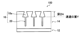
- FIG. 1 is a schematic cross-sectional view of a preferred embodiment of a lithographic printing plate support of the present invention.
- the lithographic printing plate support of the present invention comprises an aluminum plate and an anodized film formed thereon, and the micropores in the anodized film have large diameter holes with a large average diameter and a small average diameter.
- the small-diameter hole has a shape configured by being connected along the depth direction (the thickness direction of the film).
- the on-press developability and the printing durability which have been regarded as a trade-off relationship. Relationships can be reconciled at a higher level.
- FIG. 1A is a schematic cross-sectional view of an embodiment of a lithographic printing plate support of the present invention.
- the planographic printing plate support 10 shown in FIG. 1 has a laminated structure in which an aluminum plate 12 and an aluminum anodized film 14 (hereinafter also simply referred to as an anodized film) are laminated in this order.
- the anodized film 14 has micropores 16 extending from the surface thereof toward the aluminum plate 12, and the micropores 16 are composed of a large diameter hole portion 18 and a small diameter hole portion 20.
- the term micropore is a commonly used term representing the pore in the anodized film and does not define the size of the pore.
- the aluminum plate 12 (aluminum support) used in the present invention is a metal whose main component is aluminum that is dimensionally stable, and is made of aluminum or an aluminum alloy.
- an alloy plate containing aluminum as a main component and containing a trace amount of foreign elements, or a plastic film or paper laminated or vapor-deposited with aluminum (alloy) is selected.
- a composite sheet in which an aluminum sheet is bonded to a polyethylene terephthalate film as described in Japanese Patent Publication No. 48-18327 may be used.
- a plate made of aluminum or an aluminum alloy mentioned above is generically called an aluminum plate 12.
- the foreign elements contained in the aluminum alloy include silicon, iron, manganese, copper, magnesium, chromium, zinc, bismuth, nickel, titanium, etc., and the content of the foreign element in the alloy is 10% by mass or less.
- a pure aluminum plate is suitable.
- pure aluminum is difficult to manufacture in terms of smelting technology, it may contain a slightly different element.
- the composition of the aluminum plate 12 applied to the present invention is not specified, and conventionally known and used materials such as JISJA 1050, JIS A 1100, JIS A 3103, JIS A 3005, etc. Can be used as appropriate.
- the aluminum plate 12 used in the present invention is usually processed while continuously running in a web shape, and the width is about 400 mm to 2000 mm and the thickness is about 0.1 mm to 0.6 mm.
- the width and thickness can be changed as appropriate according to the size of the printing press, the size of the printing plate, and the desire of the user.
- the aluminum plate is appropriately subjected to substrate surface treatment as described below.
- the anodized film 14 is generally produced on the surface of the aluminum plate 12 by anodizing treatment, and is substantially perpendicular to the film surface, and has an anodized aluminum film having ultrafine micropores 16 that are uniformly distributed. Alumina film).
- the micropores 16 extend along the thickness direction (aluminum plate 12 side) from the surface of the anodized film opposite to the aluminum plate 12.
- the micropores 16 in the anodized film 14 include a large diameter hole 18 extending from the surface of the anodized film to an average depth of 75 to 120 nm (depth A: see FIG. 1), and a bottom of the large diameter hole 18.
- the small-diameter hole 20 extends from the communication position (communication position Y: see FIG. 1) to an average depth of 900 to 2000 nm. Below, the large diameter hole part 18 and the small diameter hole part 20 are explained in full detail.
- the average diameter (average opening diameter) of the large-diameter hole 18 on the surface of the anodized film 14 is 10 nm or more and less than 30 nm. Within such a range, excellent printing durability of a lithographic printing plate obtained using a lithographic printing plate support, and excellent printing durability and on-press developability of a lithographic printing plate precursor obtained using a support. Ink removal and neglectability are achieved. Of these, the average diameter is preferably 10 to 25 nm, more preferably 11 to 15 nm, and even more preferably 11 to 13 nm, from the viewpoint of more excellent printing durability.
- the diameter (diameter) of the micropore (large-diameter hole) is measured and averaged.
- a circle equivalent diameter is used.
- the “equivalent circle diameter” is a diameter of the circle when the shape of the opening is assumed to be a circle having the same projected area as the projected area of the opening.
- the bottom of the large-diameter hole 18 is located at an average depth of 75 to 120 nm (hereinafter also referred to as depth A) from the surface of the anodized film. That is, the large-diameter hole 18 is a hole extending from 75 to 120 nm in the depth direction (thickness direction) from the surface of the anodized film. Within such a range, excellent printing durability of the lithographic printing plate obtained using the lithographic printing plate support, and excellent on-press developability of the lithographic printing plate precursor obtained using the support are achieved. . Of these, the depth A is preferably 85 to 110 nm, more preferably 85 to 105 nm, from the viewpoint of more excellent printing durability and on-press developability.
- the measuring method of the cross section of an anodic oxide film can apply a well-known method (For example, an anodic oxide film is processed by FIB cutting, a thin film (about 50 nm) is produced, and the cross section of the anodic oxide film 14 is measured. ).
- the relationship (depth A / average diameter) between the average diameter of the large-diameter hole portion 18 and the depth A where the bottom portion is located satisfies the relationship of more than 4.0 and 12.0 or less. Within such a range, excellent printing durability of the lithographic printing plate obtained using the lithographic printing plate support, and excellent on-press developability of the lithographic printing plate precursor obtained using the support are achieved. . Of these, (depth A / average diameter) is preferably 5.6 to 10.0, more preferably 6.5 to 9.6, in terms of more excellent printing durability and on-press developability. More preferred.
- the shape of the large-diameter hole portion 18 is not particularly limited, and is substantially straight tubular (substantially cylindrical), an inverted conical shape (tapered shape) whose diameter decreases from the anodized film surface toward the aluminum plate 12 side, an anodized film Examples include a substantially conical shape (reverse taper shape) whose diameter increases from the surface toward the aluminum plate 12 side. Preferably, it is a substantially straight tube shape or a reverse taper shape.
- the inner diameter of the large-diameter hole 18 may have a difference of about 1 to 5 nm compared to the opening diameter on the surface of the anodized film 16.
- FIG. 2 shows a case where the large-diameter hole portion 18a has a substantially conical shape (reverse taper shape) whose diameter increases from the surface of the anodized film 14 toward the aluminum plate 12 side.
- the diameter (inner diameter) of the large-diameter hole 18a in the lithographic printing plate support 100 gradually increases from the surface of the anodized film 14 toward the aluminum plate 12 side.
- the shape of the large-diameter hole 18a is not particularly limited as long as the above-described diameter condition is satisfied, but is substantially conical or bell-shaped.
- the lithographic printing plate is excellent in various properties such as printing durability, neglectability, and ink repellency.
- the average diameter (surface layer average diameter) of the large-diameter hole 18a on the surface of the anodized film 14 is smaller than the average diameter (bottom average diameter) at the communication position Y with the small-diameter hole 20 of the large-diameter hole 18a.
- the size of the bottom average diameter is not particularly limited, but is preferably more than 10 nm and not more than 60 nm, and preferably 20 to 30 nm. Within this range, the lithographic printing plate is excellent in various properties such as neglectability, ink repellency, and on-press developability.
- the ratio of the bottom average diameter to the depth A is not particularly limited, but is preferably 1.2 or more and less than 12.0, and preferably 2.5 to 6.0. It is more preferable. Within such a range, the lithographic printing plate has excellent properties such as printing durability, neglectability, and ink repellency.
- a known method can be applied to the method for measuring the cross section of the anodized film. For example, the anodized film 14 is subjected to FIB cutting to produce a thin film (about 50 nm), and the cross section of the anodized film 14 is measured.
- the surface area increase magnification represented by the following formula (A) is preferably 1.9 to 16.0, and more preferably 2.1 to 11.7. . Within this range, the lithographic printing plate has excellent printing durability, neglectability, ink wiping property or on-press development property.
- “1” in the above formula (A) represents an area of 1 ⁇ m ⁇ 1 ⁇ m on the surface of the anodized film.
- “ ⁇ ⁇ (surface layer average diameter / 2 + bottom average diameter / 2) ⁇ ((bottom average diameter / 2 ⁇ surface layer average diameter / 2) 2 + depth A 2 ) 1/2 ” is a large-diameter hole.
- “ ⁇ x (bottom average diameter / 2) 2 " represents the area of the bottom surface of the large-diameter hole
- “ ⁇ x (surface layer average diameter / 2) 2 " represents the large-diameter hole. It represents the area of the opening on the surface of the anodized film.
- the shape of the bottom of the large-diameter hole 18 is not particularly limited, and may be a curved surface (convex shape) or a planar shape.
- the small-diameter hole 20 is a hole that communicates with the bottom of the large-diameter hole 18 and extends further in the depth direction (thickness direction) than the communication position Y.
- One small-diameter hole 20 normally communicates with one large-diameter hole 18, but two or more small-diameter holes 20 may communicate with the bottom of one large-diameter hole 18.
- the average diameter at the communication position of the small-diameter hole 20 is greater than 0 and less than 10.0 nm.
- the average diameter is preferably 9.5 nm or less, and more preferably 9.0 nm or less, from the viewpoint that the on-press development property, ink repellency, or neglectability is more excellent.
- the average diameter is 10.0 nm or more, the printing durability of the lithographic printing plate using the lithographic printing plate support of the present invention and the on-press developability of the lithographic printing plate precursor are poor.
- the average diameter of the small-diameter portion 20, the anodized film 14 surface was observed N 4 sheets at a magnification 150,000 ⁇ FE-SEM, the four images obtained are present in a range of 400 ⁇ 600 nm 2 Micro It is a value obtained by measuring and averaging the diameter (diameter) of the pore (small-diameter hole).
- the upper part of the anodic oxide film 14 region having the large-diameter hole
- is cut for example, cut with argon gas
- the average diameter of the small diameter holes may be obtained by observing the surface with the FE-SEM.
- an equivalent circle diameter is used.
- the “equivalent circle diameter” is a diameter of the circle when the shape of the opening is assumed to be a circle having the same projected area as the projected area of the opening.
- the bottom of the small-diameter hole 20 is located at a place extending 900 to 2000 nm further in the depth direction from the communication position with the large-diameter hole 18 (corresponding to the depth A described above).
- the small-diameter hole 20 is a hole extending further in the depth direction (thickness direction) from the communication position with the large-diameter hole 18, and the average depth of the small-diameter hole 20 is 900 to 2000 nm.
- the bottom is preferably located at a location extending 900 to 1500 nm from the communicating position. When the average depth is less than 900 nm, the scratch resistance of the lithographic printing plate support is poor.
- the average depth is a value obtained by taking a photograph (50,000 times) of the cross section of the anodic oxide film 14 observed by FE-SEM and measuring the depths of 25 or more small-diameter holes.
- the ratio of the average diameter at the communication position of the small-diameter hole 20 and the average diameter of the large-diameter hole 18 on the surface of the anodized film is not particularly limited, but is more than 1.00 1 Is preferably .50 or less, more preferably 1.10 to 1.40, and even more preferably 1.10 to 1.30. Within the above range, the lithographic printing plate has better printing durability or on-press developability.
- the density of the small-diameter hole 20 in the cross section of the anodized film 14 at the communication position Y is not particularly limited, but is preferably 100 to 5000 / ⁇ m 2 , and more preferably 600 to 1200 / ⁇ m 2 . Within this range, the on-press developability, ink repellency, or neglectability of the lithographic printing plate is further improved.
- the shape of the small-diameter hole 20 is not particularly limited, and includes a substantially straight tube (substantially cylindrical shape), a conical shape whose diameter decreases in the depth direction, and the like, preferably a substantially straight tube.
- the small-diameter hole 20 may be a hole extending from the communication position Y while branching toward the aluminum plate 12.
- the shape of the bottom part of the small diameter hole part 20 is not specifically limited, A curved surface shape (convex shape) may be sufficient, and planar shape may be sufficient.
- the inner diameter of the small-diameter hole 20 is not particularly limited, but is usually the same size as the diameter at the communication position, or may be smaller or larger than the diameter.
- the inner diameter of the small-diameter hole 20 may usually have a difference of about 1 to 10 nm from the diameter of the opening.
- the thickness of the anodized film from the bottom of the small-diameter hole 20 to the surface of the aluminum plate 12 is not particularly limited, but is preferably 7 to 50 nm, More preferably.
- the portion of the anodized film located at the thickness X is sometimes called a barrier layer. If the thickness X is in the above range, fine spot dirt is more excellent.
- the numerical value of the thickness X is an average value, and is a value obtained by measuring the thickness of the anodized film from the bottom of the small-diameter hole 20 at 50 or more locations to the surface of the aluminum plate 12 and arithmetically averaging them.
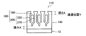
- the planographic printing plate support 110 has a laminated structure in which an aluminum plate 12 and an anodized aluminum film 140 are laminated in this order.
- the anodized film 140 has a micropore 160 extending from the surface thereof toward the aluminum plate 12, and the micropore 160 is composed of a large diameter hole portion 180 and a small diameter hole portion 200.
- the large-diameter hole portion 180 has a substantially conical shape (reverse taper shape) whose diameter increases from the surface of the anodized film 14 toward the aluminum plate 12 as described with reference to FIG.
- Various ranges such as the surface layer average diameter, bottom average diameter, ratio (depth A / bottom average diameter), and surface area increase ratio of the large-diameter hole portion 180 are as described above.
- the small-diameter hole 200 is a hole that communicates with the bottom of the large-diameter hole 180 and extends further in the depth direction (thickness direction) than the communication position Y.
- two small-diameter holes 200 communicate with one large-diameter hole 180, but the present invention is not limited to this mode, and one small-diameter hole 200 communicates with one large-diameter hole 180.
- two or more small-diameter holes 200 may communicate with one large-diameter hole 180.
- the average diameter at the communication position of the small-diameter hole portion 200 is synonymous with the average diameter of the small-diameter hole portion 20, and the preferred range is also the same.
- the average depth of the small diameter hole portion 200 is synonymous with the average depth of the small diameter hole portion 20, and the preferred range is also the same.
- the ratio of the average diameter at the communication position of the small-diameter hole portion 200 to the average diameter of the large-diameter hole portion 180 at the surface of the anodized film is the average at the communication position of the small-diameter hole portion 20. It is synonymous with the ratio of the diameter and the average diameter of the large-diameter hole 18 on the surface of the anodized film (large-diameter hole diameter / small-diameter hole diameter), and the preferred range is also the same.
- the small diameter hole portion 200 includes a first small diameter hole portion 210 and a second small diameter hole portion 220 having different average depths.
- the average depth of the first small diameter hole portion 210 is deeper than the average depth of the second small diameter hole portion 220. That is, the bottom portion of the first small diameter hole portion 210 is located closer to the aluminum plate 12 than the bottom portion of the second small diameter hole portion 220.
- the calculation method of the average depth of the 1st small diameter hole part 210 and the 2nd small diameter hole part 220 is as follows.
- the shortest small-diameter hole (hereinafter referred to as the smallest small-diameter hole) and the longest small-diameter hole (hereinafter referred to as the largest small-diameter hole) are selected from the small-diameter holes, and the position of the bottom of one small-diameter hole is selected. Is selected as the second small-diameter hole when the position is close to the bottom of the smallest small-diameter hole, and the first small-diameter hole is selected when the position of the bottom of one small-diameter hole is close to the bottom of the largest small-diameter hole Selected as part.
- the position of the bottom part of one small diameter hole part is located between the position of the bottom part of the smallest small diameter hole part and the position of the bottom part of the largest small diameter hole part, it is selected as the first small diameter hole part.
- At least 25 depths of the small-diameter holes selected as the first small-diameter hole are measured, and they are arithmetically averaged to measure the average depth of the first small-diameter hole.
- at least 25 depths of the small-diameter holes selected as the second small-diameter holes are measured, and they are arithmetically averaged to measure the average depth of the second small-diameter holes.
- the difference between the average depth of the first small-diameter hole portion 210 and the average depth of the second small-diameter hole portion 220 is not particularly limited, but is preferably 75 to 200 nm, more preferably 100 to 200 nm is more preferable.
- the density of the small-diameter hole portion 200 in the cross section of the anodized film 140 at the communication position Y is not particularly limited, but is preferably 100 to 5000 / ⁇ m 2 , and more preferably 600 to 1200 / ⁇ m 2 . Within this range, the on-press developability, ink repellency, or neglectability of the lithographic printing plate is further improved.
- the density of the first small-diameter hole 210 is not particularly limited, but is preferably 550 to 700 / ⁇ m 2, and more preferably 550 to 650 / ⁇ m 2 in terms of better resistance to pot-like dirt.
- the average thickness X of the anodic oxide film from the bottom of the first small-diameter hole 210 to the surface of the aluminum plate 12 is not particularly limited, but is preferably 17 nm or more, more preferably 18 nm or more in terms of more excellent spot-like stain resistance. Is more preferable.
- the upper limit is not particularly limited, but is usually 30 nm or less in many cases.
- the said average thickness is the value which measured the thickness of the anodic oxide film from the bottom part of the 1st small diameter hole part 210 of 50 or more places to the aluminum plate 12, and arithmetically averaged them.
- the minimum thickness of the anodized film from the bottom of the first small-diameter hole 210 to the surface of the aluminum plate 12 is not particularly limited, but is preferably 15 nm or more, and more preferably 17 nm or more.
- the shape of the first small-diameter hole portion 210 and the second small-diameter hole portion 220 is not particularly limited, and examples thereof include a substantially straight tubular shape (substantially cylindrical shape).
- the first small-diameter hole portion 210 has a larger inner diameter (for example, about 1 to 10 nm larger) in the region on the aluminum plate 12 side from the position where the bottom of the second small-diameter hole portion 220 is located. It may be.
- Step of anodizing aluminum plate Step of anodizing aluminum plate (third anodizing step) Step of anodizing aluminum plate obtained in second anodizing step (hydrophilizing step) Obtained in second or third anodizing step
- the process of performing a hydrophilization treatment on the aluminum plate thus obtained will be described in detail below. Note that the roughening treatment step, the pore wide treatment step, the hydrophilization treatment step, and the third anodizing treatment step may be omitted if not necessary.
- FIG. 3 is a schematic cross-sectional view of the substrate and the anodic oxide film showing the order from the first anodizing process to the third anodizing process.
- the roughening treatment step is a step of subjecting the surface of the aluminum plate to a roughening treatment including an electrochemical roughening treatment. This step is preferably performed before the first anodizing step described later, but may not be performed as long as the surface of the aluminum plate already has a preferable surface shape.
- the surface roughening treatment may be performed only by electrochemical surface roughening treatment, but may be performed by combining electrochemical surface roughening treatment with mechanical surface roughening treatment and / or chemical surface roughening treatment. Also good. When the mechanical surface roughening treatment and the electrochemical surface roughening treatment are combined, it is preferable to perform the electrochemical surface roughening treatment after the mechanical surface roughening treatment.
- the electrochemical surface roughening treatment is preferably performed in an aqueous solution of nitric acid or hydrochloric acid.
- the mechanical roughening treatment is generally performed for the purpose of setting the surface of the aluminum plate to a surface roughness Ra : 0.35 to 1.0 ⁇ m.
- the conditions for the mechanical surface roughening treatment are not particularly limited, but for example, it can be applied according to the method described in Japanese Patent Publication No. 50-40047.
- the mechanical surface roughening treatment can be performed by brush grain processing using a pumiston suspension or can be performed by a transfer method.
- the chemical surface roughening treatment is not particularly limited, and can be performed according to a known method.
- the following chemical etching treatment is preferably performed.
- the chemical etching process performed after the mechanical roughening process smoothes the uneven edges of the surface of the aluminum plate, prevents ink from being caught during printing, and improves the stain resistance of the lithographic printing plate At the same time, it is performed to remove unnecessary materials such as abrasive particles remaining on the surface.
- acid etching or alkali etching is known, but as a method that is particularly excellent in terms of etching efficiency, chemical etching treatment using an alkaline solution (hereinafter also referred to as “alkali etching treatment”). ).
- the alkaline agent used in the alkaline solution is not particularly limited, and preferred examples include caustic soda, caustic potash, sodium metasilicate, sodium carbonate, sodium aluminate, and sodium gluconate. Each alkaline agent may contain aluminum ions.
- the concentration of the alkaline solution is preferably 0.01% by mass or more, more preferably 3% by mass or more, more preferably 30% by mass or less, and more preferably 25% by mass or less. preferable.
- the temperature of the alkaline solution is preferably room temperature or higher, more preferably 30 ° C. or higher, preferably 80 ° C. or lower, and more preferably 75 ° C. or lower.
- the etching amount is preferably 0.1 g / m 2 or more, more preferably 1 g / m 2 or more, more preferably 20 g / m 2 or less, and 10 g / m 2 or less. Is more preferable.
- the treatment time is preferably 2 seconds to 5 minutes corresponding to the etching amount, and more preferably 2 to 10 seconds from the viewpoint of improving productivity.
- a chemical etching treatment (hereinafter referred to as “desmut treatment”) is performed using a low-temperature acidic solution in order to remove products generated by the alkali etching treatment. It is also preferable to apply.
- the acid used for an acidic solution is not specifically limited, For example, a sulfuric acid, nitric acid, and hydrochloric acid are mentioned.
- the concentration of the acidic solution is preferably 1 to 50% by mass.
- the temperature of the acidic solution is preferably 20 to 80 ° C. When the concentration and temperature of the acidic solution are within this range, the spot-like stain resistance of the lithographic printing plate using the lithographic printing plate support of the present invention is further improved.
- the roughening process is a process of applying an electrochemical roughening process after performing a mechanical roughening process and a chemical etching process as desired.
- the chemical etching treatment can be performed using an alkaline aqueous solution such as caustic soda before the electrochemical surface roughening treatment. Thereby, impurities existing in the vicinity of the surface of the aluminum plate can be removed.
- the electrochemical roughening treatment is suitable for making a lithographic printing plate having excellent printability because it is easy to impart fine irregularities (pits) to the surface of the aluminum plate.
- the electrochemical surface roughening treatment is performed using direct current or alternating current in an aqueous solution mainly composed of nitric acid or hydrochloric acid.
- the following chemical etching treatment after the electrochemical surface roughening treatment.
- Smut and intermetallic compounds exist on the surface of the aluminum plate after the electrochemical roughening treatment.
- the chemical etching process performed after the electrochemical surface roughening process it is preferable to first perform a chemical etching process (alkali etching process) using an alkaline solution in order to efficiently remove smut.
- the treatment temperature is preferably 20 to 80 ° C.
- the treatment time is preferably 1 to 60 seconds.
- a chemical etching treatment using an alkaline solution is performed, and then a chemical etching treatment (desmut treatment) is performed using a low-temperature acidic solution in order to remove the resulting products. Is preferred. Even when the alkali etching treatment is not performed after the electrochemical surface roughening treatment, it is preferable to perform a desmut treatment in order to efficiently remove the smut.
- any of the above-described chemical etching treatments can be performed by a dipping method, a shower method, a coating method, or the like, and is not particularly limited.
- the aluminum plate having the micropores extending in the depth direction (thickness direction) is formed on the surface of the aluminum plate by anodizing the aluminum plate subjected to the roughening treatment. This is a step of forming a film.
- an aluminum anodic oxide film 14a having micropores 16a is formed on the surface of the aluminum plate 12, as shown in FIG.
- the first anodizing treatment can be performed by a method conventionally performed in this field, but manufacturing conditions are appropriately set so that the above-described micropore 16 can be finally formed.
- the average diameter (average opening diameter) of the micropores 16a formed in the first anodizing treatment step is usually about 4 to 14 nm, preferably 5 to 10 nm. If it is in the said range, the micropore 16 which has the predetermined shape mentioned above will be easy to form, and the performance of the obtained lithographic printing plate and lithographic printing plate precursor will be more excellent.
- the depth of the micropore 16a is usually about 65 to 110 nm, preferably 75 to 95 nm. If it is in the said range, the micropore 16 which has the predetermined shape mentioned above will be easy to form, and the performance of the obtained lithographic printing plate and lithographic printing plate precursor will be more excellent.
- the pore density of the micropores 16a is not particularly limited, but the pore density is preferably 50 to 4000 / ⁇ m 2 , and more preferably 100 to 3000 / ⁇ m 2 . Within the above range, the resulting lithographic printing plate is excellent in printing durability and neglectability and on-press developability of the lithographic printing plate precursor.
- the thickness of the anodized film obtained by the first anodizing treatment step is preferably 75 to 120 nm, more preferably 85 to 105 nm. If it is within the above range, the printing durability of the lithographic printing plate using the lithographic printing plate support obtained through the step, neglectability, pot stain resistance, and round white spot resistance, and Excellent on-press developability of lithographic printing plate precursor. Further, the coating amount of the anodized film obtained by the first anodizing treatment step is preferably 0.18 to 0.29 g / m 2 , more preferably 0.2 to 0.25 g / m 2 . If it is within the above range, the printing durability of the lithographic printing plate using the lithographic printing plate support obtained through the step, neglectability, pot stain resistance, and round white spot resistance, and Excellent on-press developability of lithographic printing plate precursor.
- an aqueous solution of sulfuric acid, phosphoric acid, oxalic acid or the like can be mainly used as an electrolytic bath.
- chromic acid, sulfamic acid, benzenesulfonic acid, etc., or an aqueous solution or a non-aqueous solution combining two or more of these may be used.
- direct current or alternating current is passed through the aluminum plate in the electrolytic bath as described above, an anodized film can be formed on the surface of the aluminum plate.
- the electrolytic bath may contain aluminum ions.
- the content of aluminum ions is not particularly limited, but is preferably 1 to 10 g / L.
- the conditions of the anodizing treatment are appropriately set depending on the electrolytic solution used.
- the concentration of the electrolytic solution is 1 to 80% by mass (preferably 5 to 20% by mass)
- the liquid temperature is 5 to 70 ° C. ( Preferably 10 to 60 ° C.)
- current density 0.5 to 60 A / dm 2 (preferably 5 to 50 A / dm 2 )
- voltage 1 to 100 V preferably 5 to 50 V
- electrolysis time 1 to 100 seconds preferably The range of 5 to 60 seconds is appropriate.
- the pore wide treatment step is a treatment (pore diameter enlargement treatment) for enlarging the diameter (pore diameter) of the micropores present in the anodized film formed by the first anodizing treatment step described above.
- the average diameter of the micropores 16b is preferably expanded to a range of 10 nm or more and less than 30 nm.
- the micropore 16b is a portion corresponding to the large-diameter hole 18 described above. Moreover, it is preferable to adjust so that the average depth from the surface of the micropore 16b may become comparable with the depth A mentioned above by this process.
- the pore-wide treatment is performed by bringing the aluminum plate obtained by the above-described first anodizing treatment step into contact with an acid aqueous solution or an alkali aqueous solution.
- the method of making it contact is not specifically limited, For example, the immersion method and the spray method are mentioned. Of these, the dipping method is preferred.
- an alkaline aqueous solution When an alkaline aqueous solution is used in the pore wide treatment step, it is preferable to use at least one alkaline aqueous solution selected from the group consisting of sodium hydroxide, potassium hydroxide, and lithium hydroxide.
- the concentration of the alkaline aqueous solution is preferably 0.1 to 5% by mass.
- the aluminum plate After adjusting the pH of the alkaline aqueous solution to 11 to 13, the aluminum plate is placed in the alkaline aqueous solution for 1 to 300 seconds (preferably 1 to 50 seconds) under the condition of 10 to 70 ° C. (preferably 20 to 50 ° C.). It is appropriate to make it contact.
- the alkali treatment liquid may contain a metal salt of a polyvalent weak acid such as carbonate, borate or phosphate.
- an aqueous acid solution When an aqueous acid solution is used in the pore-wide treatment step, it is preferable to use an aqueous solution of an inorganic acid such as sulfuric acid, phosphoric acid, nitric acid, hydrochloric acid, or a mixture thereof.
- the concentration of the acid aqueous solution is preferably 1 to 80% by mass, more preferably 5 to 50% by mass. It is appropriate that the aluminum plate is brought into contact with the acid aqueous solution for 1 to 300 seconds (preferably 1 to 150 seconds) under the condition that the aqueous solution of the acid aqueous solution is 5 to 70 ° C. (preferably 10 to 60 ° C.).
- the alkaline aqueous solution or the acidic aqueous solution may contain aluminum ions.
- the content of aluminum ions is not particularly limited, but is preferably 1 to 10 g / L.
- the second anodizing treatment step is a step of forming micropores extending in the depth direction (thickness direction) by subjecting the aluminum plate subjected to the above-described pore wide treatment to anodizing treatment.
- an anodized film 14c having micropores 16c extending in the depth direction is formed as shown in FIG.
- the average diameter is communicated with the bottom of the micropore 16b, the average diameter is smaller than the average diameter of the micropore 16b (corresponding to the large diameter hole 18), and the depth from the communicating position.
- a new hole extending in the direction is formed. The hole corresponds to the small diameter hole 20 described above.
- the average diameter of the newly formed hole is greater than 0 and less than 10 nm, and the average depth from the communication position with the large diameter hole 18 is within the predetermined range described above. Processing is performed.
- the electrolytic bath used for the treatment is the same as that in the first anodizing treatment step, and the treatment conditions are appropriately set according to the material used.
- the conditions of the anodizing treatment are appropriately set depending on the electrolytic solution used. In general, the concentration of the electrolytic solution is 1 to 80% by mass (preferably 5 to 20% by mass), and the liquid temperature is 5 to 70 ° C.
- the film thickness of the anodized film obtained by the second anodizing treatment step is usually 900 to 2000 nm, preferably 900 to 1500 nm.
- the lithographic printing plate using the lithographic printing plate support obtained through this step is excellent in printing durability and neglectability, and on-press developability of the lithographic printing plate precursor.
- the coating amount of the anodized film obtained by the second anodizing treatment step is usually 2.2 to 5.4 g / m 2 , preferably 2.2 to 4.0 g / m 2 .
- the lithographic printing plate using the lithographic printing plate support obtained through this step is excellent in printing durability and neglectability, and on-press developability of the lithographic printing plate precursor.
- Ratio (film thickness 1 / film thickness) of the thickness of the anodized film obtained by the first anodizing process (film thickness 1) and the thickness of the anodized film obtained by the second anodizing process (film thickness 2) 2) is preferably from 0.01 to 0.15, more preferably from 0.02 to 0.10. Within the above range, the lithographic printing plate support is excellent in scratch resistance.
- the voltage may increase the voltage to apply stepwise or continuously during the process of a 2nd anodizing process. As the applied voltage increases, the diameter of the hole to be formed increases. Note that, by increasing the voltage applied in the second anodizing treatment step, the thickness of the anodized film between the bottom of the obtained small diameter hole and the aluminum plate tends to increase. If the anodized film between the bottom of the small-diameter hole and the aluminum plate has a predetermined thickness by performing the above-described treatment, the third anodizing treatment step described later may not be performed. .
- the anodizing treatment is mainly performed between the bottom of the small-diameter hole and the aluminum plate by further anodizing the aluminum plate subjected to the second anodizing treatment.
- This is a step of increasing the thickness of the coating (the thickness of the barrier layer).
- the thickness X becomes a predetermined size as shown in FIG.
- the third anodizing process need not be performed.
- the conditions of the anodizing treatment in the third anodizing treatment step are appropriately set depending on the electrolyte used, but usually, the treatment is performed at a voltage higher than the voltage applied in the second anodizing treatment step.
- the kind of electrolyte solution used is not specifically limited, The electrolyte solution mentioned above can be used.
- the thickness X can be efficiently increased without changing the shape of the small-diameter hole portion obtained by the second anodizing treatment.
- the coating amount of the anodized film obtained by the third anodizing treatment step is usually 0.13 to 0.65 g / m 2 , preferably 0.26 to 0.52 g / m 2 . If it is within the above range, the printing durability of the lithographic printing plate using the lithographic printing plate support obtained through the step, neglectability, pot stain resistance, and round white spot resistance, and Excellent on-press developability of lithographic printing plate precursor.
- micropores may extend further to the aluminum side by performing the third anodizing treatment step.
- the method for producing a lithographic printing plate support of the present invention may have a hydrophilization treatment step in which a hydrophilization treatment is performed after the second or third anodizing treatment step described above.
- a hydrophilization treatment a known method disclosed in paragraphs [0109] to [0114] of JP-A-2005-254638 can be used.
- Hydrophilization by a method of immersing in an aqueous solution of an alkali metal silicate such as sodium silicate or potassium silicate, or a method of forming a hydrophilic undercoat layer by applying a hydrophilic vinyl polymer or hydrophilic compound. It is preferable to carry out the treatment.
- an alkali metal silicate such as sodium silicate or potassium silicate
- Hydrophilization treatment with an aqueous solution of an alkali metal silicate such as sodium silicate and potassium silicate is described in US Pat. No. 2,714,066 and US Pat. No. 3,181,461. It can be performed according to methods and procedures.
- the lithographic printing plate support of the present invention is preferably a lithographic printing plate support obtained by subjecting the above-described aluminum plate to the treatments shown in the following A and B aspects in the order shown below. From the viewpoint of printing durability, the A mode is particularly preferable. In addition, it is desirable to perform water washing between the following processes. However, when two steps (processes) to be performed in succession use a liquid having the same composition, washing with water may be omitted.
- the process (1) may implement a mechanical surface roughening process as needed before the process of (2) of the said A aspect and B aspect. From the viewpoint of printing durability and the like, it is preferable that the process (1) is not included in each embodiment.
- the mechanical surface roughening treatment, electrochemical surface roughening treatment, chemical etching treatment, anodizing treatment and hydrophilization treatment in the above (1) to (12) are the same as the above-described treatment methods and conditions. However, the treatment is preferably performed under the treatment method and conditions described below.
- the mechanical roughening treatment is preferably mechanically roughened with a rotating nylon brush roll having a bristle diameter of 0.2 to 1.61 mm and a slurry liquid supplied to the surface of the aluminum plate.
- a well-known thing can be used as an abrasive
- the specific gravity of the slurry liquid is preferably 1.05 to 1.3.
- a method of spraying a slurry liquid, a method of using a wire brush, a method of transferring the surface shape of an uneven rolling roll to an aluminum plate, or the like may be used.
- the concentration of the alkaline aqueous solution used for the chemical etching treatment in the alkaline aqueous solution is preferably 1 to 30% by mass, and 0 to 10% by mass of the alloy component contained in aluminum and the aluminum alloy may be contained.
- an aqueous solution mainly composed of caustic soda is particularly preferable.
- the liquid temperature is preferably from room temperature to 95 ° C. and is preferably treated for 1 to 120 seconds. After the etching process is completed, it is preferable to perform liquid draining with a nip roller and water washing with a spray so as not to bring the processing liquid into the next process.
- the dissolution amount of the aluminum plate in the first alkaline etching treatment is preferably 0.5 to 30 g / m 2 , more preferably 1.0 to 20 g / m 2 , and 3.0 to 15 g / m 2. More preferably.
- the amount of dissolution of the aluminum plate in the second alkali etching treatment is preferably 0.001 to 30 g / m 2 , more preferably 0.1 to 4 g / m 2 , and 0.2 to 1.5 g / m 2. even more preferably in the range of m 2.
- the amount of dissolution of the aluminum plate in the third alkali etching treatment is preferably 0.001 to 30 g / m 2 , more preferably 0.01 to 0.8 g / m 2 , and 0.02 to 0.00. More preferably, it is 3 g / m 2 .
- the chemical etching treatment in an acidic aqueous solution, phosphoric acid, nitric acid, sulfuric acid, chromic acid, hydrochloric acid, or a mixed acid containing two or more acids thereof is preferably used.
- the concentration of the acidic aqueous solution is preferably 0.5 to 60% by mass. Further, in the acidic aqueous solution, 0 to 5% by mass of aluminum and an alloy component contained in the aluminum alloy may be dissolved.
- the liquid temperature is from room temperature to 95 ° C., and the treatment time is preferably 1 to 120 seconds. After the desmut treatment is completed, it is preferable to perform liquid draining with a nip roller and water washing with a spray so as not to bring the treatment liquid into the next step.
- the aqueous solution used for the electrochemical surface roughening treatment will be described.
- the aqueous solution mainly composed of nitric acid used in the first electrochemical surface roughening treatment one used for an ordinary electrochemical surface roughening treatment using direct current or alternating current can be used, and an aqueous nitric acid solution of 1 to 100 g / L. 1 to 1 g / L to saturation of one or more of hydrochloric acid or nitric acid compound having nitrate ions such as aluminum nitrate, sodium nitrate, ammonium nitrate; hydrochloric acid ions such as aluminum chloride, sodium chloride, ammonium chloride; be able to.
- the metal contained in aluminum alloys such as iron, copper, manganese, nickel, titanium, magnesium, and a silica, may melt
- the temperature is preferably 10 to 90 ° C, more preferably 40 to 80 ° C.
- the aqueous solution mainly composed of hydrochloric acid used in the second electrochemical surface roughening treatment can be the one used for the normal surface roughening treatment using direct current or alternating current, and can be 1 to 100 g / L.
- hydrochloric acid ions such as aluminum chloride, sodium chloride and ammonium chloride
- the metal contained in aluminum alloys such as iron, copper, manganese, nickel, titanium, magnesium, and a silica, may melt
- the temperature is preferably 10 to 60 ° C., more preferably 20 to 50 ° C. Hypochlorous acid may be added.
- the aqueous solution mainly composed of hydrochloric acid used in the electrochemical surface roughening treatment in the aqueous hydrochloric acid solution in the embodiment B can be used for the electrochemical surface roughening treatment using ordinary direct current or alternating current, It can be used by adding 0-30 g / L of sulfuric acid to 1-100 g / L hydrochloric acid aqueous solution. Also, to this solution, add one or more of hydrochloric acid or nitric acid compound having nitrate ions such as aluminum nitrate, sodium nitrate, ammonium nitrate; hydrochloric acid ions such as aluminum chloride, sodium chloride, ammonium chloride, etc.
- the metal contained in aluminum alloys such as iron, copper, manganese, nickel, titanium, magnesium, and a silica, may melt
- a solution obtained by adding aluminum chloride, aluminum nitrate or the like so that the aluminum ion is 3 to 50 g / L in a 0.5 to 2% by mass nitric acid aqueous solution.
- the temperature is preferably 10 to 60 ° C., more preferably 20 to 50 ° C. Hypochlorous acid may be added.
- Sine wave, rectangular wave, trapezoidal wave, triangular wave, etc. can be used as the alternating current power supply waveform for electrochemical roughening treatment.
- the frequency is preferably 0.1 to 250 Hz.
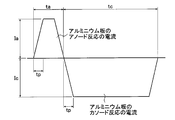
- FIG. 4 is a graph showing an example of an alternating waveform current waveform diagram used for an electrochemical roughening treatment in the method for producing a lithographic printing plate support of the present invention.
- ta is the anode reaction time
- tc is the cathode reaction time
- tp is the time until the current reaches the peak from
- Ia is the peak current on the anode cycle side
- Ic is the peak current on the cathode cycle side. It is.
- the time tp until the current reaches a peak from 0 is preferably 1 to 10 msec.
- tp Due to the influence of the impedance of the power supply circuit, if tp is less than 1, a large power supply voltage is required at the rise of the current waveform, and the equipment cost of the power supply increases. When it is longer than 10 msec, it is easily affected by a trace component in the electrolytic solution, and uniform surface roughening is difficult to be performed.
- the condition of one cycle of alternating current used for electrochemical surface roughening is that the ratio tc / ta of the anode reaction time ta to the cathode reaction time tc of the aluminum plate is 1 to 20, the quantity of electricity Qc when the aluminum plate is anode and the anode It is preferable that the ratio Qc / Qa of the amount of electricity Qa is 0.3 to 20 and the anode reaction time ta is 5 to 1000 msec. More preferably, tc / ta is 2.5-15. Qc / Qa is more preferably 2.5 to 15.
- the current density is preferably 10 to 200 A / dm 2 for both the anode cycle side Ia and the cathode cycle side Ic of the current at the peak value of the trapezoidal wave.
- Ic / Ia is preferably in the range of 0.3 to 20.
- the total amount of electricity involved in the anode reaction of the aluminum plate at the end of electrochemical roughening is preferably 25 to 1000 C / dm 2 .
- electrolytic cell used for electrochemical surface roughening using alternating current known electrolytic cells such as a vertical type, a flat type, and a radial type can be used.
- a radial electrolytic cell as described in Japanese Patent No. 195300 is particularly preferred.
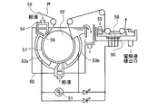
- FIG. 5 is a side view showing an example of a radial type cell in an electrochemical surface roughening treatment using alternating current in the method for producing a lithographic printing plate support of the present invention.
- 50 is a main electrolytic cell
- 51 is an AC power source
- 52 is a radial drum roller
- 53a and 53b are main electrodes
- 54 is an electrolyte supply port
- 55 is an electrolyte
- 56 is a slit
- 57 is an electrolyte passage
- 58 is an auxiliary anode
- 60 is an auxiliary anode tank
- W is an aluminum plate.
- the electrolysis conditions may be the same or different.
- the aluminum plate W is wound around a radial drum roller 52 disposed so as to be immersed in the main electrolytic cell 50, and is subjected to electrolytic treatment by main electrodes 53a and 53b connected to the AC power source 51 in the course of conveyance.
- the electrolytic solution 55 is supplied from the electrolytic solution supply port 54 to the electrolytic solution passage 57 between the radial drum roller 52 and the main poles 53a and 53b through the slit 56.
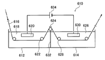
- the aluminum plate W treated in the main electrolytic cell 50 is then subjected to electrolytic treatment in the auxiliary anode cell 60.
- An auxiliary anode 58 is disposed opposite to the aluminum plate W in the auxiliary anode tank 60, and the electrolytic solution 55 is supplied so as to flow in the space between the auxiliary anode 58 and the aluminum plate W.
- a direct current is applied between the aluminum plate and the electrode facing the aluminum plate to electrochemically roughen the surface. There may be.
- Drying step After obtaining the lithographic printing plate support obtained by the steps described above, it is preferable to perform a treatment (drying step) for drying the surface of the lithographic printing plate support before providing an image recording layer described later. Drying is preferably performed after the final treatment of the surface treatment, after washing with water and draining with a nip roller. Specific conditions are not particularly limited, but drying by hot air (50 to 200 ° C.) or a cold air natural drying method is preferable.
- the lithographic printing plate support of the present invention can be provided with an image recording layer such as a photosensitive layer and a heat-sensitive layer exemplified below to form the lithographic printing plate precursor of the present invention.
- the image recording layer is not particularly limited.
- conventional positive type, conventional negative type, photopolymer type (photopolymerization type photosensitive composition) described in paragraphs [0042] to [0198] of JP-A-2003-1956 Preferably), a thermal positive type, a thermal negative type, and an unprocessable type capable of on-machine development.
- a suitable image recording layer will be described in detail.
- a preferred image recording layer that can be used in the lithographic printing plate precursor according to the present invention is a layer that can be removed by printing ink and / or fountain solution.
- the image recording layer preferably has a polymerizable compound and can be recorded by infrared irradiation.
- it may be an image recording layer having thermoplastic polymer particles and an infrared absorber and capable of recording by infrared irradiation, and the image recording layer may have a polyglycerol compound.
- the exposed portion of the image recording layer is cured by infrared irradiation to form a hydrophobic (lipophilic) region, and the unexposed portion is dampened with water, ink or ink at the start of printing. It is quickly removed from the support by an emulsion of fountain solution and ink.
- each component of the image recording layer will be described.
- an image recording layer having an infrared absorber, a polymerization initiator, and a polymerizable compound, which can be recorded by infrared irradiation (Infrared absorber)
- Infrared absorber When forming an image of the lithographic printing plate precursor according to the present invention using a laser emitting an infrared ray of 760 to 1200 nm as a light source, an infrared absorber is usually used.
- the infrared absorber has a function of converting the absorbed infrared ray into heat and a function of being excited by the infrared ray and transferring electrons / energy to a polymerization initiator (radical generator) described later.
- the infrared absorber that can be used in the present invention is a dye or pigment having an absorption maximum at a wavelength of 760 to 1200 nm.
- dyes commercially available dyes, for example, known dyes described in documents such as “Dye Handbook” (edited by the Society for Synthetic Organic Chemistry, published in 1970) can be used. Specifically, dyes such as azo dyes, metal complex azo dyes, pyrazolone azo dyes, naphthoquinone dyes, anthraquinone dyes, phthalocyanine dyes, carbonium dyes, quinoneimine dyes, methine dyes, cyanine dyes, squarylium dyes, pyrylium salts, metal thiolate complexes, etc. Is mentioned. For example, the dyes disclosed in paragraphs [0096] to [0107] of JP2009-255434A can be suitably used.
- pigments described in paragraphs [0108] to [0112] of JP2009-255434A can be used.
- the polymerization initiator is a compound that generates radicals by energy of light, heat, or both, and initiates and accelerates polymerization of a compound having a polymerizable unsaturated group. In the present invention, radicals are generated by heat. It is preferable to use a compound (thermal radical generator).
- a known thermal polymerization initiator a compound having a bond with a small bond dissociation energy, a photopolymerization initiator, or the like can be used.
- polymerization initiator for example, polymerization initiators described in paragraphs [0115] to [0141] of JP-A-2009-255434 can be used.
- An onium salt or the like can be used as a polymerization initiator, and the oxime ester compound, diazonium salt, iodonium salt, or sulfonium salt is preferable from the viewpoint of reactivity and stability.
- These polymerization initiators are added in a proportion of 0.1 to 50% by mass, preferably 0.5 to 30% by mass, particularly preferably 1 to 20% by mass, based on the total solid content constituting the image recording layer. Can do. Within this range, good sensitivity and good stain resistance of the non-image area during printing can be obtained.
- the polymerizable compound is an addition polymerizable compound having at least one ethylenically unsaturated double bond, and is selected from compounds having at least one, preferably two or more terminal ethylenically unsaturated bonds.
- those compounds widely known in the technical field of the present invention can be used without any particular limitation.
- the polymerizable compound for example, polymerizable compounds exemplified in paragraphs [0142] to [0163] of JP2009-255434A can be used.
- urethane-based addition polymerizable compounds produced using an addition reaction of isocyanate and hydroxyl groups.
- Specific examples thereof include a vinyl monomer containing a hydroxyl group represented by the following general formula (A) in a polyisocyanate compound having two or more isocyanate groups per molecule described in JP-B-48-41708.
- vinyl urethane compounds containing two or more polymerizable vinyl groups in one molecule to which is added are also suitable.
- CH 2 C (R 4) COOCH 2 CH (R 5) OH (A) (However, R 4 and R 5 represent H or CH 3. )
- the polymerizable compound is preferably used in the range of 5 to 80% by mass, more preferably 25 to 75% by mass with respect to the non-volatile component in the image recording layer. These may be used alone or in combination of two or more.
- a binder polymer in the present invention, can be used for the image recording layer in order to improve the film forming property of the image recording layer.
- Conventionally known binder polymers can be used without limitation, and polymers having film properties are preferred.
- a binder polymer for example, acrylic resin, polyvinyl acetal resin, polyurethane resin, polyurea resin, polyimide resin, polyamide resin, epoxy resin, methacrylic resin, polystyrene resin, novolac phenolic resin, Polyester resin, synthetic rubber, natural rubber and the like can be mentioned.
- the binder polymer may have crosslinkability in order to improve the film strength of the image area.
- a crosslinkable functional group such as an ethylenically unsaturated bond may be introduced into the main chain or side chain of the polymer.
- the crosslinkable functional group may be introduced by copolymerization.
- binder polymer for example, binder polymers disclosed in paragraphs [0165] to [0172] of JP-A-2009-255434 can be used.
- the content of the binder polymer is 5 to 90% by mass, preferably 5 to 80% by mass, and more preferably 10 to 70% by mass with respect to the total solid content of the image recording layer. Within this range, good image area strength and image formability can be obtained. Further, the polymerizable compound and the binder polymer are preferably used in an amount of 0.5 / 1 to 4/1 by mass ratio.
- surfactant In the image recording layer, it is preferable to use a surfactant in order to promote on-press developability at the start of printing and to improve the coated surface state.
- the surfactant include nonionic surfactants, anionic surfactants, cationic surfactants, amphoteric surfactants, and fluorosurfactants.
- surfactant for example, surfactants disclosed in paragraphs [0175] to [0179] of JP2009-255434A can be used.
- Surfactant can be used individually or in combination of 2 or more types.
- the content of the surfactant is preferably 0.001 to 10% by mass, and more preferably 0.01 to 5% by mass, based on the total solid content of the image recording layer.
- various compounds may be added to the image recording layer as necessary.
- colorants, print-out agents, polymerization inhibitors, higher fatty acid derivatives, plasticizers, inorganic fine particles, low molecular weight hydrophilic compounds and the like disclosed in paragraphs [0181] to [0190] of JP-A-2009-255434 are disclosed. Can be mentioned.
- an image recording layer is prepared using a photopolymerization type photosensitive composition (photopolymer type) containing an addition polymerizable compound, a photopolymerization initiator, and a polymer binder.
- a photopolymerization type photosensitive composition photopolymer type
- an addition polymerizable compound an ethylenically unsaturated bond-containing compound capable of addition polymerization is preferably exemplified.
- the ethylenically unsaturated bond-containing compound is a compound having a terminal ethylenically unsaturated bond.
- the photopolymerization initiator various photopolymerization initiators or a combination system (photoinitiation system) of two or more kinds of photopolymerization initiators can be appropriately selected depending on the wavelength of the light source to be used.
- thermoplastic polymer particles (Second form: an image recording layer having thermoplastic polymer particles and an infrared absorber and capable of recording by infrared irradiation)
- Thermoplastic polymer particles The average particle diameter of the thermoplastic polymer particles is preferably 45 nm to 63 nm, more preferably 45 nm to 60 nm, still more preferably 45 nm to 59 nm, particularly preferably 45 nm to 55 nm, and most preferably 48 nm to 52 nm.
- particle size is defined as the particle diameter measured by Photon Correlation Spectroscopy, also known as Quasi-Elastic or Dynamic Light-Scattering. .
- This method is a convenient method for measuring the particle size, and the value of the measured particle size is the calibration of spherical particles by light scattering in Technical Note-002B on May 15, 2000 (spherical particles by light scattering). (Diameter scale correction). Particles measured with a transmission electron microscope (TEM) as disclosed by Duke et al. (Revised from the paper published in 1/3/2000 in Particulate Science and Technology 7, p. 223-228 (1989)) It matches the diameter well.
- TEM transmission electron microscope
- the amount of the thermoplastic polymer particles in the image recording layer is preferably 70% by mass to 85% by mass, and more preferably 75% by mass to 85% by mass.
- the mass percentage of the thermoplastic polymer particles is determined with respect to the mass of all components in the image recording layer.
- thermoplastic polymer particles are preferably polyethylene, poly (vinyl) chloride, polymethyl (meth) acrylate, polyethyl (meth) acrylate, polyvinylidene chloride, poly (meth) acrylonitrile, polyvinyl carbazole, polystyrene or copolymers thereof. is there.
- the thermoplastic polymer particles are polystyrene or a derivative thereof, a mixture comprising polystyrene and poly (meth) acrylonitrile or a derivative thereof, or a co-polymer comprising polystyrene and poly (meth) acrylonitrile or a derivative thereof. Comprising coalescence.
- the latter copolymer may comprise at least 50% by weight polystyrene, and more preferably at least 65% by weight polystyrene.
- the thermoplastic polymer particles are preferably at least 5% by weight, as described in EP 1,219,416. Nitrogen-containing units, more preferably at least 30% by weight of nitrogen-containing units such as (meth) acrylonitrile.
- the thermoplastic polymer particles consist essentially of styrene and acrylonitrile units in a mass ratio of 1: 1 to 5: 1 (styrene: acrylonitrile), for example a ratio of 2: 1.
- the weight average molecular weight of the thermoplastic polymer particles is preferably in the range of 5,000 to 1,000,000 g / mol.
- the concentration of the infrared absorber in the image recording layer is preferably at least 6% by weight, more preferably at least 8% by weight, based on the weight of all components in the image recording layer.
- Preferred IR absorbing compounds are dyes such as cyanine, merocyanine, indoaniline, oxonol, pyrylium and squarylium dyes or pigments such as carbon black. Examples of suitable infrared absorbers include, for example, European Patent Nos. 823327, 978376, 1029667, 1053868, 1093934, WO 97/39894, and 00/29214. It is described in the publication. Preferred compounds are the following cyanine dyes.
- the image recording layer can further contain other components.
- Well-known ingredients such as additional binders, polymer particles such as matting agents and spacers, surfactants such as perfluorosurfactants, silicon or titanium dioxide particles, development inhibitors, development accelerators or colorants It is. Particularly advantageous is the addition of colorants such as dyes or pigments which give the image recording layer a visible color and remain in the exposed areas of the image recording layer after the processing stage. Thus, the image areas that are not removed during the processing stage form a visible image on the printing plate, allowing inspection of the printing plate already developed at this stage.
- contrasting dyes are amino-substituted tri- or diarylmethane dyes such as crystal violet, methyl violet, Victoria pure blue, flex sobrau 630, basonyl brou 640, auramine and malachite green.
- the dyes discussed in detail in the detailed description of EP 400,706 are also suitable contrast dyes.
- a hydrophilic resin can be added to the image recording layer in order to improve the on-press developability and the film strength of the image forming layer.
- a hydrophilic resin that is not three-dimensionally cross-linked is preferable because of good on-press developability.
- hydrophilic resin what has hydrophilic groups, such as a hydroxyl group, a carboxyl group, a hydroxyethyl group, a hydroxypropyl group, an amino group, an aminoethyl group, an aminopropyl group, a carboxymethyl group, for example is preferable.
- hydrophilic resins include gum arabic, casein, gelatin, soya gum, starch and derivatives thereof, cellulose derivatives such as hydroxyethyl cellulose, hydroxypropyl cellulose, methyl cellulose, carboxymethyl cellulose and salts thereof, and cellulose acetate, alginic acid and alkali metal salts thereof.
- a surfactant for example, a fluorosurfactant as described in JP-A-62-170950 is used as necessary. Can be added. A preferable addition amount is 0.01 to 1% by mass of the solid content of the image forming layer.
- the image-recording layer containing the above components can be exposed as image directly by heat, for example, by a thermal head or indirectly by infrared rays, preferably near infrared rays. Infrared radiation is preferably converted to heat by an infrared absorber as described above.
- the heat sensitive lithographic printing plate precursor used in the present invention is preferably not sensitive to visible light.
- the image recording layer has ambient sunlight, ie visible light (400-750 nm) at an intensity and exposure time corresponding to normal working conditions so that the material can be processed without the need for a safe light environment. And insensitive to near UV light (300-400 nm).
- the image recording layer is formed by preparing a coating solution by dispersing or dissolving the necessary components described above in a solvent and then coating the coating solution on a support.
- a solvent ethylene dichloride, cyclohexanone, methyl ethyl ketone, methanol, ethanol, propanol, ethylene glycol monomethyl ether, 1-methoxy-2-propanol, 2-methoxyethyl acetate, 1-methoxy-2-propyl acetate, Although water etc. can be mentioned, it is not limited to this. These solvents are used alone or in combination.
- the solid content concentration of the coating solution is preferably 1 to 50% by mass.
- the coating amount (solid content) of the image recording layer on the lithographic printing plate support obtained after coating and drying varies depending on the use, but is generally preferably from 0.3 to 3.0 g / m 2 . Within this range, good sensitivity and good film characteristics of the image recording layer can be obtained.
- the coating method include bar coater coating, spin coating, spray coating, curtain coating, dip coating, air knife coating, blade coating, and roll coating.
- the undercoat layer preferably contains a polymer having a substrate adsorptive group, a polymerizable group, and a hydrophilic group.
- a polymer having a substrate adsorptive group, a polymerizable group and a hydrophilic group a monomer having an adsorptive group, a monomer having a hydrophilic group, and a monomer having a polymerizable reactive group (crosslinkable group) were copolymerized.
- polymer resins for undercoat layers examples include monomers described in paragraphs [0197] to [0210] of JP-A-2009-255434.
- the aspect which performs a predetermined process with respect to the surface of a support body, and forms an undercoat layer is also mentioned preferably.
- the surface of aluminum oxide can be silicidized by treating the surface with a sodium silicate solution at a high temperature, for example 95 ° C.
- a phosphate treatment that involves treating the surface of aluminum oxide with a phosphate solution that can further contain an inorganic fluoride can be applied.
- the aluminum oxide surface may be organic acids and / or salts thereof, such as carboxylic acids, hydrocarboxylic acids, sulfonic acids or phosphonic acids, or salts thereof such as succinates, phosphates, phosphonates, sulfates and Can be rinsed with sulfonate.
- Citric acid or citrate is preferred. This treatment may be carried out at room temperature or at a slightly elevated temperature of about 30 ° C to 50 ° C.
- a further interesting treatment involves rinsing the surface of the aluminum oxide with a bicarbonate solution.
- the aluminum oxide surface is formed by reaction with polyvinyl phosphonic acid, polyvinyl methyl phosphonic acid, polyvinyl alcohol phosphate ester, polyvinyl sulfonic acid, polyvinyl benzene sulfonic acid, polyvinyl alcohol sulfate ester and sulfonated aliphatic aldehyde. Can be treated with alcohol acetals. It is further evident that one or more of these post treatments can be carried out alone or in combination. Further details of these processes are described in British Patent No. 1084070, German Patent No. 4423140, German Patent No. 4417907, European Patent No. 659909, European Patent No. 537633, German Patent No. 4001466, European Patent No. 292801. No., EP 291760 and US Pat. No. 4,458,005.
- a crosslinked hydrophilic layer obtained from a hydrophilic binder crosslinked with a curing agent such as formaldehyde, glyoxal, polyisocyanate or hydrolyzed tetra-alkylorthosilicate may be mentioned.
- the thickness of the crosslinked hydrophilic layer can vary within the range of 0.2 to 25 ⁇ m, preferably 1 to 10 ⁇ m.
- Hydrophilic binders for use in the crosslinked hydrophilic layer are, for example, vinyl alcohol, acrylamide, methylol acrylamide, methylol methacrylamide, acrylate acid, methacrylate acid, hydroxyethyl acrylate, hydroxyethyl methacrylate homopolymers and copolymers or A hydrophilic (co) polymer such as maleic anhydride / vinyl methyl ether copolymer.
- the hydrophilicity of the (co) polymer or (co) polymer mixture used is preferably at least equal to the hydrophilicity of polyvinyl acetate hydrolyzed to the extent of at least 60% by weight, preferably 80% by weight. Over.
- the amount of curing agent, especially tetra-alkyl orthosilicate, is preferably at least 0.2 parts by weight, more preferably 0.5-5 parts by weight, most preferably 1-3 parts by weight per part by weight of the hydrophilic binder. Between.
- the coating amount (solid content) of the undercoat layer is preferably 0.1 to 100 mg / m 2 , more preferably 1 to 50 mg / m 2 .
- a protective layer is provided on the image recording layer as necessary in order to prevent the occurrence of scratches in the image recording layer, to block oxygen, and to prevent ablation during high-illuminance laser exposure. Can do.
- the protective layer is described in detail in US Pat. No. 3,458,311 and JP-B-55-49729. Examples of the material used for the protective layer include materials described in paragraphs [0213] to [02227] of JP2009-255434A (water-soluble polymer compounds, inorganic layered compounds, etc.). be able to.
- the prepared protective layer coating solution is applied onto the image recording layer provided on the support and dried to form a protective layer.
- the coating solvent can be appropriately selected in relation to the binder, but when a water-soluble polymer is used, it is preferable to use distilled water or purified water.
- the coating method of the protective layer is not particularly limited, and examples thereof include a blade coating method, an air knife coating method, a gravure coating method, a roll coating coating method, a spray coating method, a dip coating method, and a bar coating method.
- the coating amount of the protective layer, the coating amount after drying is preferably in the range of 0.01 ⁇ 10g / m 2, more preferably in the range of 0.02 ⁇ 3g / m 2, and most preferably 0. It is in the range of 02 to 1 g / m 2 .
- the lithographic printing plate precursor according to the present invention having the image recording layer as described above has excellent neglectability, printing durability, anti-smudge resistance, and round-out white spot resistance when used as a lithographic printing plate.
- the on-press development type a lithographic printing plate precursor having improved on-press developability is obtained.
- Example A> ⁇ Manufacture of lithographic printing plate support>
- the aluminum alloy sheet having the composition shown in Table A having a thickness of 0.3 mm was subjected to the following treatments (a) to (n) to produce a lithographic printing plate support.
- the water washing process was performed between all the process steps, and the liquid draining was performed with the nip roller after the water washing process.
- Table A the compositions of aluminum alloy plates used in Examples 1 to 30 and Comparative Examples 1 to 22 described later are disclosed, and the numerical values in each component column represent mass%, The part is Al.
- A Mechanical roughening treatment (brush grain method) Using an apparatus as shown in FIG. 6, while supplying a suspension of pumice (specific gravity: 1.1 g / cm 3 ) as a polishing slurry liquid to the surface of the aluminum plate, a mechanical rough surface by a rotating bundle-planting brush The treatment was performed.
- 1 is an aluminum plate
- 2 and 4 are roller-like brushes (bundling brushes in this embodiment)
- 3 is an abrasive slurry
- 5, 6, 7 and 8 are support rollers.
- the median diameter ( ⁇ m) of the abrasive was 30 ⁇ m
- the number of brushes was 4
- the number of rotations (rpm) of the brushes was 250 rpm.
- the material of the bunch planting brush was 6 ⁇ 10 nylon, with a bristle diameter of 0.3 mm and a bristle length of 50 mm.
- the brush was planted so as to be dense by making a hole in a stainless steel tube having a diameter of 300 mm.
- the distance between the two support rollers ( ⁇ 200 mm) at the bottom of the bundle-planting brush was 300 mm.
- the bundle brush was pressed until the load of the drive motor for rotating the brush became 10 kW plus with respect to the load before the bundle brush was pressed against the aluminum plate.
- the rotating direction of the brush was the same as the moving direction of the aluminum plate.
- Electrochemical roughening treatment An electrochemical roughening treatment was carried out continuously using an alternating voltage of nitric acid electrolysis 60 Hz. As the electrolytic solution at this time, an electrolytic solution in which aluminum nitrate was adjusted to 4.5 g / L by adding aluminum nitrate to an aqueous solution having a temperature of 35 ° C. and nitric acid of 10.4 g / L was used.
- the AC power supply waveform is the waveform shown in FIG. 4. The time tp until the current value reaches a peak from zero is 0.8 msec, the duty ratio is 1: 1, and a trapezoidal rectangular wave AC is used with the carbon electrode as the counter electrode.
- An electrochemical roughening treatment was performed.
- Ferrite was used for the auxiliary anode.
- the electrolytic cell shown in FIG. 5 was used.
- the current density was 30 A / dm 2 at the peak current value, and 5% of the current flowing from the power source was shunted to the auxiliary anode.
- Electric quantity (C / dm 2) the aluminum plate was 185C / dm 2 as the total quantity of electricity when the anode. Then, water washing by spraying was performed.
- desmutting treatment was performed in an aqueous sulfuric acid solution.
- the sulfuric acid aqueous solution used for the desmut treatment was a solution having a sulfuric acid concentration of 170 g / L and an aluminum ion concentration of 5 g / L.
- the liquid temperature was 60 ° C.
- the desmutting liquid was sprayed and sprayed for 3 seconds.
- Electrochemical roughening treatment An electrochemical roughening treatment was carried out continuously using an alternating voltage of hydrochloric acid electrolysis 60 Hz.
- As the electrolytic solution an electrolytic solution in which aluminum chloride was adjusted to 4.5 g / L by adding aluminum chloride to an aqueous solution having a liquid temperature of 35 ° C. and hydrochloric acid of 6.2 g / L was used.
- the AC power supply waveform is the waveform shown in FIG. 4.
- the time tp until the current value reaches a peak from zero is 0.8 msec, the duty ratio is 1: 1, and a trapezoidal rectangular wave AC is used with the carbon electrode as the counter electrode.
- An electrochemical roughening treatment was performed. Ferrite was used for the auxiliary anode.
- the electrolytic cell shown in FIG. 5 was used.
- the current density was 25A / dm 2 at the peak of electric current amount of hydrochloric acid electrolysis (C / dm 2) the aluminum plate was 63C / dm 2 as the total quantity of electricity when the anode. Then, water washing by spraying was performed.
- (H) Alkaline etching treatment The aluminum plate obtained above was etched by spraying a caustic soda aqueous solution having a caustic soda concentration of 5 mass% and an aluminum ion concentration of 0.5 mass% with a spray tube at a temperature of 50C. Then, water washing by spraying was performed. The amount of aluminum dissolved was 0.1 g / m 2 .
- FIG. 6 A first stage anodizing treatment was performed using a direct current electrolysis anodizing apparatus having a structure shown in FIG. Anodization was performed under the conditions shown in Table 1 to form an anodized film having a predetermined film thickness.
- the electrolytic solution used is an aqueous solution containing the components in Table 1.
- the aluminum plate 616 is transported as indicated by arrows in FIG. The aluminum plate 616 is charged (+) by the power supply electrode 620 in the power supply tank 612 in which the electrolytic solution 618 is stored. Then, the aluminum plate 616 is conveyed upward by the roller 622 in the power supply tank 612, and the direction is changed downward by the nip roller 624.
- the aluminum plate 616 is conveyed toward the electrolytic treatment tank 614 in which the electrolytic solution 626 is stored, and by the roller 628.
- the direction is changed horizontally.
- the aluminum plate 616 is charged to ( ⁇ ) by the electrolytic electrode 630 to form an anodic oxide film on the surface thereof, and the aluminum plate 616 exiting the electrolytic treatment tank 614 is conveyed to a subsequent process.
- the direction changing means is constituted by the roller 622, the nip roller 624 and the roller 628, and the aluminum plate 616 is disposed between the power supply tank 612 and the electrolytic treatment tank 614 in the above-described rollers 622, 624 and 628. Thus, it is conveyed into a mountain shape and an inverted U shape.
- the feeding electrode 620 and the electrolytic electrode 630 are connected to a DC power source 634.
- (L) Second Anodizing Treatment A second stage anodizing treatment was performed using a direct current electrolysis anodizing apparatus having a structure shown in FIG. Anodization was performed under the conditions shown in Table 1 to form an anodized film having a predetermined film thickness.
- the electrolytic solution used is an aqueous solution containing the components in Table 1.
- (M) Third Anodizing Treatment A third stage anodizing treatment was performed using a direct current electrolysis anodizing apparatus having the structure shown in FIG. Anodization was performed under the conditions shown in Table 1 to form an anodized film having a predetermined film thickness.
- the electrolytic solution used is an aqueous solution containing the components in Table 1.
- the average value is an arithmetic average obtained by measuring the thickness of the anodized film from the bottom of the 50 small-diameter holes to the surface of the aluminum plate.
- the average value means that the thickness of the anodized film from the bottom of the first small-diameter hole to the surface of the aluminum plate was measured at 50 locations, and these were arithmetically averaged. Is.
- the diameters of the micropores (large-diameter holes and small-diameter holes) existing in the range of 400 ⁇ 600 nm 2 were measured and averaged.
- the upper part of the anodized film was cut, and thereafter various diameters were obtained.
- the average depth of the small-diameter hole was measured by observing the cross section of the support (anodized film) with FE-SEM (50,000 times) and measuring the depth of 25 arbitrary micropores in the obtained image. The average value.
- the electrolyte solution used at each process is an aqueous solution containing the components in Table 1.
- “-” means not implemented.
- concentration represents the concentration (g / l) of the component described in the “solution” column.
- “Communication density” in Table 2 means the density of small-diameter holes in the cross section of the anodized film at the communication position.
- “Surface area increase ratio” means a value calculated based on the above-described formula (A).
- the average depth (nm)” column of the small diameter holes in Table 2 is on the left side. The average depth of one small-diameter hole is shown on the right side.
- Examples 13 to 15 and Examples 26 to 30 in the “communication part density” column of the small diameter hole part in Table 2, the density of the first small diameter hole part is set together with the communication part density of the small diameter hole part. Shown in parentheses. In Examples 13 to 15 and Examples 26 to 30, the average diameter of the first small-diameter holes located from the bottom of the second small-diameter hole to the bottom of the first small-diameter hole is about 12 nm. there were.
- micropores having a predetermined average diameter and average depth were formed in the anodized film of aluminum.
- the image recording layer coating solution is bar-coated on the undercoat layer formed as described above, and then oven-dried at 100 ° C. for 60 seconds to form an image recording layer having a dry coating amount of 1.3 g / m 2. did. All the image recording layer coating solutions were obtained by mixing and stirring the respective photosensitive solutions and microgel solutions immediately before coating.
- Microgel solution > ⁇ Microgel (1) 2.640 g ⁇ Distilled water 2.425g
- the structures of the binder polymer (1), the infrared absorber (1), the radical polymerization initiator (1), the phosphonium compound (1), the low molecular weight hydrophilic compound (1) and the fluorine-based surfactant (1) are as follows: It is as shown below.
- microgel (1) described above was synthesized as follows.
- the oil phase component and the aqueous phase component were mixed and emulsified for 10 minutes at 12,000 rpm using a homogenizer.
- the obtained emulsion was added to 25 g of distilled water, stirred at room temperature for 30 minutes, and then stirred at 50 ° C. for 3 hours.
- the microgel solution thus obtained was diluted with distilled water to a solid content concentration of 15% by mass, and this was used as the microgel (1).
- the average particle size of the microgel was measured by a light scattering method, the average particle size was 0.2 ⁇ m.
- a protective layer coating solution having the following composition was further bar-coated on the image recording layer formed as described above, followed by oven drying at 120 ° C. for 60 seconds to provide a dry coating amount of 0.15 g / m 2 .
- a layer was formed to obtain a lithographic printing plate precursor.
- the inorganic layered compound dispersion liquid (1) described above is prepared as follows.
- ⁇ Evaluation of planographic printing plate> (On-press developability)
- the resulting lithographic printing plate precursor was exposed with a Luxel PLASETTER T-6000III manufactured by Fuji Film Co., Ltd. equipped with an infrared semiconductor laser under the conditions of an outer drum rotation speed of 1000 rpm, a laser output of 70%, and a resolution of 2400 dpi.
- the exposure image includes a solid image and a 50% dot chart of a 20 ⁇ m dot FM screen.
- the obtained exposed original plate was attached to a plate cylinder of a printing machine LITHRONE 26 manufactured by Komori Corporation without developing.
- 100 sheets were printed on Tokuhishi Art (76.5 kg) paper at a printing speed of 10,000 sheets per hour. Measures the number of print sheets required until the on-press development on the printing machine in the unexposed area of the 50% halftone chart is completed and the ink is not transferred to the halftone dot non-image area as the on-press developability. did.
- a (15 or less damaged paper), B (16 to 19 or more damaged paper), C (20 to 30 damaged paper), D (31 or more damaged paper) did. The results are shown in Table 3.
- Print life After on-press development using the same printing machine and method as described above, printing was further continued. The printing durability was evaluated based on the number of printed sheets when it was visually recognized that the density of the solid image started to decrease. 2. D for printing less than 30,000, C for 30,000 to less than 35,000, B for 35,000 to less than 375,000. A of 750,000 sheets or more was designated as A. The results are shown in Table 3. In addition, as an evaluation result in Table 3, it is necessary that “D” or “C” is not included.
- the scratch resistance of the lithographic printing plate support was evaluated by a scratch test on the surface of the obtained lithographic printing plate support.
- the scratch test was conducted using a continuous load-type scratch strength tester (SB-53, manufactured by Shinto Kagaku Co., Ltd.) under the conditions of a sapphire needle of 0.4 mm ⁇ and a needle moving speed of 10 cm / second under a load of 100 g.
- SB-53 continuous load-type scratch strength tester
- the support for a lithographic printing plate having a weight value of 100 g and excellent scratch resistance can suppress the transfer of scratches to the image recording layer during winding and lamination when it is used as a lithographic printing plate precursor. Dirt can be suppressed. In practice, it is necessary to be “A”.
- the obtained lithographic printing plate precursor was conditioned with interleaving paper at 25 ° C. and 70% RH for 1 hour, packaged with aluminum kraft paper, and then heated in an oven set at 60 ° C. for 10 days. . Thereafter, the temperature was lowered to room temperature, and after on-press development was performed with the same printing machine and method as described above, 500 sheets were printed. The 500th printed material was visually confirmed, and the number of printing stains (pot-like stains) of 20 ⁇ m or more per 80 cm 2 was calculated.
- E for 200 or more spots, “D” for 150 to less than 200, “C” for 100 to less than 150, and 50 to less than 100 “B”, 30 or more and less than 50 is “A”, and less than 30 is “AA”. In practice, it is preferably not “E”.
- a lithographic printing plate and a lithographic printing plate precursor using a lithographic printing support provided with an aluminum anodized film on which micropores having an average diameter and average depth in a predetermined range are formed ( In Examples 1 to 30), it was confirmed that excellent printing durability, neglectability, on-press development property, ink wiping property, scratch resistance and pot-like stain resistance were exhibited.
- the shape of the large-diameter hole constituting the micropore obtained in Examples 1 to 6, 8 to 22, and 24 to 30 increases in diameter from the surface of the anodized film toward the aluminum plate (average surface layer). It was a reverse taper (conical) having a bottom average diameter larger than the diameter.
- the shape of the large diameter hole part which comprises the micropore obtained in Example 7 and 23 was a substantially straight tube shape. Further, a comparison between Examples 1 and 2 confirmed that a more excellent effect was obtained when the average depth of the large-diameter hole portion was 85 to 105 nm. Further, a comparison between Examples 1 and 5 confirmed that a more excellent effect was obtained when the average diameter of the large-diameter hole portion was 11 to 13 nm.
- Comparative Examples 1 to 22 that did not satisfy the relationship between the average diameter and the average depth of the present invention, results inferior to those of Examples 1 to 30 were obtained.
- Comparative Examples 9 to 12 corresponding to Examples 1, 2, 3 and 16 of Patent Document 1 results inferior in printing durability were obtained as compared with Examples 1 to 30 described above.
- Edge burning was performed by measuring the oxygen intensity in the width direction including both edges in EPMA, and calculating the length with respect to the width direction by setting a portion having an oxygen intensity of 10% or more to the edge portion as the edge burned portion.
- A indicates that the length in the width direction of the edge burn is less than 5 mm
- B indicates that the length is 5 mm or more.
- lithographic printing plate precursor (Part 2)>
- Each of the lithographic printing plate supports produced above (Examples 1 to 3, 5, 16, Comparative Examples 1 to 3, 15) was subjected to 40 ° C. in a solution containing 4 g / l of polyvinylphosphonic acid over 10 seconds. Workup at 0 ° C., rinse with demineralized water at 20 ° C. for 2 seconds and dry. Next, the following image recording layer coating solution was bar-coated on the above substrate, followed by oven drying at 50 ° C. for 60 seconds to form an image recording layer having a dry coating amount of 0.91 g / m 2 .
- SAN styrene / acrylonitrile copolymer (molar ratio 50/50)
- Infrared absorber (2) [following structure] 0.10 g PVA205 (Kuraray Co., Ltd.) 0.10g Megafac F-177 (fluorine surfactant manufactured by Dainippon Ink & Chemicals, Inc.) 20% by weight aqueous solution 0.05 g
- the structure of the infrared absorber (2) is as shown below.
Landscapes
- Chemical & Material Sciences (AREA)
- Chemical Kinetics & Catalysis (AREA)
- Electrochemistry (AREA)
- Engineering & Computer Science (AREA)
- Materials Engineering (AREA)
- Metallurgy (AREA)
- Organic Chemistry (AREA)
- Inorganic Chemistry (AREA)
- General Chemical & Material Sciences (AREA)
- Printing Plates And Materials Therefor (AREA)
- Photosensitive Polymer And Photoresist Processing (AREA)
- Materials For Photolithography (AREA)
Description
本発明者らは、特許文献1に具体的に記載されている平版印刷版用支持体を用いて得られる平版印刷版および平版印刷用原版の諸性能について検討を行ったところ、機上現像性および耐刷性の特性は従来の緩やかな要求特性は満たしているものの、現状求められている特性を満たしておらず、実用上必ずしも満足できるものではないことを見出した。
すなわち、本発明は、以下の(1)~(9)を提供する。
マイクロポアが、陽極酸化皮膜表面から平均深さ75~120nm(深さA)の位置までのびる大径孔部と、大径孔部の底部と連通し、連通位置から平均深さ900~2000nmの位置までのびる小径孔部とから構成され、
大径孔部の陽極酸化皮膜表面における平均径が10nm以上30nm未満で、大径孔部の平均径と深さAとが(深さA/平均径)=4.0超12.0以下の関係を満たし、
小径孔部の連通位置における平均径が0より大きく10.0nm未満である平版印刷版用支持体。
(2) 小径孔部が、平均深さが異なる第1の小径孔部と第2の小径孔部とを有し、
第1の小径孔部の平均深さが第2の小径孔部の平均深さよりも深く、
第1の小径孔部の底部からアルミニウム板表面までの陽極酸化皮膜の平均厚みが17nm以上であり、最少厚みが15nm以上である、(1)に記載の平版印刷板用支持体。
(3) 第1の小径孔部の密度が550~700個/μm2である、(1)または(2)に記載の平版印刷版板用支持体。
(4) 第1の小径孔部の平均深さと、第2の小径孔部の平均深さとの差が、75~200nmである、(1)~(3)のいずれかに記載の平版印刷版用支持体。
(5) 大径孔部の径が陽極酸化皮膜表面からアルミニウム板側に向かって漸増して、大径孔部の陽極酸化皮膜表面における平均径(表層平均径)より連通位置における大径孔部の平均径(底部平均径)が大きく、底部平均径が10nm超60nm以下であり、底部平均径と深さAとの比(深さA/底部平均径)が1.2以上12.0未満である、(1)~(4)のいずれかに記載の平版印刷版用支持体。
(6) 大径孔部の下記式(A)に示す表面積増加倍率が1.9~16.0である、(5)に記載の平版印刷版用支持体。
式(A):(表面積増加倍率)=1+ポア密度×((π×(表層平均径/2+底部平均径/2)×((底部平均径/2-表層平均径/2)2+深さA2)1/2+π×(底部平均径/2)2-π×(表層平均径/2)2))
(7) 大径孔部の陽極酸化皮膜表面における平均径と、小径孔部の連通位置における平均径との比(大径孔部の平均径/小径孔部の平均径)が1.00超1.50以下である、(1)~(6)のいずれかに記載の平版印刷版用支持体。
(8) (1)~(7)のいずれかに記載の平版印刷版用支持体上に、画像記録層を有することを特徴とする平版印刷版原版。
(9) アルミニウム板を陽極酸化する第1陽極酸化処理工程と、
第1陽極酸化処理工程で得られた陽極酸化皮膜を有するアルミニウム板を、さらに陽極酸化する第2陽極酸化処理工程とを備え、(1)~(7)のいずれかに記載の平版印刷版用支持体を製造する、平版印刷版用支持体の製造方法。
本発明の平版印刷版用支持体は、アルミニウム板とその上に形成される陽極酸化皮膜とを備え、陽極酸化皮膜中のマイクロポアが、平均径の大きい大径孔部と、平均径の小さい小径孔部とが深さ方向(皮膜の厚み方向)に沿って連結して構成される形状を有する。特に、本発明においては、マイクロポア中の平均径の大きい大径孔部の平均径と平均深さとを制御することにより、トレードオフの関係とされていた機上現像性と耐刷性との関係を、より高いレベルで両立することができる。
同図に示す平版印刷版用支持体10は、アルミニウム板12とアルミニウムの陽極酸化皮膜14(以後、単に陽極酸化皮膜とも称する)とをこの順で積層した積層構造を有する。陽極酸化皮膜14は、その表面からアルミニウム板12側に向かってのびるマイクロポア16を有し、マイクロポア16は大径孔部18と小径孔部20とから構成される。なお、ここではマイクロポアという用語は、陽極酸化皮膜中のポアを表す一般的に使われる用語であり、ポアのサイズを規定するものではない。
まず、アルミニウム板12および陽極酸化皮膜14について詳述する。
<アルミニウム板>
本発明に用いられるアルミニウム板12(アルミニウム支持体)は、寸度的に安定なアルミニウムを主成分とする金属であり、アルミニウムまたはアルミニウム合金からなる。純アルミニウム板の他、アルミニウムを主成分とし、微量の異元素を含む合金板、またはアルミニウム(合金)がラミネートもしくは蒸着されたプラスチックフィルムもしくは紙の中から選ばれる。更に、特公昭48-18327号公報に記載されているようなポリエチレンテレフタレートフィルム上にアルミニウムシートが結合された複合体シートでもかまわない。
陽極酸化皮膜14は、陽極酸化処理によってアルミニウム板12の表面に一般的に作製される、皮膜表面に略垂直であり、個々が均一に分布した極微細なマイクロポア16を有する陽極酸化アルミニウム皮膜(アルミナ皮膜)を指す。該マイクロポア16は、アルミニウム板12とは反対側の陽極酸化皮膜表面から厚み方向(アルミニウム板12側)に沿ってのびる。
以下に、大径孔部18と小径孔部20について詳述する。
大径孔部18の陽極酸化皮膜14表面における平均径(平均開口径)は、平均径が10nm以上30nm未満である。該範囲であれば、平版印刷版用支持体を用いて得られる平版印刷版の優れた耐刷性、および支持体を用いて得られる平版印刷版原版の優れた耐刷性、機上現像性、インキ払い、放置払い性が達成される。なかでも、耐刷性がより優れる点で、平均径は10~25nmであることが好ましく、11~15nmであることがより好ましく、11~13nmであることがさらに好ましい。
平均径が10nm未満の場合、十分なアンカー効果が得られず、平版印刷版の耐刷性向上が得られない。また、平均径が30nm以上の場合、粗面化した砂目を壊してしまい、耐刷性の性能の向上が得られない。
大径孔部18の平均径は、陽極酸化皮膜14表面を倍率15万倍のFE-SEMでN=4枚観察し、得られた4枚の画像において、400×600nm2の範囲に存在するマイクロポア(大径孔部)の径(直径)を測定し、平均した値である。
なお、大径孔部18の形状が円状でない場合は、円相当径を用いる。「円相当径」とは、開口部の形状を、開口部の投影面積と同じ投影面積をもつ円と想定したときの当該円の直径である。
平均深さが75nm未満の場合、十分なアンカー効果が得られず、平版印刷版の耐刷性に劣る。平均深さが120nmを超える場合、平版印刷版原版の機上現像性が劣る。
なお、上記平均深さは、皮膜上部から連通位置までの距離を陽極酸化皮膜の断面を倍率50万倍のFE-TEMで観察し、マイクロポア(大径孔部)60個(N=60)の深さを測定し、それらを平均した値である。なお、陽極酸化皮膜の断面の測定方法は、公知の方法を適用できる(例えば、陽極酸化皮膜をFIB切削加工して、薄膜(約50nm)を作製し、陽極酸化皮膜14断面の測定を行う。)。
(深さA/平均径)が4.0以下の場合、平版印刷版のインキ払い性と平版印刷版原版の機上現像性が劣る。(深さA/平均径)が12.0を超える場合、平版印刷版の耐刷性に劣る。
平版印刷版用支持体100中の大径孔部18aの径(内径)は、陽極酸化皮膜14表面からアルミニウム板12側に向かって漸増する。大径孔部18aの形状は、上記径の条件を満たしていれば特に制限されないが、略円錐状、略釣鐘状である。大径孔部が上記構造をとることにより、平版印刷版の耐刷性、放置払い性、インキ払い性などの諸特性に優れる。
また、底部平均径と深さAとの比(深さA/底部平均径)は特に制限されないが、1.2以上12.0未満であることが好ましく、2.5~6.0であることがより好ましい。該範囲内であれば、平版印刷版の耐刷性、放置払い性、インキ払い性などの諸特性に優れる。
なお、底部平均径の測定方法は、陽極酸化皮膜14の断面を倍率50万倍のFE-TEMで観察し、大径孔部18aの連通位置Yにおける径(直径)を60個(N=60)測定し、それらを平均した値である。なお、陽極酸化皮膜の断面の測定方法は、公知の方法を適用できる。例えば、陽極酸化皮膜14をFIB切削加工して、薄膜(約50nm)を作製し、陽極酸化皮膜14の断面の測定を行う。
式(A):(表面積増加倍率)=1+ポア密度×((π×(表層平均径/2+底部平均径/2)×((底部平均径/2-表層平均径/2)2+深さA2)1/2+π×(底部平均径/2)2-π×(表層平均径/2)2))
上記式(A)では、まず、陽極酸化皮膜の表面の1μm×1μmの面積を観察し、その面積内に大径孔部が形成されることにより、どの程度表面積が増加したかを示している。より具体的には、上記式(A)中の「1」は、陽極酸化皮膜の表面の1μm×1μmの面積を表す。式(A)の「π×(表層平均径/2+底部平均径/2)×((底部平均径/2-表層平均径/2)2+深さA2)1/2」は大径孔部の側面の表面積を表し、「π×(底部平均径/2)2」は大径孔部の底面の面積を表し、「π×(表層平均径/2)2」は大径孔部の陽極酸化皮膜表面の開口部の面積を表す。
小径孔部20は、図1に示すように、大径孔部18の底部と連通して、連通位置Yよりさらに深さ方向(厚み方向)に延びる孔部である。ひとつの小径孔部20は、通常ひとつの大径孔部18と連通するが、2つ以上の小径孔部20がひとつの大径孔部18の底部と連通していてもよい。
小径孔部20の連通位置における平均径は0より大きく10.0nm未満である。なかでも、機上現像性、インキ払い性、または放置払い性がより優れる点で、平均径は9.5nm以下が好ましく、9.0nm以下がより好ましい。
平均径が10.0nm以上の場合、本発明の平版印刷版用支持体を用いた平版印刷版の耐刷性や、平版印刷版原版の機上現像性が劣る。
なお、小径孔部20の形状が円状でない場合は、円相当径を用いる。「円相当径」とは、開口部の形状を、開口部の投影面積と同じ投影面積をもつ円と想定したときの当該円の直径である。
平均深さが900nm未満の場合、平版印刷版用支持体の耐傷性が劣る。平均深さが2000nmを超える場合、処理時間が長期化し、生産性および経済性に劣る。
なお、上記平均深さは、陽極酸化皮膜14の断面をFE-SEMで観察した写真(5万倍)をとり、25個以上の小径孔部の深さを測定し、平均した値である。
また、小径孔部20の底部の形状は特に限定されず、曲面状(凸状)であっても、平面状であってもよい。
小径孔部20の内径は特に制限されないが、通常、連通位置における径と同程度の大きさか、または該径よりも小さくても大きくてもよい。なお、小径孔部20の内径は、通常、開口部の径よりも1~10nm程度の差があってもよい。
上記厚みXの数値は平均値であり、50箇所以上の小径孔部20の底部からアルミニウム板12表面までの陽極酸化皮膜の厚みを測定し、それらを算術平均した値である。
大径孔部180の形状は、上記図2において説明した、陽極酸化皮膜14表面からアルミニウム板12側に向かって径が大きくなる略円錐状(逆テーパー状)である。大径孔部180の表層平均径、底部平均径、比(深さA/底部平均径)および表面積増加倍率などの各種範囲は、上述の通りである。
小径孔部200の連通位置における平均径は、上記小径孔部20の平均径と同義であり、好適範囲も同じである。
小径孔部200の平均深さは、上記小径孔部20の平均深さと同義であり、好適範囲も同じである。
小径孔部200の連通位置における平均径と大径孔部180の陽極酸化皮膜表面における平均径との比(大径孔部径/小径孔部径)は、小径孔部20の連通位置における平均径と大径孔部18の陽極酸化皮膜表面における平均径との比(大径孔部径/小径孔部径)と同義であり、好適範囲も同じである。
第1の小径孔部210の平均深さは、第2の小径孔部220の平均深さより深い。つまり、第1の小径孔部210の底部は、第2の小径孔部220の底部よりもよりアルミニウム板12側に位置する。
なお、第1の小径孔部210と第2の小径孔部220との平均深さの計算方法は、以下の通りである。まず、小径孔部のうち最も短い小径孔部(以後、最小小径孔部と称する)と最も長い小径孔部(以後、最大小径孔部)とを選択し、一の小径孔部の底部の位置が最小小径孔部の底部に位置に近い場合は第2の小径孔部として選択され、一の小径孔部の底部の位置が最大小径孔部の底部の位置に近い場合は第1の小径孔部として選択される。一の小径孔部の底部の位置が、最小小径孔部の底部の位置と最大小径孔部の底部の位置との中間に位置する場合は、第1の小径孔部として選択する。上記第1の小径孔部として選択された小径孔部の深さを少なくとも25個測定して、それらを算術平均して第1の小径孔部の平均深さを測定する。また、上記第2の小径孔部として選択された小径孔部の深さを少なくとも25個測定して、それらを算術平均して第2の小径孔部の平均深さを測定する。
第1の小径孔部210の密度は特に制限されないが、耐ポツ状汚れ性がより優れる点で、550~700個/μm2が好ましく、550~650個/μm2がより好ましい。
なお、上記平均厚みは、50箇所以上の第1の小径孔部210の底部からアルミニウム板12表面までの陽極酸化皮膜の厚みを測定し、それらを算術平均した値である。
また、第1の小径孔部210の底部からアルミニウム板12表面までの陽極酸化皮膜の最少厚みは特に制限されないが、15nm以上であることが好ましく、17nm以上であることがより好ましい。
以下に本発明の平版印刷版用支持体の製造方法について説明する。
本発明の平版印刷版用支持体の製造方法は特に限定されないが、以下の工程を順番に実施する製造方法が好ましい。
(粗面化処理工程)アルミニウム板に粗面化処理を施す工程
(第1陽極酸化処理工程)粗面化処理されたアルミニウム板を陽極酸化する工程
(ポアワイド処理工程)第1陽極酸化処理工程で得られた陽極酸化皮膜を有するアルミニウム板を、酸水溶液またはアルカリ水溶液に接触させ、該陽極酸化皮膜中のマイクロポアの径を拡大させる工程
(第2陽極酸化処理工程)ポアワイド処理工程で得られたアルミニウム板を陽極酸化する工程
(第3陽極酸化処理工程)第2陽極酸化処理工程で得られたアルミニウム板を陽極酸化する工程
(親水化処理工程)第2または第3の陽極酸化処理工程で得られたアルミニウム板に親水化処理を施す工程
以下に上記各工程について詳述する。なお、粗面化処理工程、ポアワイド処理工程、親水化処理工程、および第3陽極酸化処理工程は、必要がなければ実施しなくてもよい。
また、図3において、第1陽極酸化処理工程から第3陽極酸化処理工程までを工程順に示す基板および陽極酸化皮膜の模式的断面図を示す。
粗面化処理工程は、上述したアルミニウム板の表面に、電気化学的粗面化処理を含む粗面化処理を施す工程である。該工程は、後述する第1陽極酸化処理工程の前に実施されることが好ましいが、アルミニウム板の表面がすでに好ましい表面形状を有していれば、特に実施しなくてもよい。
機械的粗面化処理と電気化学的粗面化処理とを組み合わせる場合には、機械的粗面化処理の後に、電気化学的粗面化処理を施すのが好ましい。
本発明においては、機械的粗面化処理の諸条件は特に限定されないが、例えば、特公昭50-40047号公報に記載されている方法に従って施すことができる。機械的粗面化処理は、パミストン懸濁液を使用したブラシグレイン処理により施したり、転写方式で施したりすることができる。
また、化学的粗面化処理も特に限定されず、公知の方法に従って施すことができる。
機械的粗面化処理の後に施される化学エッチング処理は、アルミニウム板の表面の凹凸形状のエッジ部分をなだらかにし、印刷時のインキの引っかかりを防止し、平版印刷版の耐汚れ性を向上させるとともに、表面に残った研磨材粒子等の不要物を除去するために行われる。
化学エッチング処理としては、酸によるエッチングやアルカリによるエッチングが知られているが、エッチング効率の点で特に優れている方法として、アルカリ溶液を用いる化学エッチング処理(以下、「アルカリエッチング処理」ともいう。)が挙げられる。
また、各アルカリ剤は、アルミニウムイオンを含有してもよい。アルカリ溶液の濃度は、0.01質量%以上であるのが好ましく、3質量%以上であるのがより好ましく、また、30質量%以下であるのが好ましく、25質量%以下であるのがより好ましい。
更に、アルカリ溶液の温度は室温以上であるのが好ましく、30℃以上であるのがより好ましく、80℃以下であるのが好ましく、75℃以下であるのがより好ましい。
また、処理時間は、エッチング量に対応して2秒~5分であるのが好ましく、生産性向上の点から2~10秒であるのがより好ましい。
酸性溶液に用いられる酸は、特に限定されないが、例えば、硫酸、硝酸、塩酸が挙げられる。酸性溶液の濃度は、1~50質量%であるのが好ましい。また、酸性溶液の温度は、20~80℃であるのが好ましい。酸性溶液の濃度および温度がこの範囲であると、本発明の平版印刷版用支持体を用いた平版印刷版の耐ポツ状汚れ性がより向上する。
電気化学的粗面化処理は、硝酸または塩酸を主体とする水溶液中で、直流または交流を用いて行われる。
また、電気化学的粗面化処理後にアルカリエッチング処理を行わない場合においても、スマットを効率よく除去するため、デスマット処理を行うのが好ましい。
第1陽極酸化処理工程は、上述した粗面化処理が施されたアルミニウム板に陽極酸化処理を施すことにより、該アルミニウム板表面に深さ方向(厚み方向)にのびるマイクロポアを有するアルミニウムの酸化皮膜を形成する工程である。この第1陽極酸化処理により、図3(A)に示されるように、アルミニウム板12の表面に、マイクロポア16aを有するアルミニウムの陽極酸化皮膜14aが形成される。
具体的には、第1陽極酸化処理工程において形成されるマイクロポア16aの平均径(平均開口径)は、通常、4~14nm程度であり、好ましくは5~10nmである。上記範囲内であれば、上述した所定の形状を有するマイクロポア16が形成しやすく、得られる平版印刷版および平版印刷版原版の性能もより優れる。
また、マイクロポア16aの深さは、通常、65~110nm程度であり、好ましくは75~95nmである。上記範囲内であれば、上述した所定の形状を有するマイクロポア16が形成しやすく、得られる平版印刷版および平版印刷版原版の性能もより優れる。
さらに、第1陽極酸化処理工程により得られる陽極酸化皮膜の皮膜量は、0.18~0.29g/m2が好ましく、より好ましくは0.2~0.25g/m2である。上記範囲内であれば、該工程を経て得られる平版印刷版用支持体を用いた平版印刷版の耐刷性、放置払い性、耐ポツ汚れ性、および耐真円状白抜け性、並びに、平版印刷版原版の機上現像性に優れる。
なお、電解浴にはアルミニウムイオンが含まれていてもよい。アルミニウムイオンの含有量は特に限定されないが、1~10g/Lが好ましい。
ポアワイド処理工程は、上述した第1陽極酸化処理工程により形成された陽極酸化皮膜に存在するマイクロポアの径(ポア径)を拡大させる処理(孔径拡大処理)である。このポアワイド処理により、図3(B)に示されるように、マイクロポア16aの径が拡大され、より大きな平均径を有するマイクロポア16bを有する陽極酸化皮膜14bが形成される。
このポアワイド処理により、マイクロポア16bの平均径は、10nm以上30nm未満の範囲まで拡大されることが好ましい。なお、このマイクロポア16bは、上述した大径孔部18に該当する部分となる。
また、該処理により、マイクロポア16bの表面からの平均深さは、上述した深さAと同程度となるように調整することが好ましい。
なお、アルカリ水溶液のpHを11~13に調整した後、10~70℃(好ましくは20~50℃)の条件下で、アルミニウム板をアルカリ水溶液に1~300秒(好ましくは1~50秒)接触させることが適当である。
この際、アルカリ処理液中に炭酸塩、硼酸塩、燐酸塩等の多価弱酸の金属塩を含んでもよい。
なお、酸水溶液の液温5~70℃(好ましくは10~60℃)の条件下で、アルミニウム板を酸水溶液に1~300秒(好ましくは1~150秒)接触させることが適当である。
なお、アルカリ水溶液または酸水溶液中にはアルミニウムイオンが含まれていてもよい。アルミニウムイオンの含有量は特に限定されないが、1~10g/Lが好ましい。
第2陽極酸化処理工程は、上述したポアワイド処理が施されたアルミニウム板に陽極酸化処理を施すことにより、より深さ方向(厚み方向)にのびたマイクロポアを形成する工程である。この第2陽極酸化処理工程により、図3(C)に示されるように、深さ方向にのびたマイクロポア16cを有する陽極酸化皮膜14cが形成される。
この第2陽極酸化処理工程によって、平均径が拡大されたマイクロポア16bの底部に連通し、平均径がマイクロポア16b(大径孔部18に該当)の平均径より小さく、連通位置から深さ方向にのびる新たな孔部が形成される。該孔部が、上述した小径孔部20に該当する。
陽極酸化処理の条件は使用される電解液によって適宜設定されるが、一般的には、電解液の濃度が1~80質量%(好ましくは5~20質量%)、液温5~70℃(好ましくは10~60℃)、電流密度0.5~60A/dm2(好ましくは1~30A/dm2)、電圧1~100V(好ましくは5~50V)、電解時間1~100秒(好ましくは5~60秒)の範囲が適当である。
また、第2陽極酸化処理工程により得られる陽極酸化皮膜の皮膜量は、通常、2.2~5.4g/m2であり、好ましくは2.2~4.0g/m2である。上記範囲内であれば、該工程を経て得られる平版印刷版用支持体を用いた平版印刷版の耐刷性および放置払い性、並びに、平版印刷版原版の機上現像性に優れる。
なお、第2陽極酸化処理工程において印加する電圧を増加させることにより、得られる小径孔部の底部とアルミニウム板との間にある陽極酸化皮膜の厚みが増加する傾向がある。上記のような処理を施すことにより、小径孔部の底部とアルミニウム板との間にある陽極酸化皮膜が所定の厚みになる場合は、後述する第3陽極酸化処理工程は実施しなくてもよい。
第3陽極酸化処理工程は、上述した第2陽極酸化処理が施されたアルミニウム板にさらに陽極酸化処理を施すことにより、主に、小径孔部の底部とアルミニウム板との間に位置する陽極酸化皮膜の厚み(バリア層の厚み)を大きくする工程である。この第3陽極酸化処理工程により、図3(D)に示されるように、厚みXが所定の大きさになる。
なお、上述したように、第2陽極酸化処理工程において、すでに所望の形状のマイクロポアが得られている場合は、第3陽極酸化処理工程は実施しなくてもよい。
また、使用される電解液の種類も特に限定されず、上述した電解液を使用することができる。例えば、ホウ酸を含む水溶液を電解浴として用いることにより、第2陽極酸化処理で得られた小径孔部の形状を変えることなく、効率よく厚みXを大きくすることができる。
本発明の平版印刷版用支持体の製造方法は、上述した第2または第3陽極酸化処理工程の後、親水化処理を施す親水化処理工程を有していてもよい。なお、親水化処理としては、特開2005-254638号公報の段落[0109]~[0114]に開示される公知の方法が使用できる。
(2)アルカリ水溶液中で化学エッチング処理(第1アルカリエッチング処理)
(3)酸性水溶液中で化学エッチング処理(第1デスマット処理)
(4)硝酸を主体とする水溶液中で電気化学的粗面化処理(第1電気化学的粗面化処理)
(5)アルカリ水溶液中で化学エッチング処理(第2アルカリエッチング処理)
(6)酸性水溶液中で化学エッチング処理(第2デスマット処理)
(7)塩酸を主体とする水溶液中で電気化学的粗面化処理(第2電気化学的粗面化処理)
(8)アルカリ水溶液中で化学エッチング処理(第3アルカリエッチング処理)
(9)酸性水溶液中で化学エッチング処理(第3デスマット処理)
(10)陽極酸化処理(第1陽極酸化処理、ポアワイド処理、第2陽極酸化処理、第3陽極酸化処理)
(11)親水化処理
(2)アルカリ水溶液中で化学エッチング処理(第1アルカリエッチング処理)
(3)酸性水溶液中で化学エッチング処理(第1デスマット処理)
(12)塩酸を主体とする水溶液中で電気化学的粗面化処理
(5)アルカリ水溶液中で化学エッチング処理(第2アルカリエッチング処理)
(6)酸性水溶液中で化学エッチング処理(第2デスマット処理)
(10)陽極酸化処理(第1陽極酸化処理、ポアワイド処理、第2陽極酸化処理、第3陽極酸化処理)
(11)親水化処理
ここで、上記(1)~(12)における機械的粗面化処理、電気化学的粗面化処理、化学エッチング処理、陽極酸化処理および親水化処理は、上述した処理方法、条件と同様の方法で行うことができるが、以下に説明する処理方法、条件で施すのが好ましい。
研磨剤としては公知の物が使用できるが、珪砂、石英、水酸化アルミニウムまたはこれらの混合物が好ましい。
スラリー液の比重は1.05~1.3が好ましい。勿論、スラリー液を吹き付ける方式、ワイヤーブラシを用いる方式、凹凸を付けた圧延ロールの表面形状をアルミニウム板に転写する方式などを用いてもよい。
アルカリ水溶液としては、特に苛性ソーダを主体とする水溶液が好ましい。液温は常温~95℃で、1~120秒間処理するのが好ましい。
エッチング処理が終了した後には、処理液を次工程に持ち込まないためにニップローラーによる液切りとスプレーによる水洗を行うのが好ましい。
第2アルカリエッチング処理におけるアルミニウム板の溶解量は、0.001~30g/m2であるのが好ましく、0.1~4g/m2であるのがより好ましく、0.2~1.5g/m2であるのが更に好ましい。
第3アルカリエッチング処理におけるアルミニウム板の溶解量は、0.001~30g/m2であるのが好ましく、0.01~0.8g/m2であるのがより好ましく、0.02~0.3g/m2であるのが更に好ましい。
酸性水溶液の濃度は0.5~60質量%が好ましい。
また、酸性水溶液中にはアルミニウムおよびアルミニウム合金中に含有する合金成分が0~5質量%溶解していてもよい。
また、液温は常温から95℃で実施され、処理時間は1~120秒が好ましい。デスマット処理が終了した後には、処理液を次工程に持ち込まないためにニップローラーによる液切りとスプレーによる水洗を行うのが好ましい。
第1電気化学的粗面化処理で用いる硝酸を主体とする水溶液は、通常の直流または交流を用いた電気化学的な粗面化処理に用いるものを使用でき、1~100g/Lの硝酸水溶液に、硝酸アルミニウム、硝酸ナトリウム、硝酸アンモニウムなどの硝酸イオン;塩化アルミニウム、塩化ナトリウム、塩化アンモニウムなどの塩酸イオン;等を有する塩酸または硝酸化合物の1つ以上を1g/L~飽和まで添加して使用することができる。
また、硝酸を主体とする水溶液中には、鉄、銅、マンガン、ニッケル、チタン、マグネシウム、シリカ等のアルミニウム合金中に含まれる金属が溶解していてもよい。
具体的には、硝酸0.5~2質量%水溶液中にアルミニウムイオンが3~50g/Lとなるように塩化アルミニウム、硝酸アルミニウムを添加した液を用いるのが好ましい。
また、温度は10~90℃が好ましく、40~80℃がより好ましい。
また、塩酸を主体とする水溶液中には、鉄、銅、マンガン、ニッケル、チタン、マグネシウム、シリカ等のアルミニウム合金中に含まれる金属が溶解していてもよい。
具体的には、塩酸0.5~2質量%水溶液中にアルミニウムイオンが3~50g/Lとなるように塩化アルミニウム、硝酸アルミニウムを添加した液を用いるのが好ましい。
また、温度は10~60℃が好ましく、20~50℃がより好ましい。なお、次亜塩素酸を添加してもよい。
一方、B態様における塩酸水溶液中での電気化学的粗面化処理で用いる塩酸を主体とする水溶液は、通常の直流または交流を用いた電気化学的な粗面化処理に用いるものを使用でき、1~100g/Lの塩酸水溶液に、硫酸を0~30g/L添加して使用することができる。また、この溶液に、硝酸アルミニウム、硝酸ナトリウム、硝酸アンモニウムなどの硝酸イオン;塩化アルミニウム、塩化ナトリウム、塩化アンモニウムなどの塩酸イオン;等を有する塩酸または硝酸化合物の1つ以上を1g/L~飽和まで添加して使用することができる。
また、塩酸を主体とする水溶液中には、鉄、銅、マンガン、ニッケル、チタン、マグネシウム、シリカ等のアルミニウム合金中に含まれる金属が溶解していてもよい。
具体的には、硝酸0.5~2質量%水溶液中に、アルミニウムイオンが3~50g/Lとなるように塩化アルミニウム、硝酸アルミニウム等を添加した液を用いるのが好ましい。
また、温度は10~60℃が好ましく、20~50℃がより好ましい。なお、次亜塩素酸を添加してもよい。
図4において、taはアノード反応時間、tcはカソード反応時間、tpは電流が0からピークに達するまでの時間、Iaはアノードサイクル側のピーク時の電流、Icはカソードサイクル側のピーク時の電流である。台形波において、電流が0からピークに達するまでの時間tpは1~10msecが好ましい。電源回路のインピーダンスの影響のため、tpが1未満であると電流波形の立ち上がり時に大きな電源電圧が必要となり、電源の設備コストが高くなる。10msecより大きくなると、電解液中の微量成分の影響を受けやすくなり均一な粗面化が行われにくくなる。電気化学的な粗面化に用いる交流の1サイクルの条件が、アルミニウム板のアノード反応時間taとカソード反応時間tcの比tc/taが1~20、アルミニウム板がアノード時の電気量Qcとアノード時の電気量Qaの比Qc/Qaが0.3~20、アノード反応時間taが5~1000msec、の範囲にあるのが好ましい。tc/taは2.5~15であるのがより好ましい。Qc/Qaは2.5~15であるのがより好ましい。電流密度は台形波のピーク値で電流のアノードサイクル側Ia、カソードサイクル側Icともに10~200A/dm2が好ましい。Ic/Iaは0.3~20の範囲にあるのが好ましい。電気化学的な粗面化が終了した時点でのアルミニウム板のアノード反応にあずかる電気量の総和は25~1000C/dm2が好ましい。
図5は、本発明の平版印刷版用支持体の製造方法における交流を用いた電気化学的粗面化処理におけるラジアル型セルの一例を示す側面図である。
図5において、50は主電解槽、51は交流電源、52はラジアルドラムローラ、53a,53bは主極、54は電解液供給口、55は電解液、56はスリット、57は電解液通路、58は補助陽極、60は補助陽極槽、Wはアルミニウム板である。電解槽を2つ以上用いるときには、電解条件は同じでもよいし、異なっていてもよい。
アルミニウム板Wは主電解槽50中に浸漬して配置されたラジアルドラムローラ52に巻装され、搬送過程で交流電源51に接続する主極53a、53bにより電解処理される。電解液55は電解液供給口54からスリット56を通じてラジアルドラムローラ52と主極53a、53bとの間の電解液通路57に供給される。主電解槽50で処理されたアルミニウム板Wは次いで補助陽極槽60で電解処理される。この補助陽極槽60には補助陽極58がアルミニウム板Wと対向配置されており、電解液55が補助陽極58とアルミニウム板Wとの間の空間を流れるように供給される。
上述した工程により得られた平版印刷版用支持体を得た後、後述する画像記録層を設ける前に、平版印刷版用支持体の表面を乾燥させる処理(乾燥工程)を施すのが好ましい。
乾燥は、表面処理の最後の処理の後、水洗処理およびニップローラーで液切りしてから行うのが好ましい。具体的な条件としては特に制限されないが、熱風(50~200℃)、または、冷風自然乾燥法等で乾燥することが好ましい。
本発明の平版印刷版用支持体には、以下に例示する感光層、感熱層等の画像記録層を設けて本発明の平版印刷版原版とすることができる。画像記録層は、特に限定されないが、例えば、特開2003-1956号公報の段落[0042]~[0198]に記載される、コンベンショナルポジタイプ、コンベンショナルネガタイプ、フォトポリマータイプ(光重合型感光性組成物)、サーマルポジタイプ、サーマルネガタイプ、機上現像可能な無処理タイプが好適に挙げられる。
以下、好適な画像記録層について、詳細に説明する。
本発明の平版印刷版原版に用いることができる好ましい画像記録層としては、印刷インキおよび/または湿し水により除去可能なものであり、具体的には、赤外線吸収剤と、重合開始剤と、重合性化合物を有し、赤外線の照射により記録可能な画像記録層であるのが好ましい。また、熱可塑性ポリマー粒子、赤外線吸収剤を有し、赤外線の照射により記録可能な画像記録層であってもよく、画像記録層にポリグリセロール化合物を有していてもよい。
本発明の平版印刷版原版においては、赤外線の照射により画像記録層の露光部が硬化して疎水性(親油性)領域を形成し、かつ、印刷開始時に未露光部が湿し水、インキまたは湿し水とインキとの乳化物によって支持体上から速やかに除去される。
以下、画像記録層の各構成成分について説明する。
(赤外線吸収剤)
本発明の平版印刷版原版を、760~1200nmの赤外線を発するレーザーを光源として画像形成する場合には、通常、赤外線吸収剤を用いる。
赤外線吸収剤は、吸収した赤外線を熱に変換する機能と赤外線により励起して後述する重合開始剤(ラジカル発生剤)に電子移動/エネルギー移動する機能を有する。
本発明において使用することができる赤外線吸収剤は、波長760~1200nmに吸収極大を有する染料または顔料である。
具体的には、アゾ染料、金属錯塩アゾ染料、ピラゾロンアゾ染料、ナフトキノン染料、アントラキノン染料、フタロシアニン染料、カルボニウム染料、キノンイミン染料、メチン染料、シアニン染料、スクワリリウム色素、ピリリウム塩、金属チオレート錯体等の染料が挙げられる。例えば、特開2009-255434号公報の段落[0096]~[0107]に開示される染料を好適に使用することができる。
上記重合開始剤は、光、熱あるいはその両方のエネルギーによりラジカルを発生し、重合性の不飽和基を有する化合物の重合を開始、促進する化合物であり、本発明においては、熱によりラジカルを発生する化合物(熱ラジカル発生剤)を使用するのが好ましい。
上記重合開始剤としては、公知の熱重合開始剤や結合解離エネルギーの小さな結合を有する化合物、光重合開始剤などを使用することができる。
重合開始剤としては、例えば、特開2009-255434号公報の段落[0115]~[0141]に記載される重合開始剤などが利用できる。
重合性化合物は、少なくとも一個のエチレン性不飽和二重結合を有する付加重合性化合物であり、末端エチレン性不飽和結合を少なくとも1個、好ましくは2個以上有する化合物から選択される。本発明においては、このような化合物は本発明の技術分野において広く知られるものを特に限定無く用いることができる。
重合性化合物としては、例えば、特開2009-255434号公報の段落[0142]~[0163]に例示される重合性化合物などが使用できる。
(ただし、R4およびR5は、HまたはCH3を示す。)
本発明においては、画像記録層には、画像記録層の皮膜形成性を向上させるためバインダーポリマーを用いることができる。
バインダーポリマーは従来公知のものを制限なく使用でき、皮膜性を有するポリマーが好ましい。このようなバインダーポリマーとしては、具体的には、例えば、アクリル樹脂、ポリビニルアセタール樹脂、ポリウレタン樹脂、ポリウレア樹脂、ポリイミド樹脂、ポリアミド樹脂、エポキシ樹脂、メタクリル樹脂、ポリスチレン系樹脂、ノボラック型フェノール系樹脂、ポリエステル樹脂、合成ゴム、天然ゴム等が挙げられる。
バインダーポリマーは、画像部の皮膜強度を向上するために、架橋性を有していてもよい。バインダーポリマーに架橋性を持たせるためには、エチレン性不飽和結合等の架橋性官能基を高分子の主鎖中または側鎖中に導入すればよい。架橋性官能基は、共重合により導入してもよい。
バインダーポリマーとしては、例えば、特開2009-255434号公報の段落[0165]~[0172]に開示されるバインダーポリマーを使用することもできる。
また、重合性化合物とバインダーポリマーは、質量比で0.5/1~4/1となる量で用いるのが好ましい。
画像記録層には、印刷開始時の機上現像性を促進させるため、および、塗布面状を向上させるために界面活性剤を用いるのが好ましい。
界面活性剤としては、ノニオン界面活性剤、アニオン界面活性剤、カチオン界面活性剤、両性界面活性剤、フッ素系界面活性剤等が挙げられる。
界面活性剤としては、例えば、特開2009-255434号公報の段落[0175]~[0179]に開示される界面活性剤などを使用できる。
界面活性剤の含有量は、画像記録層の全固形分に対して、0.001~10質量%であるのが好ましく、0.01~5質量%であるのがより好ましい。
付加重合性化合物としては、付加重合可能なエチレン性不飽和結合含有化合物が好適に挙げられる。エチレン性不飽和結合含有化合物は、末端エチレン性不飽和結合を有する化合物である。
光重合開始剤としては、種々の光重合開始剤または2種以上の光重合開始剤の併用系(光開始系)を、使用する光源の波長により適宜選択して用いることができる。
(熱可塑性ポリマー粒子)
熱可塑性ポリマー粒子の平均粒径は45nm~63nmが好ましく、より好ましくは45nm~60nm、さらに好ましくは45nm~59nm、特に好ましくは45nm~55nm、最も好ましくは48nm~52nmである。本明細書では、粒径は準弾性(Quasi-Elastic)または動力学的光線散乱(Dynamic Light-Scattering)としても知られるフォトン相関分光分析(Photon Correlation Spectrometry)により測定される粒子直径と定義される。この方法は粒径を測定するための便利な方法であり、測定された粒径の値は2000年5月15日のTechnical Note-002B中のCalibration of Spherical Particles by Light Scattering(光散乱による球形粒径の目盛補正)中でStanley D.Duke等により開示されたような(1/3/2000にParticulate Science and Technology 7,p.223-228(1989)中に公表された論文から改訂)透過型電子顕微鏡(TEM)で測定された粒径とよく一致する。
熱可塑性ポリマー粒子の重量平均分子量は5,000~1,000,000g/モルの範囲内であることが好ましい。
赤外線吸収剤の画像記録層における濃度は好ましくは、画像記録層中のすべての成分の重量に関して少なくとも6質量%、より好ましくは少なくとも8質量%である。好ましいIR吸収化合物はシアニン、メロシアニン、インドアニリン、オキソノール、ピリリウムおよびスクアリリウム染料のような染料または炭素黒のような顔料である。適した赤外線吸収剤の例としては、例えば、欧州特許第823327号,第978376号、第1029667号、第1053868号、第1093934号明細書、国際公開第97/39894号、および第00/29214号公報に記載されている。好ましい化合物は以下のシアニン染料である。

親水性樹脂としては、例えばヒドロキシル基、カルボキシル基、ヒドロキシエチル基、ヒドロキシプロピル基、アミノ基、アミノエチル基、アミノプロピル基、カルボキシメチル基等の親水基を有するものが好ましい。
親水性樹脂の具体例として、アラビアゴム、カゼイン、ゼラチン、ソヤガム、澱粉およびその誘導体、ヒドロキシエチルセルロース、ヒドロキシプロピルセルロース、メチルセルロース、カルボキシメチルセルロースおよびその塩およびセルロースアセテート等のセルロース誘導体、アルギン酸およびそのアルカリ金属塩、アルカリ土類金属塩またはアンモニウム塩、水溶性ウレタン樹脂、水溶性ポリエステル樹脂、酢酸ビニル-マレイン酸コポリマー類、スチレン-マレイン酸コポリマー類、ポリアクリル酸類およびそれらの塩、ポリメタクリル酸類およびそれらの塩、ヒドロキシエチルメタクリレートのホモポリマーおよびコポリマー、ヒドロキシエチルアクリレートのホモポリマーおよびコポリマー、ヒドロキシプロピルメタクリレートのホモポリマーおよびコポリマー、ヒドロキシプロピルアクリレートのホモポリマーおよびコポリマー、ヒドロキシブチルメタクリレートのホモポリマーおよびコポリマー、ヒドロキシブチルアクリレートのホモポリマーおよびコポリマー、ポリエチレンオキシド類、ポリ(プロピレンオキシド)類、ポリビニルアルコール(PVA)類、ならびに加水分解度が少なくとも60%、好ましくは少なくとも80%の加水分解ポリビニルアセテート、ポリビニルホルマール、ポリビニルブチラール、ポリビニルピロリドン、アクリルアミドのホモポリマーおよびコポリマー、メタクリルアミドのホモポリマーおよびポリマー、N-メチロールアクリルアミドのホモポリマーおよびコポリマー、2-アクリルアミド-2-メチルプロパンスルホン酸およびその塩等を挙げることができる。
親水性樹脂の画像形成層中への添加量は、画像形成層固形分の2~40質量%が好ましく、3~30質量%がさらに好ましい。この範囲内で良好な機上現像性と高耐刷性が得られる。
画像記録層は、必要な上記各成分を溶剤に分散または溶かして塗布液を調製した後、該塗布液を支持体上に塗布することにより形成される。ここで、使用する溶剤としては、エチレンジクロライド、シクロヘキサノン、メチルエチルケトン、メタノール、エタノール、プロパノール、エチレングリコールモノメチルエーテル、1-メトキシ-2-プロパノール、2-メトキシエチルアセテート、1-メトキシ-2-プロピルアセテート、水等を挙げることができるが、これに限定されるものではない。
これらの溶剤は、単独または混合して使用される。塗布液の固形分濃度は、好ましくは1~50質量%である。
塗布する方法としては、例えば、バーコーター塗布、回転塗布、スプレー塗布、カーテン塗布、ディップ塗布、エアナイフ塗布、ブレード塗布、ロール塗布等を挙げられる。
本発明の平版印刷版原版においては、上述した画像記録層と平版印刷版用支持体との間に下塗り層を設けることが望ましい。
基板吸着性基、重合性基および親水性基を有するポリマーとしては、吸着性基を有するモノマー、親水性基を有するモノマー、および、重合性反応基(架橋性基)を有するモノマーを共重合した下塗り層用高分子樹脂を挙げることができる。
下塗り層用高分子樹脂に使用できるモノマーとしては、例えば、特開2009-255434号公報の段落[0197]~[0210]などに記載されるモノマーが挙げられる。
例えば、酸化アルミニウムの表面は高温、例えば95℃のケイ酸ナトリウム溶液でその表面を処理することによりケイ酸化させることができる。また、酸化アルミニウムの表面を、更に無機フッ素化物を含むことができるリン酸塩溶液で処理することを伴うリン酸塩処理を適用することができる。更に、酸化アルミニウム表面は有機酸および/またはその塩、例えばカルボン酸、ヒドロカルボン酸、スルホン酸又はホスホン酸、あるいはそれらの塩、例えば、コハク酸塩、リン酸塩、ホスホン酸塩、硫酸塩およびスルホン酸塩ですすぐことができる。クエン酸またはクエン酸塩が好ましい。この処理は室温で実施してもまたは約30℃~50℃の僅かに高温で実施してもよい。更に興味深い処理は酸化アルミニウムの表面を重炭酸塩溶液ですすぐことを伴う。更にまた、酸化アルミニウム表面をポリビニルホスホン酸、ポリビニルメチルホスホン酸、ポリビニルアルコールのリン酸エステル、ポリビニルスルホン酸、ポリビニルベンゼンスルホン酸、ポリビニルアルコールの硫酸エステルおよびスルホン化脂肪族アルデヒドとの反応により形成されるポリビニルアルコールのアセタールで処理することができる。1もしくはそれ以上のこれらの後処理は単独でも組み合わせても実施することができることは更に明白である。これらの処理の更なる詳細な説明は英国特許第1084070号、ドイツ特許第4423140号、ドイツ特許第4417907号、欧州特許第659909号、欧州特許第537633号、ドイツ特許第4001466号、欧州特許第292801号、欧州特許第291760号および米国特許第4458005号明細書中に与えられている。
下塗り層の塗布量(固形分)は、0.1~100mg/m2であるのが好ましく、1~50mg/m2であるのがより好ましい。
本発明の平版印刷版原版においては、画像記録層における傷等の発生防止、酸素遮断、高照度レーザー露光時のアブレーション防止のため、必要に応じて、画像記録層の上に保護層を設けることができる。
保護層については、以前より種々検討がなされており、例えば、米国特許第3、458、311号明細書および特公昭55-49729号公報に詳細に記載されている。
また、保護層に用いられる材料としては、例えば、特開2009-255434号公報の段落[0213]~[02227]などに記載される材料(水溶性高分子化合物、無機質の層状化合物など)を用いることができる。
<平版印刷版用支持体の製造>
厚さ0.3mmの表Aに示す組成のアルミニウム合金板に対し、下記(a)~(n)の処理を施し、平版印刷版用支持体を製造した。なお、全ての処理工程の間には水洗処理を施し、水洗処理の後にはニップローラで液切りを行った。
なお、表Aでは、後述する実施例1~30、および、比較例1~22で使用されるアルミニウム合金板の組成が開示されており、各成分欄の数値は質量%を表し、それ以外の部分はAlである。

図6に示したような装置を使って、パミスの懸濁液(比重1.1g/cm3)を研磨スラリー液としてアルミニウム板の表面に供給しながら、回転する束植ブラシにより機械的粗面化処理を行った。図6において、1はアルミニウム板、2および4はローラ状ブラシ(本実施例において、束植ブラシ)、3は研磨スラリー液、5、6、7および8は支持ローラである。
機械的粗面化処理は、研磨材のメジアン径(μm)を30μm、ブラシ本数を4本、ブラシの回転数(rpm)を250rpmとした。束植ブラシの材質は6・10ナイロンで、ブラシ毛の直径0.3mm、毛長50mmであった。ブラシは、φ300mmのステンレス製の筒に穴をあけて密になるように植毛した。束植ブラシ下部の2本の支持ローラ(φ200mm)の距離は300mmであった。束植ブラシはブラシを回転させる駆動モータの負荷が、束植ブラシをアルミニウム板に押さえつける前の負荷に対して10kWプラスになるまで押さえつけた。ブラシの回転方向はアルミニウム板の移動方向と同じであった。
上記で得られたアルミニウム板に、カセイソーダ濃度26質量%、アルミニウムイオン濃度6.5質量%のカセイソーダ水溶液を、温度70℃でスプレー管により吹き付けてエッチング処理を行った。その後、スプレーによる水洗を行った。アルミニウム溶解量は、10g/m2であった。
次に、硝酸水溶液中でデスマット処理を行った。デスマット処理に用いる硝酸水溶液は、次工程の電気化学的な粗面化に用いた硝酸を用いた。その液温は35℃であった。デスマット液はスプレーにて吹き付けて3秒間デスマット処理を行った。
硝酸電解60Hzの交流電圧を用いて連続的に電気化学的な粗面化処理を行った。このときの電解液は、温度35℃、硝酸10.4g/Lの水溶液に硝酸アルミニウムを添加してアルミニウムイオン濃度を4.5g/Lに調整した電解液を用いた。交流電源波形は図4に示した波形であり、電流値がゼロからピークに達するまでの時間tpが0.8msec、duty比1:1、台形の矩形波交流を用いて、カーボン電極を対極として電気化学的な粗面化処理を行った。補助アノードにはフェライトを用いた。電解槽は図5に示すものを使用した。電流密度は電流のピーク値で30A/dm2、補助陽極には電源から流れる電流の5%を分流させた。電気量(C/dm2)はアルミニウム板が陽極時の電気量の総和で185C/dm2であった。その後、スプレーによる水洗を行った。
上記で得られたアルミニウム板に、カセイソーダ濃度5質量%、アルミニウムイオン濃度0.5質量%のカセイソーダ水溶液を、温度50℃でスプレー管により吹き付けてエッチング処理を行った。その後、スプレーによる水洗を行った。アルミニウム溶解量は、0.5g/m2であった。
次に、硫酸水溶液中でデスマット処理を行った。デスマット処理に用いる硫酸水溶液は、硫酸濃度170g/L、アルミニウムイオン濃度5g/Lの液を用いた。その液温は、60℃であった。デスマット液はスプレーにて吹き付けて3秒間デスマット処理を行った。
塩酸電解60Hzの交流電圧を用いて連続的に電気化学的な粗面化処理を行った。電解液は、液温35℃、塩酸6.2g/Lの水溶液に塩化アルミニウムを添加してアルミニウムイオン濃度を4.5g/Lに調整した電解液を用いた。交流電源波形は図4に示した波形であり、電流値がゼロからピークに達するまでの時間tpが0.8msec、duty比1:1、台形の矩形波交流を用いて、カーボン電極を対極として電気化学的な粗面化処理を行った。補助アノードにはフェライトを用いた。電解槽は図5に示すものを使用した。電流密度は電流のピーク値で25A/dm2であり、塩酸電解における電気量(C/dm2)はアルミニウム板が陽極時の電気量の総和で63C/dm2であった。その後、スプレーによる水洗を行った。
上記で得られたアルミニウム板に、カセイソーダ濃度5質量%、アルミニウムイオン濃度0.5質量%のカセイソーダ水溶液を、温度50℃でスプレー管により吹き付けてエッチング処理を行った。その後、スプレーによる水洗を行った。アルミニウム溶解量は、0.1g/m2であった。
次に、硫酸水溶液中でデスマット処理を行った。具体的には、陽極酸化処理工程で使用する硫酸水溶液(硫酸170g/L水溶液中にアルミニウムイオン5g/Lを溶解)を用い、液温35℃で4秒間デスマット処理を行った。デスマット液はスプレーにて吹き付けて3秒間デスマット処理を行った。
図7に示す構造の直流電解による陽極酸化装置を用いて第1段階の陽極酸化処理を行った。表1に示す条件にて陽極酸化処理を行い、所定の皮膜厚の陽極酸化皮膜を形成した。使用される電解液は、表1中の成分を含む水溶液である。
なお、陽極酸化処理装置610において、アルミニウム板616は、図7中矢印で示すように搬送される。電解液618が貯溜された給電槽612にてアルミニウム板616は給電電極620によって(+)に荷電される。そして、アルミニウム板616は、給電槽612においてローラ622によって上方に搬送され、ニップローラ624によって下方に方向変換された後、電解液626が貯溜された電解処理槽614に向けて搬送され、ローラ628によって水平方向に方向転換される。ついで、アルミニウム板616は、電解電極630によって(-)に荷電されることにより、その表面に陽極酸化皮膜が形成され、電解処理槽614を出たアルミニウム板616は後工程に搬送される。陽極酸化処理装置610において、ローラ622、ニップローラ624およびローラ628によって方向転換手段が構成され、アルミニウム板616は、給電槽612と電解処理槽614との槽間部において、上記ローラ622、624および628により、山型および逆U字型に搬送される。給電電極620と電解電極630とは、直流電源634に接続されている。
上記陽極酸化処理したアルミニウム板を、温度35℃、カセイソーダ濃度5質量%、アルミニウムイオン濃度0.5質量%のカセイソーダ水溶液に表1に示す条件にて浸漬し、ポアワイド処理を行った。その後、スプレーによる水洗を行った。
図7に示す構造の直流電解による陽極酸化装置を用いて第2段階の陽極酸化処理を行った。表1に示す条件にて陽極酸化処理を行い、所定の皮膜厚の陽極酸化皮膜を形成した。
なお、使用される電解液は、表1中の成分を含む水溶液である。
図7に示す構造の直流電解による陽極酸化装置を用いて第3段階の陽極酸化処理を行った。表1に示す条件にて陽極酸化処理を行い、所定の皮膜厚の陽極酸化皮膜を形成した。
なお、使用される電解液は、表1中の成分を含む水溶液である。
なお、バリア層厚としては、平均値と最小値とを示す。平均値は50箇所の小径孔部の底部からアルミニウム板表面までの陽極酸化皮膜の厚みを測定して、それらを算術平均したものである。なお、実施例13~15、実施例26~30において平均値とは、第1の小径孔部の底部からアルミニウム板表面までの陽極酸化皮膜の厚みを50箇所測定して、それらを算術平均したものである。
なお、大径孔部の平均深さは、支持体(陽極酸化皮膜)の断面を倍率50万倍のFE-TEMで観察し、得られた画像において、任意のマイクロポアの表面から連通位置までの距離を60個(N=60)測定し、それらを平均した値である。また、小径孔部の平均深さは、支持体(陽極酸化皮膜)の断面をFE-SEMで観察し(5万倍)、得られた画像において、任意のマイクロポア25個の深さを測定し、平均した値である。
表2中の「連通部密度」は、連通位置における陽極酸化皮膜断面の小径孔部の密度を意味する。「表面積増加倍率」は、上述した式(A)に基づいて計算した値を意味する。
なお、実施例13~15、実施例26~30においては、表2中の小径孔部の「平均深さ(nm)」欄において、第2の小径孔部の平均深さを左側に、第1の小径孔部の平均深さを右側に示す。
また、実施例13~15、実施例26~30においては、表2中の小径孔部の「連通部密度」欄において、小径孔部の連通部密度と共に、第1の小径孔部の密度をカッコ書き中に示す。
また、実施例13~15、実施例26~30において、第2の小径孔部の底部から第1の小径孔部の底部までに位置する第1の小径孔部の平均径は、12nm程度であった。
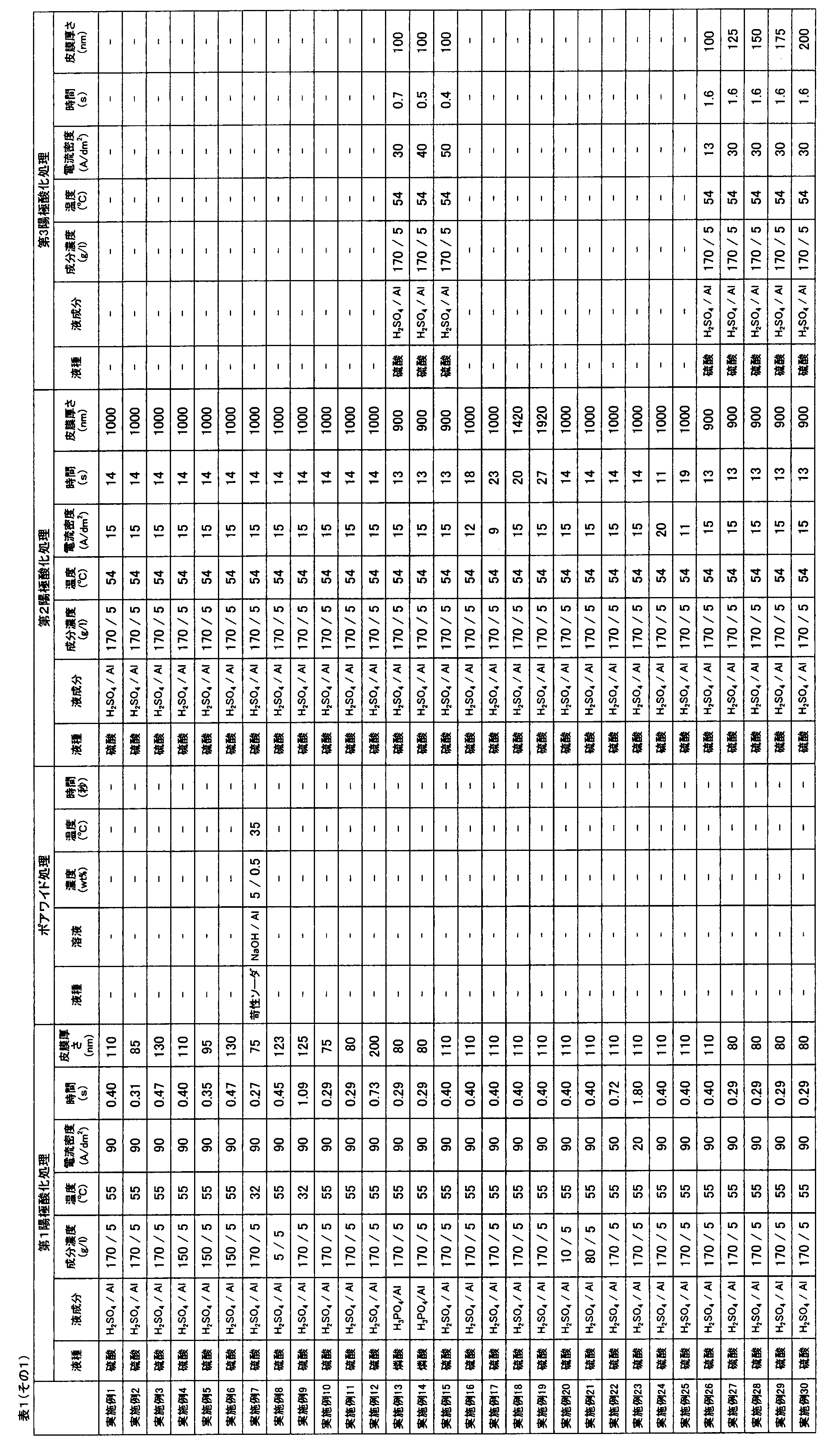
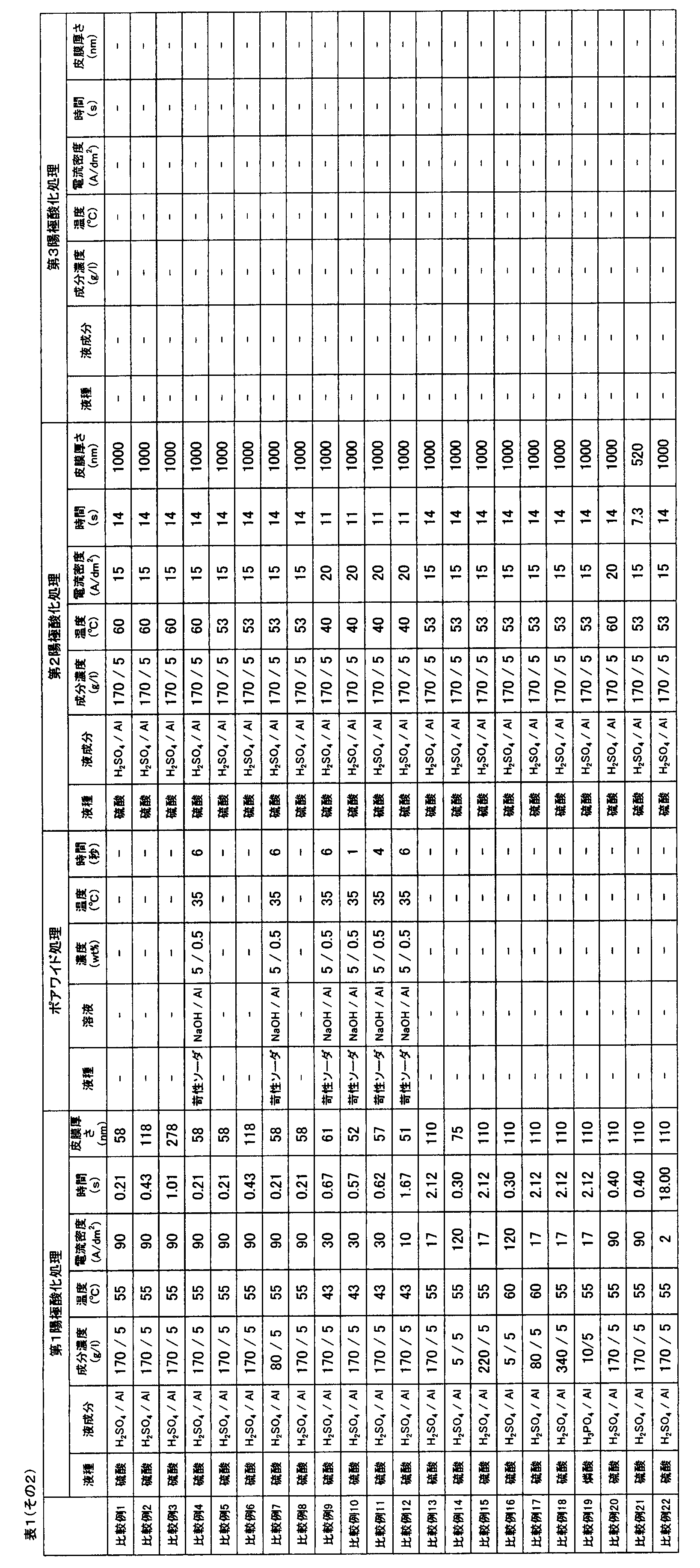

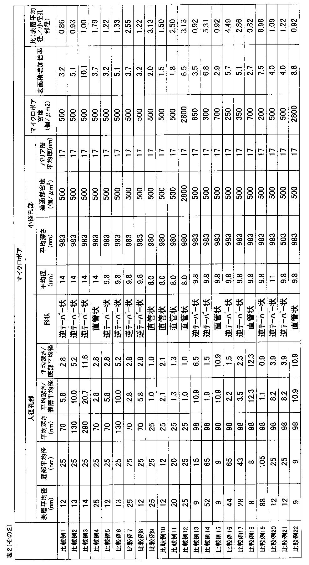
上記で製造した各平版印刷版用支持体に対し、下記下塗り液を乾燥塗布量が28mg/m2になるよう塗布して、下塗り層を設けた。
・下記構造の下塗り層用化合物(1) 0.18g
・ヒドロキシエチルイミノ二酢酸 0.10g
・メタノール 55.24g
・水 6.15g
全ての画像記録層塗布液は、各感光液およびミクロゲル液を塗布直前に混合し攪拌することにより得た。
・バインダーポリマー(1)〔下記構造〕 0.24g
・赤外線吸収剤(1)〔下記構造〕 0.030g
・ラジカル重合開始剤(1)〔下記構造〕 0.162g
・重合性化合物 トリス(アクリロイルオキシエチル)イソシアヌレート(NKエステルA-9300、新中村化学社製) 0.192g
・低分子親水性化合物トリス(2-ヒドロキシエチル)イソシアヌレート
0.062g
・低分子親水性化合物(1)〔下記構造〕 0.052g
・感脂化剤
ホスホニウム化合物(1)〔下記構造〕 0.055g
・感脂化剤
ベンジル-ジメチル-オクチルアンモニウム・PF6塩 0.018g
・ベタイン誘導体(C-1) 0.010g
・フッ素系界面活性剤(1)(平均重量分子量:1万)〔下記構造〕 0.008g
・メチルエチルケトン 1.091g
・1-メトキシ-2-プロパノール 8.609g
・ミクロゲル(1) 2.640g
・蒸留水 2.425g

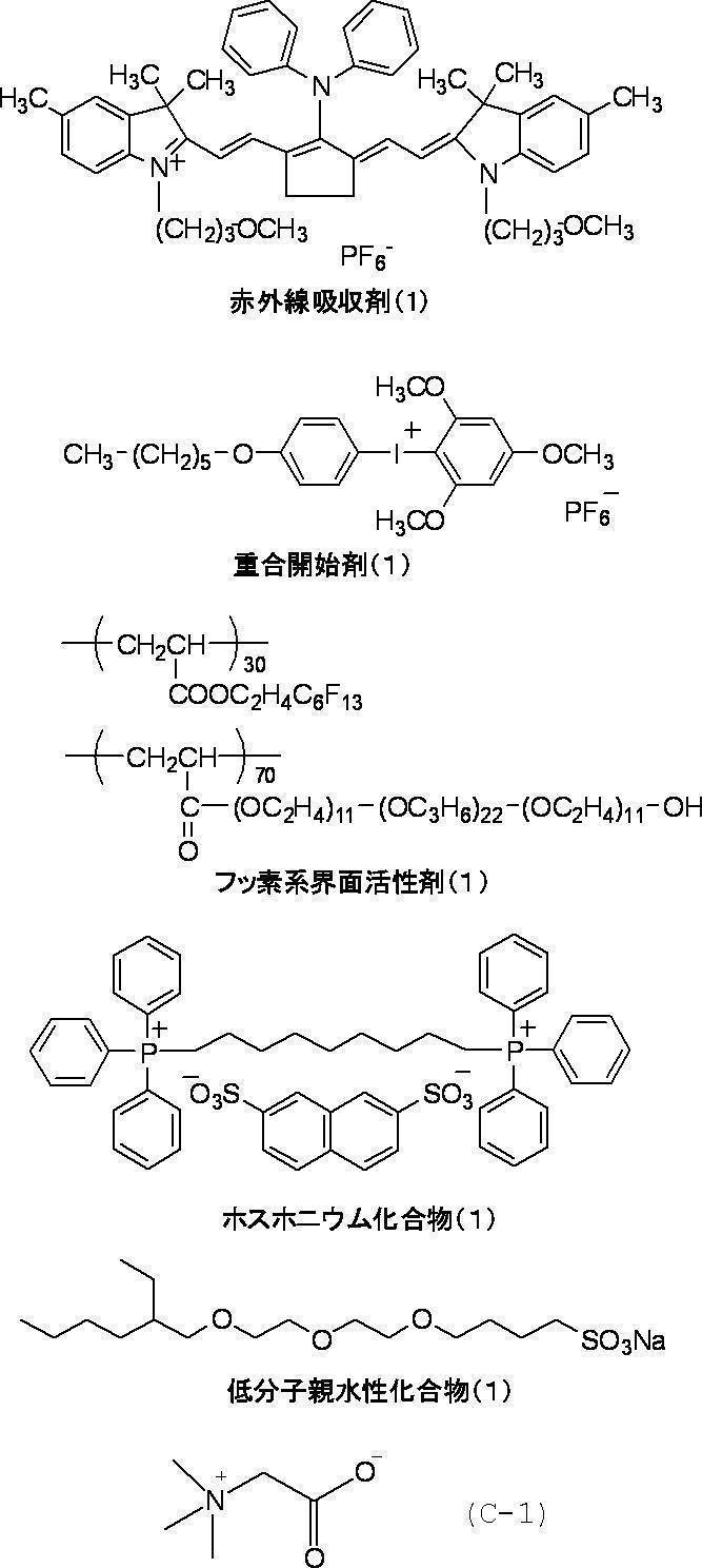
油相成分として、トリメチロールプロパンとキシレンジイソシアナート付加体(タケネートD-110N、三井武田ケミカル社製)10g、ペンタエリスリトールトリアクリレート(SR444、日本化薬社製)3.15g、およびパイオニンA-41C(竹本油脂社製)0.1gを酢酸エチル17gに溶解した。水相成分としてPVA-205の4質量%水溶液40gを調製した。油相成分および水相成分を混合し、ホモジナイザーを用いて12,000rpmで10分間乳化した。得られた乳化物を、蒸留水25gに添加し、室温で30分攪拌後、50℃で3時間攪拌した。このようにして得られたミクロゲル液の固形分濃度を、15質量%になるように蒸留水を用いて希釈し、これを上記ミクロゲル(1)とした。ミクロゲルの平均粒径を光散乱法により測定したところ、平均粒径は0.2μmであった。
・無機質層状化合物分散液(1) 1.5g
・ポリビニルアルコール(CKS50、スルホン酸変性、けん化度99モル%以上、重合度300、日本合成化学工業社製)6質量%水溶液 0.55g
・ポリビニルアルコール(PVA-405、けん化度81.5モル%、重合度500、クラレ社製)6質量%水溶液 0.03g
・界面活性剤(エマレックス710、日本エマルジョン社製)1質量%水溶液
8.60g
・イオン交換水 6.0g
イオン交換水193.6gに合成雲母ソマシフME-100(コープケミカル(株)製)6.4gを添加し、ホモジナイザーを用いて平均粒径(レーザー散乱法)が3μmになるまで分散した。得られた分散粒子のアスペクト比は100以上であった。
(機上現像性)
得られた平版印刷版原版を赤外線半導体レーザー搭載の富士フイルム(株)製Luxel PLATESETTER T-6000IIIにて、外面ドラム回転数1000rpm、レーザー出力70%、解像度2400dpiの条件で露光した。露光画像にはベタ画像および20μmドットFMスクリーンの50%網点チャートを含むようにした。
得られた露光済み原版を現像処理することなく、(株)小森コーポレーション製印刷機LITHRONE26の版胴に取り付けた。Ecolity-2(富士フイルム(株)製)/水道水=2/98(容量比)の湿し水とValues-G(N)墨インキ(大日本インキ化学工業(株)製)とを用い、LITHRONE26の標準自動印刷スタート方法で湿し水とインキとを供給して機上現像した後、毎時10000枚の印刷速度で、特菱アート(76.5kg)紙に印刷を100枚行った。
50%網点チャートの未露光部の印刷機上での機上現像が完了し、網点非画像部にインキが転写しない状態になるまでに要した印刷用紙の枚数を機上現像性として計測した。機上現像性のよい方から順に、A(損紙15枚以下)、B(損紙16~19枚以上)、C(損紙20~30枚)、D(損紙31枚以上)で表した。結果を表3に示す。
上記機上現像終了後、良好な印刷物が得られるようになった後に、印刷を一旦停止し、25℃、湿度50%の部屋において、印刷機上で1時間放置して、印刷を再開した時に、汚れのない良好な印刷物が得られるまでに要した印刷用紙の損紙枚数を評価した。放置払い性のよい方から順に、A(損紙75枚以下)、B(損紙76~300枚)、C(損紙301枚以上)で表した。結果を表3に示す。
上記同様の印刷機および手法で機上現像したのち、さらに印刷を続けた。ベタ画像の濃度が薄くなり始めたと目視で認められた時点の印刷枚数により、耐刷性を評価した。印刷枚数が3.0万枚未満のものをD、3.0万枚以上3.5万枚未満のものをC、3.5万枚以上3.75万枚未満のものをB、3.75万枚以上のものをAとした。結果を表3に示す。なお、表3中の評価結果としては、「D」または「C」が含まれていないことが必要である。
上記機上現像終了後、良好な印刷物が得られるようになった後に、ワニスを添加したFushion-EZ(S)インキ(大日本インキ化学工業(株)製)を平版印刷版の非画像部に塗り、印刷を再開した時に汚れのない良好な印刷物が得られるまでに要した印刷用紙の損紙枚数を評価した。インキ払い性のよい方から順に、A(損紙10枚以下)、B(損紙10枚超20枚以下)、C(損紙20枚超30枚以下)、D(損紙30枚超)で表した。結果を表3に示す。
平版印刷版用支持体の耐傷性は、得られた平版印刷版用支持体表面の引っ掻き試験により評価した。
引っ掻き試験は、連続加重式引っ掻き強度試験器(SB-53、新東科学社製)を用いて、サファイヤ針0.4mmφ、針の移動速度10cm/秒の条件下、加重100gで行った。
その結果、針によるキズがアルミニウム合金板(素地)の表面に達していないものを耐傷性に優れるものとして「A」と評価し、達しているものを「B」と評価した。なお、加重値が100gで耐傷性に優れる平版印刷版用支持体は、平版印刷版原版にしたときの巻き取り時および積層中における画像記録層へのキズの転写を抑制でき、非画像部の汚れを抑制することができる。なお、実用上、「A」であることが必要である。
得られた平版印刷版原版を、25℃、70%RHの環境下で1時間、合紙と共に調湿し、アルミクラフト紙で包装した後、60℃に設定したオーブンで10日間加熱を行った。
その後、室温まで温度を下げてから、上記同様の印刷機および手法で機上現像したのち、印刷を500枚行った。500枚目の印刷物を目視により確認し、80cm2当たりの、20μm以上の印刷汚れ(ポツ状汚れ)の個数を算出した。
ポツ状汚れが、200個以上のものを「E」、150個以上200個未満のものを「D」、100個以上150個未満のものを「C」、50個以上100個未満のものを「B」、30個以上50個未満のものを「A」、30個未満のものを「AA」とする。
なお、実用上、「E」でないことが好ましい。


なお、実施例1~6、8~22、24~30において得られたマイクロポアを構成する大径孔部の形状は、陽極酸化皮膜表面からアルミニウム板側に向かって径が大きくなる(表層平均径より底部平均径がより大きい)逆テーパー状(円錐状)であった。また、実施例7および23において得られたマイクロポアを構成する大径孔部の形状は、略直管状であった。
また、実施例1と2との比較より、大径孔部の平均深さが85~105nmであるとより優れた効果が得られることが確認された。
また、実施例1と5との比較より、大径孔部の平均径が11~13nmであるとより優れた効果が得られることが確認された。
特に、特許文献1の実施例1、2、3および16の態様に該当する比較例9~12においては、上記実施例1~30と比較して、耐刷性に劣る結果が得られた。
実施例13~15、実施例26~30においては、いずれも評価は「A」であり良好であった。
エッジ焼けは、EPMAにおいて、両エッジを含む幅方向の酸素強度を測定し、中心部の値に対し10%以上酸素強度が高い部分をエッジ焼け部とし、幅方向に対する長さを算出した。
その結果、エッジ焼けの幅方向の長さが5mm未満であるものを「A」、5mm以上であるものを「B」とする。
<平版印刷版原版の製造(その2)>
上記で製造した各平版印刷版用支持体(実施例1~3、5、16、比較例1~3、15)に対し、10秒間にわたり4g/lのポリビニルホスホン酸を含有する溶液で40℃において後処理し、脱塩水で20℃において2秒間にわたりすすぎそして乾燥した。
次いで、上記の基板上に、以下の画像記録層塗布液をバー塗布した後、50℃60秒でオーブン乾燥し、乾燥塗布量0.91g/m2の画像記録層を形成した。
SAN(スチレン/アクリロニトリル共重合体(モル比50/50)) 0.70g
赤外線吸収剤(2)〔下記構造〕 0.10g
PVA205(クラレ(株)製) 0.10g
メガファックF-177(大日本インキ化学工業(株)製 フッ素系界面活性剤)20質量%水溶液 0.05g


2、4 ローラ状ブラシ
3 研磨スラリー液
5、6、7、8 支持ローラ
ta アノード反応時間
tc カソード反応時間
tp 電流が0からピークに達するまでの時間
Ia アノードサイクル側のピーク時の電流
Ic カソードサイクル側のピーク時の電流
10,100 平版印刷版用支持体
12 アルミニウム板
14,14a,14b,14c 陽極酸化皮膜
16,16a,16b,16c マイクロポア
18,18a 大径孔部
20 小径孔部
50 主電解槽
51 交流電源
52 ラジアルドラムローラ
53a,53b 主極
54 電解液供給口
55 電解液
56 補助陽極
60 補助陽極槽
W アルミニウム板
610 陽極酸化処理装置
612 給電槽
614 電解処理槽
616 アルミニウム板
618、626 電解液
620 給電電極
622、628 ローラ
624 ニップローラ
630 電解電極
632 槽壁
634 直流電源
Claims (9)
- アルミニウム板と、その上にアルミニウムの陽極酸化皮膜とを備え、前記陽極酸化皮膜中に前記アルミニウム板とは反対側の表面から深さ方向にのびるマイクロポアを有する平版印刷版用支持体であって、
前記マイクロポアが、前記陽極酸化皮膜表面から平均深さ75~120nm(深さA)の位置までのびる大径孔部と、前記大径孔部の底部と連通し、連通位置から平均深さ900~2000nmの位置までのびる小径孔部とから構成され、
前記大径孔部の前記陽極酸化皮膜表面における平均径が10nm以上30nm未満で、前記大径孔部の前記平均径と深さAとが(深さA/平均径)=4.0超12.0以下の関係を満たし、
前記小径孔部の前記連通位置における平均径が0より大きく10.0nm未満である平版印刷版用支持体。 - 前記小径孔部が、平均深さが異なる第1の小径孔部と第2の小径孔部とを有し、
前記第1の小径孔部の平均深さが前記第2の小径孔部の平均深さよりも深く、
前記第1の小径孔部の底部から前記アルミニウム板表面までの陽極酸化皮膜の平均厚みが17nm以上であり、最少厚みが15nm以上である、請求項1に記載の平版印刷板用支持体。 - 前記第1の小径孔部の密度が550~700個/μm2である、請求項1または2に記載の平版印刷版板用支持体。
- 前記第1の小径孔部の平均深さと、前記第2の小径孔部の平均深さとの差が、75~200nmである、請求項1~3のいずれか1項に記載の平版印刷版用支持体。
- 前記大径孔部の径が前記陽極酸化皮膜表面から前記アルミニウム板側に向かって漸増して、前記大径孔部の前記陽極酸化皮膜表面における平均径(表層平均径)より前記連通位置における大径孔部の平均径(底部平均径)が大きく、前記底部平均径が10nm超60nm以下であり、前記底部平均径と深さAとの比(深さA/底部平均径)が1.2以上12.0未満である、請求項1~4のいずれか1項に記載の平版印刷版用支持体。
- 前記大径孔部の下記式(A)に示す表面積増加倍率が1.9~16.0である、請求項5に記載の平版印刷版用支持体。
式(A):(表面積増加倍率)=1+ポア密度×((π×(表層平均径/2+底部平均径/2)×((底部平均径/2-表層平均径/2)2+深さA2)1/2+π×(底部平均径/2)2-π×(表層平均径/2)2)) - 前記大径孔部の陽極酸化皮膜表面における平均径と、前記小径孔部の前記連通位置における平均径との比(大径孔部の平均径/小径孔部の平均径)が1.00超1.50以下である、請求項1~6のいずれか1項に記載の平版印刷版用支持体。
- 請求項1~7のいずれか1項に記載の平版印刷版用支持体上に、画像記録層を有することを特徴とする平版印刷版原版。
- アルミニウム板を陽極酸化する第1陽極酸化処理工程と、
前記第1陽極酸化処理工程で得られた陽極酸化皮膜を有するアルミニウム板を、さらに陽極酸化する第2陽極酸化処理工程とを備え、請求項1~7のいずれか1項に記載の平版印刷版用支持体を製造する、平版印刷版用支持体の製造方法。
Priority Applications (4)
| Application Number | Priority Date | Filing Date | Title |
|---|---|---|---|
| BR112015001857-2A BR112015001857B1 (pt) | 2012-07-27 | 2013-07-26 | Suporte para chapa de impressão litográfica, precursor da chapa de impressão litográfica e método de produção do suporte para chapa de impressão litográfica |
| CN201380039683.5A CN104487261B (zh) | 2012-07-27 | 2013-07-26 | 平版印刷版用支撑体及其制造方法、以及平版印刷版原版 |
| EP13823769.8A EP2878452B1 (en) | 2012-07-27 | 2013-07-26 | Support for lithographic printing plate and manufacturing method therefor |
| US14/603,600 US9259954B2 (en) | 2012-07-27 | 2015-01-23 | Support for lithographic printing plate and manufacturing method therefor, as well as original lithographic printing plate |
Applications Claiming Priority (6)
| Application Number | Priority Date | Filing Date | Title |
|---|---|---|---|
| JP2012167777 | 2012-07-27 | ||
| JP2012-167777 | 2012-07-27 | ||
| JP2012-210628 | 2012-09-25 | ||
| JP2012210628 | 2012-09-25 | ||
| JP2013-054293 | 2013-03-15 | ||
| JP2013054293 | 2013-03-15 |
Related Child Applications (1)
| Application Number | Title | Priority Date | Filing Date |
|---|---|---|---|
| US14/603,600 Continuation US9259954B2 (en) | 2012-07-27 | 2015-01-23 | Support for lithographic printing plate and manufacturing method therefor, as well as original lithographic printing plate |
Publications (1)
| Publication Number | Publication Date |
|---|---|
| WO2014017640A1 true WO2014017640A1 (ja) | 2014-01-30 |
Family
ID=49997444
Family Applications (1)
| Application Number | Title | Priority Date | Filing Date |
|---|---|---|---|
| PCT/JP2013/070348 Ceased WO2014017640A1 (ja) | 2012-07-27 | 2013-07-26 | 平版印刷版用支持体およびその製造方法、並びに、平版印刷版原版 |
Country Status (6)
| Country | Link |
|---|---|
| US (1) | US9259954B2 (ja) |
| EP (1) | EP2878452B1 (ja) |
| JP (1) | JP5813063B2 (ja) |
| CN (1) | CN104487261B (ja) |
| BR (1) | BR112015001857B1 (ja) |
| WO (1) | WO2014017640A1 (ja) |
Cited By (5)
| Publication number | Priority date | Publication date | Assignee | Title |
|---|---|---|---|---|
| WO2015122513A1 (ja) * | 2014-02-17 | 2015-08-20 | 富士フイルム株式会社 | 平版印刷版の基準マーク検出方法、平版印刷版の加工方法、及び、印刷方法 |
| WO2019064694A1 (ja) * | 2017-09-29 | 2019-04-04 | 富士フイルム株式会社 | 印刷版原版、印刷版の製造方法、印刷方法 |
| WO2020162785A1 (ru) * | 2019-02-07 | 2020-08-13 | Сергей Геннадьевич КАПЛУНОВ | Способ воспроизведения авторских рисунков на металлографской доске |
| WO2020162784A1 (ru) * | 2019-02-07 | 2020-08-13 | Сергей Геннадьевич КАПЛУНОВ | Способ изготовления печатной формы для офорта и травильный раствор для его осуществления |
| CN113089047A (zh) * | 2021-04-12 | 2021-07-09 | 四川九洲电器集团有限责任公司 | 一种铝合金构件及其制备方法、应用 |
Families Citing this family (21)
| Publication number | Priority date | Publication date | Assignee | Title |
|---|---|---|---|---|
| JP6486741B2 (ja) * | 2015-03-24 | 2019-03-20 | 富士フイルム株式会社 | 平版印刷版原版、平版印刷版の製版方法、及び、印刷方法 |
| WO2017168831A1 (ja) * | 2016-03-30 | 2017-10-05 | 富士フイルム株式会社 | 機上現像用平版印刷版原版、平版印刷版の作製方法、及び、平版印刷方法 |
| CN109153278B (zh) * | 2016-05-30 | 2020-06-05 | 富士胶片株式会社 | 平版印刷版用铝支撑体及平版印刷版原版 |
| US10363734B2 (en) | 2017-03-02 | 2019-07-30 | Eastman Kodak Company | Method for making lithographic printing plates |
| US10828884B2 (en) * | 2017-03-02 | 2020-11-10 | Eastman Kodak Company | Lithographic printing plate precursors and method of use |
| CN111361324B (zh) * | 2017-03-31 | 2021-10-19 | 富士胶片株式会社 | 平版印刷版原版、其制造方法、其层叠体、平版印刷方法 |
| JP6454058B1 (ja) * | 2017-03-31 | 2019-01-16 | 富士フイルム株式会社 | 平版印刷版原版及びその製造方法、平版印刷版原版積層体、平版印刷版の製版方法、並びに、平版印刷方法 |
| WO2019044702A1 (ja) * | 2017-08-31 | 2019-03-07 | 富士フイルム株式会社 | 平版印刷版原版 |
| WO2019044431A1 (ja) * | 2017-08-31 | 2019-03-07 | 富士フイルム株式会社 | 平版印刷版の作製方法 |
| CN109729714B (zh) | 2017-08-31 | 2021-06-18 | 富士胶片株式会社 | 平版印刷版原版、平版印刷版的制造方法、印刷方法 |
| WO2019064696A1 (ja) * | 2017-09-29 | 2019-04-04 | 富士フイルム株式会社 | 平版印刷版原版、平版印刷版の作製方法及び平版印刷方法 |
| WO2019150998A1 (ja) * | 2018-01-31 | 2019-08-08 | 富士フイルム株式会社 | ポジ型平版印刷版原版及び平版印刷版の作製方法 |
| CN111867848B (zh) * | 2018-03-28 | 2021-10-15 | 富士胶片株式会社 | 平版印刷版原版及平版印刷版原版的制造方法 |
| WO2020262694A1 (ja) * | 2019-06-28 | 2020-12-30 | 富士フイルム株式会社 | 平版印刷版原版、平版印刷版の作製方法、及び平版印刷方法 |
| US11117412B2 (en) | 2019-10-01 | 2021-09-14 | Eastman Kodak Company | Lithographic printing plate precursors and method of use |
| CN119821020A (zh) | 2019-12-27 | 2025-04-15 | 富士胶片株式会社 | 平版印刷版原版、平版印刷版的制造方法及印刷方法 |
| US11964466B2 (en) * | 2020-10-21 | 2024-04-23 | Eastman Kodak Company | Lithographic printing plate precursors and method of use |
| JP2023553000A (ja) | 2020-12-04 | 2023-12-20 | イーストマン コダック カンパニー | 平版印刷版原版および使用方法 |
| JP2023554644A (ja) | 2020-12-17 | 2023-12-28 | イーストマン コダック カンパニー | 平版印刷版原版および使用方法 |
| US11813884B2 (en) | 2020-12-17 | 2023-11-14 | Eastman Kodak Company | Lithographic printing plate precursors and method of use |
| US12429774B2 (en) | 2022-08-04 | 2025-09-30 | Eastman Kodak Company | Lithographic printing plate precursors, methods of using and manufacture |
Citations (34)
| Publication number | Priority date | Publication date | Assignee | Title |
|---|---|---|---|---|
| US2714066A (en) | 1950-12-06 | 1955-07-26 | Minnesota Mining & Mfg | Planographic printing plate |
| US3181461A (en) | 1963-05-23 | 1965-05-04 | Howard A Fromson | Photographic plate |
| GB1084070A (en) | 1960-08-05 | 1967-09-20 | Kalle Ag | Process and material for the preparation of planographic printing plates |
| US3458311A (en) | 1966-06-27 | 1969-07-29 | Du Pont | Photopolymerizable elements with solvent removable protective layers |
| JPS4841708B1 (ja) | 1970-01-13 | 1973-12-07 | ||
| GB1412768A (en) | 1971-10-07 | 1975-11-05 | Fuji Photo Film Co Ltd | Process for producing a base plate for a photosensitive printing plate |
| JPS5040047B2 (ja) | 1971-09-06 | 1975-12-22 | ||
| JPS5549729B2 (ja) | 1973-02-07 | 1980-12-13 | ||
| US4458005A (en) | 1981-07-06 | 1984-07-03 | Hoechst Aktiengesellschaft | Polyvinylmethylphosphinic acid, process for its manufacture and use |
| JPS62170950A (ja) | 1986-01-23 | 1987-07-28 | Fuji Photo Film Co Ltd | 感光性組成物 |
| EP0291760A2 (de) | 1987-05-12 | 1988-11-23 | Hoechst Aktiengesellschaft | Druckplattenträger sowie Verfahren und Vorrichtung zu dessen Herstellung |
| EP0292801A2 (de) | 1987-05-26 | 1988-11-30 | Hoechst Aktiengesellschaft | Verfahren zur elektrochemischen Aufrauhung von Aluminium für Druckplattenträger |
| EP0400706A1 (en) | 1989-05-31 | 1990-12-05 | Agfa-Gevaert N.V. | Dyes and dye-donor elements for use in thermal dye sublimation transfer |
| DE4001466A1 (de) | 1990-01-19 | 1991-07-25 | Hoechst Ag | Verfahren zur elektrochemischen aufrauhung von aluminium fuer druckplattentraeger |
| EP0537633A1 (de) | 1991-10-16 | 1993-04-21 | Hoechst Aktiengesellschaft | Verfahren zur Behandlung von aufgerauhten und anodisierten Flachdruckplatten und danach hergestellte Flachdruckplatten |
| JPH05195300A (ja) | 1992-01-23 | 1993-08-03 | Fuji Photo Film Co Ltd | 電解処理装置 |
| EP0659909A1 (en) | 1993-12-22 | 1995-06-28 | Hoechst Aktiengesellschaft | Electrochemical graining method |
| DE4417907A1 (de) | 1994-05-21 | 1995-11-23 | Hoechst Ag | Verfahren zur Nachbehandlung von platten-, folien- oder bandförmigem Material, Träger aus derartigem Material und seine Verwendung für Offsetdruckplatten |
| DE4423140A1 (de) | 1994-07-01 | 1996-01-04 | Hoechst Ag | Hydrophiliertes Trägermaterial und damit hergestelltes Aufzeichnungsmaterial |
| JPH0818327B2 (ja) | 1992-03-02 | 1996-02-28 | ラサ工業株式会社 | コアドリル |
| WO1997039894A1 (en) | 1996-04-23 | 1997-10-30 | Horsell Graphic Industries Limited | Heat-sensitive composition and method of making a lithographic printing form with it |
| EP0823327A2 (en) | 1996-08-06 | 1998-02-11 | Mitsubishi Chemical Corporation | Positive photosensitive composition, positive photosensitive lithographic printing plate and method for making positive photosensitive lithographic printing plate |
| EP0978376A2 (de) | 1998-08-01 | 2000-02-09 | Agfa-Gevaert AG | Strahlungsempfindlisches Gemisch mit IR-absorbierenden, betainischen oder betainisch-anionischen Cyaninfarbstoffen und damit hergestelltes Aufzeichnungsmaterial |
| WO2000029214A1 (en) | 1998-11-16 | 2000-05-25 | Mitsubishi Chemical Corporation | Positive-working photosensitive lithographic printing plate and method for producing the same |
| EP1029667A1 (en) | 1999-02-15 | 2000-08-23 | Fuji Photo Film Co., Ltd. | Positive planographic printing material |
| EP1053868A2 (en) | 1999-05-21 | 2000-11-22 | Fuji Photo Film Co., Ltd. | Photosensitive composition and planographic printing plate base using same |
| EP1093934A1 (en) | 1999-10-19 | 2001-04-25 | Fuji Photo Film Co., Ltd. | Photosensitive composition and planographic printing plate using the same |
| EP1219416A1 (en) | 2000-12-20 | 2002-07-03 | Agfa-Gevaert | On-press development printing method using a negative working thermally sensitive lithographic printing plate |
| JP2003001956A (ja) | 2001-03-15 | 2003-01-08 | Fuji Photo Film Co Ltd | 平版印刷版用支持体および平版印刷版原版 |
| JP2005254638A (ja) | 2004-03-12 | 2005-09-22 | Fuji Photo Film Co Ltd | 平版印刷版用支持体の製造方法 |
| JP2009255434A (ja) | 2008-04-18 | 2009-11-05 | Fujifilm Corp | 平版印刷版用アルミニウム合金板、平版印刷版用支持体、平版印刷版用原版および平版印刷版用アルミニウム合金板の製造方法 |
| JP2011173413A (ja) * | 2010-01-29 | 2011-09-08 | Fujifilm Corp | 平版印刷版用支持体、平版印刷版用支持体の製造方法、および平版印刷版原版 |
| JP2011245844A (ja) | 2009-12-28 | 2011-12-08 | Fujifilm Corp | 平版印刷版用支持体、平版印刷版用支持体の製造方法、および平版印刷版原版 |
| JP2012071435A (ja) * | 2010-09-28 | 2012-04-12 | Fujifilm Corp | 平版印刷版用支持体、平版印刷版用支持体の製造方法、および平版印刷版原版 |
Family Cites Families (6)
| Publication number | Priority date | Publication date | Assignee | Title |
|---|---|---|---|---|
| JP3787334B2 (ja) * | 2002-12-27 | 2006-06-21 | 富士写真フイルム株式会社 | 平版印刷版原版 |
| JP2009078366A (ja) * | 2007-09-25 | 2009-04-16 | Fujifilm Corp | 平版印刷版原版、及びその製造方法 |
| CN102301040B (zh) * | 2009-01-30 | 2014-10-15 | 夏普株式会社 | 模具和模具的制造方法、以及使用模具的防反射膜的制造方法 |
| JP5612531B2 (ja) * | 2010-04-30 | 2014-10-22 | 富士フイルム株式会社 | 平版印刷版用支持体、および平版印刷版原版 |
| JP2012187909A (ja) * | 2010-07-23 | 2012-10-04 | Fujifilm Corp | 平版印刷版用支持体、および、平版印刷版原版 |
| CN102381072B (zh) * | 2010-08-27 | 2016-02-24 | 富士胶片株式会社 | 平版印刷版用铝支撑体的制造方法及制造装置 |
-
2013
- 2013-07-26 EP EP13823769.8A patent/EP2878452B1/en active Active
- 2013-07-26 WO PCT/JP2013/070348 patent/WO2014017640A1/ja not_active Ceased
- 2013-07-26 BR BR112015001857-2A patent/BR112015001857B1/pt active IP Right Grant
- 2013-07-26 JP JP2013155477A patent/JP5813063B2/ja active Active
- 2013-07-26 CN CN201380039683.5A patent/CN104487261B/zh active Active
-
2015
- 2015-01-23 US US14/603,600 patent/US9259954B2/en active Active
Patent Citations (34)
| Publication number | Priority date | Publication date | Assignee | Title |
|---|---|---|---|---|
| US2714066A (en) | 1950-12-06 | 1955-07-26 | Minnesota Mining & Mfg | Planographic printing plate |
| GB1084070A (en) | 1960-08-05 | 1967-09-20 | Kalle Ag | Process and material for the preparation of planographic printing plates |
| US3181461A (en) | 1963-05-23 | 1965-05-04 | Howard A Fromson | Photographic plate |
| US3458311A (en) | 1966-06-27 | 1969-07-29 | Du Pont | Photopolymerizable elements with solvent removable protective layers |
| JPS4841708B1 (ja) | 1970-01-13 | 1973-12-07 | ||
| JPS5040047B2 (ja) | 1971-09-06 | 1975-12-22 | ||
| GB1412768A (en) | 1971-10-07 | 1975-11-05 | Fuji Photo Film Co Ltd | Process for producing a base plate for a photosensitive printing plate |
| JPS5549729B2 (ja) | 1973-02-07 | 1980-12-13 | ||
| US4458005A (en) | 1981-07-06 | 1984-07-03 | Hoechst Aktiengesellschaft | Polyvinylmethylphosphinic acid, process for its manufacture and use |
| JPS62170950A (ja) | 1986-01-23 | 1987-07-28 | Fuji Photo Film Co Ltd | 感光性組成物 |
| EP0291760A2 (de) | 1987-05-12 | 1988-11-23 | Hoechst Aktiengesellschaft | Druckplattenträger sowie Verfahren und Vorrichtung zu dessen Herstellung |
| EP0292801A2 (de) | 1987-05-26 | 1988-11-30 | Hoechst Aktiengesellschaft | Verfahren zur elektrochemischen Aufrauhung von Aluminium für Druckplattenträger |
| EP0400706A1 (en) | 1989-05-31 | 1990-12-05 | Agfa-Gevaert N.V. | Dyes and dye-donor elements for use in thermal dye sublimation transfer |
| DE4001466A1 (de) | 1990-01-19 | 1991-07-25 | Hoechst Ag | Verfahren zur elektrochemischen aufrauhung von aluminium fuer druckplattentraeger |
| EP0537633A1 (de) | 1991-10-16 | 1993-04-21 | Hoechst Aktiengesellschaft | Verfahren zur Behandlung von aufgerauhten und anodisierten Flachdruckplatten und danach hergestellte Flachdruckplatten |
| JPH05195300A (ja) | 1992-01-23 | 1993-08-03 | Fuji Photo Film Co Ltd | 電解処理装置 |
| JPH0818327B2 (ja) | 1992-03-02 | 1996-02-28 | ラサ工業株式会社 | コアドリル |
| EP0659909A1 (en) | 1993-12-22 | 1995-06-28 | Hoechst Aktiengesellschaft | Electrochemical graining method |
| DE4417907A1 (de) | 1994-05-21 | 1995-11-23 | Hoechst Ag | Verfahren zur Nachbehandlung von platten-, folien- oder bandförmigem Material, Träger aus derartigem Material und seine Verwendung für Offsetdruckplatten |
| DE4423140A1 (de) | 1994-07-01 | 1996-01-04 | Hoechst Ag | Hydrophiliertes Trägermaterial und damit hergestelltes Aufzeichnungsmaterial |
| WO1997039894A1 (en) | 1996-04-23 | 1997-10-30 | Horsell Graphic Industries Limited | Heat-sensitive composition and method of making a lithographic printing form with it |
| EP0823327A2 (en) | 1996-08-06 | 1998-02-11 | Mitsubishi Chemical Corporation | Positive photosensitive composition, positive photosensitive lithographic printing plate and method for making positive photosensitive lithographic printing plate |
| EP0978376A2 (de) | 1998-08-01 | 2000-02-09 | Agfa-Gevaert AG | Strahlungsempfindlisches Gemisch mit IR-absorbierenden, betainischen oder betainisch-anionischen Cyaninfarbstoffen und damit hergestelltes Aufzeichnungsmaterial |
| WO2000029214A1 (en) | 1998-11-16 | 2000-05-25 | Mitsubishi Chemical Corporation | Positive-working photosensitive lithographic printing plate and method for producing the same |
| EP1029667A1 (en) | 1999-02-15 | 2000-08-23 | Fuji Photo Film Co., Ltd. | Positive planographic printing material |
| EP1053868A2 (en) | 1999-05-21 | 2000-11-22 | Fuji Photo Film Co., Ltd. | Photosensitive composition and planographic printing plate base using same |
| EP1093934A1 (en) | 1999-10-19 | 2001-04-25 | Fuji Photo Film Co., Ltd. | Photosensitive composition and planographic printing plate using the same |
| EP1219416A1 (en) | 2000-12-20 | 2002-07-03 | Agfa-Gevaert | On-press development printing method using a negative working thermally sensitive lithographic printing plate |
| JP2003001956A (ja) | 2001-03-15 | 2003-01-08 | Fuji Photo Film Co Ltd | 平版印刷版用支持体および平版印刷版原版 |
| JP2005254638A (ja) | 2004-03-12 | 2005-09-22 | Fuji Photo Film Co Ltd | 平版印刷版用支持体の製造方法 |
| JP2009255434A (ja) | 2008-04-18 | 2009-11-05 | Fujifilm Corp | 平版印刷版用アルミニウム合金板、平版印刷版用支持体、平版印刷版用原版および平版印刷版用アルミニウム合金板の製造方法 |
| JP2011245844A (ja) | 2009-12-28 | 2011-12-08 | Fujifilm Corp | 平版印刷版用支持体、平版印刷版用支持体の製造方法、および平版印刷版原版 |
| JP2011173413A (ja) * | 2010-01-29 | 2011-09-08 | Fujifilm Corp | 平版印刷版用支持体、平版印刷版用支持体の製造方法、および平版印刷版原版 |
| JP2012071435A (ja) * | 2010-09-28 | 2012-04-12 | Fujifilm Corp | 平版印刷版用支持体、平版印刷版用支持体の製造方法、および平版印刷版原版 |
Non-Patent Citations (3)
| Title |
|---|
| "Senryo Binran", 1970, THE SOCIETY OF SYNTHETIC ORGANIC CHEMISTRY |
| PARTICULATE SCIENCE AND TECHNOLOGY, vol. 7, 1989, pages 223 - 228 |
| STANLEY D. DUKE ET AL.: "Calibration of Spherical Particles by Light Scattering", TECHNICAL NOTE-002B, 3 January 2000 (2000-01-03) |
Cited By (6)
| Publication number | Priority date | Publication date | Assignee | Title |
|---|---|---|---|---|
| WO2015122513A1 (ja) * | 2014-02-17 | 2015-08-20 | 富士フイルム株式会社 | 平版印刷版の基準マーク検出方法、平版印刷版の加工方法、及び、印刷方法 |
| WO2019064694A1 (ja) * | 2017-09-29 | 2019-04-04 | 富士フイルム株式会社 | 印刷版原版、印刷版の製造方法、印刷方法 |
| JPWO2019064694A1 (ja) * | 2017-09-29 | 2020-07-02 | 富士フイルム株式会社 | 印刷版原版、印刷版の製造方法、印刷方法 |
| WO2020162785A1 (ru) * | 2019-02-07 | 2020-08-13 | Сергей Геннадьевич КАПЛУНОВ | Способ воспроизведения авторских рисунков на металлографской доске |
| WO2020162784A1 (ru) * | 2019-02-07 | 2020-08-13 | Сергей Геннадьевич КАПЛУНОВ | Способ изготовления печатной формы для офорта и травильный раствор для его осуществления |
| CN113089047A (zh) * | 2021-04-12 | 2021-07-09 | 四川九洲电器集团有限责任公司 | 一种铝合金构件及其制备方法、应用 |
Also Published As
| Publication number | Publication date |
|---|---|
| BR112015001857A2 (ja) | 2019-12-31 |
| US9259954B2 (en) | 2016-02-16 |
| JP2014198453A (ja) | 2014-10-23 |
| EP2878452A1 (en) | 2015-06-03 |
| EP2878452A4 (en) | 2016-03-23 |
| JP5813063B2 (ja) | 2015-11-17 |
| US20150135979A1 (en) | 2015-05-21 |
| CN104487261B (zh) | 2016-08-24 |
| CN104487261A (zh) | 2015-04-01 |
| EP2878452B1 (en) | 2018-11-28 |
| BR112015001857B1 (pt) | 2021-09-14 |
Similar Documents
| Publication | Publication Date | Title |
|---|---|---|
| JP5813063B2 (ja) | 平版印刷版用支持体およびその製造方法、並びに、平版印刷版原版 | |
| JP5498371B2 (ja) | 平版印刷版用支持体、平版印刷版用支持体の製造方法、および平版印刷版原版 | |
| JP5205480B2 (ja) | 平版印刷版用支持体、および平版印刷版原版 | |
| JP5498403B2 (ja) | 平版印刷版用支持体、平版印刷版用支持体の製造方法、および平版印刷版原版 | |
| JP6454828B1 (ja) | 平版印刷版原版、平版印刷版の製造方法、印刷方法 | |
| JP5612531B2 (ja) | 平版印刷版用支持体、および平版印刷版原版 | |
| CN102616049B (zh) | 平版印刷版载体和预制感光版 | |
| WO2013111652A1 (ja) | 平版印刷版用支持体、平版印刷版用支持体の製造方法、および平版印刷版原版 | |
| WO2019087516A1 (ja) | 平版印刷版原版、平版印刷版の製造方法、印刷方法およびアルミニウム支持体の製造方法 | |
| JP2015189021A (ja) | 平版印刷版用支持体およびその製造方法、並びに、平版印刷版原版 | |
| JP5498905B2 (ja) | 平版印刷版用支持体、平版印刷版用支持体の製造方法、および平版印刷版原版 | |
| JP5203477B2 (ja) | 平版印刷版用支持体、および平版印刷版原版 | |
| JP2005265501A (ja) | 水溶液中のフッ素化合物およびリン酸化合物の濃度測定方法 | |
| JP6639662B2 (ja) | 平版印刷版用アルミニウム支持体および平版印刷版原版 | |
| JPWO2019064694A1 (ja) | 印刷版原版、印刷版の製造方法、印刷方法 | |
| JP2005231348A (ja) | 印刷版材料、その現像方法及び印刷版材料用支持体 |
Legal Events
| Date | Code | Title | Description |
|---|---|---|---|
| 121 | Ep: the epo has been informed by wipo that ep was designated in this application |
Ref document number: 13823769 Country of ref document: EP Kind code of ref document: A1 |
|
| WWE | Wipo information: entry into national phase |
Ref document number: 2013823769 Country of ref document: EP |
|
| NENP | Non-entry into the national phase |
Ref country code: DE |
|
| REG | Reference to national code |
Ref country code: BR Ref legal event code: B01A Ref document number: 112015001857 Country of ref document: BR |
|
| ENP | Entry into the national phase |
Ref document number: 112015001857 Country of ref document: BR Kind code of ref document: A2 Effective date: 20150127 |
|
| REG | Reference to national code |
Ref country code: BR Ref legal event code: B01E Ref document number: 112015001857 Country of ref document: BR Kind code of ref document: A2 Free format text: APRESENTE A TRADUCAO SIMPLES DA FOLHA DE ROSTO DA CERTIDAO DE DEPOSITO DAS PRIORIDADES: JP 2012-167777, JP 2012-210628 E JP 2013-054293; OU DECLARACAO DE QUE OS DADOS DO PEDIDO INTERNACIONAL ESTAO FIELMENTE CONTIDOS NA PRIORIDADE REIVINDICADA, CONTENDO TODOS OS DADOS IDENTIFICADORES DESTA (TITULARES, NUMERO DE REGISTRO, DATA E TITULO), CONFORME O PARAGRAFO UNICO DO ART. 25 DA RESOLUCAO 77/2013. CABE SALIENTAR QUE NAO FOI POSSIVEL IDENTIFICAR OS TITULARES DO PEDIDO PRIORITARIO NOS DOCUMENTOS JUNTADOS AO PROCESSO, TAMPOUCO NOS APRESENTADOS NA OMPI, POIS SE ENCONTRAM EM JAPONES. |
|
| ENP | Entry into the national phase |
Ref document number: 112015001857 Country of ref document: BR Kind code of ref document: A2 Effective date: 20150127 |