WO2014017813A1 - 안테나 장치 - Google Patents
안테나 장치 Download PDFInfo
- Publication number
- WO2014017813A1 WO2014017813A1 PCT/KR2013/006601 KR2013006601W WO2014017813A1 WO 2014017813 A1 WO2014017813 A1 WO 2014017813A1 KR 2013006601 W KR2013006601 W KR 2013006601W WO 2014017813 A1 WO2014017813 A1 WO 2014017813A1
- Authority
- WO
- WIPO (PCT)
- Prior art keywords
- antenna element
- plate
- ground
- antenna
- frequency band
- Prior art date
- Legal status (The legal status is an assumption and is not a legal conclusion. Google has not performed a legal analysis and makes no representation as to the accuracy of the status listed.)
- Ceased
Links
Images


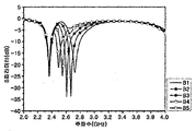

Classifications
-
- H—ELECTRICITY
- H01—ELECTRIC ELEMENTS
- H01Q—ANTENNAS, i.e. RADIO AERIALS
- H01Q1/00—Details of, or arrangements associated with, antennas
- H01Q1/52—Means for reducing coupling between antennas; Means for reducing coupling between an antenna and another structure
- H01Q1/521—Means for reducing coupling between antennas; Means for reducing coupling between an antenna and another structure reducing the coupling between adjacent antennas
- H01Q1/523—Means for reducing coupling between antennas; Means for reducing coupling between an antenna and another structure reducing the coupling between adjacent antennas between antennas of an array
-
- H—ELECTRICITY
- H01—ELECTRIC ELEMENTS
- H01Q—ANTENNAS, i.e. RADIO AERIALS
- H01Q9/00—Electrically-short antennas having dimensions not more than twice the operating wavelength and consisting of conductive active radiating elements
- H01Q9/04—Resonant antennas
-
- H—ELECTRICITY
- H01—ELECTRIC ELEMENTS
- H01Q—ANTENNAS, i.e. RADIO AERIALS
- H01Q1/00—Details of, or arrangements associated with, antennas
- H01Q1/12—Supports; Mounting means
- H01Q1/22—Supports; Mounting means by structural association with other equipment or articles
- H01Q1/24—Supports; Mounting means by structural association with other equipment or articles with receiving set
-
- H—ELECTRICITY
- H01—ELECTRIC ELEMENTS
- H01Q—ANTENNAS, i.e. RADIO AERIALS
- H01Q1/00—Details of, or arrangements associated with, antennas
- H01Q1/12—Supports; Mounting means
- H01Q1/22—Supports; Mounting means by structural association with other equipment or articles
- H01Q1/24—Supports; Mounting means by structural association with other equipment or articles with receiving set
- H01Q1/241—Supports; Mounting means by structural association with other equipment or articles with receiving set used in mobile communications, e.g. GSM
- H01Q1/242—Supports; Mounting means by structural association with other equipment or articles with receiving set used in mobile communications, e.g. GSM specially adapted for hand-held use
- H01Q1/243—Supports; Mounting means by structural association with other equipment or articles with receiving set used in mobile communications, e.g. GSM specially adapted for hand-held use with built-in antennas
-
- H—ELECTRICITY
- H01—ELECTRIC ELEMENTS
- H01Q—ANTENNAS, i.e. RADIO AERIALS
- H01Q1/00—Details of, or arrangements associated with, antennas
- H01Q1/36—Structural form of radiating elements, e.g. cone, spiral, umbrella; Particular materials used therewith
- H01Q1/38—Structural form of radiating elements, e.g. cone, spiral, umbrella; Particular materials used therewith formed by a conductive layer on an insulating support
-
- H—ELECTRICITY
- H01—ELECTRIC ELEMENTS
- H01Q—ANTENNAS, i.e. RADIO AERIALS
- H01Q5/00—Arrangements for simultaneous operation of antennas on two or more different wavebands, e.g. dual-band or multi-band arrangements
- H01Q5/30—Arrangements for providing operation on different wavebands
- H01Q5/307—Individual or coupled radiating elements, each element being fed in an unspecified way
- H01Q5/342—Individual or coupled radiating elements, each element being fed in an unspecified way for different propagation modes
- H01Q5/357—Individual or coupled radiating elements, each element being fed in an unspecified way for different propagation modes using a single feed point
- H01Q5/364—Creating multiple current paths
- H01Q5/371—Branching current paths
-
- H—ELECTRICITY
- H01—ELECTRIC ELEMENTS
- H01Q—ANTENNAS, i.e. RADIO AERIALS
- H01Q9/00—Electrically-short antennas having dimensions not more than twice the operating wavelength and consisting of conductive active radiating elements
- H01Q9/04—Resonant antennas
- H01Q9/0407—Substantially flat resonant element parallel to ground plane, e.g. patch antenna
- H01Q9/0414—Substantially flat resonant element parallel to ground plane, e.g. patch antenna in a stacked or folded configuration
-
- H—ELECTRICITY
- H01—ELECTRIC ELEMENTS
- H01Q—ANTENNAS, i.e. RADIO AERIALS
- H01Q1/00—Details of, or arrangements associated with, antennas
- H01Q1/52—Means for reducing coupling between antennas; Means for reducing coupling between an antenna and another structure
- H01Q1/521—Means for reducing coupling between antennas; Means for reducing coupling between an antenna and another structure reducing the coupling between adjacent antennas
Definitions
- the present invention relates to an antenna device, and more particularly to an antenna device of a communication terminal.
- a wireless communication system provides various multimedia services such as Global Positioning System (GPS), Bluetooth, and the Internet.
- GPS Global Positioning System
- Bluetooth Wireless Fidelity
- the Internet In this case, in order to smoothly provide a multimedia service in a wireless communication system, a high data rate for a large amount of data should be guaranteed.
- an antenna device in a communication terminal. This is because in the communication terminal, the antenna device is substantially responsible for transmitting and receiving data. Such an antenna device may operate in a corresponding resonance frequency band to transmit and receive data.
- the communication terminal can be provided with a plurality of antenna devices, thereby expanding the resonance frequency band.
- an installation space for antenna devices is required in the communication terminal, it is difficult to miniaturize the communication terminal. That is, it is impossible to use a relatively wide resonance frequency band through a single antenna device in a communication terminal.
- an object of the present invention is to provide an antenna device having a relatively wide resonance frequency band. That is, the present invention is intended to realize miniaturization of the antenna device and to extend the resonant frequency band of the antenna device.
- an antenna device comprising: a lower antenna element, an upper antenna element disposed on the lower antenna element, and interposed between the lower antenna element and the upper antenna element; And an intermediate grounding element overlapping the upper antenna element.
- the antenna device further comprises a feeding element for connecting the lower antenna element and the upper antenna element, and transfers the signal supplied to the lower antenna element to the upper antenna element.
- the antenna device for solving the above problems, the lower plate, the lower antenna element disposed on the lower plate, the intermediate plate stacked on the lower plate and the lower antenna element, and is disposed on the intermediate plate
- An intermediate grounding element overlapping the lower antenna element on the middle plate, an upper plate stacked on the intermediate plate and the intermediate grounding element, disposed on the upper plate, and the intermediate grounding element on the upper plate; It characterized in that it comprises an upper antenna element superimposed on.
- the antenna device passes through the intermediate plate and the upper plate, connects the lower antenna element and the upper antenna element, the power supply element for transmitting a signal supplied to the lower antenna element to the upper antenna element It further includes.
- the antenna device according to the present invention may have an extended resonance frequency band as the lower antenna element and the upper antenna element are included.
- the antenna device since the upper antenna element is stacked on the lower antenna element, the size of the antenna device is not expanded.
- the intermediate grounding element in the antenna device suppresses electromagnetic coupling between the lower antenna element and the upper antenna element, performance degradation of the antenna device can be prevented.
- a wider resonance frequency band may be used in a communication terminal through a single antenna device. Accordingly, the necessity of having a plurality of antenna devices in the communication terminal is reduced, so that the communication terminal can be miniaturized.
- FIG. 1 is a perspective view showing an antenna device according to an embodiment of the present invention.
- FIG. 2 is an exploded perspective view showing an antenna device according to an embodiment of the present invention.
- FIG. 3 is a perspective view illustrating an antenna element in an antenna device according to an embodiment of the present invention.
- FIG. 4 is a circuit diagram showing an equivalent circuit of the antenna element according to the embodiment of the present invention.
- FIG. 5 are plan views illustrating an exemplary size of an antenna device according to an exemplary embodiment of the present invention.
- FIG. 6 is a table for explaining the operating characteristics of the antenna device according to an embodiment of the present invention.
- 7, 8, and 9 are diagrams for explaining changes in operating characteristics according to tuning of the antenna device according to an exemplary embodiment of the present invention.
- FIG. 1 is a perspective view showing an antenna device according to an embodiment of the present invention.
- 2 is an exploded perspective view illustrating an antenna device according to an embodiment of the present invention.
- 3 is a perspective view illustrating an antenna element in an antenna device according to an embodiment of the present invention, and
- FIG. 4 is a circuit diagram showing an equivalent circuit of the antenna element according to an embodiment of the present invention.
- the antenna device 100 of the present embodiment includes a driving substrate 110, a ground plate 130, a mounting member 140, and an antenna element 150.
- the driving substrate 110 is provided for power feeding and support in the antenna device 100.
- the driving substrate 110 may be a printed circuit board (PCB).
- the driving substrate 110 has a flat plate structure.
- the driving substrate 110 may be implemented as a single substrate, or a plurality of substrates may be stacked.
- a transmission line (not shown) is inherent in the driving substrate 110. The transmission line is connected to an external power source (not shown) of the antenna device 100 through one end.
- the driving substrate 110 includes a dielectric.
- the driving substrate 110 may include a dielectric material having a conductivity ( ⁇ ) of 0.02 and a permittivity ( ⁇ ) of 4.6.
- the driving substrate 110 includes a lower surface 111, an upper surface 113 corresponding to the lower surface 111, and a side surface 115 connecting the lower surface 111 and the upper surface 113.
- the driving substrate 110 is divided into a ground region 117 and an element region 119.
- the driving substrate 110 includes a power feeding pad 120.
- the feed pad 120 is disposed in the device region 119 on the top surface 113 of the driving substrate 110.
- the feed pad 120 is connected to the other end of the transmission line. That is, when a signal is supplied from an external power source, power is supplied to the feed pad 120 through a transmission line.
- the ground plate 130 is provided for grounding in the antenna device 100.
- the ground plate 130 has a flat plate structure.
- the ground plate 130 is disposed in the ground region 117 of the driving substrate 110.
- the ground plate 130 is spaced apart from the feeding pad 120 and does not contact the feeding pad 120.
- the ground plate 130 may be disposed on at least one of the upper surface 113 and the lower surface 111 of the driving substrate 110.
- the ground plate 130 may cover the ground area 117.
- the driving substrate 110 is formed of a plurality of substrates, the ground plate 130 may be disposed between the substrates.
- the mounting member 140 is provided for mounting the antenna element 150 in the antenna device 100.
- the mounting member 140 has a flat plate structure.
- the mounting member 140 is disposed in the device region 119 on the top surface 113 of the driving substrate 110. At this time, the mounting member 140 covers the power feeding pad 120.
- the mounting member 140 may protrude from the device region 119 to the ground region 117 on the upper surface 113 of the driving substrate 110. In this case, the mounting member 140 may overlap the ground plate 130.
- the mounting member 140 is made of a dielectric.
- the mounting member 140 may be made of a dielectric having the same property as that of the driving substrate 110 or may be made of a dielectric having a different property from that of the driving substrate 110.
- the mounting member 140 may be made of a dielectric having a high loss rate.
- the mounting member 140 may be made of a dielectric having a conductivity of 0.02 and a dielectric constant of 4.6.
- the mounting member 140 includes a bottom plate 141, a bottom plate 143, an intermediate plate 145, an upper plate 147, and an outer plate 149.
- the bottom plate 141, the bottom plate 143, the middle plate 145, the top plate 147 and the outer plate 149 each have a flat structure.
- the bottom plate 141, the lower plate 143, the intermediate plate 145, the upper plate 147, and the outer plate 149 are sequentially stacked. That is, the bottom plate 143 is stacked on the bottom plate 141, the middle plate 145 is stacked on the bottom plate 143, the top plate 147 is stacked on the middle plate 145, and the outside Plate 149 is stacked on top plate 147.
- the bottom plate 141 may be in close contact with the driving substrate 110.
- the bottom plate 141, the bottom plate 143, the middle plate 145, the top plate 147 and the outer plate 149 are stacked in one axis, for example, the z axis direction.
- the bottom plate 141, the lower plate 143, the intermediate plate 145, the upper plate 147, and the outer plate 149 may have the same area in a plane perpendicular to one axis, for example, an x-y plane.
- the antenna element 150 is provided for signal transmission and reception in the antenna device 100. At this time, the antenna element 150 operates in a predetermined resonance frequency band, and transmits and receives electromagnetic waves.
- the resonance frequency band of the antenna element 150 may be divided into a low frequency band and a high frequency band.
- the resonant frequency band may be a multiple frequency band in which the low frequency band and the high frequency band are spaced apart from each other on the frequency.
- the resonant frequency band may be a wideband frequency band in which a low frequency band and a high frequency band are mutually coupled on a frequency.
- the antenna element 150 also resonates at a predetermined impedance.
- the antenna element 150 is disposed in the element region 119 on the upper surface 113 of the driving substrate 110. At this time, the antenna element 150 is connected to the feeding pad 120.
- the antenna element 150 has a structure branched from the feed pad 120.
- the antenna element 150 may be implemented in a metamaterial structure.
- metamaterial refers to a material or electromagnetic structure synthesized by an artificial method to exhibit special electromagnetic properties not commonly seen in nature. These metamaterials have negative values of dielectric constant and permeability under certain conditions, and exhibit electromagnetic wave transmission characteristics different from those of general materials or electromagnetic structures. That is, in this embodiment, the metamaterial structure is a structure for utilizing the characteristic that the phase velocity of the electromagnetic wave is inverted, and has a CRLH (Composite Right / Left Handed) structure.
- the CRLH structure is a RH (Right Handed) structure in which the propagation direction of the electric field, the magnetic field and the electromagnetic wave follows the right hand law, and the propagation direction of the electric field, the magnetic field and the electromagnetic wave follows the left hand law, as opposed to the right hand law.
- LH (Left Handed) structure is composed of a combined structure.
- the antenna element 150 is in close contact with the mounting member 140. Here, the antenna element 150 is inserted into the mounting member 140.
- the antenna element 150 also includes a lower antenna element 160, an intermediate ground element 170, an upper antenna element 180, a feed element 190, a ground via 191, and a feed via 192.
- the lower antenna element 160 transmits and receives a signal in a low frequency band of the resonant frequency band. In this case, the lower antenna element 160 operates in the low frequency band to transmit and receive electromagnetic waves.
- the lower antenna element 160 is disposed on the lower plate 143. That is, the lower antenna element 160 is disposed between the lower plate 143 and the intermediate plate 145.
- the lower antenna element 160 may be formed in a patch type and then attached to the lower plate 143.
- the lower antenna element 160 may be disposed on the lower plate 143 as it is drawn with conductive ink.
- the lower antenna element 160 may be patterned on the lower plate 143.
- the lower antenna element 160 may be formed of at least one of a bar type, a meander type, a spiral type, a step type, or a loop type.
- the lower antenna element 160 is made of a conductive material.
- the lower antenna element 160 may include at least one of silver (Ag), palladium (Pd), platinum (Pt), copper (Gu), gold (Au), and nickel (Ni).
- the lower antenna element 160 includes a ground point 161, a lower feed point 162, and a connection point 163.
- Ground point 161 is provided for grounding lower antenna element 160. At this time, the ground point 161 is connected to the ground plate 130.
- the lower feed point 162 is provided for feeding the lower antenna element 160. In this case, the lower feed point 162 is connected to the feed pad 120.
- the connection point 163 is provided for external connection of the lower antenna element 160. At this time, the connection point 163 is connected to one end of the power feeding element 190.
- the ground point 161 may be disposed at one end of the lower antenna element 160.
- the lower antenna element 160 may extend while connecting the ground point 161, the lower feed point 162, and the connection point 163 in this order.
- the lower antenna element 160 may be opened at the other end.
- the lower antenna element 160 includes a lower main element 165 and a lower sub element 167.
- the lower main element 165 extends by connecting the ground point 161, the lower feed point 162, and the connection point 163.
- the lower main element 165 extends along one path.
- the lower main element 165 includes one end and the other end of the lower antenna element 160.
- the lower sub element 167 is connected to the lower main element 165.
- the lower sub element 167 protrudes from the lower main element 165.
- the lower sub element 167 extends in a different path from the lower main element 165.
- at least one lower slot 169 is formed between the lower main element 165 and the lower sub element 167.
- the intermediate ground element 170 controls electromagnetic coupling of the lower antenna element 160 and the upper antenna element 180. That is, the intermediate ground element 170 suppresses mutual interference due to the driving of the lower antenna element 160 and the upper antenna element 180.
- This intermediate ground element 170 is disposed on the intermediate plate 145. That is, the intermediate ground element 170 is disposed between the intermediate plate 145 and the upper plate 147. At this time, the intermediate ground element 170 is spaced apart from the lower antenna element 160 by the intermediate plate 145. The intermediate ground element 170 overlaps the lower antenna element 160 with the intermediate plate 145 as a boundary.
- the upper antenna element 180 transmits and receives a signal in a high frequency band of the resonant frequency band.
- the upper antenna element 180 operates in a high frequency band to transmit and receive electromagnetic waves.
- the upper antenna element 180 is disposed on the upper plate 147. That is, the upper antenna element 180 is disposed between the upper plate 147 and the outer plate 149. In this case, the upper antenna element 180 is spaced apart from the intermediate ground element 170 by the upper plate 147.
- the upper antenna element 180 overlaps the middle ground element 170 with the upper plate 147 as a boundary.
- the upper antenna element 180 may be formed in a patch type and then attached to the upper plate 147.
- the upper antenna element 180 may be disposed on the upper plate 147 as it is drawn with conductive ink.
- the upper antenna element 180 may be patterned on the upper plate 147.
- the upper antenna element 180 may be formed of at least one of a bar type, a meander type, a spiral type, a step type, and a loop type.
- the upper antenna element 180 is made of a conductive material.
- the upper antenna element 180 may include at least one of silver (Ag), palladium (Pd), platinum (Pt), copper (Gu), gold (Au), and nickel (Ni).
- the upper antenna element 180 includes an upper feed point 182.
- the upper feed point 182 is provided for feeding the upper antenna element 180.
- the upper feed point 182 is connected to the other end of the feed element 190.
- the upper feed point 182 may be disposed at one end of the upper antenna element 180.
- the upper antenna element 180 may extend from the upper feed point 182.
- the upper antenna element 180 may be open at the other end.
- the upper antenna element 180 also includes an upper main element 185 and an upper sub element 187.
- the upper main element 185 includes an upper feed point 182 and extends along one path.
- the upper main element 185 includes one end and the other end of the upper antenna element 180.
- the upper sub element 187 is connected to the upper main element 185.
- the upper sub element 187 protrudes from the upper main element 185.
- the upper sub element 187 extends in a different path from the upper main element 185.
- at least one upper slot 189 is formed between the upper main element 185 and the upper sub element 187.
- the power feeding element 190 transmits a signal from the lower antenna element 160 to the upper antenna element 180.
- the power supply element 190 penetrates the middle plate 145 and the upper plate 147.
- the power feeding element 190 connects the lower antenna element 160 and the upper antenna element 180.
- the feed element 190 connects the connection point 163 of the lower antenna element 160 and the upper feed point 182 of the upper antenna element 180. That is, the feed element 190 contacts the connection point 163 at one end and the upper feed point 182 at the other end.
- the power supply element 190 is spaced apart from the intermediate ground element 170 and does not contact the intermediate ground element 170.
- the power supply element 190 may extend through at least one of the bottom plate 141, the lower plate 143, or the outer plate 149. At this time, the power supply element 190 does not contact the ground plate 130.
- the power supply element 190 may be formed as a conductive material is inserted into the through hole.
- the power supply device 190 may include at least one of silver (Ag), palladium (Pd), platinum (Pt), copper (Gu), gold (Au), and nickel (Ni).
- the ground via 191 grounds the lower antenna element 160.
- the ground via 191 penetrates through the bottom plate 141 and the lower plate 143.
- the ground via 191 connects the ground plate 130 and the lower antenna element 160.
- the ground via 191 connects the ground plate 130 and the ground point 161 of the lower antenna element 160. That is, the ground via 191 contacts the ground plate 130 at one end and the ground point 161 at the other end.
- the ground via 191 may extend through at least one of the intermediate plate 145, the upper plate 147, and the outer plate 149.
- the ground via 191 may be formed as the conductive material is inserted into the through hole.
- the ground via 191 may include at least one of silver (Ag), palladium (Pd), platinum (Pt), copper (Gu), gold (Au), and nickel (Ni).
- the feed via 192 supplies a signal to the lower antenna element 160.
- the feed via 192 penetrates through the bottom plate 141 and the lower plate 143.
- the feed via 192 connects the feed pad 120 of the driving substrate 110 to the lower antenna element 160.
- the feed via 192 connects the feed pad 120 and the lower feed point 162 of the lower antenna element 160. That is, the feed via 192 contacts the feed pad 120 at one end and the lower feed point 162 at the other end. At this time, the feed via 192 does not contact the ground plate 130.
- the feed via 192 may further extend through at least one of the intermediate plate 145, the upper plate 147, or the outer plate 149. At this time, the feed via 192 is spaced apart from the intermediate ground element 170 and does not contact the intermediate ground element 170.
- the feed via 192 may be formed as a conductive material is inserted into the through hole.
- the feed via 192 may include at least one of silver (Ag), palladium (Pd), platinum (Pt), copper (Gu), gold (Au), and nickel (Ni).
- a signal is supplied from the power supply pad 120 to the antenna element 150.
- the signal of the power feeding pad 120 is branched and supplied from the antenna element 150 to the lower antenna element 160 and the upper antenna element 180.
- the feed via 192 transmits a signal to the lower antenna element 160.
- the feed via 192 transmits a signal to the lower feed point 162.
- a signal is transmitted from the lower feed point 162 to the lower main element 165.
- a signal flows from the lower main element 165 to the lower sub element 167.
- the lower antenna element 160 is driven using a signal. That is, the lower antenna element 160 operates in the low frequency band to transmit and receive electromagnetic waves.
- the lower antenna element 160 transmits a signal to the upper antenna element 180.
- a signal flows into the power feeding element 190 from the lower main element 165. That is, a signal is transmitted from the connection point 163 to the power supply element 190.
- the power supply element 190 transmits a signal to the upper antenna element 180.
- a signal is transmitted from the upper feed point 182 to the upper main element 185.
- a signal flows from the upper main element 185 to the upper sub element 187.
- the upper antenna element 180 is driven using a signal. That is, the upper antenna element 180 operates in a high frequency band to transmit and receive electromagnetic waves.
- the antenna device 100 is designed to have a constant inductance and capacitance in order to operate in a resonant frequency band.
- the antenna device 100 may be represented by an equivalent circuit as shown in FIG. 4. That is, the antenna device 100 includes a series inductor L R , a series capacitor C L , a parallel capacitor C R , and a parallel inductor L L.
- the series inductor L R and the series capacitor C L are connected in series.
- the parallel capacitor C R and the parallel inductor L L are connected in parallel to the series inductor L R and the series capacitor C L, respectively.
- the series inductor L R and the parallel capacitor C R represent the characteristics of the RH structure
- the series capacitor C L and the parallel inductor L L represent the characteristics of the LH structure.
- characteristics such as the equivalent circuit of the antenna device 100 is determined.
- a characteristic such as a series inductor L R is determined according to an area of the lower antenna element 160, that is, length and width.
- characteristics such as the parallel inductor L L are determined according to the area of the upper antenna element 180, that is, length and width.
- characteristics such as the series capacitor C L are determined according to the size of the lower slot 169 in the lower antenna element 160 and the size of the upper slot 189 in the upper antenna element 180.
- the parallel capacitor C R and The same characteristics are determined according to the separation distance and the overlapping area of the lower antenna element 160 and the intermediate grounding element 170, and the separation distance and the overlapping area of the upper antenna element 180 and the intermediate grounding element 170.
- characteristics such as a parallel capacitor C R are determined according to the separation distance between the lower antenna element 160 and the ground plate 130 and the separation distance between the upper antenna element 180 and the ground plate 130.
- FIG. 5 is a plan view illustrating an antenna device according to an embodiment of the present invention by way of example.
- 5A is a plan view showing an upper antenna element
- FIG. 5B is a plan view showing an intermediate ground element
- FIG. 5C is a plan view showing a lower antenna element.
- the mounting member 140 has a rectangular flat plate shape.
- the mounting member 140 has a width A_x of 13.5 mm corresponding to the x axis direction, a width A_y of 6 mm corresponding to the y axis direction, and a thickness A_h of 2.2 corresponding to the z axis direction. may be mm.
- the upper main element 185 extends along the -y axis direction from the upper feed point 182, extends along the -x axis direction, extends along the y axis direction, extend along the x-axis direction.
- the upper sub element 187 extends along the y axis direction from the upper main element 185 extending along the ⁇ x axis direction and extends along the ⁇ x axis direction.
- at least one upper slot 189 is formed between the upper main element 185 and the upper sub element 187.
- the overall parameter may be as follows.
- the intermediate ground element 170 is formed of a rectangular plane.
- the lower main element 165 extends along the x axis direction from the ground point 161, extends along the -y axis direction, extends along the -x axis direction, and y It extends along the axial direction and extends along the x axis direction.
- the lower sub element 167 extends along the y axis direction from the lower main element 165 extending along the ⁇ x axis direction and extends along the ⁇ x axis direction.
- at least one lower slot 169 is formed between the lower main element 165 and the lower sub element 167.
- the overall parameters may be as follows.
- FIG. 6 is a diagram for describing an operating characteristic of an antenna device according to an exemplary embodiment of the present invention. 6 illustrates frequency response characteristics of the antenna device. That is, Figure 6 shows the change of the S parameter according to the frequency band.
- the S parameter is an index indicating a voltage ratio (output voltage / input voltage) between input and output in a specific frequency band, and is expressed in dB scale.
- the antenna device 100 of the present embodiment has a resonant frequency band having a wider bandwidth.
- the resonant frequency band represents a frequency band of -5 dB or less.
- the resonant frequency band of the antenna device 100 has a bandwidth corresponding to approximately 0.54 GHz.
- the resonant frequency band of the antenna device 100 includes approximately 2.38 GHz to 2.92 GHz.
- the antenna device 100 has a relatively high operating efficiency in the frequency band corresponding to 2.42 GHz to 2.73 GHz of the resonant frequency band.
- the antenna device 100 has an operating efficiency of 70% at 2.42 GHz, 58% at 2.48 GHz, 56% at 2.54 GHz, 84% at 2.6 GHz, and 75% at 2.72 GHz.
- 7, 8, and 9 are diagrams for explaining changes in operating characteristics according to tuning of the antenna device according to an exemplary embodiment of the present invention.
- 7, 8, and 9 show frequency response characteristics of the antenna device.
- 7, 8 and 9 show the change of the S parameter according to the frequency band.
- the resonance frequency band may be adjusted by tuning the lower antenna element 160. That is, as shown in FIG. 7, the frequency position of the low frequency band may be changed, and the bandwidth of the low frequency band may be enlarged or reduced.
- the lower antenna element 160 may adjust the area of the lower antenna element 160 or the size of the lower slot 169 to adjust the low frequency band.
- the low frequency band may be adjusted by adjusting the separation distance from the intermediate ground element 170 and the overlapping area to the intermediate ground element 170 in the lower antenna element 160.
- the low frequency band may be adjusted by adjusting the separation distance between the lower antenna element 160 and the ground plate 130.
- the resonant frequency band may be adjusted. That is, as shown in FIG. 8, the frequency position of the high frequency band may be changed, and the bandwidth of the high frequency band may be enlarged or reduced.
- the high frequency band may be expanded to at least two.
- the upper antenna element 180 may adjust the high frequency band by adjusting the area of the upper antenna element 180 or the size of the upper slot 189.
- the high frequency band may be adjusted by adjusting the separation distance from the intermediate ground element 170 and the overlapping area to the intermediate ground element 170 in the upper antenna element 180.
- the high frequency band may be adjusted by adjusting the separation distance between the upper antenna element 180 and the ground plate 130.
- the antenna device may have an extended resonance frequency band.
- the antenna device since the upper antenna element is stacked on the lower antenna element, the size of the antenna device is not expanded.
- the intermediate grounding element in the antenna device suppresses electromagnetic coupling between the lower antenna element and the upper antenna element, performance degradation of the antenna device can be prevented.
- a wider resonance frequency band may be used in a communication terminal through a single antenna device. Accordingly, the necessity of having a plurality of antenna devices in the communication terminal is reduced, so that the communication terminal can be miniaturized.
Landscapes
- Engineering & Computer Science (AREA)
- Computer Networks & Wireless Communication (AREA)
- Variable-Direction Aerials And Aerial Arrays (AREA)
- Details Of Aerials (AREA)
- Waveguide Aerials (AREA)
Abstract
본 발명은 안테나 장치에 관한 것으로, 하부 안테나 소자와, 하부 안테나 소자 상에 배치되는 상부 안테나 소자와, 하부 안테나 소자와 상부 안테나 소자 사이에 개재되며, 하부 안테나 소자와 상부 안테나 소자에 중첩되는 중간 접지 소자를 포함한다. 본 발명에 따르면, 안테나 장치가 보다 확장된 공진 주파수 대역을 가질 수 있다.
Description
본 발명은 안테나 장치에 관한 것으로, 특히 통신 단말기의 안테나 장치에 관한 것이다.
일반적으로 무선 통신 시스템에서 지피에스(GPS; Global Positioning System), 블루투스(bluetooth), 인터넷(internet) 등의 각종 멀티미디어(multimedia) 서비스를 제공한다. 이 때 무선 통신 시스템에서 멀티미디어 서비스를 원활하게 제공하기 위하여, 방대한 용량의 데이터에 대한 고속의 전송률이 보장되어야 한다. 이를 위해, 통신 단말기에서 안테나 장치의 성능을 향상시키기 위한 연구가 이루어지고 있다. 이는 통신 단말기에서, 안테나 장치가 실질적으로 데이터의 송수신을 담당하기 때문이다. 이러한 안테나 장치는 해당 공진 주파수 대역에서 동작하여, 데이터를 송수신할 수 있다.
그런데, 상기와 같은 안테나 장치에서, 공진 주파수 대역이 좁다는 문제점이 있다. 이에, 통신 단말기가 다수개의 안테나 장치들을 구비함으로써, 공진 주파수 대역을 확대시킬 수 있다. 그러나, 통신 단말기에 안테나 장치들을 위한 설치 공간이 요구되기 때문에, 통신 단말기를 소형화하는데 어려움이 있다. 즉 통신 단말기에서 단일 안테나 장치를 통해 비교적 넓은 공진 주파수 대역을 이용하는 것이 불가능하다.
따라서, 본 발명의 목적은 비교적 넓은 공진 주파수 대역을 갖는 안테나 장치를 제공하는 데 있다. 즉 본 발명은 안테나 장치의 소형화를 구현함과 동시에, 안테나 장치의 공진 주파수 대역을 확장시키기 위한 것이다.
상기 과제를 해결하기 위한 본 발명에 따른 안테나 장치는, 하부 안테나 소자와, 상기 하부 안테나 소자 상에 배치되는 상부 안테나 소자와, 상기 하부 안테나 소자와 상부 안테나 소자 사이에 개재되며, 상기 하부 안테나 소자와 상부 안테나 소자에 중첩되는 중간 접지 소자를 포함하는 것을 특징으로 한다.
이 때 본 발명에 따른 안테나 장치는, 상기 하부 안테나 소자와 상부 안테나 소자를 연결하며, 상기 하부 안테나 소자에 공급되는 신호를 상기 상부 안테나 소자로 상기 신호를 전달하는 급전 소자를 더 포함한다.
그리고 상기 과제를 해결하기 위한 본 발명에 따른 안테나 장치는, 하부 플레이트와, 상기 하부 플레이트에 배치되는 하부 안테나 소자와, 상기 하부 플레이트와 하부 안테나 소자에 적층되는 중간 플레이트와, 상기 중간 플레이트에 배치되고, 상기 중간 플레이트를 경계로 상기 하부 안테나 소자에 중첩되는 중간 접지 소자와, 상기 중간 플레이트와 중간 접지 소자에 적층되는 상부 플레이트와, 상기 상부 플레이트에 배치되고, 상기 상부 플레이트를 경계로 상기 중간 접지 소자에 중첩되는 상부 안테나 소자를 포함하는 것을 특징으로 한다.
이 때 본 발명에 따른 안테나 장치는, 상기 중간 플레이트와 상부 플레이트를 관통하여, 상기 하부 안테나 소자와 상부 안테나 소자를 연결하며, 상기 하부 안테나 소자에 공급되는 신호를 상기 상부 안테나 소자로 전달하는 급전 소자를 더 포함한다.
본 발명에 따른 안테나 장치는, 하부 안테나 소자와 상부 안테나 소자를 포함함에 따라, 보다 확장된 공진 주파수 대역을 가질 수 있다. 그리고 안테나 장치에서 상부 안테나 소자가 하부 안테나 소자에 적층되기 때문에, 안테나 장치의 사이즈가 확대되지 않는다. 또한 안테나 장치에서 중간 접지 소자가 하부 안테나 소자와 상부 안테나 소자의 전자기적 결합을 억제하기 때문에, 안테나 장치의 성능 열화를 방지할 수 있다. 이로 인하여, 통신 단말기에서 단일 안테나 장치를 통해 보다 확장된 공진 주파수 대역을 이용할 수 있다. 이에 따라, 통신 단말기에서 다수개의 안테나 장치들을 구비할 필요성이 저하되므로, 통신 단말기의 소형화가 가능하다.
도 1은 본 발명의 실시예에 따른 안테나 장치를 도시하는 사시도,
도 2는 본 발명의 실시예에 따른 안테나 장치를 분해하여 도시하는 사시도,
도 3은 본 발명의 실시예에 따른 안테나 장치에서 안테나 소자를 도시하는 사시도,
도 4는 본 발명의 실시예에 따른 안테나 소자의 등가 회로를 도시하는 회로도,
도 5는 본 발명의 실시예에 따른 안테나 장치의 사이즈를 예시적으로 설명하기 위한 평면도들이다.
도 6은 본 발명의 실시예에 따른 안테나 장치의 동작 특성을 설명하기 위한 도표, 그리고
도 7, 도 8 및 도 9는 본 발명의 실시예에 따른 안테나 장치의 튜닝에 따른 동작 특성의 변화를 설명하기 위한 도표들이다.
이하, 첨부된 도면을 참조하여 본 발명의 실시예들을 보다 상세하게 설명하고자 한다. 이 때 첨부된 도면에서 동일한 구성 요소는 가능한 동일한 부호로 나타내고 있음에 유의해야 한다. 그리고 본 발명의 요지를 흐리게 할 수 있는 공지 기능 및 구성에 대한 상세한 설명은 생략할 것이다.
도 1은 본 발명의 실시예에 따른 안테나 장치를 도시하는 사시도이다. 그리고 도 2는 본 발명의 실시예에 따른 안테나 장치를 분해하여 도시하는 사시도이다. 또한 도 3은 본 발명의 실시예에 따른 안테나 장치에서 안테나 소자를 도시하는 사시도이며, 도 4는 본 발명의 실시예에 따른 안테나 소자의 등가 회로를 도시하는 회로도이다.
도 1, 도 2 및 도 3을 참조하면, 본 실시예의 안테나 장치(100)는 구동 기판(110), 접지 플레이트(130), 실장 부재(140) 및 안테나 소자(150)를 포함한다.
구동 기판(110)은 안테나 장치(100)에서 급전(急電) 및 지지(支持)를 위해 제공된다. 여기서, 구동 기판(110)은 인쇄회로기판(Printed Circuit Board; PCB)일 수 있다. 이러한 구동 기판(110)은 평판 구조를 갖는다. 이 때 구동 기판(110)은 단일 기판으로 구현될 수 있으며, 다수개의 기판들이 적층되어 구현될 수도 있다. 또한 구동 기판(110)에, 전송 선로(도시되지 않음)가 내재된다. 전송 선로는 일 단부를 통해 안테나 장치(100)의 외부 전원(도시되지 않음)에 연결된다.
이 때 구동 기판(110)은 유전체를 포함한다. 예를 들면, 구동 기판(110)은 0.02의 도전율(conductivity; σ)을 갖고, 4.6의 유전율(permittivity; ε)을 갖는 유전체를 포함할 수 있다.
그리고 구동 기판(110)은 하부면(111), 하부면(111)에 대응되는 상부면(113) 및 하부면(111)과 상부면(113)을 연결하는 측면(115)을 포함한다. 여기서, 구동 기판(110)은 접지 영역(117)과 소자 영역(119)으로 구분된다. 그리고 구동 기판(110)은 급전 패드(120)를 구비한다. 급전 패드(120)는 구동 기판(110)의 상부면(113)에서 소자 영역(119)에 배치된다. 이러한 급전 패드(120)는 전송 선로의 타 단부에 연결된다. 즉 외부 전원에서 신호 공급 시, 전송 선로를 통해 급전 패드(120)로 급전이 이루어진다.
접지 플레이트(130)는 안테나 장치(100)에서 접지(接地)를 위해 제공된다. 이러한 접지 플레이트(130)는 평판 구조를 갖는다. 그리고 접지 플레이트(130)는 구동 기판(110)의 접지 영역(117)에 배치된다. 또한 접지 플레이트(130)는 급전 패드(120)로부터 이격되어, 급전 패드(120)와 접촉하지 않는다. 이 때 접지 플레이트(130)는 구동 기판(110)의 상부면(113) 또는 하부면(111) 중 적어도 어느 하나에 배치될 수 있다. 여기서, 접지 플레이트(130)는 접지 영역(117)을 커버할 수 있다. 또는 구동 기판(110)이 다수개의 기판들로 이루어진 경우, 접지 플레이트(130)는 기판들 사이에 배치될 수도 있다.
실장 부재(140)는 안테나 장치(100)에서 안테나 소자(150)의 장착을 위해 제공된다. 이러한 실장 부재(140)는 평판 구조를 갖는다. 그리고 실장 부재(140)는 구동 기판(110)의 상부면(113)에서 소자 영역(119)에 배치된다. 이 때 실장 부재(140)는 급전 패드(120)를 커버한다. 또한 실장 부재(140)는 구동 기판(110)의 상부면(113)에서 소자 영역(119)으로부터 접지 영역(117)으로 돌출될 수 있다. 이 때 실장 부재(140)는 접지 플레이트(130)에 중첩될 수 있다.
이 때 실장 부재(140)는 유전체로 이루어진다. 여기서, 실장 부재(140)는 구동 기판(110)과 동일한 성질의 유전체로 이루어질 수 있으며, 구동 기판(110)과 상이한 성질의 유전체로 이루어질 수도 있다. 그리고 실장 부재(140)는 고손실율을 갖는 유전체로 이루어질 수 있다. 예를 들면, 실장 부재(140)는 0.02의 도전율을 갖고, 4.6의 유전율을 갖는 유전체로 이루어질 수 있다.
그리고 실장 부재(140)는 바닥 플레이트(141), 하부 플레이트(143), 중간 플레이트(145), 상부 플레이트(147) 및 외부 플레이트(149)를 포함한다. 바닥 플레이트(141), 하부 플레이트(143), 중간 플레이트(145), 상부 플레이트(147) 및 외부 플레이트(149)는 각각 평판 구조를 갖는다. 또한 바닥 플레이트(141), 하부 플레이트(143), 중간 플레이트(145), 상부 플레이트(147) 및 외부 플레이트(149)는 차례대로 적층된다. 즉 하부 플레이트(143)가 바닥 플레이트(141) 상에 적층되고, 중간 플레이트(145)가 하부 플레이트(143) 상에 적층되고, 상부 플레이트(147)가 중간 플레이트(145) 상에 적층되며, 외부 플레이트(149)가 상부 플레이트(147) 상에 적층된다. 여기서, 바닥 플레이트(141)가 구동 기판(110)에 밀착될 수 있다.
여기서, 바닥 플레이트(141), 하부 플레이트(143), 중간 플레이트(145), 상부 플레이트(147) 및 외부 플레이트(149)는 일 축, 예컨대 z 축 방향으로 적층된다. 그리고 바닥 플레이트(141), 하부 플레이트(143), 중간 플레이트(145), 상부 플레이트(147) 및 외부 플레이트(149)는 일 축에 수직한 평면, 예컨대 x-y 평면으로 동일한 면적을 가질 수 있다.
안테나 소자(150)는 안테나 장치(100)에서 신호 송수신을 위해 제공된다. 이 때 안테나 소자(150)는 미리 정해진 공진 주파수 대역에서 동작하여, 전자기파를 송수신한다. 안테나 소자(150)의 공진 주파수 대역은 저주파 대역과 고주파 대역으로 구분될 수 있다. 여기서, 공진 주파수 대역은 저주파 대역과 고주파 대역이 주파수 상에서 상호로부터 이격된 다중 주파수 대역일 수 있다. 그리고 공진 주파수 대역은 저주파 대역과 고주파 대역이 주파수 상에서 상호 결합된 광대역 주파수 대역일 수도 있다. 또한 안테나 소자(150)는 미리 정해진 임피던스(impedance)에서 공진한다.
이러한 안테나 소자(150)는 구동 기판(110)의 상부면(113)에서 소자 영역(119)에 배치된다. 이 때 안테나 소자(150)는 급전 패드(120)에 연결된다. 여기서, 안테나 소자(150)는 급전 패드(120)에서 분기된 구조를 갖는다. 그리고 안테나 소자(150)는 메타머티어리얼(metamaterial) 구조로 구현될 수 있다.
여기서, 메타머티어리얼은 자연계에서 흔히 볼 수 없는 특수한 전자기적 성질을 나타내도록 인공적인 방법으로 합성된 물질 또는 전자기적 구조를 의미한다. 이러한 메타머티어리얼은 특정 조건 하에서 유전율과 투자율(permeability)이 모두 음의 값을 가지며, 일반적인 물질 또는 전자기적 구조와 상이한 전자파 전송 특성을 나타낸다. 즉 본 실시예에서 메타머티어리얼 구조는 전자파의 위상 속도가 반전되는 특성을 이용하기 위한 구조로서, CRLH(Composite Right/Left Handed) 구조로 이루어진다. 여기서, CRLH 구조는 전장, 자장 및 전자파의 전파 방향이 오른손 법칙을 따르는 일반적인 특성을 나타내는 RH(Right Handed) 구조와 전장, 자장 및 전자파의 전파 방향이 오른손 법칙과는 반대로 왼손 법칙을 따르는 특성을 나타내는 LH(Left Handed) 구조가 결합된 구조로 이루어진다.
그리고 안테나 소자(150)는 실장 부재(140)에 밀착된다. 여기서, 안테나 소자(150)는 실장 부재(140)에 삽입된다. 또한 안테나 소자(150)는 하부 안테나 소자(160), 중간 접지 소자(170), 상부 안테나 소자(180), 급전 소자(190), 접지 비아(191) 및 급전 비아(192)를 포함한다.
하부 안테나 소자(160)는 공진 주파수 대역 중 저주파 대역으로 신호를 송수신한다. 이 때 하부 안테나 소자(160)는 저주파 대역에서 동작하여, 전자기파를 송수신한다. 이러한 하부 안테나 소자(160)는 하부 플레이트(143)에 배치된다. 즉 하부 안테나 소자(160)는 하부 플레이트(143)와 중간 플레이트(145) 사이에 배치된다.
이 때 하부 안테나 소자(160)는 패치(patch) 타입으로 형성된 다음, 하부 플레이트(143)에 부착될 수 있다. 또는 하부 안테나 소자(160)는 도전성 잉크로 드로잉됨에 따라 하부 플레이트(143)에 배치될 수 있다. 또는 하부 안테나 소자(160)는 하부 플레이트(143)에 패터닝(patterning)될 수도 있다. 여기서, 하부 안테나 소자(160)는 바(bar) 타입, 미앤더(meander) 타입, 스파이럴(spiral) 타입, 스텝(step) 타입 또는 루프(loop) 타입 중 적어도 어느 하나로 형성될 수 있다. 이 때 하부 안테나 소자(160)는 도전성 물질로 이루어진다. 여기서, 하부 안테나 소자(160)는 은(Ag), 팔라듐(Pd), 백금(Pt), 구리(Gu), 금(Au), 니켈(Ni) 중 적어도 어느 하나를 포함할 수 있다.
그리고 하부 안테나 소자(160)는 접지점(161), 하부 급전점(162) 및 연결점(163)을 포함한다. 접지점(161)은 하부 안테나 소자(160)의 접지를 위해 제공된다. 이 때 접지점(161)은 접지 플레이트(130)에 연결된다. 하부 급전점(162)은 하부 안테나 소자(160)의 급전을 위해 제공된다. 이 때 하부 급전점(162)은 급전 패드(120)에 연결된다. 연결점(163)은 하부 안테나 소자(160)의 외부 연결을 위해 제공된다. 이 때 연결점(163)은 급전 소자(190)의 일 단부에 연결된다. 여기서, 하부 안테나 소자(160)의 일 단부에, 접지점(161)이 배치될 수 있다. 또한 하부 안테나 소자(160)는 접지점(161), 하부 급전점(162) 및 연결점(163)을 차례대로 연결하며 연장될 수 있다. 아울러, 하부 안테나 소자(160)는 타 단부에서 개방(open)될 수 있다.
또한 하부 안테나 소자(160)는 하부 메인 소자(165)와 하부 서브 소자(167)를 포함한다. 하부 메인 소자(165)는 접지점(161), 하부 급전점(162) 및 연결점(163)을 연결하며 연장된다. 이 때 하부 메인 소자(165)는 일 경로를 따라 연장된다. 여기서, 하부 메인 소자(165)는 하부 안테나 소자(160)의 일 단부와 타 단부를 포함한다. 하부 서브 소자(167)는 하부 메인 소자(165)에 연결된다. 이 때 하부 서브 소자(167)는 하부 메인 소자(165)로부터 돌출된다. 그리고 하부 서브 소자(167)는 하부 메인 소자(165)와 상이한 경로로 연장된다. 게다가, 적어도 하나의 하부 슬롯(169)이 하부 메인 소자(165)와 하부 서브 소자(167) 사이에 형성된다.
중간 접지 소자(170)는 하부 안테나 소자(160)와 상부 안테나 소자(180)의 전자기적 결합을 제어한다. 즉 중간 접지 소자(170)는 하부 안테나 소자(160)와 상부 안테나 소자(180)의 구동에 따른 상호 간섭을 억제한다. 이러한 중간 접지 소자(170)는 중간 플레이트(145)에 배치된다. 즉 중간 접지 소자(170)는 중간 플레이트(145)와 상부 플레이트(147) 사이에 배치된다. 이 때 중간 접지 소자(170)는 중간 플레이트(145)에 의해 하부 안테나 소자(160)로부터 이격된다. 그리고 중간 접지 소자(170)는 중간 플레이트(145)를 경계로 하부 안테나 소자(160)에 중첩된다.
상부 안테나 소자(180)는 공진 주파수 대역 중 고주파 대역으로 신호를 송수신한다. 이 때 상부 안테나 소자(180)는 고주파 대역에서 동작하여, 전자기파를 송수신한다. 이러한 상부 안테나 소자(180)는 상부 플레이트(147)에 배치된다. 즉 상부 안테나 소자(180)는 상부 플레이트(147)와 외부 플레이트(149) 사이에 배치된다. 이 때 상부 안테나 소자(180)는 상부 플레이트(147)에 의해 중간 접지 소자(170)로부터 이격된다. 그리고 상부 안테나 소자(180)는 상부 플레이트(147)를 경계로 중간 접지 소자(170)에 중첩된다.
이 때 상부 안테나 소자(180)는 패치 타입으로 형성된 다음, 상부 플레이트(147)에 부착될 수 있다. 또는 상부 안테나 소자(180)는 도전성 잉크로 드로잉됨에 따라 상부 플레이트(147)에 배치될 수 있다. 또는 상부 안테나 소자(180)는 상부 플레이트(147)에 패터닝될 수도 있다. 여기서, 상부 안테나 소자(180)는 바 타입, 미앤더 타입, 스파이럴 타입, 스텝 타입 또는 루프 타입 중 적어도 어느 하나로 형성될 수 있다. 이 때 상부 안테나 소자(180)는 도전성 물질로 이루어진다. 여기서, 상부 안테나 소자(180)는 은(Ag), 팔라듐(Pd), 백금(Pt), 구리(Gu), 금(Au), 니켈(Ni) 중 적어도 어느 하나를 포함할 수 있다.
그리고 상부 안테나 소자(180)는 상부 급전점(182)를 포함한다. 상부 급전점(182)은 상부 안테나 소자(180)의 급전을 위해 제공된다. 이 때 상부 급전점(182)은 급전 소자(190)의 타 단부에 연결된다. 여기서, 상부 안테나 소자(180)의 일 단부에, 상부 급전점(182)이 배치될 수 있다. 또한 상부 안테나 소자(180)는 상부 급전점(182)으로부터 연장될 수 있다. 아울러, 상부 안테나 소자(180)는 타 단부에서 개방될 수 있다.
또한 상부 안테나 소자(180)는 상부 메인 소자(185)와 상부 서브 소자(187)를 포함한다. 상부 메인 소자(185)는 상부 급전점(182)을 포함하여, 일 경로를 따라 연장된다. 여기서, 상부 메인 소자(185)는 상부 안테나 소자(180)의 일 단부와 타 단부를 포함한다. 상부 서브 소자(187)는 상부 메인 소자(185)에 연결된다. 이 때 상부 서브 소자(187)는 상부 메인 소자(185)로부터 돌출된다. 그리고 상부 서브 소자(187)는 상부 메인 소자(185)와 상이한 경로로 연장된다. 게다가, 적어도 하나의 상부 슬롯(189)이 상부 메인 소자(185)와 상부 서브 소자(187) 사이에 형성된다.
급전 소자(190)는 하부 안테나 소자(160)에서 상부 안테나 소자(180)로 신호를 전달한다. 이러한 급전 소자(190)는 중간 플레이트(145)와 상부 플레이트(147)를 관통한다. 그리고 급전 소자(190)는 하부 안테나 소자(160)와 상부 안테나 소자(180)를 연결한다. 여기서, 급전 소자(190)는 하부 안테나 소자(160)의 연결점(163)과 상부 안테나 소자(180)의 상부 급전점(182)을 연결한다. 즉 급전 소자(190)는 일 단부에서 연결점(163)에 접촉하고, 타 단부에서 상부 급전점(182)에 접촉한다. 이 때 급전 소자(190)는 중간 접지 소자(170)로부터 이격되어, 중간 접지 소자(170)에 접촉하지 않는다. 또한 급전 소자(190)는 바닥 플레이트(141), 하부 플레이트(143) 또는 외부 플레이트(149) 중 적어도 어느 하나를 더 관통하여, 연장될 수 있다. 이 때 급전 소자(190)는 접지 플레이트(130)에 접촉하지 않는다.
이 때 급전 소자(190)는 관통 홀에 도전성 물질이 삽입됨에 따라, 형성될 수 있다. 여기서, 급전 소자(190)는 은(Ag), 팔라듐(Pd), 백금(Pt), 구리(Gu), 금(Au), 니켈(Ni) 중 적어도 어느 하나를 포함할 수 있다.
접지 비아(191)는 하부 안테나 소자(160)를 접지시킨다. 이러한 접지 비아(191)는 바닥 플레이트(141)와 하부 플레이트(143)를 관통한다. 그리고 접지 비아(191)는 접지 플레이트(130)와 하부 안테나 소자(160)를 연결한다. 여기서, 접지 비아(191)는 접지 플레이트(130)와 하부 안테나 소자(160)의 접지점(161)을 연결한다. 즉 접지 비아(191)는 일 단부에서 접지 플레이트(130)에 접촉하고, 타 단부에서 접지점(161)에 접촉한다. 또한 접지 비아(191)는 중간 플레이트(145), 상부 플레이트(147) 또는 외부 플레이트(149) 중 적어도 어느 하나를 더 관통하여, 연장될 수 있다.
이 때 접지 비아(191)는 관통 홀에 도전성 물질이 삽입됨에 따라, 형성될 수 있다. 여기서, 접지 비아(191)는 은(Ag), 팔라듐(Pd), 백금(Pt), 구리(Gu), 금(Au), 니켈(Ni) 중 적어도 어느 하나를 포함할 수 있다.
급전 비아(192)는 하부 안테나 소자(160)에 신호를 공급한다. 이러한 급전 비아(192)는 바닥 플레이트(141)와 하부 플레이트(143)를 관통한다. 그리고 급전 비아(192)는 구동 기판(110)의 급전 패드(120)와 하부 안테나 소자(160)를 연결한다. 여기서, 급전 비아(192)는 급전 패드(120)와 하부 안테나 소자(160)의 하부 급전점(162)을 연결한다. 즉 급전 비아(192)는 일 단부에서 급전 패드(120)에 접촉하고, 타 단부에서 하부 급전점(162)에 접촉한다. 이 때 급전 비아(192)는 접지 플레이트(130)에 접촉하지 않는다. 또한 급전 비아(192)는 중간 플레이트(145), 상부 플레이트(147) 또는 외부 플레이트(149) 중 적어도 어느 하나를 더 관통하여, 연장될 수 있다. 이 때 급전 비아(192)는 중간 접지 소자(170)로부터 이격되어, 중간 접지 소자(170)에 접촉하지 않는다.
이 때 급전 비아(192)는 관통 홀에 도전성 물질이 삽입됨에 따라, 형성될 수 있다. 여기서, 급전 비아(192)는 은(Ag), 팔라듐(Pd), 백금(Pt), 구리(Gu), 금(Au), 니켈(Ni) 중 적어도 어느 하나를 포함할 수 있다.
이러한 안테나 장치(100)에서, 급전 패드(120)로부터 안테나 소자(150)로 신호가 공급된다. 여기서, 급전 패드(120)의 신호는 안테나 소자(150)에서 하부 안테나 소자(160)와 상부 안테나 소자(180)로 분기되어 공급된다.
즉 급전 비아(192)가 하부 안테나 소자(160)에 신호를 전달한다. 이 때 급전 비아(192)는 하부 급전점(162)으로 신호를 전달한다. 여기서, 하부 급전점(162)에서 하부 메인 소자(165)에 신호가 전달된다. 그리고 하부 메인 소자(165)에서 하부 서브 소자(167)로 신호가 유입된다. 이를 통해, 하부 안테나 소자(160)가 신호를 이용하여 구동된다. 즉 하부 안테나 소자(160)가 저주파 대역에서 동작하여, 전자기파를 송수신한다.
그리고 하부 안테나 소자(160)가 상부 안테나 소자(180)에 신호를 전달한다. 이 때 하부 메인 소자(165)로부터 급전 소자(190)로 신호가 유입된다. 즉 연결점(163)에서 급전 소자(190)로 신호가 전달된다. 또한 급전 소자(190)가 상부 안테나 소자(180)에 신호를 전달한다. 여기서, 상부 급전점(182)에서 상부 메인 소자(185)에 신호가 전달된다. 게다가, 상부 메인 소자(185)에서 상부 서브 소자(187)로 신호가 유입된다. 이를 통해, 상부 안테나 소자(180)가 신호를 이용하여 구동된다. 즉 상부 안테나 소자(180)가 고주파 대역에서 동작하여, 전자기파를 송수신한다.
또한 안테나 장치(100)는 공진 주파수 대역에서 동작하기 위해, 일정 인덕턴스(inductance) 및 커패시턴스(capacitance)를 갖도록 설계된다. 이 때 안테나 장치(100)는, 도 4에 도시된 바와 같이 등가 회로로 표현될 수 있다. 즉 안테나 장치(100)는 직렬 인덕터(LR), 직렬 커패시터(CL), 병렬 커패시터(CR) 및 병렬 인덕터(LL)를 포함한다. 직렬 인덕터(LR)와 직렬 커패시터(CL)는 직렬로 접속한다. 그리고 병렬 커패시터(CR)와 병렬 인덕터(LL)는 각각 직렬 인덕터(LR)와 직렬 커패시터(CL)에 병렬로 접속한다. 여기서, 직렬 인덕터(LR)와 병렬 커패시터(CR)가 RH 구조의 특성을 나타내며, 직렬 커패시터(CL)와 병렬 인덕터(LL)가 LH 구조의 특성을 나타낸다.
이 때 안테나 장치(100)의 구조 또는 형상에 따라, 안테나 장치(100)가 해당 등가 회로와 같은 특성이 결정된다. 예를 들면, 하부 안테나 소자(160)의 면적, 즉 길이 및 폭에 따라 직렬 인덕터(LR)와 같은 특성이 결정된다. 그리고 상부 안테나 소자(180)의 면적, 즉 길이 및 폭에 따라 병렬 인덕터(LL)와 같은 특성이 결정된다. 또한 하부 안테나 소자(160)에서 하부 슬롯(169)의 사이즈 및 상부 안테나 소자(180)에서 상부 슬롯(189)의 사이즈에 따라 직렬 커패시터(CL)와 같은 특성이 결정된다. 게다가, 하부 안테나 소자(160)와 중간 접지 소자(170)의 이격 거리와 중첩 면적, 상부 안테나 소자(180)와 중간 접지 소자(170)의 이격 거리와 중첩 면적에 따라 병렬 커패시터(CR)와 같은 특성이 결정된다. 아울러, 하부 안테나 소자(160)와 접지 플레이트(130)의 이격 거리 및 상부 안테나 소자(180)와 접지 플레이트(130)의 이격 거리에 따라 병렬 커패시터(CR)와 같은 특성이 결정된다.
도 5는 본 발명의 실시예에 따른 안테나 장치를 예시적으로 설명하기 위한 평면도들이다. 이 때 도 5의 (a)는 상부 안테나 소자를 도시하는 평면도이고, 도 5의 (b)는 중간 접지 소자를 도시하는 평면도이며, 도 5의 (c)는 하부 안테나 소자를 도시하는 평면도이다.
도 5를 참조하면, 본 실시예의 안테나 장치(100)에 있어서, 실장 부재(140)는 직사각형의 평판 형태를 갖는다. 이러한 실장 부재(140)는, x 축 방향에 대응하여 폭(A_x)이 13.5 mm이고, y 축 방향에 대응하여 너비(A_y)가 6 mm이며, z 축 방향에 대응하여 두께(A_h)가 2.2 mm일 수 있다.
그리고 상부 안테나 소자(180)에 있어서, 상부 메인 소자(185)는 상부 급전점(182)으로부터 -y 축 방향을 따라 연장되고, -x 축 방향을 따라 연장되고, y 축 방향을 따라 연장되며, x 축 방향을 따라 연장된다. 또한 상부 서브 소자(187)가 -x 축 방향을 따라 연장되는 상부 메인 소자(185)로부터 y 축 방향을 따라 연장되며, -x 축 방향으로 연장된다. 이 때 적어도 하나의 상부 슬롯(189)이 상부 메인 소자(185)와 상부 서브 소자(187) 사이에 형성된다. 이러한 상부 안테나 소자(180)에서, 전체적인 파라미터는 다음과 같을 수 있다. 1_x1 = 8.5 mm, 1_x2 = 3.8 mm, 1_x3 = 3 mm, 1_y1 = 5.15 mm, 1_y2 = 3.6 mm, 1_y3 = 2 mm, 1_y4 = 2 mm, 1_g1 = 0.7 mm, 1_g2 = 0.2 mm, 1_w = 0.8 mm.
또한 중간 접지 소자(170)는 직사각형의 평면으로 이루어진다. 이러한 중간 접지 소자(170)에서, 전체적인 파라미터는 다음과 같을 수 있다. 2_x1 = 8.5 mm, 2_y1 = 2.5 mm.
게다가, 하부 안테나 소자(160)에 있어서, 하부 메인 소자(165)는 접지점(161)으로부터 x 축 방향을 따라 연장되고, -y 축 방향을 따라 연장되고, -x 축 방향을 따라 연장되고, y 축 방향을 따라 연장되며, x 축 방향을 따라 연장된다. 그리고 하부 서브 소자(167)가 -x 축 방향을 따라 연장되는 하부 메인 소자(165)로부터 y 축 방향을 따라 연장되며, -x 축 방향으로 연장된다. 이 때 적어도 하나의 하부 슬롯(169)이 하부 메인 소자(165)와 하부 서브 소자(167) 사이에 형성된다. 이러한 하부 안테나 소자(160)에서, 전체적인 파라미터는 다음과 같을 수 있다. 3_x1 = 8.5 mm, 3_x2 = 1.8 mm, 3_x3 = 3.9 mm, 2_x4 = 4.5 mm, 3_x5 = 6.9 mm, 3_y1 = 5.15 mm, 3_y2 = 3.9 mm, 3_y3 = 2.3 mm, 3_y4 = 2.9 mm, 3_g1 = 0.2 mm, 3_sw = 1.4 mm.
도 6은 본 발명의 실시예에 따른 안테나 장치의 동작 특성을 설명하기 위한 도표이다. 이 때 도 6은 안테나 장치의 주파수 응답 특성을 나타낸다. 즉 도 6은 주파수 대역에 따른 S 파라미터의 변화를 나타낸다. 여기서, S 파라미터는 특정 주파수 대역에서 입출력 간 전압비(출력 전압/입력 전압)를 의미하는 지표로서, dB 스케일로 나타낸다.
도 6을 참조하면, 본 실시예의 안테나 장치(100)는 보다 확장된 대역폭을 갖는 공진 주파수 대역을 갖는다. 여기서, 공진 주파수 대역은 -5 dB 이하의 주파수 대역을 나타낸다. 이 때 안테나 장치(100)의 공진 주파수 대역은 대략 0.54 GHz에 해당하는 대역폭을 갖는다. 여기서, 안테나 장치(100)의 공진 주파수 대역은 대략 2.38 GHz 내지 2.92 GHz를 포함한다. 그리고 안테나 장치(100)는 공진 주파수 대역 중 2.42 GHz 내지 2.73 GHz에 해당하는 주파수 대역에서 비교적 높은 동작 효율을 갖는다. 이 때 안테나 장치(100)는 2.42 GHz에서 70 %, 2.48 GHz에서 58 %, 2.54 GHz에서 56 %, 2.6 GHz에서 84 %, 2.72 GHz에서 75%의 동작 효율을 갖는다.
도 7, 도 8 및 도 9는 본 발명의 실시예에 따른 안테나 장치의 튜닝에 따른 동작 특성의 변화를 설명하기 위한 도표들이다. 이 때 도 7, 도 8 및 도 9는 안테나 장치의 주파수 응답 특성을 나타낸다. 즉 도 7, 도 8 및 도 9는 주파수 대역에 따른 S 파라미터의 변화를 나타낸다.
즉 본 실시예의 안테나 장치(100)에서, 하부 안테나 소자(160)를 튜닝함에 따라, 공진 주파수 대역이 조정될 수 있다. 즉 도 7에 도시된 바와 같이 저주파 대역의 주파수 위치가 변경될 수 있으며, 저주파 대역의 대역폭이 확대 또는 축소될 수도 있다. 이 때 하부 안테나 소자(160)에서, 하부 안테나 소자(160)의 면적 또는 하부 슬롯(169)의 사이즈를 조절하여, 저주파 대역을 조정할 수 있다. 또는 하부 안테나 소자(160)에서 중간 접지 소자(170)로부터의 이격 거리와 중간 접지 소자(170)에의 중첩 면적을 조절하여, 저주파 대역을 조정할 수 있다. 또는 하부 안테나 소자(160)와 접지 플레이트(130)의 이격 거리를 조절하여, 저주파 대역을 조정할 수도 있다.
그리고 본 실시예의 안테나 장치(100)에서 상부 안테나 소자(160)를 튜닝함에 따라, 공진 주파수 대역이 조정될 수 있다. 즉 도 8에 도시된 바와 같이 고주파 대역의 주파수 위치가 변경할 수 있으며, 고주파 대역의 대역폭이 확대 또는 축소될 수도 있다. 또는 도 9에 도시된 바와 같이 고주파 대역을 적어도 두 개로 확대시킬 수 있다. 이 때 상부 안테나 소자(180)에서, 상부 안테나 소자(180)의 면적 또는 상부 슬롯(189)의 사이즈를 조절하여, 고주파 대역을 조정할 수 있다. 또는 상부 안테나 소자(180)에서 중간 접지 소자(170)로부터의 이격 거리와 중간 접지 소자(170)에의 중첩 면적을 조절하여, 고주파 대역을 조정할 수 있다. 또는 상부 안테나 소자(180)와 접지 플레이트(130)의 이격 거리를 조절하여, 고주파 대역을 조정할 수도 있다.
본 발명에 따르면, 안테나 장치가 하부 안테나 소자와 상부 안테나 소자를 포함함에 따라, 보다 확장된 공진 주파수 대역을 가질 수 있다. 그리고 안테나 장치에서 상부 안테나 소자가 하부 안테나 소자에 적층되기 때문에, 안테나 장치의 사이즈가 확대되지 않는다. 또한 안테나 장치에서 중간 접지 소자가 하부 안테나 소자와 상부 안테나 소자의 전자기적 결합을 억제하기 때문에, 안테나 장치의 성능 열화를 방지할 수 있다. 이로 인하여, 통신 단말기에서 단일 안테나 장치를 통해 보다 확장된 공진 주파수 대역을 이용할 수 있다. 이에 따라, 통신 단말기에서 다수개의 안테나 장치들을 구비할 필요성이 저하되므로, 통신 단말기의 소형화가 가능하다.
한편, 본 명세서와 도면에 개시된 본 발명의 실시예들은 본 발명의 기술 내용을 쉽게 설명하고 본 발명의 이해를 돕기 위해 특정 예를 제시한 것일 뿐이며, 본 발명의 범위를 한정하고자 하는 것은 아니다. 즉 본 발명의 기술적 사상에 바탕을 둔 다른 변형예들이 실시 가능하다는 것은 본 발명이 속하는 기술 분야에서 통상의 지식을 가진 자에게 자명한 것이다.
Claims (15)
- 하부 안테나 소자와,상기 하부 안테나 소자 상에 배치되는 상부 안테나 소자와,상기 하부 안테나 소자와 상부 안테나 소자 사이에 개재되며, 상기 하부 안테나 소자와 상부 안테나 소자에 중첩되는 중간 접지 소자를 포함하는 것을 특징으로 하는 안테나 장치.
- 제 1 항에 있어서,상기 하부 안테나 소자와 상부 안테나 소자를 연결하며, 상기 하부 안테나 소자에 공급되는 신호를 상기 상부 안테나 소자로 전달하는 급전 소자를 더 포함하는 것을 특징으로 하는 안테나 장치.
- 제 2 항에 있어서,상기 하부 안테나 소자와 중간 접지 소자 사이에 개재되며, 상기 하부 안테나 소자와 중간 접지 소자를 이격시키는 중간 플레이트와,상기 중간 접지 소자와 상부 안테나 소자 사이에 개재되며, 상기 중간 접지 소자와 상부 안테나 소자를 이격시키는 상부 플레이트를 더 포함하는 것을 특징으로 하는 안테나 장치.
- 제 3 항에 있어서, 상기 급전 소자는,상기 중간 플레이트와 상부 플레이트를 관통하는 것을 특징으로 하는 안테나 장치.
- 제 1 항에 있어서, 상기 하부 안테나 소자는,신호가 공급되는 하부 메인 소자와,상기 하부 메인 소자에 연결되는 하부 서브 소자를 포함하며,상기 하부 메인 소자와 하부 서브 소자 사이에 하부 슬롯이 형성된 것을 특징으로 하는 안테나 장치.
- 제 1 항에 있어서, 상기 상부 안테나 소자는,상기 하부 안테나 소자로부터 신호가 공급되는 상부 메인 소자와,상기 상부 메인 소자에 연결되는 상부 서브 소자를 포함하며,상기 상부 메인 소자와 상부 서브 소자 사이에 상부 슬롯이 형성된 것을 특징으로 하는 안테나 장치.
- 제 3 항에 있어서,상기 하부 안테나 소자가 배치되며, 상기 중간 플레이트와 상부 플레이트가 적층되는 하부 플레이트를 더 포함하는 것을 특징으로 하는 안테나 장치.
- 제 7 항에 있어서, 상기 하부 플레이트는,상기 하부 플레이트를 관통하며, 상기 하부 안테나 소자에 상기 신호를 공급하는 급전 비아와,상기 하부 플레이트를 관통하며, 상기 하부 안테나 소자를 접지시키는 접지 비아를 포함하는 것을 특징으로 하는 안테나 장치.
- 제 8 항에 있어서,상기 하부 플레이트가 적층되며, 상기 급전 비아와 접지 비아에 의해 관통되는 바닥 플레이트를 더 포함하는 것을 특징으로 하는 안테나 장치.
- 제 3 항에 있어서,상기 상부 안테나 소자에 적층되는 외부 플레이트를 더 포함하는 것을 특징으로 하는 안테나 장치.
- 제 1 항에 있어서,상기 하부 안테나 소자와 접촉하는 접지 플레이트를 더 포함하는 것을 특징으로 하는 안테나 장치.
- 제 11 항에 있어서, 상기 하부 안테나 소자는,상기 접지 플레이트와 접촉하는 접지점을 포함하는 것을 특징으로 하는 안테나 장치.
- 하부 플레이트와,상기 하부 플레이트에 배치되는 하부 안테나 소자와,상기 하부 플레이트와 하부 안테나 소자에 적층되는 중간 플레이트와,상기 중간 플레이트에 배치되고, 상기 중간 플레이트를 경계로 상기 하부 안테나 소자에 중첩되는 중간 접지 소자와,상기 중간 플레이트와 중간 접지 소자에 적층되는 상부 플레이트와,상기 상부 플레이트에 배치되고, 상기 상부 플레이트를 경계로 상기 중간 접지 소자에 중첩되는 상부 안테나 소자를 포함하는 것을 특징으로 하는 안테나 장치.
- 제 13 항에 있어서,상기 중간 플레이트와 상부 플레이트를 관통하여, 상기 하부 안테나 소자와 상부 안테나 소자를 연결하며, 상기 하부 안테나 소자에 공급되는 신호를 상기 상부 안테나 소자로 전달하는 급전 소자를 더 포함하는 것을 특징으로 하는 안테나 장치.
- 제 14 항에 있어서,상기 하부 플레이트가 적층되는 바닥 플레이트와,상기 하부 플레이트와 바닥 플레이트를 관통하여, 상기 하부 안테나 소자에 상기 신호를 공급하는 급전 비아와,상기 하부 플레이트와 바닥 플레이트를 관통하여, 상기 하부 안테나 소자를 접지시키는 접지 비아를 더 포함하는 것을 특징으로 하는 안테나 장치.
Priority Applications (3)
| Application Number | Priority Date | Filing Date | Title |
|---|---|---|---|
| EP13822556.0A EP2876726B1 (en) | 2012-07-23 | 2013-07-23 | Antenna apparatus |
| CN201380049496.5A CN104662735B (zh) | 2012-07-23 | 2013-07-23 | 天线设备 |
| US14/416,974 US9819078B2 (en) | 2012-07-23 | 2013-07-23 | Antenna apparatus |
Applications Claiming Priority (2)
| Application Number | Priority Date | Filing Date | Title |
|---|---|---|---|
| KR10-2012-0079875 | 2012-07-23 | ||
| KR1020120079875A KR101926549B1 (ko) | 2012-07-23 | 2012-07-23 | 안테나 장치 |
Publications (1)
| Publication Number | Publication Date |
|---|---|
| WO2014017813A1 true WO2014017813A1 (ko) | 2014-01-30 |
Family
ID=49997561
Family Applications (1)
| Application Number | Title | Priority Date | Filing Date |
|---|---|---|---|
| PCT/KR2013/006601 Ceased WO2014017813A1 (ko) | 2012-07-23 | 2013-07-23 | 안테나 장치 |
Country Status (5)
| Country | Link |
|---|---|
| US (1) | US9819078B2 (ko) |
| EP (1) | EP2876726B1 (ko) |
| KR (1) | KR101926549B1 (ko) |
| CN (1) | CN104662735B (ko) |
| WO (1) | WO2014017813A1 (ko) |
Cited By (1)
| Publication number | Priority date | Publication date | Assignee | Title |
|---|---|---|---|---|
| CN106207421A (zh) * | 2015-04-30 | 2016-12-07 | 智易科技股份有限公司 | 组合式双频印刷天线 |
Families Citing this family (3)
| Publication number | Priority date | Publication date | Assignee | Title |
|---|---|---|---|---|
| KR102018176B1 (ko) * | 2018-10-18 | 2019-09-04 | 서울과학기술대학교 산학협력단 | 생체 신호를 수집하기 위한 이식형 안테나 |
| FR3096515A1 (fr) * | 2019-05-23 | 2020-11-27 | Psa Automobiles Sa | Système d’antennes pour véhicule |
| EP4002588B1 (en) * | 2020-11-18 | 2025-10-08 | TMY Technology Inc. | Broadband linear polarization antenna structure |
Citations (5)
| Publication number | Priority date | Publication date | Assignee | Title |
|---|---|---|---|---|
| KR20080029678A (ko) * | 2006-09-29 | 2008-04-03 | 한국전자통신연구원 | Pcb 프린트 타입의 듀얼 밴드 패치 안테나 및 이를일체화한 무선통신 모듈 |
| KR20110049544A (ko) * | 2009-11-05 | 2011-05-12 | 엘지전자 주식회사 | 이동 단말기 |
| US20110241960A1 (en) * | 2010-04-06 | 2011-10-06 | National Taiwan University | Stacked antenna |
| JP2012044653A (ja) * | 2010-07-28 | 2012-03-01 | Toyota Motor Engineering & Manufacturing North America Inc | ミリ波自動車用アプリケーションのために強化されたバックローブ抑制を備える基板上の三次元アレイアンテナ |
| KR101119354B1 (ko) * | 2010-04-13 | 2012-03-07 | 고려대학교 산학협력단 | 대역폭 향상을 위한 다층 기판에 내장된 유전체 공진기 안테나 |
Family Cites Families (13)
| Publication number | Priority date | Publication date | Assignee | Title |
|---|---|---|---|---|
| US4131893A (en) * | 1977-04-01 | 1978-12-26 | Ball Corporation | Microstrip radiator with folded resonant cavity |
| US4827271A (en) | 1986-11-24 | 1989-05-02 | Mcdonnell Douglas Corporation | Dual frequency microstrip patch antenna with improved feed and increased bandwidth |
| JP3656470B2 (ja) | 1999-08-12 | 2005-06-08 | 株式会社村田製作所 | 表面実装型アンテナの周波数切り換え構造およびその構造を備えた通信装置 |
| US6545572B1 (en) * | 2000-09-07 | 2003-04-08 | Hitachi Chemical Co., Ltd. | Multi-layer line interfacial connector using shielded patch elements |
| JP2002330023A (ja) | 2001-04-27 | 2002-11-15 | Matsushita Electric Ind Co Ltd | アンテナ装置およびそれを用いた無線装置 |
| FR2825837B1 (fr) | 2001-06-12 | 2006-09-08 | Cit Alcatel | Antenne compacte multibande |
| KR100597581B1 (ko) | 2004-11-05 | 2006-07-06 | 한국전자통신연구원 | 스터브를 포함한 대칭 구조의 다중대역 내장형 안테나 |
| US7696931B2 (en) * | 2005-11-24 | 2010-04-13 | Lg Electronics, Inc. | Antenna for enhancing bandwidth and electronic device having the same |
| EP1933418A1 (en) | 2006-12-15 | 2008-06-18 | Seiko Epson Corporation | Antenna tuning method based on an variable shorting means and planar antenna with variable shorting means |
| KR101038654B1 (ko) * | 2009-02-26 | 2011-06-02 | 주식회사 모비텍 | 다중배열 패턴 안테나 |
| EP2320520B1 (en) * | 2009-11-05 | 2015-12-16 | Lg Electronics Inc. | Portable terminal |
| CN101719584B (zh) | 2009-12-24 | 2013-08-28 | 华为终端有限公司 | 可重构手机内置天线及其实现方法 |
| FR2958458B1 (fr) | 2010-04-02 | 2012-09-28 | Senseor | Antenne pifa reversible |
-
2012
- 2012-07-23 KR KR1020120079875A patent/KR101926549B1/ko active Active
-
2013
- 2013-07-23 CN CN201380049496.5A patent/CN104662735B/zh active Active
- 2013-07-23 WO PCT/KR2013/006601 patent/WO2014017813A1/ko not_active Ceased
- 2013-07-23 US US14/416,974 patent/US9819078B2/en active Active
- 2013-07-23 EP EP13822556.0A patent/EP2876726B1/en active Active
Patent Citations (5)
| Publication number | Priority date | Publication date | Assignee | Title |
|---|---|---|---|---|
| KR20080029678A (ko) * | 2006-09-29 | 2008-04-03 | 한국전자통신연구원 | Pcb 프린트 타입의 듀얼 밴드 패치 안테나 및 이를일체화한 무선통신 모듈 |
| KR20110049544A (ko) * | 2009-11-05 | 2011-05-12 | 엘지전자 주식회사 | 이동 단말기 |
| US20110241960A1 (en) * | 2010-04-06 | 2011-10-06 | National Taiwan University | Stacked antenna |
| KR101119354B1 (ko) * | 2010-04-13 | 2012-03-07 | 고려대학교 산학협력단 | 대역폭 향상을 위한 다층 기판에 내장된 유전체 공진기 안테나 |
| JP2012044653A (ja) * | 2010-07-28 | 2012-03-01 | Toyota Motor Engineering & Manufacturing North America Inc | ミリ波自動車用アプリケーションのために強化されたバックローブ抑制を備える基板上の三次元アレイアンテナ |
Cited By (1)
| Publication number | Priority date | Publication date | Assignee | Title |
|---|---|---|---|---|
| CN106207421A (zh) * | 2015-04-30 | 2016-12-07 | 智易科技股份有限公司 | 组合式双频印刷天线 |
Also Published As
| Publication number | Publication date |
|---|---|
| CN104662735B (zh) | 2017-04-12 |
| KR101926549B1 (ko) | 2019-03-12 |
| EP2876726A4 (en) | 2015-07-22 |
| CN104662735A (zh) | 2015-05-27 |
| KR20140013278A (ko) | 2014-02-05 |
| US9819078B2 (en) | 2017-11-14 |
| EP2876726A1 (en) | 2015-05-27 |
| US20150207222A1 (en) | 2015-07-23 |
| EP2876726B1 (en) | 2016-09-14 |
Similar Documents
| Publication | Publication Date | Title |
|---|---|---|
| CN104064879B (zh) | 具有两个天线和三个端口的天线系统 | |
| CN204760528U (zh) | 天线结构和电子设备 | |
| CN103441331B (zh) | 带有多个馈源的可调谐天线系统 | |
| CN106067587B (zh) | 具有外围混合天线的电子设备 | |
| CN102394372B (zh) | 电子设备和可调谐天线系统 | |
| CN104064877B (zh) | 具有带谐振缝隙的多端口天线结构的电子设备 | |
| US8872706B2 (en) | Antenna system with receiver diversity and tunable matching circuit | |
| JP6374971B2 (ja) | アンテナユニット及び端末 | |
| US8963794B2 (en) | Distributed loop antennas | |
| KR101714537B1 (ko) | 미모 안테나 장치 | |
| KR101360561B1 (ko) | 안테나 장치 | |
| US20040189530A1 (en) | Dual frequency band inverted-F antenna | |
| US20120229347A1 (en) | Tunable antenna system with receiver diversity | |
| KR20030078926A (ko) | 필터 내장 안테나 | |
| CN1457528A (zh) | 天线装置和便携式无线通信设备 | |
| CN109510631A (zh) | 具有用于近场和非近场通信的共享结构的电子设备天线 | |
| WO2011087177A1 (ko) | 아이솔레이션 에이드를 구비한 내장형 mimo 안테나 | |
| EP1710861A1 (en) | Antenna Arrangement | |
| US20080218420A1 (en) | Antenna arrangement and method for making the same | |
| WO2010076982A2 (ko) | 무한 파장 안테나 장치 | |
| CN103943942A (zh) | 天线及具有所述天线的便携式设备 | |
| WO2014017813A1 (ko) | 안테나 장치 | |
| WO2010101378A2 (ko) | 메타머티리얼을 이용한 다중 대역 및 광대역 안테나 및 이를 포함하는 통신장치 | |
| WO2010093131A2 (ko) | Crlh-tl 주기 구조를 이용한 다중 대역 안테나 및 상기 안테나를 이용한 통신장치 | |
| CN101227027B (zh) | 天线模块及应用其的电子装置 |
Legal Events
| Date | Code | Title | Description |
|---|---|---|---|
| 121 | Ep: the epo has been informed by wipo that ep was designated in this application |
Ref document number: 13822556 Country of ref document: EP Kind code of ref document: A1 |
|
| NENP | Non-entry into the national phase |
Ref country code: DE |
|
| WWE | Wipo information: entry into national phase |
Ref document number: 14416974 Country of ref document: US |
|
| REEP | Request for entry into the european phase |
Ref document number: 2013822556 Country of ref document: EP |
|
| WWE | Wipo information: entry into national phase |
Ref document number: 2013822556 Country of ref document: EP |