WO2014020708A1 - 太陽電池モジュール - Google Patents
太陽電池モジュール Download PDFInfo
- Publication number
- WO2014020708A1 WO2014020708A1 PCT/JP2012/069496 JP2012069496W WO2014020708A1 WO 2014020708 A1 WO2014020708 A1 WO 2014020708A1 JP 2012069496 W JP2012069496 W JP 2012069496W WO 2014020708 A1 WO2014020708 A1 WO 2014020708A1
- Authority
- WO
- WIPO (PCT)
- Prior art keywords
- light
- solar cell
- colored layer
- receiving surface
- incident
- Prior art date
- Legal status (The legal status is an assumption and is not a legal conclusion. Google has not performed a legal analysis and makes no representation as to the accuracy of the status listed.)
- Ceased
Links
Images



Classifications
-
- H—ELECTRICITY
- H10—SEMICONDUCTOR DEVICES; ELECTRIC SOLID-STATE DEVICES NOT OTHERWISE PROVIDED FOR
- H10F—INORGANIC SEMICONDUCTOR DEVICES SENSITIVE TO INFRARED RADIATION, LIGHT, ELECTROMAGNETIC RADIATION OF SHORTER WAVELENGTH OR CORPUSCULAR RADIATION
- H10F77/00—Constructional details of devices covered by this subclass
- H10F77/30—Coatings
- H10F77/306—Coatings for devices having potential barriers
- H10F77/311—Coatings for devices having potential barriers for photovoltaic cells
- H10F77/315—Coatings for devices having potential barriers for photovoltaic cells the coatings being antireflective or having enhancing optical properties
-
- H—ELECTRICITY
- H02—GENERATION; CONVERSION OR DISTRIBUTION OF ELECTRIC POWER
- H02S—GENERATION OF ELECTRIC POWER BY CONVERSION OF INFRARED RADIATION, VISIBLE LIGHT OR ULTRAVIOLET LIGHT, e.g. USING PHOTOVOLTAIC [PV] MODULES
- H02S40/00—Components or accessories in combination with PV modules, not provided for in groups H02S10/00 - H02S30/00
- H02S40/20—Optical components
- H02S40/22—Light-reflecting or light-concentrating means
-
- H—ELECTRICITY
- H10—SEMICONDUCTOR DEVICES; ELECTRIC SOLID-STATE DEVICES NOT OTHERWISE PROVIDED FOR
- H10F—INORGANIC SEMICONDUCTOR DEVICES SENSITIVE TO INFRARED RADIATION, LIGHT, ELECTROMAGNETIC RADIATION OF SHORTER WAVELENGTH OR CORPUSCULAR RADIATION
- H10F19/00—Integrated devices, or assemblies of multiple devices, comprising at least one photovoltaic cell covered by group H10F10/00, e.g. photovoltaic modules
- H10F19/20—Integrated devices, or assemblies of multiple devices, comprising at least one photovoltaic cell covered by group H10F10/00, e.g. photovoltaic modules comprising photovoltaic cells in arrays in or on a single semiconductor substrate, the photovoltaic cells having planar junctions
-
- H—ELECTRICITY
- H10—SEMICONDUCTOR DEVICES; ELECTRIC SOLID-STATE DEVICES NOT OTHERWISE PROVIDED FOR
- H10F—INORGANIC SEMICONDUCTOR DEVICES SENSITIVE TO INFRARED RADIATION, LIGHT, ELECTROMAGNETIC RADIATION OF SHORTER WAVELENGTH OR CORPUSCULAR RADIATION
- H10F77/00—Constructional details of devices covered by this subclass
- H10F77/40—Optical elements or arrangements
- H10F77/413—Optical elements or arrangements directly associated or integrated with the devices, e.g. back reflectors
-
- H—ELECTRICITY
- H10—SEMICONDUCTOR DEVICES; ELECTRIC SOLID-STATE DEVICES NOT OTHERWISE PROVIDED FOR
- H10F—INORGANIC SEMICONDUCTOR DEVICES SENSITIVE TO INFRARED RADIATION, LIGHT, ELECTROMAGNETIC RADIATION OF SHORTER WAVELENGTH OR CORPUSCULAR RADIATION
- H10F77/00—Constructional details of devices covered by this subclass
- H10F77/40—Optical elements or arrangements
- H10F77/42—Optical elements or arrangements directly associated or integrated with photovoltaic cells, e.g. light-reflecting means or light-concentrating means
- H10F77/48—Back surface reflectors [BSR]
-
- H—ELECTRICITY
- H10—SEMICONDUCTOR DEVICES; ELECTRIC SOLID-STATE DEVICES NOT OTHERWISE PROVIDED FOR
- H10F—INORGANIC SEMICONDUCTOR DEVICES SENSITIVE TO INFRARED RADIATION, LIGHT, ELECTROMAGNETIC RADIATION OF SHORTER WAVELENGTH OR CORPUSCULAR RADIATION
- H10F77/00—Constructional details of devices covered by this subclass
- H10F77/40—Optical elements or arrangements
- H10F77/42—Optical elements or arrangements directly associated or integrated with photovoltaic cells, e.g. light-reflecting means or light-concentrating means
- H10F77/488—Reflecting light-concentrating means, e.g. parabolic mirrors or concentrators using total internal reflection
-
- Y—GENERAL TAGGING OF NEW TECHNOLOGICAL DEVELOPMENTS; GENERAL TAGGING OF CROSS-SECTIONAL TECHNOLOGIES SPANNING OVER SEVERAL SECTIONS OF THE IPC; TECHNICAL SUBJECTS COVERED BY FORMER USPC CROSS-REFERENCE ART COLLECTIONS [XRACs] AND DIGESTS
- Y02—TECHNOLOGIES OR APPLICATIONS FOR MITIGATION OR ADAPTATION AGAINST CLIMATE CHANGE
- Y02E—REDUCTION OF GREENHOUSE GAS [GHG] EMISSIONS, RELATED TO ENERGY GENERATION, TRANSMISSION OR DISTRIBUTION
- Y02E10/00—Energy generation through renewable energy sources
- Y02E10/50—Photovoltaic [PV] energy
- Y02E10/52—PV systems with concentrators
Definitions
- the solar cell module has a structure in which a sealing material is disposed on each of the light receiving surface side and the back surface side of the solar cell and a protective member is disposed outside the solar cell module in order to improve environmental resistance to the solar cell.
- Patent Document 1 in order to increase the power generation efficiency of a solar cell, a white encapsulant containing a white pigment is used as an encapsulant on the back side of the solar cell element, thereby reflecting sunlight. It is described that reflected light is incident on the back side of the solar cell element.
- Patent Document 2 describes a prior art in which a reflective member that reflects light corresponding to a region between adjacent solar cells is selectively provided on the back member side. And this prior art structure requires the precision of the alignment between the edge part of a photovoltaic cell and the edge part of a reflection member, and even when it has shifted slightly, there exists a problem which cannot utilize a light reflection member effectively. In addition, it is pointed out that light entering the front surface member at an angle from a slant angle does not hit the reflection member and passes through the back surface member as it is. Therefore, a calculation formula that optimizes the distance between the solar battery cell and the reflective layer is proposed.
- the light incident on the side surface of the solar cell is caused to contribute to the back side power generation by utilizing the reflection of the colored layer.
- the solar cell module according to the present invention includes a solar cell and a back surface sealing material disposed on the back surface side of the solar cell, and the back surface sealing material is colored to reflect light from the light receiving surface side of the solar cell. And a transparent layer provided between the colored layer and the solar cell, and the transparent layer was raised along a corner on the back side of the solar cell in a gap between adjacent solar cells. It has a side.
- FIG. 1 It is a block diagram of the solar cell module in embodiment of this invention. It is an enlarged view of FIG.
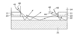
- FIG. it is a figure which shows the optical path of incident light when the surface position of a colored layer is flat at the back surface side of a solar cell.
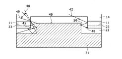
- it is a figure which shows the optical path of incident light when the surface position of a colored layer is made into the position of the pn junction of a solar cell.
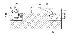
- it is a figure which shows the optical path of incident light when the surface position of a colored layer is set between the position of the pn junction of a solar cell, and the position of the light-receiving surface of a solar cell.
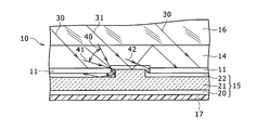
- FIG. 1 is a cross-sectional view showing the structure of the solar cell module 10.
- the solar cell 11 which comprises the solar cell module 10 has as a main surface the light-receiving surface which is a surface into which the light from the exterior of the solar cell 11 mainly injects, and the back surface which is a surface on the opposite side to a light-receiving surface.
- the upper side of the paper surface is the light receiving surface side
- the lower side is the back surface side.
- the solar cell module 10 is obtained by sandwiching a plurality of solar cells 11 connected in series using a plurality of wiring members 12 and 13 between a sealing material 14 on the light receiving surface side and a sealing material 15 on the back surface side.
- the protective member 16 on the light receiving surface side and the protective member 17 on the back surface side are arranged on the front, and the ends are fixed by frames 18 and 19.
- the solar cell 11 includes a photoelectric conversion unit that generates light-generated carriers of holes and electrons by receiving light such as sunlight.
- the photoelectric conversion unit includes a substrate made of a semiconductor material such as crystalline silicon (c-Si), gallium arsenide (GaAs), indium phosphide (InP), for example.
- the structure of the photoelectric conversion unit is a pn junction in a broad sense. For example, a heterojunction of an n-type single crystal silicon substrate and amorphous silicon can be used.
- a transparent conductive film (TCO) composed of a conductive oxide is laminated, and an i-type amorphous silicon layer and an n-type amorphous silicon layer doped with phosphorus (P) or the like on the back side of the substrate, A transparent conductive film can be laminated.
- the photoelectric conversion unit may have a structure other than this as long as it has a function of converting light such as sunlight into electricity.
- a structure including a p-type polycrystalline silicon substrate, an n-type diffusion layer formed on the light-receiving surface side, and an aluminum metal film formed on the back surface side may be used.
- the wiring members 12 and 13 are conductive members that are connected to a connection electrode formed on the surface of the transparent conductive film on the photoelectric conversion portion using a conductive paste or the like via an adhesive.
- a connection electrode formed on the surface of the transparent conductive film on the photoelectric conversion portion using a conductive paste or the like via an adhesive.
- thin plates made of a metal conductive material such as copper are used. Instead of a thin plate, a stranded wire can be used.
- the conductive material in addition to copper, silver, aluminum, nickel, tin, gold, or an alloy thereof can be used.
- thermosetting resin adhesive such as acrylic, highly flexible polyurethane, or epoxy
- the adhesive includes conductive particles.
- conductive particles nickel, silver, nickel with gold coating, copper with tin plating, or the like can be used.
- An insulating resin adhesive can also be used as the adhesive. In this case, either one or both of the wiring members 12 and 13 or the facing surfaces of the connection electrodes are made uneven to appropriately remove the resin from between the wiring members 12 and 13 and the connection electrodes. Try to establish a dynamic connection.
- the sealing material 14 on the light receiving surface side and the sealing material 15 on the back surface side are sheet-like members having a role as a shock buffering material and a function of preventing intrusion of foreign matter and moisture with respect to the solar cell 11. .
- These sealing materials 14 and 15 are selected in consideration of heat resistance, adhesiveness, flexibility, moldability, durability, and the like.
- the encapsulant 14 on the light receiving surface side is made of a transparent encapsulant that has as high transparency as possible so as to take in light from the outside, and transmits incident light without absorbing or reflecting.
- polyethylene-based olefin resin, ethylene vinyl acetate (EVA), or the like is used.
- EVA ethylene vinyl acetate
- EEA, PVB, silicone resin, urethane resin, acrylic resin, epoxy resin, and the like can be used.
- the back surface side sealing material 15 may be the same material as the light receiving surface side sealing material 14, but here, light from the light receiving surface side of the solar cell 11 is directed to the back surface side of the solar cell 11.
- a sealing material having a laminated structure including a colored layer colored in white is used. That is, the sealing material 15 on the back surface side is configured by a three-layer laminated structure of the transparent layer 20, the colored layer 21, and the transparent layer 22 from the back surface side protection member 17 side toward the solar cell 11 side.
- the transparent layers 20 and 22 may be made of the same material as the sealing material 14 on the light receiving surface side. When distinguishing the transparent layers 20 and 22, the former can be called the transparent layer 20 on the back surface protection member side, and the latter can be called the transparent layer 22 on the solar cell side.
- the colored layer 21 can be obtained by mixing a colorant into a transparent sealing material.
- EVA EVA or the like can be used.
- an inorganic pigment such as titanium oxide or zinc oxide can be used as a coloring material for coloring in white.
- the refractive index of a transparent underlayer such as EVA is about 1.49 to 1.50, and the refractive index of titanium oxide is about 2.5.
- the colored layer 21 is mixed with about 1 to 5% of titanium oxide by mass ratio. Preferably 3% is mixed.
- the colored layer 21 has a higher light reflectivity than the transparent layers 20 and 21 and functions as a reflective layer.
- a colored layer 21 other than white may be used by using an appropriate inorganic pigment other than white.
- the colored layer 21 is the thickest, and the thin transparent layers 20 and 22 are arranged on both sides thereof.
- the colored layer 21 is about 300 to 400 ⁇ m, and the transparent layers 20 and 22 are about 100 ⁇ m.
- the protective member 16 on the light receiving surface side is a transparent plate or film that can take in light from the outside.
- a translucent member such as a glass plate, a resin plate, or a resin film can be used.
- the same protective member 17 on the back surface side as the protective member 16 on the light receiving surface side can be used.
- an opaque plate or film can be used as the protective member 17 on the back side.
- a laminated film such as a resin film having an aluminum foil inside can be used.
- FIG. 2 is an enlarged view showing a gap portion sandwiched between adjacent solar cells 11 in order to explain the function of the sealing material 15 on the back surface side as a reflective layer.
- a wiring member 13 for connecting the adjacent solar cells 11 is arranged in a part of the gap between the adjacent solar cells 11.
- the wiring member is shown to show the light path.
- positioned was abbreviate
- the gap between adjacent solar cells 11 is the center, and the two solar cells 11 are arranged symmetrically with respect to this gap.
- the colored layer 21 protrudes to the light receiving surface side from the back surface of the solar cell 11, but does not protrude to the position of the light receiving surface of the solar cell 11. Details of setting the surface position of the colored layer 21 will be described later.
- FIG. 2 shows the optical paths of some of the light incident on the solar cell module 10. As an optical path, some examples are shown for some light beams from the upper left to the lower right of the page. Since the end portions of the two solar cells 11 are arranged symmetrically on the paper surface, the light traveling from the upper right to the lower left of the paper surface with respect to the right solar cell 11 in FIG. 2 is symmetric with the light traveling from the upper left to the lower right. It may be considered that it acts on.
- the light 30 incident on the light receiving surface of the solar cell 11 is absorbed by the light receiving surface of the solar cell 11 without being affected by the sealing material 15 on the back surface side and contributes to power generation.
- a part of the light 31 incident on the gap between the adjacent solar cells 11 is transmitted through the transparent layer 22 and reflected by the surface of the colored layer 21, and the light-receiving surface side sealing material 14 and the light-receiving surface-side protection member 16 The light is reflected at the interface between the two, travels toward the back side again, and enters the light receiving surface of the solar cell 11.
- the incident light from the light receiving surface side is incident on the light receiving surface of the solar cell 11, although there is a difference between direct incident and indirect incident, except for light incident on the transparent layer 22.
- the transparent layer 22 sandwiched between the solar cell 11 and the colored layer 21 serves as a light guide for guiding incident light from the light receiving surface side of the solar cell 11 to the side surface and the back surface of the solar cell 11.
- the light incident on the transparent layer 22 and reflected on the side surface of the colored layer 21 and then incident on the back surface of the solar cell 11 and the light incident on the side surface of the solar cell 11 contribute to power generation on the back surface side of the solar cell 11.
- the light 40, 41, 42 incident on the transparent layer 22 the light 40, 41 is incident on the transparent layer 22 and is first reflected by the side surface of the colored layer 21, and then the side surface of the solar cell 11 and It has an optical path toward the back side.
- the light 42 enters the transparent layer 22 and is first reflected by the side surface of the solar cell 11, and then reflected by the side surface of the colored layer 21, and has an optical path toward the side surface and the back surface of the solar cell 11.
- these lights 40, 41, and 42 contribute to power generation on the light receiving surface side of the solar cell 11 like the lights 30 and 31, but are colored with the solar cell 11.
- the function of the light guide layer of the transparent layer 22 sandwiched between the layers 21 contributes to power generation on the back side of the solar cell 11.
- the surface position of the colored layer 21 is largely related to the degree of contribution of power generation on the back side of the solar cell 11 of the light incident on the transparent layer 22.
- the relationship between the surface position of the colored layer 21 and the power generation on the back side will be described in detail with reference to FIGS. These figures are further enlarged views of FIG.
- the position of the pn junction 23 in the solar cell 11 is shown as a reference.
- the light 43 and 44 is incident on the transparent layer 22, then reflected on the surface of the colored layer 21, not on the side surface, and incident on the back surface of the solar cell 11.
- the light 43 and 44 contribute to the power generation on the back side of the solar cell 11, and these are not the light reflected by the side surfaces of the colored layer 21.
- FIG. 4 is a diagram showing a state in which the transparent layer 22 and the colored layer 21 are arranged on the back surface side of the solar cell 11 so as to have side surfaces raised along the corners 45 on the back surface side of the solar cell 11. is there.
- the transparent layer 22 and the colored layer 21 cover the corner 45.
- the surface position 46 of the colored layer 21 is a position closer to the light receiving surface than the position of the back surface of the solar cell 11.
- the surface position 46 of the colored layer 21 is shown as the same position as the position of the pn junction 23. This is an example beyond the position of the back surface of the solar cell 11 and may not be the same as the position of the pn junction 23.
- the transparent layer 22 and the colored layer 21 protrude from the position of the back surface of the solar cell 11 toward the light receiving surface side in the gap between the adjacent solar cells 11.
- light 40 and 41 is the same as that described in FIG. 2, and is incident on the transparent layer 22, first reflected on the side surface of the colored layer 21, and then incident on the back surface side of the solar cell 11.
- the light 40 enters the transparent layer 22 from the end of the light receiving surface of the solar cell 11 and has an optical path that reaches the rising corner of the colored layer 21.
- the light 41 is light that enters the transparent layer 22 from the end of the light receiving surface of the solar cell 11 and travels toward the top corner of the colored layer 21 at the rising edge.
- the light 41 is reflected by the surface of the colored layer 21 on the back surface side of the solar cell 11 after being reflected by the corner portion at the top of the colored layer 21, and has an optical path toward the back surface of the solar cell 11.
- the “colored layer primary reflected light” contributing to power generation on the back side is light having an incident angle in a range between the incident angle of the light 40 and the incident angle of the light 41.
- the incident angle of the light 40 is an incident angle from the end of the light receiving surface of the solar cell 11 toward the rising corner of the colored layer 21, and the incident angle of the light 41 is the colored layer from the end of the light receiving surface of the solar cell 11. It is an incident angle toward the corner of the top of 21 rise.
- the light 42 is the same as that described with reference to FIG. 2, and the light incident on the transparent layer 22 and reflected by the side surface of the solar cell 11 hits the corner 47 at the top of the colored layer 21, and from there the solar cell 11. It has an optical path that hits the corner 48 on the back surface.
- FIG. 5 is a diagram illustrating a case where the surface position 46 of the colored layer 21 is closer to the light receiving surface side of the solar cell 11 than in the case of FIG. 4 but does not exceed the position of the light receiving surface of the solar cell 11.
- the surface position 46 of the colored layer 21 is the position of the pn junction 23
- the surface position 46 of the colored layer 21 in FIG. 5 is the position of the pn junction 23
- the light 49 is light that enters the transparent layer 22 from the end of the light receiving surface of the solar cell 11 and travels toward the top corner of the colored layer 21 as light 41 in FIG. 4. Since the position of the corner of the top of the colored layer 21 is the surface position 46 of the colored layer 21, the incident angle of the light 49 from the end of the light receiving surface of the solar cell 11 toward the corner of the top of the colored layer 21 is Compared to the light 41 in FIG. 4, the light receiving surface of the solar cell 11 has an angle closer to parallel.
- the “colored layer primary reflected light” contributing to power generation on the back side is light having an incident angle in a range between the incident angle of the light 40 and the incident angle of the light 41 in FIG. And an incident angle in a range between the incident angle of the light 49 and the incident angle of the light 49. Therefore, compared with FIG. 4, the light used as "colored layer primary reflected light” increases in FIG.
- the light 42 is incident on the side surface of the solar cell 11 at the same position as the light 42 in FIG. 4, but the position 50 where the light reflected by the side surface of the solar cell 11 hits the side surface of the colored layer 21 is It is on the back side with respect to the corner 47 at the top of the rise.
- the “colored layer secondary reflected light” that contributes to power generation on the back side is light on the back side with respect to the corner portion 47 at the top of the colored layer 21, but the light 42 is the limit in FIG. 4.
- FIG. 5 light whose incident angle is perpendicular to the light 42 is reflected by the side surface of the solar cell 11 and hits the corner portion 47 at the top of the colored layer 21. Accordingly, the amount of light that becomes “colored layer secondary reflected light” increases.
- FIG. 6 is a diagram illustrating a case where the surface position 46 of the colored layer 21 is the position of the light receiving surface of the solar cell 11.
- the light 51 having an optical path that is incident on the transparent layer 22 from the end of the light receiving surface of the solar cell 11 and is reflected at the corner of the top of the colored layer 21 becomes light along the surface of the light receiving surface of the solar cell 11.
- the “colored layer primary reflected light” that contributes to power generation on the back side in FIG. 6 is light having an incident angle in a range between the incident angle of the light 40 and the incident angle of the light 51.
- light that becomes “colored layer primary reflected light” further increases, but this is the limit of increase.
- FIG. 7 is a diagram illustrating a case where the surface position 46 of the colored layer 21 exceeds the position of the light receiving surface of the solar cell 11 and becomes the protective member 16 side on the light receiving surface side. Since the increase in “colored layer primary reflected light” has already reached its limit in FIG. 6, the illustration is omitted. In “colored layer secondary reflected light”, light incident on the side surface of the solar cell 11 is limited as compared with FIG. 6. The light 42 is the same as the light 42 in FIG. 5, but the surface position 46 of the colored layer 21 exceeds the position of the light receiving surface of the solar cell 11, so that the light 42 is reflected on the surface of the colored layer 21. 11 is not incident on the side surface.
- the light 53 is light that is incident on the end of the light receiving surface of the solar cell 11 from the corner of the top of the colored layer 21, and this is the limit of “colored layer secondary reflected light”. Although the optical path of the light 53 is shown as it is in FIG. 6, the light 53 in FIG. 6 has a sufficient margin to the limit of “colored layer secondary reflected light”.
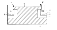
- FIG. 8 is a diagram showing a case where the surface position 46 of the colored layer 21 is further on the side of the protective member 16 on the light receiving surface side and has overhang portions 54 and 55 that partially cover the end portions of the light receiving surface of the solar cell 11. It is.
- the colored layer 21 has such overhang portions 54 and 55, the light 56 and 57 incident on these portions are reflected by the colored layer 21, and the effective power generation area on the light receiving surface side of the solar cell 11 is increased. Decrease.
- the “colored layer secondary reflected light” may be restricted as shown in FIG.
- the effective power generation area on the light receiving surface side does not decrease.
- the transparent layer The light incident on 22 can be efficiently contributed to power generation on the back surface side of the solar cell 11.
- the surface position of the colored layer 21 is set by adding the sealing material 14 on the light receiving surface side and the sealing material 15 on the back surface side, and sandwiching between the protection member 16 on the light receiving surface side and the protection member 17 on the back surface side. This can be done by adjusting the pressure.
Landscapes
- Photovoltaic Devices (AREA)
- Life Sciences & Earth Sciences (AREA)
- Sustainable Development (AREA)
- Health & Medical Sciences (AREA)
- Molecular Biology (AREA)
Description
本発明は、裏面封止材を有する太陽電池モジュールに関する。
太陽電池モジュールは、太陽電池に対する耐環境性を向上させるため、太陽電池の受光面側と裏面側にそれぞれ封止材を配置し、その外側に保護部材を配置する構造を取る。
例えば、特許文献1には、太陽電池の発電効率を上げるため、太陽電池素子の背面側の封止材として、白色顔料を含ませた白色封止材を用い、これにて太陽光を反射させ、太陽電池素子の背面側に反射光を入射させることが述べられている。
特許文献2には、隣り合う太陽電池セルの間の領域に対応して光を反射する反射部材を裏面部材側に選択的に設けた先行技術を述べている。そしてこの先行技術の構造は、太陽電池セルの端部と反射部材の端部との間の位置合わせの精度が必要で、僅かに位置ずれした場合でも光反射部材を有効に利用できない問題があると述べ、また、表面部材に斜めから浅い角度で入ってくる光は反射部材に当たらず、そのまま裏面部材を通過することを指摘している。そこで、太陽電池セルと反射層の間の距離を最適化する計算式を提案している。
裏面封止材に着色層を用いるときに、着色層の反射を利用して、太陽電池の側面に入射する光を裏面側発電に寄与させることである。
本発明に係る太陽電池モジュールは、太陽電池と、太陽電池の裏面側に配置された裏面封止材と、を備え、裏面封止材は、太陽電池の受光面側からの光を反射する着色層と、着色層と太陽電池との間に設けられる透明層と、を含み、透明層は、隣接する太陽電池の間の隙間において、太陽電池の裏面側の角部に沿って立ち上げられた側面を有する。
太陽電池の側面に入射する光を太陽電池の裏面側に誘導でき、裏面発電に寄与できる。
以下に図面を用いて、本発明の実施の形態を詳細に説明する。以下で述べる材質、厚さ、寸法等は説明のための例示であって、太陽電池モジュールの仕様に応じ、適宜変更が可能である。以下では、全ての図面において一または対応する要素には同一の符号を付し、重複する説明を省略する。
図1は、太陽電池モジュール10の構造を示す断面図である。太陽電池モジュール10を構成する太陽電池11は、主面として、太陽電池11の外部からの光が主に入射する面である受光面と、受光面と反対側の面である裏面とを有するが、図1では、紙面の上側を受光面側、下側を裏面側とした。
太陽電池モジュール10は、複数の太陽電池11を複数の配線材12,13を用いて互いに直列接続したものを、受光面側の封止材14と裏面側の封止材15で挟み、その外側に受光面側の保護部材16と裏面側の保護部材17を配置し、端部をフレーム18,19で固定して構成される。
太陽電池11は、太陽光等の光を受光することで正孔および電子の光生成キャリアを生成する光電変換部を備える。光電変換部は、例えば、結晶性シリコン(c-Si)、ガリウム砒素(GaAs)、インジウム燐(InP)等の半導体材料の基板を有する。光電変換部の構造は、広義のpn接合である。例えば、n型単結晶シリコン基板と非晶質シリコンのヘテロ接合を用いることができる。この場合、受光面側の基板上に、i型非晶質シリコン層と、ボロン(B)等がドープされたp型非晶質シリコン層と、酸化インジウム(In2O3)の透光性導電酸化物で構成される透明導電膜(TCO)を積層し、基板の裏面側に、i型非晶質シリコン層と、燐(P)等がドープされたn型非晶質シリコン層と、透明導電膜を積層する構造とできる。
光電変換部は、太陽光等の光を電気に変換する機能を有すれば、これ以外の構造であってもよい。例えば、p型多結晶シリコン基板と、その受光面側に形成されたn型拡散層と、その裏面側に形成されたアルミニウム金属膜とを備える構造であってもよい。
配線材12,13は、光電変換部の上の透明導電膜の表面に導電ペースト等を用いて形成された接続用電極に接着剤を介して接続される導電性部材である。配線材12,13としては、銅等の金属導電性材料で構成される薄板が用いられる。薄板に代えて撚り線状のものを用いることもできる。導電性材料としては、銅の他に、銀、アルミニウム、ニッケル、錫、金、あるいはこれらの合金を用いることができる。
接着剤としては、アクリル系、柔軟性の高いポリウレタン系、あるいはエポキシ系等の熱硬化性樹脂接着剤を用いることができる。接着剤には、導電性粒子が含まれる。導電性粒子としては、ニッケル、銀、金コート付ニッケル、錫メッキ付銅等を用いることができる。接着剤として、絶縁性の樹脂接着剤を用いることもできる。この場合には、配線材12,13または接続用電極の互いに対向する面のいずれか一方または双方を凹凸化して、配線材12,13と接続用電極の間から樹脂を適当に排除して電気的接続を取るようにする。
受光面側の封止材14と裏面側の封止材15は、太陽電池11に対し、衝撃の緩衝材としての役割と、異物や水分の侵入を防ぐ機能等を有するシート状の部材である。これらの封止材14,15は、耐熱性、接着性、柔軟性、成形性、耐久性等を考慮して材質が選定される。受光面側の封止材14は、外部からの光を取り入れるため、できるだけ高い透明性を有し、入射した光を吸収したり反射することなく透過させる透明封止材が用いられる。例えば、ポリエチレン系のオレフィン樹脂やエチレンビニルアセテート(EVA)等が用いられる。その他に、EEA、PVB、シリコーン系樹脂、ウレタン系樹脂、アクリル系樹脂、エポキシ系樹脂等を用いることもできる。
裏面側の封止材15は、受光面側の封止材14と同じ材質のものを用いることができるが、ここでは、太陽電池11の受光面側からの光を太陽電池11の裏面側に導入させるように、白色に着色された着色層を含む積層構造の封止材が用いられる。すなわち、裏面側の封止材15は、裏面側の保護部材17の側から太陽電池11の側に向かって、透明層20、着色層21、透明層22の三層の積層構造で構成される。透明層20,22は、受光面側の封止材14と同じ材質のものを用いることができる。透明層20,22を区別するときは、前者を裏面保護部材側の透明層20、後者を太陽電池側の透明層22と呼ぶことができる。
着色層21は、透明な封止材に着色材を混入させて得ることができる。下地の透明な封止材としては、EVA等を用いることができ、例えば、白色に着色するには、酸化チタンや酸化亜鉛等の無機顔料を着色材として用いることができる。EVA等の透明な下地層の屈折率は約1.49~1.50で、酸化チタンの屈折率は約2.5である。着色層21は、質量比で酸化チタンを約1~5%混入させる。好ましくは3%混入することがよい。これによって、着色層21は、透明層20,21に比べて光の反射率が高くなり、反射層としての働きをする。白色以外の適当な無機顔料等を用いて、白色以外の着色層21としてもよい。
裏面側の封止材15の厚さは、着色層21が最も厚く、その両側に薄い厚さの透明層20,22が配置される。厚さの一例を上げると、着色層21が約300-400μm、透明層20,22がそれぞれ約100μmである。
受光面側の保護部材16は、外部から光を取り入れることができる透明な板体、フィルムである。受光面側の保護部材16としては、ガラス板、樹脂板、樹脂フィルム等の透光性を有する部材を用いることができる。裏面側の保護部材17は、受光面側の保護部材16と同じものを用いることができる。裏面側からの受光を必要としない構造の太陽電池モジュール10の場合は、裏面側の保護部材17として、不透明な板体やフィルムを用いることができる。例えば、アルミ箔を内部に有する樹脂フィルム等の積層フィルムを用いることができる。
図2は、裏面側の封止材15の反射層としての機能を説明するために、隣接する太陽電池11に挟まれた隙間の部分を拡大して示す図である。隣接する太陽電池11で挟まれた隙間の一部の領域には、隣接する太陽電池11の間を接続する配線材13が配置されるが、図2では光の経路を示すために、配線材13が配置されていない領域を省略した。
図2では、隣接する太陽電池11に挟まれた隙間を中央とし、2つの太陽電池11をこの隙間に対し対称配置とした。隣接する太陽電池11で挟まれた隙間において、着色層21は太陽電池11の裏面よりも受光面側に突き出すが、太陽電池11の受光面の位置までは突き出さない。着色層21の表面位置の設定の詳細については後述する。
図2において、太陽電池モジュール10に入射する光のいくつかについてその光路を示した。光路としては、紙面の左上から右下に向かういくつかの光についていくつかの例を示してある。2つの太陽電池11の端部は、紙面で左右対称に配置されているので、図2で右側の太陽電池11に対し紙面の右上から左下に向かう光は、左上から右下に向かう光と対称に作用するものと考えればよい。
図2において、太陽電池11の受光面に入射する光30は、裏面側の封止材15に影響されることなく太陽電池11の受光面に吸収されて発電に寄与する光である。隣接する太陽電池11の隙間に入射する光31の一部は、透明層22を透過して着色層21の表面で反射され、受光面側の封止材14と受光面側の保護部材16との間の界面で反射されて再び裏面側に向かい、太陽電池11の受光面に入射する。このように、受光面側からの入射光は、透明層22に入射する光を除いて、直接入射か間接入射かの差はあるが、太陽電池11の受光面に入射する。
一方、透明層20,22と比べて着色層21は反射率が高いので、隣接する太陽電池11の隙間に入射する光31のうち太陽電池11と着色層21に挟まれた透明層22に入射した光は、透明層22と着色層21の界面で反射され、太陽電池11の側面及び裏面に向かうことになる。なお、透明層22に比べて太陽電池11の側面も反射率が高いので、透明層22と太陽電池11との界面では、太陽電池11に吸収されなかった光が着色層21に向けて反射されることになる。すなわち、太陽電池11と着色層21に挟まれた透明層22に入射した光は、着色層21と太陽電池11の間で反射されて、太陽電池11の側面および裏面に向かう。このように、太陽電池11と着色層21に挟まれた透明層22は、太陽電池11の受光面側からの入射光を太陽電池11の側面および裏面に導く導光路の役割をする。
透明層22に入射し着色層21の側面で反射し、その後太陽電池11の裏面に入射した光や、太陽電池11の側面に入射した光は、太陽電池11の裏面側における発電に寄与する。図2において、透明層22に入射する光40,41,42のうち、光40,41は、透明層22に入射してまず着色層21の側面で反射され、その後、太陽電池11の側面および裏面に向かう光路を有する。光42は、透明層22に入射してまず太陽電池11の側面で反射され、その後着色層21の側面で反射されて、太陽電池11の側面および裏面に向かう光路を有する。
これらの光40,41,42は、透明層22と着色層21がなければ、光30,31のように太陽電池11の受光面側の発電に寄与するものであるが、太陽電池11と着色層21に挟まれた透明層22の導光層の機能によって、太陽電池11の裏面側の発電に寄与するようになる。
着色層21の表面位置は、透明層22に入射した光の太陽電池11の裏面側の発電の寄与の程度に大きく関係する。図3から図8を用いて、着色層21の表面位置と裏面側の発電との関係について詳細に説明する。これらの図は、図2をさらに拡大した図である。ここでは、参考として太陽電池11におけるpn接合23の位置が示されている。
図3は、透明層22と着色層21が平坦で、隣接する太陽電池11で挟まれた隙間において透明層22が太陽電池11の裏面の位置からは突き出していない場合を示す図である。光40,41,42は、図2の光40,41,42と同じ入射角度の光である。図2と異なり、隣接する太陽電池11に挟まれた領域に着色層21の側面が形成されていないので、着色層21の側面で反射されることなく着色層21の表面で反射されるだけである。これらの光は、再び受光側の封止材14と受光面側の保護部材16の界面で反射され、太陽電池11の受光面に入射する。なお、光43,44は、透明層22に入射した後、着色層21の側面でなく表面で反射し、太陽電池11の裏面に入射するものである。図3において太陽電池11の裏面側の発電に寄与するのは、光43,44で、これらは着色層21の側面で反射した光ではない。
図4は、太陽電池11の裏面側において、太陽電池11の裏面側の角部45に沿って立ち上げられた側面を有するように、透明層22と着色層21を配置したときを示す図である。ここでは透明層22と着色層21が角部45の周りを覆っている。ここで、着色層21の表面位置46は、太陽電池11の裏面の位置よりも受光面側の位置である。1つの目安として、着色層21の表面位置46がpn接合23の位置と同じ位置として示されている。これは太陽電池11の裏面の位置を越えている一例であって、pn接合23の位置と同じでなくても構わない。ここでは、隣接する太陽電池11で挟まれた隙間において透明層22と着色層21が太陽電池11の裏面の位置から受光面側に向けて突き出る。
図4において、光40,41は、図2で説明したものと同じで、透明層22に入射した後、最初に着色層21の側面に反射し、その後太陽電池11の裏面側に入射する光路を有する。光40は、太陽電池11の受光面の端部から透明層22に入射し、着色層21の立上りの隅部に達する光路を有する。光41は、太陽電池11の受光面の端部から透明層22に入射し着色層21の立上りの頂部の角部に向かう光である。光41は、着色層21の立上りの頂部の角部で反射された後、太陽電池11の裏面側における着色層21の表面で反射し、太陽電池11の裏面に向かう光路を有する。
透明層22に入射した後、最初に着色層21の側面に反射し、その後太陽電池11の裏面側に入射するタイプの光路を有する光を、「着色層1次反射光」と呼ぶことにすると、図4の場合、裏面側の発電に寄与する「着色層1次反射光」は、光40の入射角度と光41の入射角度の間の範囲の入射角度を有する光である。光40の入射角度は、太陽電池11の受光面の端部から着色層21の立上りの隅部に向かう入射角度で、光41の入射角度は、太陽電池11の受光面の端部から着色層21の立上りの頂部の角部に向かう入射角度である。
光42も図2で説明したものと同じで、透明層22に入射し、太陽電池11の側面で反射した光がちょうど着色層21の立上りの頂部の角部47に当たり、そこから太陽電池11の裏面の角部48に当たる光路を有する。
透明層22に入射し、最初に太陽電池11の側面で反射し、その後着色層21の側面で反射されて、太陽電池11の側面に入射するタイプの光路を有する光を、「着色層2次反射光」と呼ぶことにすると、着色層21の立上りの頂部の角部47の位置、すなわち着色層21の表面位置が太陽電池11の裏面の位置よりも受光面側にあるときに初めて「着色層2次反射光」が発生することになる。図4の光42はその限界の「着色層2次反射光」に相当する。
図5は、着色層21の表面位置46が、図4の場合よりも太陽電池11の受光面側であるが、太陽電池11の受光面の位置を越えないときを示す図である。図4では着色層21の表面位置46をpn接合23の位置としたので、図5の着色層21の表面位置46はpn接合23よりも受光面側として示した。
光49は、図4の光41のように、太陽電池11の受光面の端部から透明層22に入射し、着色層21の頂部の角部に向かう光である。着色層21の頂部の角部の位置は、着色層21の表面位置46であるので、太陽電池11の受光面の端部から着色層21の頂部の角部に向かう光49の入射角度は、図4の光41に比べ、太陽電池11の受光面により平行に近い角度となる。裏面側の発電に寄与する「着色層1次反射光」は、図4では光40の入射角度と光41の入射角度の間の範囲の入射角度を有する光であるが、図5では光40の入射角度と光49の入射角度の間の範囲の入射角度を有する光である。したがって、図4に比べ、「着色層1次反射光」となる光が図5では増加する。
光42は、太陽電池11の側面に入射する位置が図4の光42と同じであるが、太陽電池11の側面で反射した光が着色層21の側面に当る位置50が、着色層21の立上りの頂部の角部47よりも裏面側となる。裏面側の発電に寄与する「着色層2次反射光」は、着色層21の立上りの頂部の角部47よりも裏面側の光であるが、図4では光42がその限界であった。図5では、入射角度が光42よりも垂直側の光が太陽電池11の側面で反射して着色層21の立上りの頂部の角部47に当ることになる。その分、「着色層2次反射光」となる光が増加することになる。
図6は、着色層21の表面位置46が、太陽電池11の受光面の位置となるときを示す図である。太陽電池11の受光面の端部から透明層22に入射し、着色層21の頂部の角部で反射する光路を有する光51は、太陽電池11の受光面の表面に沿った光となる。したがって、図6において裏面側の発電に寄与する「着色層1次反射光」は、光40の入射角度と光51の入射角度の間の範囲の入射角度を有する光でとなるので、図5に比べ、「着色層1次反射光」となる光がさらに増加するが、これが増加の限界となる。
光42は、図4、図5の光42と同じであるが、太陽電池11の側面で反射した光が着色層21の側面に当る位置52が、着色層21の立上りの頂部の角部47よりもさらに裏面側となる。その分、「着色層2次反射光」となる光がさらに増加することになる。なお、光53は、太陽電池11の受光面の端部に入射し、そこで反射して着色層21の側壁に当たり、さらに反射して太陽電池11の裏面に向かう光路を有する光の一例を示すもので、次の図7で裏面発電寄与の限界となる光53を先取りして示したものである。
図7は、着色層21の表面位置46が、太陽電池11の受光面の位置を越えて受光面側の保護部材16の側となるときを示す図である。「着色層1次反射光」の増加は図6で既に限界となっているので、図示を省略した。「着色層2次反射光」は、太陽電池11の側面に入射する光が図6に比べ制限される。光42は、図5の光42と同じものであるが、着色層21の表面位置46が太陽電池11の受光面の位置を越えることから、着色層21の表面で反射されてしまい、太陽電池11の側面に入射されない。光53が着色層21の立上りの頂部の角部から太陽電池11の受光面の端部に入射する光で、これが「着色層2次反射光」の限界となる。図6でこの光53の光路をそのまま示したが、図6における光53は「着色層2次反射光」の限界まで十分余裕がある。
図8は、着色層21の表面位置46が、さらに受光面側の保護部材16の側となり、太陽電池11の受光面の端部を一部覆う張出部54,55を有するときを示す図である。着色層21がこのような張出部54,55を有すると、この部分に入射した光56,57は着色層21で反射されてしまい、太陽電池11の受光面側の実効的な発電面積が減少する。
なお、この張出部54,55が発生するまでは、図7に示すように、「着色層2次反射光」は制限を受けることがあるが、透明層22の存在によって、太陽電池11の受光面側の実効的な発電面積が減少することはない。
このように、着色層21の表面位置が、太陽電池11の裏面側の位置よりも受光面側で、太陽電池11の受光面の位置よりも裏面側になるように設定することで、透明層22に入射した光を太陽電池11の裏面側における発電に効率的に寄与させることができる。着色層21の表面位置の設定は、受光面側の封止材14と裏面側の封止材15を配置して、受光面側の保護部材16と裏面側の保護部材17で挟み込むときの加圧力の調整等で行うことができる。
10 太陽電池モジュール、11 太陽電池、12,13 配線材、14 (受光面側の)封止材、15 (裏面側の)封止材、16 (受光面側の)保護部材、17 (裏面側の)保護部材、18,19 フレーム、20,22 透明層、21 着色層、23 pn接合、30,31,40,41,42,43,44,49,51,53,56,57 光、45,47,48 角部、46 (着色層の)表面位置、50,52 位置、54,55 張出部。
Claims (3)
- 太陽電池と、
前記太陽電池の裏面側に配置された裏面封止材と、
を備え、
前記裏面封止材は、
前記太陽電池の受光面側からの光を反射する着色層と、
前記着色層と前記太陽電池との間に設けられる透明層と、
を含み、
前記透明層は、隣接する前記太陽電池の間の隙間において、前記太陽電池の前記裏面側の角部に沿って立ち上げられた側面を有する、太陽電池モジュール。 - 請求項1に記載の太陽電池モジュールにおいて、
前記着色層は、隣接する前記太陽電池の間の隙間において、前記太陽電池の裏面側の位置よりも前記太陽電池の前記受光面側に表面を有する、太陽電池モジュール。 - 請求項2に記載の太陽電池モジュールにおいて、
前記着色層は、隣接する前記太陽電池の間の隙間において、前記太陽電池の前記受光面の位置よりも前記裏面側に表面を有する、太陽電池モジュール。
Priority Applications (4)
| Application Number | Priority Date | Filing Date | Title |
|---|---|---|---|
| EP12882267.3A EP2881996A4 (en) | 2012-07-31 | 2012-07-31 | SOLAR CELL MODULE |
| PCT/JP2012/069496 WO2014020708A1 (ja) | 2012-07-31 | 2012-07-31 | 太陽電池モジュール |
| JP2014527878A JP5999571B2 (ja) | 2012-07-31 | 2012-07-31 | 太陽電池モジュール |
| US14/602,754 US9502588B2 (en) | 2012-07-31 | 2015-01-22 | Solar cell module |
Applications Claiming Priority (1)
| Application Number | Priority Date | Filing Date | Title |
|---|---|---|---|
| PCT/JP2012/069496 WO2014020708A1 (ja) | 2012-07-31 | 2012-07-31 | 太陽電池モジュール |
Related Child Applications (1)
| Application Number | Title | Priority Date | Filing Date |
|---|---|---|---|
| US14/602,754 Continuation US9502588B2 (en) | 2012-07-31 | 2015-01-22 | Solar cell module |
Publications (1)
| Publication Number | Publication Date |
|---|---|
| WO2014020708A1 true WO2014020708A1 (ja) | 2014-02-06 |
Family
ID=50027438
Family Applications (1)
| Application Number | Title | Priority Date | Filing Date |
|---|---|---|---|
| PCT/JP2012/069496 Ceased WO2014020708A1 (ja) | 2012-07-31 | 2012-07-31 | 太陽電池モジュール |
Country Status (4)
| Country | Link |
|---|---|
| US (1) | US9502588B2 (ja) |
| EP (1) | EP2881996A4 (ja) |
| JP (1) | JP5999571B2 (ja) |
| WO (1) | WO2014020708A1 (ja) |
Cited By (4)
| Publication number | Priority date | Publication date | Assignee | Title |
|---|---|---|---|---|
| JP2016187022A (ja) * | 2015-03-27 | 2016-10-27 | パナソニックIpマネジメント株式会社 | 太陽電池モジュール |
| WO2018088323A1 (ja) * | 2016-11-10 | 2018-05-17 | 三井化学東セロ株式会社 | 太陽電池裏面側封止シートセット、太陽電池モジュールおよび太陽電池モジュールの製造方法 |
| WO2018088322A1 (ja) * | 2016-11-10 | 2018-05-17 | 三井化学東セロ株式会社 | 太陽電池裏面側封止シートセット、太陽電池モジュールおよび太陽電池モジュールの製造方法 |
| JP2018082073A (ja) * | 2016-11-17 | 2018-05-24 | 信越化学工業株式会社 | 太陽電池モジュールの製造方法 |
Families Citing this family (4)
| Publication number | Priority date | Publication date | Assignee | Title |
|---|---|---|---|---|
| WO2017037231A1 (en) * | 2015-09-02 | 2017-03-09 | Sabic Global Technologies B.V. | Solar panel and method of manufacturing such a solar panel |
| US20180309003A1 (en) * | 2017-04-24 | 2018-10-25 | Helion Concepts, Inc. | Lightweight solar panels with solar cell structural protection |
| KR102398146B1 (ko) * | 2020-02-14 | 2022-05-13 | 고려대학교 산학협력단 | 컬러 태양 전지 모듈 |
| DE102023108236A1 (de) * | 2023-03-30 | 2024-10-02 | Hanwha Q Cells Gmbh | Solarmodul und verwendung einer eva-schicht |
Citations (6)
| Publication number | Priority date | Publication date | Assignee | Title |
|---|---|---|---|---|
| JPH06177412A (ja) * | 1992-12-10 | 1994-06-24 | Bridgestone Corp | 太陽電池封止材膜 |
| JP2006036874A (ja) | 2004-07-26 | 2006-02-09 | Du Pont Mitsui Polychem Co Ltd | 太陽電池封止用エチレン共重合体組成物及びそれを用いた太陽電池モジュール |
| JP2006073707A (ja) * | 2004-09-01 | 2006-03-16 | Kyocera Corp | 太陽電池モジュール |
| JP2006286789A (ja) | 2005-03-31 | 2006-10-19 | Sanyo Electric Co Ltd | 太陽電池モジュール |
| JP2007335853A (ja) * | 2006-05-18 | 2007-12-27 | Dainippon Printing Co Ltd | 太陽電池モジュール用充填材およびこれを用いた太陽電池モジュール |
| JP2011216804A (ja) * | 2010-04-02 | 2011-10-27 | Bridgestone Corp | 太陽電池用封止膜、これを用いた太陽電池、及び太陽電池の製造方法 |
Family Cites Families (3)
| Publication number | Priority date | Publication date | Assignee | Title |
|---|---|---|---|---|
| US4321417A (en) * | 1978-06-30 | 1982-03-23 | Exxon Research & Engineering Co. | Solar cell modules |
| JP2007033583A (ja) | 2005-07-25 | 2007-02-08 | Tomoegawa Paper Co Ltd | 電子写真用トナー |
| JP2010287688A (ja) * | 2009-06-10 | 2010-12-24 | Mitsubishi Electric Corp | 太陽電池モジュール |
-
2012
- 2012-07-31 WO PCT/JP2012/069496 patent/WO2014020708A1/ja not_active Ceased
- 2012-07-31 EP EP12882267.3A patent/EP2881996A4/en not_active Withdrawn
- 2012-07-31 JP JP2014527878A patent/JP5999571B2/ja active Active
-
2015
- 2015-01-22 US US14/602,754 patent/US9502588B2/en not_active Expired - Fee Related
Patent Citations (6)
| Publication number | Priority date | Publication date | Assignee | Title |
|---|---|---|---|---|
| JPH06177412A (ja) * | 1992-12-10 | 1994-06-24 | Bridgestone Corp | 太陽電池封止材膜 |
| JP2006036874A (ja) | 2004-07-26 | 2006-02-09 | Du Pont Mitsui Polychem Co Ltd | 太陽電池封止用エチレン共重合体組成物及びそれを用いた太陽電池モジュール |
| JP2006073707A (ja) * | 2004-09-01 | 2006-03-16 | Kyocera Corp | 太陽電池モジュール |
| JP2006286789A (ja) | 2005-03-31 | 2006-10-19 | Sanyo Electric Co Ltd | 太陽電池モジュール |
| JP2007335853A (ja) * | 2006-05-18 | 2007-12-27 | Dainippon Printing Co Ltd | 太陽電池モジュール用充填材およびこれを用いた太陽電池モジュール |
| JP2011216804A (ja) * | 2010-04-02 | 2011-10-27 | Bridgestone Corp | 太陽電池用封止膜、これを用いた太陽電池、及び太陽電池の製造方法 |
Non-Patent Citations (1)
| Title |
|---|
| See also references of EP2881996A4 |
Cited By (6)
| Publication number | Priority date | Publication date | Assignee | Title |
|---|---|---|---|---|
| JP2016187022A (ja) * | 2015-03-27 | 2016-10-27 | パナソニックIpマネジメント株式会社 | 太陽電池モジュール |
| WO2018088323A1 (ja) * | 2016-11-10 | 2018-05-17 | 三井化学東セロ株式会社 | 太陽電池裏面側封止シートセット、太陽電池モジュールおよび太陽電池モジュールの製造方法 |
| WO2018088322A1 (ja) * | 2016-11-10 | 2018-05-17 | 三井化学東セロ株式会社 | 太陽電池裏面側封止シートセット、太陽電池モジュールおよび太陽電池モジュールの製造方法 |
| JPWO2018088323A1 (ja) * | 2016-11-10 | 2019-03-28 | 三井化学東セロ株式会社 | 太陽電池裏面側封止シートセット、太陽電池モジュールおよび太陽電池モジュールの製造方法 |
| JPWO2018088322A1 (ja) * | 2016-11-10 | 2019-03-28 | 三井化学東セロ株式会社 | 太陽電池裏面側封止シートセット、太陽電池モジュールおよび太陽電池モジュールの製造方法 |
| JP2018082073A (ja) * | 2016-11-17 | 2018-05-24 | 信越化学工業株式会社 | 太陽電池モジュールの製造方法 |
Also Published As
| Publication number | Publication date |
|---|---|
| JP5999571B2 (ja) | 2016-09-28 |
| US20150129015A1 (en) | 2015-05-14 |
| JPWO2014020708A1 (ja) | 2016-07-11 |
| EP2881996A1 (en) | 2015-06-10 |
| EP2881996A4 (en) | 2015-09-02 |
| US9502588B2 (en) | 2016-11-22 |
Similar Documents
| Publication | Publication Date | Title |
|---|---|---|
| JP5999571B2 (ja) | 太陽電池モジュール | |
| US10879410B2 (en) | Solar cell module | |
| US20170148942A1 (en) | Solar panel and method of manufacturing such a solar panel | |
| US20130340804A1 (en) | Solar cell module and ribbon assembly applied to the same | |
| EP3067937B1 (en) | Solar cell module | |
| JPWO2014050004A1 (ja) | 太陽電池モジュール | |
| CN108475706B (zh) | 太阳能电池模块 | |
| JP2018163988A (ja) | 太陽電池モジュール | |
| TWI545790B (zh) | 光電變換裝置 | |
| CN108701734B (zh) | 太阳能电池组件 | |
| CN106356410A (zh) | 高功率太阳能电池模块 | |
| US20150214410A1 (en) | Solar cell module | |
| US10784392B2 (en) | Solar cell module and method for manufacturing the same | |
| KR101616131B1 (ko) | 태양전지 모듈 | |
| CN104205619B (zh) | 太阳能电池装置 | |
| JP4924724B2 (ja) | 太陽電池パネル | |
| US10629763B2 (en) | Solar cell module | |
| JP4656982B2 (ja) | 太陽電池モジュール | |
| JP6224696B2 (ja) | 太陽電池モジュール | |
| JP2012151240A (ja) | 太陽電池モジュール | |
| TWM523192U (zh) | 高功率太陽能電池模組 | |
| WO2014033924A1 (ja) | 太陽電池モジュール | |
| TWM523193U (zh) | 高功率太陽能電池模組 | |
| TW201729428A (zh) | 高功率太陽能電池模組 | |
| KR20160074098A (ko) | 태양전지 모듈용 리본, 이를 포함하는 태양전지 모듈 및 이의 제조방법 |
Legal Events
| Date | Code | Title | Description |
|---|---|---|---|
| 121 | Ep: the epo has been informed by wipo that ep was designated in this application |
Ref document number: 12882267 Country of ref document: EP Kind code of ref document: A1 |
|
| ENP | Entry into the national phase |
Ref document number: 2014527878 Country of ref document: JP Kind code of ref document: A |
|
| WWE | Wipo information: entry into national phase |
Ref document number: 2012882267 Country of ref document: EP |
|
| NENP | Non-entry into the national phase |
Ref country code: DE |