WO2014024310A1 - 半導体素子、hemt素子、および半導体素子の製造方法 - Google Patents
半導体素子、hemt素子、および半導体素子の製造方法 Download PDFInfo
- Publication number
- WO2014024310A1 WO2014024310A1 PCT/JP2012/070521 JP2012070521W WO2014024310A1 WO 2014024310 A1 WO2014024310 A1 WO 2014024310A1 JP 2012070521 W JP2012070521 W JP 2012070521W WO 2014024310 A1 WO2014024310 A1 WO 2014024310A1
- Authority
- WO
- WIPO (PCT)
- Prior art keywords
- layer
- semiconductor device
- iii nitride
- group iii
- manufacturing
- Prior art date
- Legal status (The legal status is an assumption and is not a legal conclusion. Google has not performed a legal analysis and makes no representation as to the accuracy of the status listed.)
- Ceased
Links
Images
Classifications
-
- H—ELECTRICITY
- H10—SEMICONDUCTOR DEVICES; ELECTRIC SOLID-STATE DEVICES NOT OTHERWISE PROVIDED FOR
- H10D—INORGANIC ELECTRIC SEMICONDUCTOR DEVICES
- H10D30/00—Field-effect transistors [FET]
- H10D30/40—FETs having zero-dimensional [0D], one-dimensional [1D] or two-dimensional [2D] charge carrier gas channels
- H10D30/47—FETs having zero-dimensional [0D], one-dimensional [1D] or two-dimensional [2D] charge carrier gas channels having two-dimensional [2D] charge carrier gas channels, e.g. nanoribbon FETs or high electron mobility transistors [HEMT]
-
- H—ELECTRICITY
- H10—SEMICONDUCTOR DEVICES; ELECTRIC SOLID-STATE DEVICES NOT OTHERWISE PROVIDED FOR
- H10D—INORGANIC ELECTRIC SEMICONDUCTOR DEVICES
- H10D30/00—Field-effect transistors [FET]
- H10D30/01—Manufacture or treatment
- H10D30/015—Manufacture or treatment of FETs having heterojunction interface channels or heterojunction gate electrodes, e.g. HEMT
-
- H—ELECTRICITY
- H10—SEMICONDUCTOR DEVICES; ELECTRIC SOLID-STATE DEVICES NOT OTHERWISE PROVIDED FOR
- H10D—INORGANIC ELECTRIC SEMICONDUCTOR DEVICES
- H10D30/00—Field-effect transistors [FET]
- H10D30/40—FETs having zero-dimensional [0D], one-dimensional [1D] or two-dimensional [2D] charge carrier gas channels
- H10D30/47—FETs having zero-dimensional [0D], one-dimensional [1D] or two-dimensional [2D] charge carrier gas channels having two-dimensional [2D] charge carrier gas channels, e.g. nanoribbon FETs or high electron mobility transistors [HEMT]
- H10D30/471—High electron mobility transistors [HEMT] or high hole mobility transistors [HHMT]
- H10D30/475—High electron mobility transistors [HEMT] or high hole mobility transistors [HHMT] having wider bandgap layer formed on top of lower bandgap active layer, e.g. undoped barrier HEMTs such as i-AlGaN/GaN HEMTs
-
- H—ELECTRICITY
- H10—SEMICONDUCTOR DEVICES; ELECTRIC SOLID-STATE DEVICES NOT OTHERWISE PROVIDED FOR
- H10D—INORGANIC ELECTRIC SEMICONDUCTOR DEVICES
- H10D62/00—Semiconductor bodies, or regions thereof, of devices having potential barriers
- H10D62/80—Semiconductor bodies, or regions thereof, of devices having potential barriers characterised by the materials
- H10D62/82—Heterojunctions
- H10D62/824—Heterojunctions comprising only Group III-V materials heterojunctions, e.g. GaN/AlGaN heterojunctions
-
- H—ELECTRICITY
- H10—SEMICONDUCTOR DEVICES; ELECTRIC SOLID-STATE DEVICES NOT OTHERWISE PROVIDED FOR
- H10D—INORGANIC ELECTRIC SEMICONDUCTOR DEVICES
- H10D64/00—Electrodes of devices having potential barriers
- H10D64/60—Electrodes characterised by their materials
- H10D64/602—Heterojunction gate electrodes for FETs
-
- H—ELECTRICITY
- H10—SEMICONDUCTOR DEVICES; ELECTRIC SOLID-STATE DEVICES NOT OTHERWISE PROVIDED FOR
- H10D—INORGANIC ELECTRIC SEMICONDUCTOR DEVICES
- H10D64/00—Electrodes of devices having potential barriers
- H10D64/60—Electrodes characterised by their materials
- H10D64/66—Electrodes having a conductor capacitively coupled to a semiconductor by an insulator, e.g. MIS electrodes
- H10D64/68—Electrodes having a conductor capacitively coupled to a semiconductor by an insulator, e.g. MIS electrodes characterised by the insulator, e.g. by the gate insulator
- H10D64/693—Electrodes having a conductor capacitively coupled to a semiconductor by an insulator, e.g. MIS electrodes characterised by the insulator, e.g. by the gate insulator the insulator comprising nitrogen, e.g. nitrides, oxynitrides or nitrogen-doped materials
-
- H—ELECTRICITY
- H10—SEMICONDUCTOR DEVICES; ELECTRIC SOLID-STATE DEVICES NOT OTHERWISE PROVIDED FOR
- H10P—GENERIC PROCESSES OR APPARATUS FOR THE MANUFACTURE OR TREATMENT OF DEVICES COVERED BY CLASS H10
- H10P14/00—Formation of materials, e.g. in the shape of layers or pillars
- H10P14/20—Formation of materials, e.g. in the shape of layers or pillars of semiconductor materials
- H10P14/24—Formation of materials, e.g. in the shape of layers or pillars of semiconductor materials using chemical vapour deposition [CVD]
-
- H—ELECTRICITY
- H10—SEMICONDUCTOR DEVICES; ELECTRIC SOLID-STATE DEVICES NOT OTHERWISE PROVIDED FOR
- H10P—GENERIC PROCESSES OR APPARATUS FOR THE MANUFACTURE OR TREATMENT OF DEVICES COVERED BY CLASS H10
- H10P14/00—Formation of materials, e.g. in the shape of layers or pillars
- H10P14/20—Formation of materials, e.g. in the shape of layers or pillars of semiconductor materials
- H10P14/29—Formation of materials, e.g. in the shape of layers or pillars of semiconductor materials characterised by the substrates
- H10P14/2901—Materials
-
- H—ELECTRICITY
- H10—SEMICONDUCTOR DEVICES; ELECTRIC SOLID-STATE DEVICES NOT OTHERWISE PROVIDED FOR
- H10P—GENERIC PROCESSES OR APPARATUS FOR THE MANUFACTURE OR TREATMENT OF DEVICES COVERED BY CLASS H10
- H10P14/00—Formation of materials, e.g. in the shape of layers or pillars
- H10P14/20—Formation of materials, e.g. in the shape of layers or pillars of semiconductor materials
- H10P14/29—Formation of materials, e.g. in the shape of layers or pillars of semiconductor materials characterised by the substrates
- H10P14/2901—Materials
- H10P14/2902—Materials being Group IVA materials
- H10P14/2904—Silicon carbide
-
- H—ELECTRICITY
- H10—SEMICONDUCTOR DEVICES; ELECTRIC SOLID-STATE DEVICES NOT OTHERWISE PROVIDED FOR
- H10P—GENERIC PROCESSES OR APPARATUS FOR THE MANUFACTURE OR TREATMENT OF DEVICES COVERED BY CLASS H10
- H10P14/00—Formation of materials, e.g. in the shape of layers or pillars
- H10P14/20—Formation of materials, e.g. in the shape of layers or pillars of semiconductor materials
- H10P14/29—Formation of materials, e.g. in the shape of layers or pillars of semiconductor materials characterised by the substrates
- H10P14/2901—Materials
- H10P14/2902—Materials being Group IVA materials
- H10P14/2905—Silicon, silicon germanium or germanium
-
- H—ELECTRICITY
- H10—SEMICONDUCTOR DEVICES; ELECTRIC SOLID-STATE DEVICES NOT OTHERWISE PROVIDED FOR
- H10P—GENERIC PROCESSES OR APPARATUS FOR THE MANUFACTURE OR TREATMENT OF DEVICES COVERED BY CLASS H10
- H10P14/00—Formation of materials, e.g. in the shape of layers or pillars
- H10P14/20—Formation of materials, e.g. in the shape of layers or pillars of semiconductor materials
- H10P14/32—Formation of materials, e.g. in the shape of layers or pillars of semiconductor materials characterised by intermediate layers between substrates and deposited layers
- H10P14/3202—Materials thereof
- H10P14/3214—Materials thereof being Group IIIA-VA semiconductors
- H10P14/3216—Nitrides
-
- H—ELECTRICITY
- H10—SEMICONDUCTOR DEVICES; ELECTRIC SOLID-STATE DEVICES NOT OTHERWISE PROVIDED FOR
- H10P—GENERIC PROCESSES OR APPARATUS FOR THE MANUFACTURE OR TREATMENT OF DEVICES COVERED BY CLASS H10
- H10P14/00—Formation of materials, e.g. in the shape of layers or pillars
- H10P14/20—Formation of materials, e.g. in the shape of layers or pillars of semiconductor materials
- H10P14/32—Formation of materials, e.g. in the shape of layers or pillars of semiconductor materials characterised by intermediate layers between substrates and deposited layers
- H10P14/3242—Structure
- H10P14/3244—Layer structure
- H10P14/3248—Layer structure consisting of two layers
-
- H—ELECTRICITY
- H10—SEMICONDUCTOR DEVICES; ELECTRIC SOLID-STATE DEVICES NOT OTHERWISE PROVIDED FOR
- H10P—GENERIC PROCESSES OR APPARATUS FOR THE MANUFACTURE OR TREATMENT OF DEVICES COVERED BY CLASS H10
- H10P14/00—Formation of materials, e.g. in the shape of layers or pillars
- H10P14/20—Formation of materials, e.g. in the shape of layers or pillars of semiconductor materials
- H10P14/34—Deposited materials, e.g. layers
- H10P14/3402—Deposited materials, e.g. layers characterised by the chemical composition
- H10P14/3414—Deposited materials, e.g. layers characterised by the chemical composition being group IIIA-VIA materials
- H10P14/3416—Nitrides
-
- H—ELECTRICITY
- H10—SEMICONDUCTOR DEVICES; ELECTRIC SOLID-STATE DEVICES NOT OTHERWISE PROVIDED FOR
- H10P—GENERIC PROCESSES OR APPARATUS FOR THE MANUFACTURE OR TREATMENT OF DEVICES COVERED BY CLASS H10
- H10P14/00—Formation of materials, e.g. in the shape of layers or pillars
- H10P14/60—Formation of materials, e.g. in the shape of layers or pillars of insulating materials
- H10P14/63—Formation of materials, e.g. in the shape of layers or pillars of insulating materials characterised by the formation processes
- H10P14/6326—Deposition processes
- H10P14/6349—Deposition of epitaxial materials
-
- H—ELECTRICITY
- H10—SEMICONDUCTOR DEVICES; ELECTRIC SOLID-STATE DEVICES NOT OTHERWISE PROVIDED FOR
- H10D—INORGANIC ELECTRIC SEMICONDUCTOR DEVICES
- H10D62/00—Semiconductor bodies, or regions thereof, of devices having potential barriers
- H10D62/80—Semiconductor bodies, or regions thereof, of devices having potential barriers characterised by the materials
- H10D62/85—Semiconductor bodies, or regions thereof, of devices having potential barriers characterised by the materials being Group III-V materials, e.g. GaAs
- H10D62/8503—Nitride Group III-V materials, e.g. AlN or GaN
Definitions
- the present invention relates to a semiconductor element, and more particularly to a semiconductor element having a Schottky diode junction between a multilayer structure epitaxial substrate made of a group III nitride semiconductor and a metal electrode.
- Nitride semiconductors are attracting attention as semiconductor materials for next-generation high-frequency / high-power devices because they have a high breakdown electric field and a high saturation electron velocity.
- a HEMT (High Electron Mobility Transistor) element formed by laminating a barrier layer made of AlGaN and a channel layer made of GaN has a laminated interface due to a large polarization effect (spontaneous polarization effect and piezoelectric polarization effect) peculiar to nitride materials.
- This utilizes the feature that a high-concentration two-dimensional electron gas (2DEG) is generated at the (heterointerface) (see, for example, Non-Patent Document 1).
- 2DEG high-concentration two-dimensional electron gas
- a single crystal (heterogeneous single crystal) having a composition different from that of a group III nitride such as silicon or SiC may be used.
- a buffer layer such as a strained superlattice layer or a low temperature growth buffer layer is generally formed on the base substrate as an initial growth layer. Therefore, epitaxially forming the barrier layer, the channel layer, and the buffer layer on the base substrate is the most basic configuration of the HEMT element substrate using the base substrate made of different single crystals.
- a spacer layer having a thickness of about 1 nm may be provided between the barrier layer and the channel layer for the purpose of promoting spatial confinement of the two-dimensional electron gas.
- the spacer layer is made of, for example, AlN. Furthermore, a cap layer made of, for example, an n-type GaN layer or a superlattice layer is formed on the barrier layer for the purpose of controlling the energy level at the outermost surface of the substrate for HEMT elements and improving the contact characteristics with the electrode. Sometimes it is done.
- the concentration of the two-dimensional electron gas existing in the substrate for the HEMT device is It is known that it increases with an increase in the AlN mole fraction of AlGaN to be formed (see, for example, Non-Patent Document 2). If the two-dimensional electron gas concentration can be significantly increased, it is considered that the controllable current density of the HEMT element, that is, the power density that can be handled, can be significantly improved.
- the strain is less dependent on the piezoelectric polarization effect and can generate a two-dimensional electron gas at a high concentration only by spontaneous polarization.
- a HEMT element having a small number of structures is also attracting attention (see, for example, Non-Patent Document 3).
- the junction between the gate electrode and the barrier layer is generally a Schottky junction.
- a large leakage current may be generated when a reverse voltage is applied to the Schottky junction.
- This leakage current can be reduced by forming a contact layer made of AlN on the InAlN layer.
- the HEMT element having such a configuration has a low mobility of the two-dimensional electron gas. Occurs. This is presumed to be caused by distortion in the InAlN layer because the lattice constant of the AlN layer is smaller than that of the InAlN layer.
- the present invention has been made in view of the above problems, and an object thereof is to provide a semiconductor element in which reverse leakage current is suppressed and the mobility of a two-dimensional electron gas is high.
- an epitaxial substrate in which a group (III) nitride layer group is formed on a base substrate so that the (0001) crystal plane is substantially parallel to the substrate surface;
- the film thickness of the intermediate layer is 0.5 nm or more.
- the film thickness of the intermediate layer is 6 nm or less.
- the thickness of the cap layer is 0.5 nm or more and 6 nm or less.
- the band gap of the second group III nitride is larger than the band gap of the first group III nitride. I made it bigger.
- the Schottky electrode includes at least one of Ni, Pt, Pd, and Au.
- the root mean square surface roughness of the cap layer is 0.5 nm or less.
- the first group III nitride is GaN.
- the third group III nitride is AlN.
- an ohmic electrode is bonded to the same cap layer as the Schottky electrode.
- the Schottky electrode is a gate electrode
- the ohmic electrode is a source electrode and a drain electrode.
- an epitaxial substrate obtained by stacking a group III nitride layer group on a base substrate so that a (0001) crystal plane is substantially parallel to the substrate surface, and a Schottky electrode
- the intermediate layer is formed to a thickness of 0.5 nm or more.
- the intermediate layer is formed to a thickness of 6 nm or less.
- the cap layer is formed to a thickness of 0.5 nm or more and 6 nm or less.
- the band gap of the second group III nitride is the band of the first group III nitride. It was made larger than the gap.
- the Schottky electrode in the method for manufacturing a semiconductor device according to any one of the fifteenth to nineteenth aspects, is formed of Ni, Pt, Pd, It was formed so as to include at least one of Au.
- the first group III nitride is GaN.
- the third group III nitride is AlN.
- the method for manufacturing a semiconductor device includes an ohmic property in which an ohmic electrode is bonded to the cap layer on which the Schottky electrode is formed.
- An electrode forming step includes an ohmic property in which an ohmic electrode is bonded to the cap layer on which the Schottky electrode is formed.
- the intermediate layer made of GaN and the cap layer made of AlN are provided in this order on the barrier layer, and electrodes are formed on the cap layer by Schottky junction,
- the MIS junction By forming the MIS junction, the reverse leakage current is suppressed and the mobility of the two-dimensional electron gas is kept high as compared with the case where the electrode is formed directly on the barrier layer by the Schottky junction.
- a semiconductor element is realized.
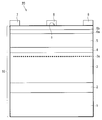
- FIG. 1 It is a cross-sectional schematic diagram which shows roughly the structure of the HEMT element 20 which is one aspect
- FIG. 1 is a schematic cross-sectional view schematically showing a configuration of a HEMT element 20 which is an aspect of a semiconductor element according to an embodiment of the present invention.
- the HEMT element 20 generally has a configuration in which a source electrode 7, a drain electrode 8, and a gate electrode 9 are provided on an epitaxial substrate 10.
- the epitaxial substrate 10 has a configuration in which a base substrate 1, a buffer layer 2, a channel layer 3, a spacer layer 4, a barrier layer 5, an intermediate layer 6a, and a cap layer 6b are stacked.
- Have A source electrode 7, a drain electrode 8, and a gate electrode 9 are formed on the cap layer 6b.
- the buffer layer 2, the channel layer 3, the spacer layer 4, the barrier layer 5, the intermediate layer 6a, and the cap layer 6b are all formed epitaxially using MOCVD (metal organic chemical vapor deposition). (A detail will be described later) is a suitable example.
- MOCVD metal organic chemical vapor deposition
- each layer will be described.
- other epitaxial growth methods such as MBE, HVPE, and LPE can be used as long as each layer can be formed so as to have good crystallinity.
- a method appropriately selected from various vapor phase growth methods and liquid phase growth methods may be used, or a mode in which different growth methods are used in combination may be used.
- the base substrate 1 can be used without any particular limitation as long as a nitride semiconductor layer with good crystallinity can be formed thereon.
- a single crystal 6H—SiC substrate is preferably used, but an embodiment using a substrate made of sapphire, Si, GaAs, spinel, MgO, ZnO, ferrite, or the like may be used.
- the buffer layer 2 is made of several hundreds of nanometers in AlN in order to improve the crystal quality of the channel layer 3, the spacer layer 4, the barrier layer 5, the intermediate layer 6a, and the cap layer 6b formed thereon. It is a layer formed to a certain thickness. For example, it is a preferable example that the thickness is 200 nm.
- the channel layer 3 and the barrier layer 5 have a composition range in which the band gap of the second group III nitride constituting the latter is larger than the band gap of the first group III nitride constituting the former. It is formed.
- the intermediate layer 6a is a layer formed of GaN.
- the cap layer 6b is a layer formed of AlN. The effect of the HEMT element 20 having these intermediate layer 6a and cap layer 6b will be described later.
- a two-dimensional electron gas is present at a high concentration at the interface between the channel layer 3 and the spacer layer 4 (more specifically, near the interface of the channel layer 3).
- An electron gas region 3e is formed.
- the spacer layer 4 is a binary compound of Al and N, the alloy scattering effect is further suppressed as compared with the case of a ternary compound containing Ga, and the concentration and mobility of the two-dimensional electron gas are improved. It will be. Note that the discussion on the composition range does not exclude that the spacer layer 4 contains impurities.
- spacer layer 4 in the epitaxial substrate 10 is not an essential aspect, and may be an aspect in which the barrier layer 5 is formed directly on the channel layer 3. In such a case, a two-dimensional electron gas region 3 e is formed at the interface between the channel layer 3 and the barrier layer 5.
- the source electrode 7 and the drain electrode 8 are multi-layer metal electrodes in which each metal layer has a thickness of about 10 to 100 nm, and has an ohmic contact with the cap layer 6b.
- the metal used for the source electrode 7 and the drain electrode 8 should just be formed with the metal material with which favorable ohmic contact is obtained with respect to the epitaxial substrate 10 (with respect to the cap layer 6b).
- An embodiment in which a multilayer metal electrode made of Al or the like may be formed.
- the source electrode 7 and the drain electrode 8 can be formed by a photolithography process and a vacuum deposition method.
- the gate electrode 9 is a single-layer or multi-layer metal electrode in which one or a plurality of metal layers are formed so as to have a thickness of about ten to several hundreds of nanometers. It has a Schottky contact.
- the gate electrode 9 is preferably formed using a metal having a high work function such as Pd, Pt, Ni, or Au as a forming material. Or the aspect formed as a multilayer metal film of the above-mentioned each metal or each metal, Al, etc. may be sufficient.
- the cap layer 6b made of AlN is provided, in addition to the above, a metal material used for forming an ohmic junction with a group III nitride semiconductor such as a multilayer metal film containing Ti / Al is also used for the gate. It can be used as a material for forming the electrode 9. This is because, in this case, AlN having a large band gap and a metal material having a relatively small work function are joined, so that a Schottky contact can be obtained relatively easily.
- the gate electrode 9 can be formed by a photolithography process and a vacuum deposition method.
- a so-called MIS (metal-insulator-semiconductor) junction is formed by the gate electrode 9, the cap layer 6b, and the barrier layer 5 (strictly, through the intermediate layer 6a). Is formed.
- the HEMT element 20 has, in principle, a reverse leakage current suppressed more than a conventional HEMT element in which the gate electrode 9 is directly Schottky-bonded to the barrier layer 5. Become.
- a leakage current when -100 V is applied is directly applied to the barrier electrode in the barrier layer. Is suppressed from about 1/100 to about 1/1000 when formed.
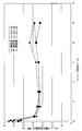
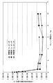
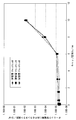
- FIG. 2 to 4 are diagrams for explaining the effect of providing the cap layer 6b immediately below the gate electrode 9 in the HEMT element, that is, the effect of the HEMT element having the MIS junction described above.
- FIG. 2 shows that the composition of the barrier layer 5 is changed to three levels of In 0.14 Al 0.86 N, In 0.18 Al 0.82 N, and In 0.24 Al 0.76 N.
- the relationship between the surface roughness of the cap layer 6b and its thickness is illustrated.
- the intermediate layer 6a is not provided for the HEMT element for the sake of easy discussion.
- FIG. 3 illustrates the relationship between the reverse leakage current and the thickness of the cap layer 6b for the same HEMT element.
- FIG. 4 illustrates the relationship between the contact resistance and the thickness of the cap layer 6b for the same HEMT element.
- the value is maximum when the thickness of the cap layer 6b is 0 nm (that is, when the cap layer 6b is not provided), and the value is between the thickness of the cap layer 6b up to 0.5 nm. Drops sharply, and at 0.5 nm or more, it is almost flat at a smaller value (0.5 nm or less) than at 0 nm. This is because the surface flatness is improved by forming the cap layer 6b to a thickness of 0.5 nm or more, and the gate electrode 9 is provided on the cap layer 6b having excellent surface flatness. This means that the reverse leakage current is reduced. Further, the surface of the cap layer 6 b is flattened more than the surface of the barrier layer 5.
- the contact resistance is substantially constant at 1.0 ⁇ 10 ⁇ 5 / ⁇ cm 2 or less, whereas the thickness of the cap layer 6b is 6 nm. It can be seen that the contact resistance increases abruptly when the value is exceeded. This result indicates that the thickness of the cap layer 6b should be 6 nm or less from the viewpoint of keeping the contact resistance of the ohmic electrode at a sufficiently low value.
- the cap layer 6b is preferably formed to a thickness of 0.5 nm or more and 6 nm or less.
- the HEMT device 20 includes an intermediate layer 6a between the barrier layer 5 and the cap layer 6b. This is to keep the mobility of the two-dimensional electron gas high. More specifically, when the cap layer 6b as described above is formed directly on the barrier layer 5, the mobility of the two-dimensional electron gas is reduced. Therefore, in the present embodiment, this is suppressed.
- an intermediate layer 6a is formed on the barrier layer 5, and a cap layer 6b is formed thereon.
- the thickness of the intermediate layer 6a is preferably 0.5 nm or more and 6 nm or less. By forming it to a thickness of 0.5 nm or more, higher mobility is realized as compared with the case where the intermediate layer 6a is not provided.
- the upper limit of the thickness of the intermediate layer 6a may be determined within a range that is kept low without affecting the sheet resistance. For example, if the thickness of the cap layer 6b is 0.5 nm or more and 6 nm or less, the sheet resistance is reduced to 300 ⁇ / ⁇ or less by setting the thickness of the intermediate layer 6a to (0.5 nm or more) 6 nm or less.
- the intermediate layer 6a and the cap layer 6b are entirely formed on the barrier layer 5, and not only directly below the gate electrode 9, but also directly below the source electrode 7 and the drain electrode 8. It can be said that it is also characteristic in that it is uniformly provided. Originally, if the intermediate layer 6a and the cap layer 6b exist only directly under the gate electrode 9, the effect of reducing the reverse leakage current can be obtained, but in order to realize such a configuration, photolithography is required. A process, an etching process, and the like are required, which causes a high cost.
- the intermediate layer 6a and the cap layer 6b are only formed on the barrier layer 5 entirely, and since such a process is not performed, a HEMT device having excellent characteristics while suppressing cost is realized. It can be said that it is done.
- the cap layer 6b, the intermediate layer 6a, and a part of the barrier layer 5 are removed by etching before forming both electrodes. After performing ohmic, the aspect which forms the source electrode 7 and the drain electrode 8 on the barrier layer 5 exposed by this may be sufficient.
- the epitaxial substrate 10 can be manufactured using a known MOCVD furnace. Specifically, organometallic (MO) source gases (TMI, TMA, TMG), ammonia gas (NH 3 gas), hydrogen gas, and nitrogen gas for In, Al, and Ga can be supplied into the reactor.
- MOCVD furnace constructed as follows is used.
- a 2 inch 6H-SiC substrate having a (0001) plane orientation is prepared as a base substrate 1, and the base substrate 1 is placed on a susceptor provided in a reactor of an MOCVD furnace. After replacing the inside of the reactor with vacuum gas, the temperature of the substrate is raised by susceptor heating after forming an atmosphere in a hydrogen / nitrogen mixed flow state while maintaining the reactor pressure at a predetermined value between 5 kPa and 50 kPa.
- the susceptor temperature reaches a predetermined temperature (for example, 1050 ° C.) between 950 ° C. and 1250 ° C. which is the buffer layer formation temperature, Al source gas and NH 3 gas are introduced into the reactor, and the AlN layer as the buffer layer 2 is formed.
- a predetermined temperature for example, 1050 ° C.
- 950 ° C. and 1250 ° C. which is the buffer layer formation temperature
- Al source gas and NH 3 gas are introduced into the reactor, and the AlN layer as the buffer layer 2 is formed.
- the susceptor temperature is maintained at a predetermined channel layer formation temperature, an organometallic source gas and ammonia gas corresponding to the composition of the channel layer 3 are introduced into the reactor, and In x1 Al as the channel layer 3 is introduced.
- the channel layer formation temperature T1 is a value determined according to the value of the AlN molar fraction y1 of the channel layer 3 from a temperature range of 950 ° C. or more and 1250 ° C. or less.
- the reactor pressure at the time of forming the channel layer 3 is not particularly limited, and can be appropriately selected from the range of 10 kPa to atmospheric pressure (100 kPa).
- the reactor When the In x1 Al y1 Ga z1 N layer is formed, the reactor is maintained in a nitrogen gas atmosphere with the susceptor temperature maintained, the reactor pressure is set to 10 kPa, and the organometallic source gas and ammonia gas are then reacted with the reactor. Then, an In x3 Al y3 Ga z3 N layer as the spacer layer 4 is formed to a predetermined thickness.
- the susceptor temperature is maintained at a predetermined barrier layer forming temperature of 650 ° C. or higher and 800 ° C. or lower in order to form In x2 Al y2 N to be the barrier layer 5.
- the internal pressure is maintained at a predetermined value between 1 kPa and 30 kPa.
- ammonia gas and an organic metal source gas having a flow rate ratio corresponding to the composition of the barrier layer 5 are introduced into the reactor so that the so-called V / III ratio is a predetermined value between 3000 and 20000.
- the susceptor temperature is set to a predetermined intermediate layer formation temperature, TMG and NH 3 gas are supplied, and the GaN layer as the intermediate layer 6a is formed. A predetermined thickness is formed.
- TMA and NH 3 gas are supplied after the susceptor temperature is set to a predetermined cap layer forming temperature, and an AlN layer as the cap layer 6b is formed to a predetermined thickness. . If the cap layer 6b is formed, the epitaxial substrate 10 is manufactured.
- a HEMT element is formed using this.
- Each subsequent process is realized by a known method.
- a multilayer metal pattern to be the source electrode 7 and the drain electrode 8 is formed at a formation target portion of the cap layer 6b by using a photolithography process and a vacuum deposition method.
- a nitrogen gas atmosphere at a predetermined temperature of 650 ° C. to 1000 ° C. is applied to the epitaxial substrate 10 on which the source electrode 7 and the drain electrode 8 are formed. Inside, heat treatment is performed for several tens of seconds.
- a multilayer metal pattern to be the gate electrode 9 is formed at a formation target portion of the cap layer 6b by using a photolithography process and a vacuum deposition method.
- HEMT elements 20 are obtained by dicing into chips of a predetermined size.
- the obtained HEMT element 20 is appropriately subjected to die bonding or wire bonding.
- the intermediate layer made of GaN is provided on the barrier layer, the cap layer made of AlN is further provided, and the gate electrode is formed by Schottky junction to the cap layer.
- the MIS junction By forming the MIS junction, the reverse leakage current is greatly reduced as compared with the case where the gate electrode is formed directly on the barrier layer by the Schottky junction, and the two-dimensional electron gas is formed.
- a HEMT element having a high mobility is realized.
- the HEMT element is described as an object.
- an aspect in which the MIS junction is formed between the gate electrode and the barrier layer is another electronic device using a Schottky junction, for example, a shot
- a Schottky junction for example, a shot
- the cap layer 6b is formed of AlN, but the cap layer 6b is larger than the band gap of the second group III nitride and has an insulating group III nitride. It may be an aspect formed by.
- the group III nitride has insulation means that the specific resistance is 10 8 ⁇ cm or more. If it has the specific resistance of the range, the MIS junction mentioned above is formed suitably. In addition, as long as the specific resistance is satisfied, the presence of conductive impurities is allowed in the cap layer 6b.
- Example 1 Comparative Example 1, and Comparative Example
- the epitaxial substrate 10 according to the above-described embodiment including the intermediate layer 6a and the cap layer 6b is prepared, and the two-dimensional electron gas concentration, the mobility of the two-dimensional electron gas, and the sheet resistance And evaluated.
- the epitaxial substrate 10 using this epitaxial substrate 10, four types of HEMT elements 20 having different configurations of the gate electrode 9 were produced, and the reverse leakage current when ⁇ 100 V was applied to each HEMT element 20 was evaluated.
- Comparative Example 1 an epitaxial substrate not including both the intermediate layer 6a and the cap layer 6b was prepared, and the two-dimensional electron gas concentration, the mobility of the two-dimensional electron gas, and the sheet resistance were evaluated.
- four types of HEMT devices were fabricated by forming the gate electrode 9 on the epitaxial substrate in the same manner as in Example 1, and the reverse leakage current when -100 V was applied was evaluated for each HEMT device. .
- Comparative Example 2 an epitaxial substrate provided with only the cap layer 6b without the intermediate layer 6a was prepared, and the two-dimensional electron gas concentration, the mobility of the two-dimensional electron gas, and the sheet resistance were evaluated.
- four types of HEMT devices were fabricated by forming the gate electrode 9 on the epitaxial substrate in the same manner as in Example 1, and the reverse leakage current when -100 V was applied was evaluated for each HEMT device. .
- a total of 12 types of HEMT elements were obtained by forming four types of gate electrodes 9 having different configurations on three types of epitaxial substrates.
- an epitaxial substrate 10 was produced. At that time, all the epitaxial substrates 10 were subjected to the same conditions until the formation of the spacer layer 4.
- the base substrate 1 a plurality of 2 inch 6H—SiC substrates having a (0001) plane orientation were prepared. The thickness was 300 ⁇ m. About each board
- the susceptor temperature was set to a predetermined temperature
- TMG bubbling gas as an organic metal source gas and ammonia gas were introduced into the reactor at a predetermined flow ratio, and a GaN layer as a channel layer 3 was formed to a thickness of 2 ⁇ m. .
- the reactor pressure was set to 10 kPa, then TMA bubbling gas and ammonia gas were introduced into the reactor, and an AlN layer having a thickness of 1 nm was formed as the spacer layer 4.
- the barrier layer 5 was subsequently formed to a thickness of 15 nm.
- the composition of the barrier layer 5 was In 0.18 Al 0.82 N.
- the susceptor temperature was 745 ° C.
- a GaN layer as the intermediate layer 6a is formed to a thickness of 3 nm, and then the cap layer 6b.
- the AlN layer was formed to a thickness of 3 nm.
- the cap layer 6b was formed to a thickness of 3 nm.
- nothing was formed.
- each epitaxial substrate 10 was obtained by the above procedure.
- the gate electrode 9 includes three types of multilayer metal electrodes, Ni / Au (film thickness 6 nm / 12 nm), Pd / Au (6 nm / 12 nm), and Pt / Au (6 nm / 12 nm), and a single-layer metal made of only Au. A total of four types with electrodes (12 nm) were formed.
- the gate electrode 9 was formed such that the gate length was 1 ⁇ m, the gate width was 100 ⁇ m, the distance from the source electrode 7 was 2 ⁇ m, and the distance from the drain electrode was 10 ⁇ m.
- the obtained HEMT device was subjected to die bonding and wire bonding, and the reverse leakage current when -100 V was applied was measured.
- the structure of the intermediate layer 6a and the cap layer 6b of the epitaxial substrate, the two-dimensional electron gas concentration, the mobility of the two-dimensional electron gas, the sheet resistance, the structure of the gate electrode for each HEMT element, and Table 1 lists the measurement results of the reverse leakage current when 100 V is applied.
- providing the intermediate layer 6a on the barrier layer 5 and then providing the cap layer 6b is effective in reducing the reverse leakage current while suitably maintaining the two-dimensional electron gas concentration and the sheet resistance. It shows that there is.
- Example 2 HEMT devices were produced in which the thickness of the intermediate layer 6a was variously changed, including the case where the intermediate layer 6a was not provided. Specifically, the thickness of the intermediate layer 6a is set to eight levels of 0 nm, 0.1 nm, 0.5 nm, 1.5 nm, 3 nm, 6 nm, 8 nm, and 10 nm, while the material for forming the gate electrode 9 is Ni / Au ( A HEMT device was fabricated in the same procedure as in Example 1 except that the thickness was only 6 nm / 12 nm.
- Example 2 the Hall effect measurement was performed in the same manner as in Example 1 when an epitaxial substrate was obtained during the HEMT element fabrication. Thereby, the two-dimensional electron gas concentration, the two-dimensional electron gas mobility, and the sheet resistance were determined for each epitaxial substrate.
- the thickness of the epitaxial substrate For each HEMT element, the thickness of the epitaxial substrate, the two-dimensional electron gas concentration, the mobility of the two-dimensional electron gas, the sheet resistance, and the measurement result of the reverse leakage current when applying ⁇ 100 V to the HEMT element are shown.
- Table 2 shows a list.
- the thickness of the intermediate layer 6a when the thickness of the intermediate layer 6a is 0.5 nm or more, the mobility of the two-dimensional electron gas is higher than when the intermediate layer 6a is not provided. Further, if the thickness of the intermediate layer 6a is 6 nm or less, the value of the two-dimensional electron gas concentration is almost the same as the case where the intermediate layer 6a is not provided. Furthermore, if the thickness of the intermediate layer 6a is 0.5 nm or more and 6 nm or less, the value of the sheet resistance is kept at a value of 300 ⁇ / ⁇ or lower, which is lower than when the intermediate layer 6a is not provided. .
- the value of the leakage current is 1/1000 or less of the case of Comparative Example 1 shown in Table 1 (when the gate electrode is the same Ni / Au). Has been reduced to.
- the intermediate layer 6a between the cap layer 6b and the barrier layer 5 is formed to a thickness of 0.5 nm or more, the leakage current is reduced and the mobility of the two-dimensional electron gas is high. It can be seen that a HEMT element is realized. Furthermore, it can be seen that a HEMT element having a high two-dimensional electron gas concentration and a low sheet resistance can be realized by setting the thickness of the intermediate layer 6a to 6 nm or less.
Landscapes
- Junction Field-Effect Transistors (AREA)
- Chemical & Material Sciences (AREA)
- Engineering & Computer Science (AREA)
- Materials Engineering (AREA)
Abstract
逆方向漏れ電流が抑制されてなるとともに二次元電子ガスの移動度が高い半導体素子を提供する。下地基板の上にIII族窒化物層群を(0001)結晶面が基板面に対し略平行となるよう積層形成したエピタキシャル基板と、ショットキー性電極と、を備える半導体素子において、エピタキシャル基板が、Inx1Aly1Gaz1N(x1+y1+z1=1、z1>0)なる組成の第1のIII族窒化物からなるチャネル層と、Inx2Aly2N(x2+y2=1、x2>0、y2>0)なる組成の第2のIII族窒化物からなる障壁層と、GaNからなり障壁層に隣接する中間層と、AlNからなり中間層に隣接するキャップ層と、を備え、ショットキー性電極がキャップ層に接合されてなるようにする。
Description
本発明は、半導体素子に関し、特に、III族窒化物半導体により構成される多層構造エピタキシャル基板と金属電極とのショットキーダイオード接合を有する半導体素子に関する。
窒化物半導体は、高い絶縁破壊電界、高い飽和電子速度を有することから次世代の高周波/ハイパワーデバイス用半導体材料として注目されている。例えば、AlGaNからなる障壁層とGaNからなるチャネル層とを積層してなるHEMT(高電子移動度トランジスタ)素子は、窒化物材料特有の大きな分極効果(自発分極効果とピエゾ分極効果)により積層界面(ヘテロ界面)に高濃度の二次元電子ガス(2DEG)が生成するという特徴を活かしたものである(例えば、非特許文献1参照)。
HEMT素子用基板の下地基板として、例えばシリコンやSiCのような、III族窒化物とは異なる組成の単結晶(異種単結晶)を用いることがある。この場合、歪み超格子層や低温成長緩衝層などの緩衝層が、初期成長層として下地基板の上に形成されるのが一般的である。よって、下地基板の上に障壁層、チャネル層、および緩衝層をエピタキシャル形成してなるのが、異種単結晶からなる下地基板を用いたHEMT素子用基板の最も基本的な構成態様となる。これに加えて、障壁層とチャネル層の間に、二次元電子ガスの空間的な閉じ込めを促進する目的として、厚さ1nm前後のスペーサ層が設けられることもある。スペーサ層は、例えばAlNなどで構成される。さらには、HEMT素子用基板の最表面におけるエネルギー準位の制御や、電極とのコンタクト特性の改善を目的として、例えばn型GaN層や超格子層からなるキャップ層が、障壁層の上に形成される場合もある。
チャネル層をGaNにて形成し、障壁層をAlGaNにて形成するという、最も一般的な構成の窒化物HEMT素子の場合、HEMT素子用基板に内在する二次元電子ガスの濃度は、障壁層を形成するAlGaNのAlNモル分率の増加に伴い増加することが知られている(例えば、非特許文献2参照)。二次元電子ガス濃度を大幅に増やすことができれば、HEMT素子の可制御電流密度、すなわち取り扱える電力密度を大幅に向上させることが可能と考えられる。
また、チャネル層をGaNにて形成し、障壁層をInAlNにて形成したHEMT素子のように、ピエゾ分極効果への依存が小さくほぼ自発分極のみにより高い濃度で二次元電子ガスを生成できる歪の少ない構造を有するHEMT素子も注目されている(例えば、非特許文献3参照)。
チャネル層をGaNにて形成し、障壁層をInAlNにて形成することにより、HEMT素子を作製する場合、ゲート電極と障壁層との接合はショットキー接合とされるのが一般的である。しかしながら、この場合、InAlN層の組成や形成条件によっては、ショットキー接合への逆方向電圧印加の際に、大きな漏れ電流が発生することがある。
この漏れ電流は、InAlN層上にAlNからなるコンタクト層を形成することによって低減させることが可能であるが、一方で、係る構成のHEMT素子には、二次元電子ガスの移動度が低いという問題が生じる。これは、AlN層の格子定数がInAlN層に比して小さいために、InAlN層に歪が発生することが原因であると推定される。
"Highly Reliable 250W High Electron Mobility Transistor Power Amplifier", TOSHIHIDE KIKKAWA, Jpn. J. Appl. Phys. 44,(2005),4896
"Gallium Nitride Based High Power Heterojunction Field Effect Transistors: process Development and Present Status at USCB", Stacia Keller, Yi-Feng Wu, Giacinta Parish, Naiqian Ziang, Jane J. Xu, Bernd P. Keller, Steven P. DenBaars, and Umesh K. Mishra, IEEE Trans. Electron Devices 48, (2001), 552
"Can InAlN/GaN be an alternative to high power/high temperature AlGaN/GaN devices?", F. Medjdoub, J.-F. Carlin, M. Gonschorek, E. Feltin, M.A. Py, D. Ducatteau, C. Gaquiere, N. Grandjean, and E. Kohn, IEEE IEDM Tech. Digest in IEEE IEDM 2006, 673
本発明は、以上の課題に鑑みてなされたものであり、逆方向漏れ電流が抑制されてなるとともに二次元電子ガスの移動度が高い半導体素子を提供することを目的とする。
上記課題を解決するため、本発明の第1の態様では、下地基板の上にIII族窒化物層群を(0001)結晶面が基板面に対し略平行となるよう積層形成したエピタキシャル基板と、ショットキー性電極と、を備える半導体素子において、前記エピタキシャル基板が、Inx1Aly1Gaz1N(x1+y1+z1=1、z1>0)なる組成の第1のIII族窒化物からなるチャネル層と、Inx2Aly2N(x2+y2=1、x2>0、y2>0)なる組成の第2のIII族窒化物からなる障壁層と、GaNからなり前記障壁層に隣接する中間層と、AlNからなり前記中間層に隣接するキャップ層と、を備え、前記ショットキー性電極が前記キャップ層に接合されてなるようにした。
本発明の第2の態様では、第1の態様に係る半導体素子において、前記中間層の膜厚が0.5nm以上であるようにした。
本発明の第3の態様では、第2の態様に係る半導体素子において、前記中間層の膜厚が6nm以下であるようにした。
本発明の第4の態様では、第1ないし第3のいずれかの態様に係る半導体素子において、前記キャップ層の膜厚が0.5nm以上6nm以下であるようにした。
本発明の第5の態様では、第1ないし第4のいずれかの態様に係る半導体素子において、前記第2のIII族窒化物のバンドギャップが前記第1のIII族窒化物のバンドギャップよりも大きいようにした。
本発明の第6の態様では、第1ないし第5のいずれかの態様に係る半導体素子において、前記ショットキー性電極がNi、Pt、Pd、Auの少なくとも1つを含んでなるようにした。
本発明の第7の態様では、第1ないし第6のいずれかの態様に係る半導体素子において、前記キャップ層の自乗平均表面粗さが0.5nm以下であるようにした。
本発明の第8の態様では、第1ないし第7のいずれかの態様に係る半導体素子において、前記第2のIII族窒化物が、Inx2Aly2N(x2+y2=1、0.14≦x2≦0.24)であるようにした。
本発明の第9の態様では、第1ないし第8のいずれかの態様に係る半導体素子において、前記第1のIII族窒化物がAly1Gaz1N(y1+z1=1、z1>0)であるようにした。
本発明の第10の態様では、第9の態様に係る半導体素子において、前記第1のIII族窒化物がGaNであるようにした。
本発明の第11の態様では、第9または第10の態様に係る半導体素子が、前記チャネル層と前記障壁層との間に、Inx3Aly3Gaz3N(x3+y3+z3=1、y3>0)なる組成を有し、前記第2のIII族窒化物よりもバンドギャップが大きい第3のIII族窒化物からなるスペーサ層を、さらに備えるようにした。
本発明の第12の態様では、第11の態様に係る半導体素子において、前記第3のIII族窒化物がAlNであるようにした。
本発明の第13の態様では、第1ないし第12のいずれかの態様に係る半導体素子において、オーミック性電極が前記ショットキー性電極と同一の前記キャップ層に接合されてなるようにした。
本発明の第14の態様では、第13の態様に係る半導体素子であるHEMT素子において、前記ショットキー性電極がゲート電極であり、前記オーミック性電極がソース電極およびドレイン電極であるようにした。
本発明の第15の態様では、下地基板の上にIII族窒化物層群を(0001)結晶面が基板面に対し略平行となるよう積層形成したエピタキシャル基板と、ショットキー性電極と、を備える半導体素子の製造方法が、下地基板の上に、Inx1Aly1Gaz1N(x1+y1+z1=1、z1>0)なる組成の第1のIII族窒化物にてチャネル層を形成するチャネル層形成工程と、前記チャネル層の上に、Inx2Aly2N(x2+y2=1、x2>0、y2>0)なる組成の第2のIII族窒化物にて障壁層を形成する障壁層形成工程と、GaNにて中間層を前記障壁層に隣接形成する中間層形成工程と、AlNにてキャップ層を前記中間層に隣接形成するキャップ層形成工程と、前記キャップ層にショットキー性電極を接合形成するショットキー性電極形成工程と、を備えるようにした。
本発明の第16の態様では、第15の態様に係る半導体素子の製造方法において、前記中間層を0.5nm以上の厚みに形成するようにした。
本発明の第17の態様では、第16の態様に係る半導体素子の製造方法において、前記中間層を6nm以下の厚みに形成するようにした。
本発明の第18の態様では、第15ないし第17のいずれかの態様に係る半導体素子の製造方法において、前記キャップ層を0.5nm以上6nm以下の厚みに形成するようにした。
本発明の第19の態様では、第15ないし第18のいずれかの態様に係る半導体素子の製造方法において、前記第2のIII族窒化物のバンドギャップが前記第1のIII族窒化物のバンドギャップよりも大きいようにした。
本発明の第20の態様では、第15ないし第19のいずれかの態様に係る半導体素子の製造方法において、前記ショットキー性電極形成工程においては、前記ショットキー性電極をNi、Pt、Pd、Auの少なくとも1つを含むように形成するようにした。
本発明の第21の態様では、第15ないし第20のいずれかの態様に係る半導体素子の製造方法において、前記第2のIII族窒化物が、Inx2Aly2N(x2+y2=1、0.14≦x2≦0.24)であるようにした。
本発明の第22の態様では、第15ないし第21のいずれかの態様に係る半導体素子の製造方法において、前記第1のIII族窒化物がAly1Gaz1N(y1+z1=1、z1>0)であるようにした。
本発明の第23の態様では、第22の態様に係る半導体素子の製造方法において、前記第1のIII族窒化物がGaNであるようにした。
本発明の第24の態様では、第22または第23の態様に係る半導体素子の製造方法が、前記チャネル層と前記障壁層との間に、Inx3Aly3Gaz3N(x3+y3+z3=1、y3>0)なる組成を有し、前記第2のIII族窒化物よりもバンドギャップが大きい第3のIII族窒化物にてスペーサ層を形成するスペーサ層形成工程、をさらに備えるようにした。
本発明の第25の態様では、第24の態様に係る半導体素子の製造方法において、前記第3のIII族窒化物がAlNであるようにした。
本発明の第26の態様では、第15ないし第25のいずれかの態様に係る半導体素子の製造方法が、前記ショットキー性電極が形成される前記キャップ層にオーミック性電極を接合形成するオーミック性電極形成工程、をさらに備えるようにした。
本発明の第1ないし第26の態様によれば、障壁層の上にGaNからなる中間層とAlNからなるキャップ層をこの順に設け、該キャップ層に対してショットキー接合により電極形成を行い、MIS接合を形成することで、障壁層の上に直接にショットキー接合により電極形成を行う場合に比して、逆方向漏れ電流が抑制され、かつ二次元電子ガスの移動度が高く保たれた半導体素子が実現される。
<HEMT素子の構成>
図1は、本発明の実施の形態に係る半導体素子の一態様であるHEMT素子20の構成を概略的に示す断面模式図である。HEMT素子20は、概略、エピタキシャル基板10の上に、ソース電極7、ドレイン電極8、およびゲート電極9を設けた構成を有する。具体的には、エピタキシャル基板10は、下地基板1と、バッファ層2と、チャネル層3と、スペーサ層4と、障壁層5と、中間層6aと、キャップ層6bとが積層形成された構成を有する。そして、キャップ層6bの上に、ソース電極7、ドレイン電極8、およびゲート電極9が形成されてなる。なお、図1における各層の厚みの比率は、実際のものを反映したものではない。バッファ層2と、チャネル層3と、スペーサ層4と、障壁層5と、中間層6aと、キャップ層6bとはいずれも、MOCVD法(有機金属化学的気相成長法)を用いてエピタキシャル形成される(詳細は後述)のが好適な一例である。
図1は、本発明の実施の形態に係る半導体素子の一態様であるHEMT素子20の構成を概略的に示す断面模式図である。HEMT素子20は、概略、エピタキシャル基板10の上に、ソース電極7、ドレイン電極8、およびゲート電極9を設けた構成を有する。具体的には、エピタキシャル基板10は、下地基板1と、バッファ層2と、チャネル層3と、スペーサ層4と、障壁層5と、中間層6aと、キャップ層6bとが積層形成された構成を有する。そして、キャップ層6bの上に、ソース電極7、ドレイン電極8、およびゲート電極9が形成されてなる。なお、図1における各層の厚みの比率は、実際のものを反映したものではない。バッファ層2と、チャネル層3と、スペーサ層4と、障壁層5と、中間層6aと、キャップ層6bとはいずれも、MOCVD法(有機金属化学的気相成長法)を用いてエピタキシャル形成される(詳細は後述)のが好適な一例である。
以降においては、各層の形成にMOCVD法を用いる場合を対象に説明を行うが、良好な結晶性を有するように各層を形成できる手法であれば、他のエピタキシャル成長手法、例えば、MBE、HVPE、LPEなど、種々の気相成長法や液相成長法の中から適宜選択した手法を用いてもよいし、異なる成長法を組み合わせて用いる態様であってもよい。
下地基板1は、その上に結晶性の良好な窒化物半導体層を形成できるものであれば、特段の制限なく用いることができる。単結晶6H-SiC基板を用いるのが好適な一例であるが、サファイア、Si、GaAs、スピネル、MgO、ZnO、フェライトなどからなる基板を用いる態様であってもよい。
また、バッファ層2は、その上に形成されるチャネル層3、スペーサ層4、障壁層5、中間層6a、およびキャップ層6bの結晶品質を良好なものとするべく、AlNにて数百nm程度の厚みに形成される層である。例えば、200nmの厚みに形成するのが好適な一例である。
チャネル層3は、Inx1Aly1Gaz1N(x1+y1+z1=1)なる組成のIII族窒化物(第1のIII族窒化物)にて、数μm程度の厚みに形成される層である。好ましくは、チャネル層3はAly1Gaz1N(y1+z1=1、z1>0)組成のIII族窒化物にて形成され、より好ましくは、GaNにて形成される。
一方、障壁層5は、Inx2Aly2N(x2+y2=1、x2>、y2>0)なる組成を有するIII族窒化物(第2のIII族窒化物)にて、数nm~数十nm程度の厚みに形成される層である。好ましくは0.14≦x2≦0.24である。x2の値がこの範囲の外にある場合は、障壁層5に作用する歪みが±0.5%を超えることとなり、ショットキー接合の信頼性に及ぼす結晶歪みの影響が大きくなり始めるため好ましくない。
なお、チャネル層3と障壁層5とは、前者を構成する第1のIII族窒化物のバンドギャップよりも後者を構成する第2のIII族窒化物のバンドギャップの方が大きいという組成範囲をみたして形成される。
中間層6aは、GaNにて形成される層である。また、キャップ層6bは、AlNにて形成される層である。HEMT素子20がこれら中間層6aとキャップ層6bを有することの作用効果については後述する。
さらに、チャネル層3と障壁層5の間にはスペーサ層4が設けられる。スペーサ層4は、Inx3Aly3Gaz3N(x3+y3+z3=1)なる組成を有し、少なくともAlを含む(y3>0をみたす)III族窒化物(第3のIII族窒化物)にて、0.5nm~1.5nmの範囲の厚みで形成される層である。
このような層構成を有するエピタキシャル基板10においては、チャネル層3とスペーサ層4の界面に(より詳細には、チャネル層3の当該界面近傍に)二次元電子ガスが高濃度に存在する二次元電子ガス領域3eが形成される。
好ましくは、スペーサ層4と障壁層5とはそれぞれ、前者を構成する第3のIII族窒化物のバンドギャップが、後者を構成する第2のIII族窒化物のバンドギャップ以上という組成範囲をみたして形成される。係る場合、合金散乱効果が抑制され、二次元電子ガスの濃度および移動度が向上する。より好ましくは、スペーサ層4はAlN(x3=0、y3=1、z3=0)にて形成される。係る場合、スペーサ層4がAlとNの二元系化合物となるので、Gaを含む3元系化合物の場合よりもさらに合金散乱効果が抑制され、二次元電子ガスの濃度および移動度が向上することとなる。なお、係る組成範囲についての議論は、スペーサ層4が不純物を含有することを除外するものではない。
なお、エピタキシャル基板10においてスペーサ層4を備えるのは必須の態様ではなく、チャネル層3の上に直接に障壁層5を形成する態様であってもよい。係る場合、チャネル層3と障壁層5の界面に二次元電子ガス領域3eが形成される。
ソース電極7とドレイン電極8とは、それぞれの金属層が十数nm~百数十nm程度の厚みを有する多層金属電極であり、キャップ層6bとの間にオーミック性接触を有してなる。ソース電極7およびドレイン電極8に用いる金属は、エピタキシャル基板10に対し(キャップ層6bに対し)良好なオーミック性接触が得られる金属材料にて形成されればよい。Ti/Al/Ni/Auからなる多層金属電極をソース電極7およびドレイン電極8として形成するのが好適であるが、これに限定されるものでなく、例えばTi/Al/Pt/AuあるいはTi/Alなどからなる多層金属電極を形成する態様であってもよい。ソース電極7およびドレイン電極8の形成は、フォトリソグラフィープロセスと真空蒸着法とにより行うことができる。
一方、ゲート電極9は、一または複数の金属層が十数nm~百数十nm程度の厚みを有するように形成されてなる単層または多層の金属電極であり、障壁層5との間にショットキー性接触を有してなる。ゲート電極9は、Pd、Pt、Ni、Auなどの仕事関数が高い金属を形成材料として形成されるのが好適である。あるいは、上述の各金属同士の、あるいは各金属とAlなどとの多層金属膜として形成される態様であってもよい。なお、AlNからなるキャップ層6bを設けることから、上記に加えて、Ti/Alを含む多層金属膜など、III族窒化物半導体との間でオーミック接合をなす場合に用いられる金属材料も、ゲート電極9の形成材料として利用可能である。なぜならば、この場合、バンドギャップが大きいAlNと仕事関数が比較的小さい金属材料とが接合されるので、比較的容易にショットキー性のコンタクトが得られるからである。ゲート電極9の形成は、フォトリソグラフィープロセスと真空蒸着法とにより行うことができる。
<キャップ層とゲート電極とのショットキー接合>
上述のような構成を有するHEMT素子20においては、ゲート電極9と、キャップ層6bと、障壁層5とによって(厳密には中間層6aを介して)、いわゆるMIS(metal-insulator-semiconductor)接合が形成されてなる。このようなMIS接合を有することで、HEMT素子20は、障壁層5に対して直接にゲート電極9をショットキー接合させた従来のHEMT素子よりも、原理上、逆方向漏れ電流が抑制されてなる。具体的な値は各部の組成や厚みなどによっても異なるが、本実施の形態のようにHEMT素子20を構成した場合には、例えば-100V印加時の漏れ電流が、障壁層に直接にゲート電極を形成した場合の1/100から1/1000程度にまで抑制される。
上述のような構成を有するHEMT素子20においては、ゲート電極9と、キャップ層6bと、障壁層5とによって(厳密には中間層6aを介して)、いわゆるMIS(metal-insulator-semiconductor)接合が形成されてなる。このようなMIS接合を有することで、HEMT素子20は、障壁層5に対して直接にゲート電極9をショットキー接合させた従来のHEMT素子よりも、原理上、逆方向漏れ電流が抑制されてなる。具体的な値は各部の組成や厚みなどによっても異なるが、本実施の形態のようにHEMT素子20を構成した場合には、例えば-100V印加時の漏れ電流が、障壁層に直接にゲート電極を形成した場合の1/100から1/1000程度にまで抑制される。
図2ないし図4は、HEMT素子においてゲート電極9の直下にキャップ層6bを具備することの効果、つまりは、HEMT素子が上述のMIS接合を有することの効果を説明するための図である。具体的には、図2は、障壁層5の組成をIn0.14Al0.86N、In0.18Al0.82N、In0.24Al0.76Nの3水準に違えた3種類のHEMT素子について、キャップ層6bの表面粗さとその厚みとの関係を例示している。ただし、係るHEMT素子については議論の簡単のため中間層6aは設けていない。また、図3は、同じHEMT素子について、逆方向漏れ電流とキャップ層6bの厚みとの関係を例示している。さらに、図4は、同じHEMT素子についてコンタクト抵抗とキャップ層6bの厚みとの関係を例示している。
図2および図3においてはいずれも、キャップ層6bの厚みが0nmの場合(つまりはキャップ層6bを設けない場合)に値が最大で、キャップ層6bの厚みが0.5nmまでの間で値が急落し、0.5nm以上では0nmのときよりも小さな値(0.5nm以下)で概ね横ばいとなっている。このことは、キャップ層6bを0.5nm以上の厚みに形成することで、その表面平坦性が向上し、かつ、係る表面平坦性の優れたキャップ層6bの上にゲート電極9を設けることで、逆方向漏れ電流が低減されることを意味している。また、障壁層5の表面よりもキャップ層6bの表面の方が平坦化される。
一方、図4においては、キャップ層6bの厚みが6nm以下の範囲ではコンタクト抵抗が1.0×10⁻⁵/Ωcm2以下でほぼ一定であるのに対して、キャップ層6bの厚みが6nmを越えると、コンタクト抵抗が急激に増大することがわかる。係る結果は、オーミック性電極におけるコンタクト抵抗を十分に低い値に保つという観点からは、キャップ層6bの厚みを6nm以下とするのがよいことを示している。
以上のことから、キャップ層6bは、0.5nm以上6nm以下の厚みに形成するのが好適であることがわかる。
<中間層と二次元電子ガス濃度との関係>
また、本実施の形態に係るHEMT素子20は、障壁層5とキャップ層6bとの間に中間層6aを備える。これは、二次元電子ガスの移動度を高く保つためである。より具体的には、上述のようなキャップ層6bを障壁層5の上に直接に形成した場合、二次元電子ガスの移動度が低下してしまうので、本実施の形態においては、これを抑制するために、障壁層5の上に中間層6aを形成し、その上にキャップ層6bを形成する。
また、本実施の形態に係るHEMT素子20は、障壁層5とキャップ層6bとの間に中間層6aを備える。これは、二次元電子ガスの移動度を高く保つためである。より具体的には、上述のようなキャップ層6bを障壁層5の上に直接に形成した場合、二次元電子ガスの移動度が低下してしまうので、本実施の形態においては、これを抑制するために、障壁層5の上に中間層6aを形成し、その上にキャップ層6bを形成する。
なお、中間層6aの厚みは、0.5nm以上6nm以下とするのが好適である。0.5nm以上の厚みに形成することで、中間層6aを設けない場合に比して高い移動度が実現される。一方、中間層6aの厚みの上限は、シート抵抗に影響を及ぼさない低く保たれる範囲で定めればよい。例えば、キャップ層6bの厚みが0.5nm以上6nm以下の場合であれば、中間層6aの厚みを、(0.5nm以上)6nm以下とすることで、シート抵抗が300Ω/□以下に低減される。
なお、本実施の形態に係るHEMT素子20は、中間層6aおよびキャップ層6bが障壁層5の上に全面的に形成され、ゲート電極9の直下のみならずソース電極7およびドレイン電極8の直下にまで一様に備わっている点についても特徴的であるといえる。本来的には、ゲート電極9の直下にのみ中間層6aおよびキャップ層6bが存在すれば、逆方向漏れ電流の低減という作用効果が得られるものの、そのような構成を実現するには、フォトリソグラフィープロセスやエッチングプロセスなどが必要となり、コスト高の要因となる。本実施の形態においては、中間層6aおよびキャップ層6bを障壁層5の上に全面的に形成するのみであり、そうしたプロセスを行わないので、コストを抑制しつつ特性の優れたHEMT素子が実現されているともいえる。もちろん、ソース電極7およびドレイン電極8を障壁層5の上に直接に形成するべく、両電極の形成前に、キャップ層6b、中間層6a、障壁層5の一部をエッチングによって取り除く、いわゆるリセスオーミックを実施したうえで、これによって露出した障壁層5の上にソース電極7およびドレイン電極8を形成する態様であってもよい。
<HEMT素子の作製方法>
次に、上述のような構成を有するHEMT素子20を作製する方法を説明する。
次に、上述のような構成を有するHEMT素子20を作製する方法を説明する。
まず、エピタキシャル基板10の作製は、公知のMOCVD炉を用いて行うことができる。具体的には、In、Al、Gaについての有機金属(MO)原料ガス(TMI、TMA、TMG)と、アンモニアガス(NH3ガス)と、水素ガスと、窒素ガスとをリアクタ内に供給可能に構成されてなるMOCVD炉を用いる。
まず、例えば(0001)面方位の2インチ径の6H-SiC基板などを下地基板1として用意し、該下地基板1を、MOCVD炉のリアクタ内に設けられたサセプタの上に設置する。リアクタ内を真空ガス置換した後、リアクタ内圧力を5kPa~50kPaの間の所定の値に保ちつつ、水素/窒素混合フロー状態の雰囲気を形成した上で、サセプタ加熱によって基板を昇温する。
サセプタ温度がバッファ層形成温度である950℃~1250℃の間の所定温度(例えば1050℃)に達すると、Al原料ガスとNH3ガスをリアクタ内に導入し、バッファ層2としてのAlN層を形成する。
AlN層が形成されると、サセプタ温度を所定のチャネル層形成温度に保ち、チャネル層3の組成に応じた有機金属原料ガスとアンモニアガスをリアクタ内に導入し、チャネル層3としてのInx1Aly1Gaz1N層(ただし、x1=0、0≦y1≦0.3)を形成する。ここで、チャネル層形成温度T1は、950℃以上1250℃以下の温度範囲から、チャネル層3のAlNモル分率y1の値に応じて定められる値である。なお、チャネル層3形成時のリアクタ圧力には特に限定はなく、10kPaから大気圧(100kPa)の範囲から適宜選ぶことができる。
Inx1Aly1Gaz1N層が形成されると、次いで、サセプタ温度を保ったまま、リアクタ内を窒素ガス雰囲気に保ち、リアクタ圧力を10kPaとした後、有機金属原料ガスとアンモニアガスとをリアクタ内に導入して、スペーサ層4としてのInx3Aly3Gaz3N層を所定の厚みに形成する。
Inx3Aly3Gaz3N層が形成されると、障壁層5となるInx2Aly2Nを形成するために、サセプタ温度を650℃以上800℃以下の所定の障壁層形成温度に保ち、リアクタ内圧力が1kPa~30kPaの間の所定の値に保たれるようにする。そして、アンモニアガスと、障壁層5の組成に応じた流量比の有機金属原料ガスとを、いわゆるV/III比が3000以上20000以下の間の所定の値となるようにリアクタ内に導入する。
Inx3Aly3Gaz3N層が形成されると、引き続いて、サセプタ温度を所定の中間層形成温度としたうえで、TMGとNH3ガスとを供給して、中間層6aとしてのGaN層を所定の厚みに形成する。
GaN層が形成されると、引き続いて、サセプタ温度を所定のキャップ層形成温度としたうえで、TMAとNH3ガスとを供給して、キャップ層6bとしてのAlN層を所定の厚みに形成する。キャップ層6bが形成されれば、エピタキシャル基板10が作製されたことになる。
エピタキシャル基板10が形成されると、これを用いてHEMT素子が形成される。以降の各工程は、公知の手法で実現されるものである。
まず、フォトリソグラフィープロセスと真空蒸着法を用いて、キャップ層6bの形成対象個所に、ソース電極7およびドレイン電極8となる多層金属パターンを形成する。
次いで、ソース電極7およびドレイン電極8のオーミック性を良好なものにするため、これらソース電極7およびドレイン電極8が形成されたエピタキシャル基板10に対し、650℃~1000℃の所定温度の窒素ガス雰囲気中において、数十秒間の熱処理を施す。
続いて、フォトリソグラフィープロセスと真空蒸着法を用いて、キャップ層6bの形成対象個所に、ゲート電極9となる多層金属パターンを形成する。
その後、ダイシングにより所定のサイズにチップ化することで、多数個のHEMT素子20が得られる。得られたHEMT素子20に対しては、適宜にダイボンディングやワイヤボンディングが施される。
以上、説明したように、本実施の形態によれば、障壁層の上にGaNからなる中間層を設け、さらに、AlNからなるキャップ層を設け、該キャップ層に対してショットキー接合によりゲート電極の形成を行い、MIS接合を形成することで、障壁層の上に直接にショットキー接合によりゲート電極の形成を行う場合に比して、逆方向漏れ電流が大きく低減され、かつ二次元電子ガスの移動度が高いHEMT素子が実現される。
<変形例>
上述の実施の形態においては、HEMT素子を対象として説明を行っているが、ゲート電極と障壁層との間にMIS接合を形成する態様は、ショットキー接合を用いる他の電子デバイス、例えば、ショットキーバリアダイオードや、フォトセンサなどにも、同様に適用が可能である。
上述の実施の形態においては、HEMT素子を対象として説明を行っているが、ゲート電極と障壁層との間にMIS接合を形成する態様は、ショットキー接合を用いる他の電子デバイス、例えば、ショットキーバリアダイオードや、フォトセンサなどにも、同様に適用が可能である。
また、上述の実施の形態においては、キャップ層6bをAlNにて形成しているが、キャップ層6bは、第2のIII族窒化物のバンドギャップよりも大きく、絶縁性を有するIII族窒化物にて形成される態様であってもよい。ここで、III族窒化物が絶縁性を有するとは、比抵抗が108Ωcm以上であることを意味する。係る範囲の比抵抗を有していれば、上述するMIS接合が好適に形成される。また、係る比抵抗をみたす限りにおいて、キャップ層6bにおいて導電性不純物の存在は許容される。
(実施例1、比較例1、および比較例)
まず、実施例1として、中間層6aおよびキャップ層6bを備える、上述の実施の形態に係るエピタキシャル基板10を作成し、その二次元電子ガス濃度と、二次元電子ガスの移動度と、シート抵抗とを評価した。そして、係るエピタキシャル基板10を用いて、ゲート電極9の構成が異なる、4種類のHEMT素子20を作製し、それぞれのHEMT素子20について、-100V印加時の逆方向漏れ電流を評価した。
まず、実施例1として、中間層6aおよびキャップ層6bを備える、上述の実施の形態に係るエピタキシャル基板10を作成し、その二次元電子ガス濃度と、二次元電子ガスの移動度と、シート抵抗とを評価した。そして、係るエピタキシャル基板10を用いて、ゲート電極9の構成が異なる、4種類のHEMT素子20を作製し、それぞれのHEMT素子20について、-100V印加時の逆方向漏れ電流を評価した。
一方、比較例1として、中間層6aおよびキャップ層6bをともに備えていないエピタキシャル基板を用意し、その二次元電子ガス濃度と、二次元電子ガスの移動度と、シート抵抗とを評価した。また、係るエピタキシャル基板に対して、実施例1と同様にゲート電極9を形成することによって4種類のHEMT素子を作製し、それぞれのHEMT素子について、-100V印加時の逆方向漏れ電流を評価した。
さらに、比較例2として、中間層6aを備えずキャップ層6bのみを備えるエピタキシャル基板を用意し、その二次元電子ガス濃度と、二次元電子ガスの移動度と、シート抵抗とを評価した。また、係るエピタキシャル基板に対して、実施例1と同様にゲート電極9を形成することによって4種類のHEMT素子を作製し、それぞれのHEMT素子について、-100V印加時の逆方向漏れ電流を評価した。
すなわち、3種類のエピタキシャル基板に対してそれぞれ、構成が異なる4種類のゲート電極9を形成することにより、計12種類のHEMT素子を得た。
はじめに、エピタキシャル基板10を作製した。その際、スペーサ層4の形成までは、全てのエピタキシャル基板10について同一の条件で行った。
具体的には、まず、下地基板1として(0001)面方位の2インチ径の6H-SiC基板を複数枚用意した。厚みは300μmであった。それぞれの基板について、MOCVD炉リアクタ内に設置し、真空ガス置換した後、リアクタ内圧力を30kPaとし、水素/窒素混合フロー状態の雰囲気を形成した。次いで、サセプタ加熱によって下地基板1を昇温した。
サセプタ温度が1050℃に達すると、TMAバブリングガスとアンモニアガスをリアクタ内に導入し、バッファ層として厚さ200nmのAlN層を形成した。
続いて、サセプタ温度を所定の温度とし、有機金属原料ガスとしてのTMGバブリングガスとアンモニアガスとを所定の流量比でリアクタ内に導入し、チャネル層3としてのGaN層を2μmの厚みに形成した。
チャネル層3が得られると、リアクタ圧力を10kPaとし、次いでTMAバブリングガスとアンモニアガスをリアクタ内に導入し、スペーサ層4として厚さ1nmのAlN層を形成した。
スペーサ層4を形成した後、続いて、障壁層5を15nmの厚みに形成した。障壁層5の組成は、In0.18Al0.82Nとした。また、サセプタ温度は745℃とした。
障壁層5の形成後、実施例1については、サセプタ温度を障壁層形成温度である745℃に保ったまま、中間層6aとしてのGaN層を3nmの厚みに形成し、続いて、キャップ層6bとしてのAlN層を3nmの厚みに形成した。比較例2については、キャップ層6bを3nmの厚みに形成した。比較例1については、何も形成しなかった。
それぞれのエピタキシャル基板に対して最後の層を形成した後、サセプタ温度を室温付近まで降温し、リアクタ内を大気圧に復帰させた後、作製されたエピタキシャル基板10を取り出した。以上の手順により、それぞれのエピタキシャル基板10が得られた。
次いで、それぞれのエピタキシャル基板の一部をダイシングにより切り出し、得られた評価用試料を対象に、ホール効果測定を行った。これにより、それぞれのエピタキシャル基板についての、二次元電子ガス濃度と、二次元電子ガス移動度と、シート抵抗とを求めた。
続いて、それぞれのエピタキシャル基板の上面の、ソース電極7およびドレイン電極8の形成対象箇所に、フォトリソグラフィープロセスと真空蒸着法とを用いて、Ti/Al/Ni/Au(それぞれの膜厚は25/75/15/100nm)からなる電極パターンを形成した。その後、窒素中で800℃、30秒間の熱処理を行った。
続いて、それぞれのエピタキシャル基板の上面の、ゲート電極9の形成対象個所に、フォトリソグラフィープロセスと真空蒸着法とを用いて、ゲート電極9のパターンを形成した。ゲート電極9としては、Ni/Au(膜厚6nm/12nm)、Pd/Au(6nm/12nm)、およびPt/Au(6nm/12nm)の3種類の多層金属電極と、Auのみの単層金属電極(12nm)との計4種類を形成した。なお、ゲート電極9は、ゲート長を1μm、ゲート幅を100μmとし、ソース電極7との間隔が2μm、ドレイン電極との間隔が10μmとなるように形成した。
最後に、ダイシングによりチップ化することで、HEMT素子を得た。
得られたHEMT素子について、ダイボンディングおよびワイヤボンディングを行ったうえで、-100V印加時の逆方向漏れ電流を測定した。
それぞれのHEMT素子について、エピタキシャル基板の中間層6aおよびキャップ層6bの構成と、二次元電子ガス濃度と、二次元電子ガスの移動度と、シート抵抗と、HEMT素子ごとのゲート電極の構成と-100V印加時の逆方向漏れ電流の測定結果とを、表1に一覧にして示す。

表1に示す結果からは、実施例1に係る全てのHEMT素子において、つまりは、ゲート電極9の構成によらず、その逆方向漏れ電流が、中間層6aおよびキャップ層6b以外を同一の条件として作製した比較例1に係るHEMT素子における逆方向漏れ電流の1/100から1/1000程度にまで抑制されていることがわかる。また、二次元電子ガス濃度と、二次元電子ガス移動度と、シート抵抗とについては、実施例1と比較例1との間でほとんど差異がないこともわかる。
これに対して、中間層6aを設けずキャップ層6bのみを設けた比較例2のHEMT素子の場合、逆方向漏れ電流については実施例1と同程度にまで抑制されているものの、二次元電子ガス移動度は実施例1および比較例1よりもより低く、シート抵抗が実施例1および比較例1よりも高くなっていることがわかる。
以上の結果は、キャップ層6bを障壁層5の上に直接に設けることには、漏れ電流低減という効果がある一方で、二次元電子ガスの移動度やシート抵抗の低下を引き起こすという短所があること、および、中間層6aを両層の間に介在させることで、漏れ電流低減というキャップ層6bの効果を維持しつつ、二次元電子ガスの移動度の低下によるシート抵抗の悪化を抑止することができるということを、指し示している。
換言すれば、障壁層5の上に中間層6aを設けたうえでキャップ層6bを設けることが、二次元電子ガス濃度およびシート抵抗を好適に保ちつつ、逆方向漏れ電流を低減させるうえで効果があることを示している。
(実施例2)
本実施例では、中間層6aを設けない場合を含め、中間層6aの厚みを種々に違えたHEMT素子を作製した。具体的には、中間層6aの厚みを0nm、0.1nm、0.5nm、1.5nm、3nm、6nm、8nm、10nmの8水準とする一方、ゲート電極9の形成材料をNi/Au(膜厚6nm/12nm)のみとしたほかは、実施例1と同様の手順でHEMT素子を作製した。
本実施例では、中間層6aを設けない場合を含め、中間層6aの厚みを種々に違えたHEMT素子を作製した。具体的には、中間層6aの厚みを0nm、0.1nm、0.5nm、1.5nm、3nm、6nm、8nm、10nmの8水準とする一方、ゲート電極9の形成材料をNi/Au(膜厚6nm/12nm)のみとしたほかは、実施例1と同様の手順でHEMT素子を作製した。
なお、係るHEMT素子作製の途中、エピタキシャル基板が得られた時点で実施例1と同様に、ホール効果測定を行った。これにより、それぞれのエピタキシャル基板についての、二次元電子ガス濃度と、二次元電子ガス移動度と、シート抵抗とを求めた。
また、得られたHEMT素子について、実施例1と同様に逆方向漏れ電流を測定した。
それぞれのHEMT素子について、エピタキシャル基板の膜厚と、二次元電子ガス濃度と、二次元電子ガスの移動度と、シート抵抗と、HEMT素子の-100V印加時の逆方向漏れ電流の測定結果とを、表2に一覧にして示す。
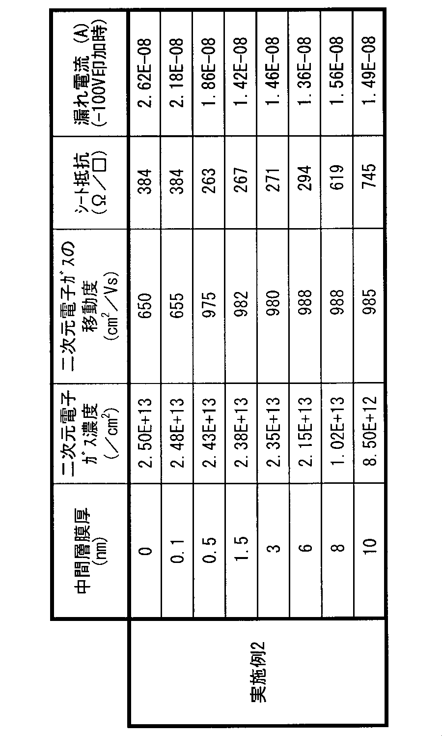
表2に示すように、中間層6aの厚みが0.5nm以上の場合、中間層6aを設けない場合に比して、二次元電子ガスの移動度が高い値となっている。また、中間層6aの厚みが6nm以下の場合であれば、二次元電子ガス濃度の値が中間層6aを設けない場合と同程度となっている。さらには、中間層6aの厚みが0.5nm以上6nm以下の場合であれば、シート抵抗の値が、中間層6aを設けない場合に比して低い300Ω/□以下の値に保たれている。
一方で、表2に示すように、いずれのHEMT素子についても、漏れ電流の値は、表1に示した比較例1の場合(ゲート電極が同じNi/Auの場合)の1/1000以下にまで低減されている。
以上のことから、キャップ層6bと障壁層5との間に中間層6aを0.5nm以上の厚みに形成することで、漏れ電流が低減されているとともに、二次元電子ガスの移動度が高いHEMT素子が実現されることがわかる。さらに、中間層6aの厚みを6nm以下とすることで、二次元電子ガス濃度が高く、かつシート抵抗が小さいHEMT素子が実現されることがわかる。
Claims (26)
- 下地基板の上にIII族窒化物層群を(0001)結晶面が基板面に対し略平行となるよう積層形成したエピタキシャル基板と、
ショットキー性電極と、
を備える半導体素子であって、
前記エピタキシャル基板が、
Inx1Aly1Gaz1N(x1+y1+z1=1、z1>0)なる組成の第1のIII族窒化物からなるチャネル層と、
Inx2Aly2N(x2+y2=1、x2>0、y2>0)なる組成の第2のIII族窒化物からなる障壁層と、
GaNからなり前記障壁層に隣接する中間層と、
AlNからなり前記中間層に隣接するキャップ層と、
を備え、
前記ショットキー性電極が前記キャップ層に接合されてなる、
ことを特徴とする半導体素子。 - 請求項1に記載の半導体素子であって、
前記中間層の膜厚が0.5nm以上である、
ことを特徴とする半導体素子。 - 請求項2に記載の半導体素子であって、
前記中間層の膜厚が6nm以下である、
ことを特徴とする半導体素子。 - 請求項1ないし請求項3のいずれかに記載の半導体素子であって、
前記キャップ層の膜厚が0.5nm以上6nm以下である、
ことを特徴とする半導体素子。 - 請求項1ないし請求項4のいずれかに記載の半導体素子であって、
前記第2のIII族窒化物のバンドギャップが前記第1のIII族窒化物のバンドギャップよりも大きい、
ことを特徴とする半導体素子。 - 請求項1ないし請求項5のいずれかに記載の半導体素子であって、
前記ショットキー性電極がNi、Pt、Pd、Auの少なくとも1つを含んでなる、
ことを特徴とする半導体素子。 - 請求項1ないし請求項6のいずれかに記載の半導体素子であって、
前記キャップ層の自乗平均表面粗さが0.5nm以下である、
ことを特徴とする半導体素子。 - 請求項1ないし請求項7のいずれかに記載の半導体素子であって、
前記第2のIII族窒化物が、Inx2Aly2N(x2+y2=1、0.14≦x2≦0.24)である、
ことを特徴とする半導体素子。 - 請求項1ないし請求項8のいずれかに記載の半導体素子であって、
前記第1のIII族窒化物がAly1Gaz1N(y1+z1=1、z1>0)である、
ことを特徴とする半導体素子。 - 請求項9に記載の半導体素子であって、
前記第1のIII族窒化物がGaNである、
ことを特徴とする半導体素子。 - 請求項9または請求項10に記載の半導体素子であって、
前記チャネル層と前記障壁層との間に、Inx3Aly3Gaz3N(x3+y3+z3=1、y3>0)なる組成を有し、前記第2のIII族窒化物よりもバンドギャップが大きい第3のIII族窒化物からなるスペーサ層をさらに備える、
ことを特徴とする半導体素子。 - 請求項11に記載の半導体素子であって、
前記第3のIII族窒化物がAlNである、
ことを特徴とする半導体素子。 - 請求項1ないし請求項12のいずれかに記載の半導体素子であって、
オーミック性電極が前記ショットキー性電極と同一の前記キャップ層に接合されてなる、
ことを特徴とする半導体素子。 - 請求項13に記載の半導体素子であるHEMT素子であって、
前記ショットキー性電極がゲート電極であり、前記オーミック性電極がソース電極およびドレイン電極である、
ことを特徴とするHEMT素子。 - 下地基板の上にIII族窒化物層群を(0001)結晶面が基板面に対し略平行となるよう積層形成したエピタキシャル基板と、
ショットキー性電極と、
を備える半導体素子の製造方法であって、
下地基板の上に、Inx1Aly1Gaz1N(x1+y1+z1=1、z1>0)なる組成の第1のIII族窒化物にてチャネル層を形成するチャネル層形成工程と、
前記チャネル層の上に、Inx2Aly2N(x2+y2=1、x2>0、y2>0)なる組成の第2のIII族窒化物にて障壁層を形成する障壁層形成工程と、
GaNにて中間層を前記障壁層に隣接形成する中間層形成工程と、
AlNにてキャップ層を前記中間層に隣接形成するキャップ層形成工程と、
前記キャップ層にショットキー性電極を接合形成するショットキー性電極形成工程と、
を備えることを特徴とする半導体素子の製造方法。 - 請求項15に記載の半導体素子の製造方法であって、
前記中間層を0.5nm以上の厚みに形成する、
ことを特徴とする半導体素子の製造方法。 - 請求項16に記載の半導体素子の製造方法であって、
前記中間層を6nm以下の厚みに形成する、
ことを特徴とする半導体素子の製造方法。 - 請求項15ないし請求項17のいずれかに記載の半導体素子の製造方法であって、
前記キャップ層を0.5nm以上6nm以下の厚みに形成する、
ことを特徴とする半導体素子の製造方法。 - 請求項15ないし請求項18のいずれかに記載の半導体素子の製造方法であって、
前記第2のIII族窒化物のバンドギャップが前記第1のIII族窒化物のバンドギャップよりも大きい、
ことを特徴とする半導体素子の製造方法。 - 請求項15ないし請求項19のいずれかに記載の半導体素子の製造方法であって、
前記ショットキー性電極形成工程においては、前記ショットキー性電極をNi、Pt、Pd、Auの少なくとも1つを含むように形成する、
ことを特徴とする半導体素子の製造方法。 - 請求項15ないし請求項20のいずれかに記載の半導体素子の製造方法であって、
前記第2のIII族窒化物が、Inx2Aly2N(x2+y2=1、0.14≦x2≦0.24)である、
ことを特徴とする半導体素子の製造方法。 - 請求項15ないし請求項21のいずれかに記載の半導体素子の製造方法であって、
前記第1のIII族窒化物がAly1Gaz1N(y1+z1=1、z1>0)である、
ことを特徴とする半導体素子の製造方法。 - 請求項22に記載の半導体素子の製造方法であって、
前記第1のIII族窒化物がGaNである、
ことを特徴とする半導体素子の製造方法。 - 請求項22または請求項23に記載の半導体素子の製造方法であって、
前記チャネル層と前記障壁層との間に、Inx3Aly3Gaz3N(x3+y3+z3=1、y3>0)なる組成を有し、前記第2のIII族窒化物よりもバンドギャップが大きい第3のIII族窒化物にてスペーサ層を形成するスペーサ層形成工程、
をさらに備えることを特徴とする半導体素子の製造方法。 - 請求項24に記載の半導体素子の製造方法であって、
前記第3のIII族窒化物がAlNである、
ことを特徴とする半導体素子の製造方法。 - 請求項15ないし請求項25のいずれかに記載の半導体素子の製造方法であって、
前記ショットキー性電極が形成される前記キャップ層にオーミック性電極を接合形成するオーミック性電極形成工程、
をさらに備えることを特徴とする半導体素子の製造方法。
Priority Applications (5)
| Application Number | Priority Date | Filing Date | Title |
|---|---|---|---|
| EP12842688.9A EP2720257A4 (en) | 2012-08-10 | 2012-08-10 | SEMICONDUCTOR DEVICE, HEMT DEVICE AND METHOD FOR PRODUCING THE SEMICONDUCTOR DEVICE |
| CN201280003274.5A CN103828030B (zh) | 2012-08-10 | 2012-08-10 | 半导体元件、hemt元件、以及半导体元件的制造方法 |
| PCT/JP2012/070521 WO2014024310A1 (ja) | 2012-08-10 | 2012-08-10 | 半導体素子、hemt素子、および半導体素子の製造方法 |
| KR1020137010864A KR101933230B1 (ko) | 2012-08-10 | 2012-08-10 | 반도체 소자, hemt 소자, 및 반도체 소자의 제조 방법 |
| US13/855,148 US9478650B2 (en) | 2012-08-10 | 2013-04-02 | Semiconductor device, HEMT device, and method of manufacturing semiconductor device |
Applications Claiming Priority (1)
| Application Number | Priority Date | Filing Date | Title |
|---|---|---|---|
| PCT/JP2012/070521 WO2014024310A1 (ja) | 2012-08-10 | 2012-08-10 | 半導体素子、hemt素子、および半導体素子の製造方法 |
Related Child Applications (1)
| Application Number | Title | Priority Date | Filing Date |
|---|---|---|---|
| US13/855,148 Continuation US9478650B2 (en) | 2012-08-10 | 2013-04-02 | Semiconductor device, HEMT device, and method of manufacturing semiconductor device |
Publications (1)
| Publication Number | Publication Date |
|---|---|
| WO2014024310A1 true WO2014024310A1 (ja) | 2014-02-13 |
Family
ID=50065536
Family Applications (1)
| Application Number | Title | Priority Date | Filing Date |
|---|---|---|---|
| PCT/JP2012/070521 Ceased WO2014024310A1 (ja) | 2012-08-10 | 2012-08-10 | 半導体素子、hemt素子、および半導体素子の製造方法 |
Country Status (5)
| Country | Link |
|---|---|
| US (1) | US9478650B2 (ja) |
| EP (1) | EP2720257A4 (ja) |
| KR (1) | KR101933230B1 (ja) |
| CN (1) | CN103828030B (ja) |
| WO (1) | WO2014024310A1 (ja) |
Cited By (1)
| Publication number | Priority date | Publication date | Assignee | Title |
|---|---|---|---|---|
| WO2016158785A1 (ja) * | 2015-03-29 | 2016-10-06 | 住友化学株式会社 | 積層基板の測定方法、積層基板および測定装置 |
Families Citing this family (10)
| Publication number | Priority date | Publication date | Assignee | Title |
|---|---|---|---|---|
| WO2015068448A1 (ja) * | 2013-11-06 | 2015-05-14 | シャープ株式会社 | 窒化物半導体 |
| JP6149786B2 (ja) * | 2014-04-11 | 2017-06-21 | 豊田合成株式会社 | 半導体装置および半導体装置の製造方法 |
| JP6792135B2 (ja) * | 2015-10-30 | 2020-11-25 | 富士通株式会社 | 化合物半導体装置及びその製造方法 |
| CN105576031A (zh) * | 2015-12-30 | 2016-05-11 | 东莞市青麦田数码科技有限公司 | 一种以GaN为界面层的GaAs沟道MOS界面结构 |
| CN106601787B (zh) * | 2016-12-01 | 2020-06-26 | 北京大学 | 一种InxAlyGa1-x-yN/GaN异质结构及其外延方法 |
| CN108573853B (zh) * | 2017-03-09 | 2021-01-29 | 合肥彩虹蓝光科技有限公司 | 一种GaN基HEMT器件外延结构及其生长方法 |
| CN108682625A (zh) * | 2018-05-22 | 2018-10-19 | 西安电子科技大学 | 基于场板和P型GaN帽层的RESURF GaN基肖特基势垒二极管 |
| JP7439536B2 (ja) * | 2020-01-28 | 2024-02-28 | 富士通株式会社 | 半導体装置 |
| CN112736131B (zh) * | 2021-01-05 | 2023-02-10 | 西安电子科技大学 | YAlN/GaN高电子迁移率晶体管及其制作方法 |
| CN117239001A (zh) * | 2023-11-13 | 2023-12-15 | 合肥美镓传感科技有限公司 | 光电探测器及其制备方法、检测方法、光电探测器阵列 |
Citations (4)
| Publication number | Priority date | Publication date | Assignee | Title |
|---|---|---|---|---|
| JP2000294768A (ja) * | 1999-04-01 | 2000-10-20 | Sony Corp | 半導体素子およびその製造方法 |
| JP2007103778A (ja) * | 2005-10-06 | 2007-04-19 | Mitsubishi Electric Corp | 電界効果型トランジスタ |
| WO2012014675A1 (ja) * | 2010-07-29 | 2012-02-02 | 日本碍子株式会社 | 半導体素子、hemt素子、および半導体素子の製造方法 |
| JP2012119638A (ja) * | 2010-12-03 | 2012-06-21 | Fujitsu Ltd | 化合物半導体装置及びその製造方法 |
Family Cites Families (32)
| Publication number | Priority date | Publication date | Assignee | Title |
|---|---|---|---|---|
| JP3209270B2 (ja) * | 1999-01-29 | 2001-09-17 | 日本電気株式会社 | ヘテロ接合電界効果トランジスタ |
| US6495894B2 (en) * | 2000-05-22 | 2002-12-17 | Ngk Insulators, Ltd. | Photonic device, a substrate for fabricating a photonic device, a method for fabricating the photonic device and a method for manufacturing the photonic device-fabricating substrate |
| JP4001262B2 (ja) * | 2001-02-27 | 2007-10-31 | 日本碍子株式会社 | 窒化物膜の製造方法 |
| JP4179539B2 (ja) * | 2003-01-15 | 2008-11-12 | 富士通株式会社 | 化合物半導体装置及びその製造方法 |
| JP4727169B2 (ja) * | 2003-08-04 | 2011-07-20 | 日本碍子株式会社 | エピタキシャル基板、当該エピタキシャル基板の製造方法、当該エピタキシャル基板の反り抑制方法、および当該エピタキシャル基板を用いた半導体積層構造 |
| EP2273553B1 (en) * | 2004-06-30 | 2020-02-12 | IMEC vzw | A method for fabricating AlGaN/GaN HEMT devices |
| US7709859B2 (en) | 2004-11-23 | 2010-05-04 | Cree, Inc. | Cap layers including aluminum nitride for nitride-based transistors |
| US7253454B2 (en) * | 2005-03-03 | 2007-08-07 | Cree, Inc. | High electron mobility transistor |
| JP2006295126A (ja) * | 2005-03-15 | 2006-10-26 | Sumitomo Electric Ind Ltd | Iii族窒化物半導体素子およびエピタキシャル基板 |
| JP4462330B2 (ja) * | 2007-11-02 | 2010-05-12 | 住友電気工業株式会社 | Iii族窒化物電子デバイス |
| EP3067921B1 (en) * | 2008-03-24 | 2020-08-26 | NGK Insulators, Ltd. | Process for producing an epitaxial substrate for a semiconductor element |
| CN101981658B (zh) * | 2008-03-24 | 2014-10-29 | 日本碍子株式会社 | 半导体元件、半导体元件用外延基板及其制作方法 |
| JP5465469B2 (ja) * | 2008-09-04 | 2014-04-09 | 日本碍子株式会社 | エピタキシャル基板、半導体デバイス基板、およびhemt素子 |
| JP4677499B2 (ja) * | 2008-12-15 | 2011-04-27 | Dowaエレクトロニクス株式会社 | 電子デバイス用エピタキシャル基板およびその製造方法 |
| WO2010151721A1 (en) | 2009-06-25 | 2010-12-29 | The Government Of The United States Of America, As Represented By The Secretary Of The Navy | Transistor with enhanced channel charge inducing material layer and threshold voltage control |
| JP5702058B2 (ja) * | 2009-08-28 | 2015-04-15 | 日本碍子株式会社 | 半導体素子用エピタキシャル基板、半導体素子、および、半導体素子用エピタキシャル基板の作製方法 |
| JP5580009B2 (ja) * | 2009-08-28 | 2014-08-27 | 日本碍子株式会社 | 半導体素子用エピタキシャル基板、半導体素子、および、半導体素子用エピタキシャル基板の作製方法 |
| DE102009041548A1 (de) * | 2009-09-15 | 2011-03-24 | Fraunhofer-Gesellschaft zur Förderung der angewandten Forschung e.V. | Halbleiterstruktur |
| JP5308290B2 (ja) * | 2009-09-15 | 2013-10-09 | 日本碍子株式会社 | 半導体素子用エピタキシャル基板、ショットキー接合構造、およびショットキー接合構造の漏れ電流抑制方法 |
| EP2498282A4 (en) * | 2009-11-04 | 2014-06-25 | Dowa Electronics Materials Co Ltd | EPITACTIC COATED GROUP III NITRIDE SUBSTRATE |
| JP5524235B2 (ja) * | 2009-11-06 | 2014-06-18 | 日本碍子株式会社 | 半導体素子用エピタキシャル基板および半導体素子用エピタキシャル基板の製造方法 |
| WO2011102045A1 (ja) * | 2010-02-16 | 2011-08-25 | 日本碍子株式会社 | エピタキシャル基板およびエピタキシャル基板の製造方法 |
| EP2555232A4 (en) * | 2010-03-24 | 2014-12-10 | Ngk Insulators Ltd | EPITACTICAL SUBSTRATE FOR A SEMICONDUCTOR ELEMENT AND SEMICONDUCTOR ELEMENT |
| CN102859653A (zh) * | 2010-04-28 | 2013-01-02 | 日本碍子株式会社 | 外延基板以及外延基板的制造方法 |
| EP2600394B1 (en) * | 2010-07-29 | 2017-12-27 | NGK Insulators, Ltd. | Epitaxial substrate for semiconductor element and production method thereof |
| EP2610898B1 (en) * | 2010-08-25 | 2020-11-25 | NGK Insulators, Ltd. | Method for fabricating epitaxial substrate for semiconductor device, and method for fabricating semiconductor device |
| US8895993B2 (en) * | 2011-01-31 | 2014-11-25 | Taiwan Semiconductor Manufacturing Company, Ltd. | Low gate-leakage structure and method for gallium nitride enhancement mode transistor |
| JP5776217B2 (ja) * | 2011-02-24 | 2015-09-09 | 富士通株式会社 | 化合物半導体装置 |
| US8710511B2 (en) * | 2011-07-29 | 2014-04-29 | Northrop Grumman Systems Corporation | AIN buffer N-polar GaN HEMT profile |
| JP5117609B1 (ja) * | 2011-10-11 | 2013-01-16 | 株式会社東芝 | 窒化物半導体ウェーハ、窒化物半導体装置及び窒化物半導体結晶の成長方法 |
| US9165766B2 (en) * | 2012-02-03 | 2015-10-20 | Transphorm Inc. | Buffer layer structures suited for III-nitride devices with foreign substrates |
| EP2667415B1 (en) * | 2012-05-22 | 2021-02-17 | Nexperia B.V. | Heterojunction semiconductor device and manufacturing method |
-
2012
- 2012-08-10 CN CN201280003274.5A patent/CN103828030B/zh not_active Expired - Fee Related
- 2012-08-10 WO PCT/JP2012/070521 patent/WO2014024310A1/ja not_active Ceased
- 2012-08-10 KR KR1020137010864A patent/KR101933230B1/ko not_active Expired - Fee Related
- 2012-08-10 EP EP12842688.9A patent/EP2720257A4/en not_active Ceased
-
2013
- 2013-04-02 US US13/855,148 patent/US9478650B2/en not_active Expired - Fee Related
Patent Citations (4)
| Publication number | Priority date | Publication date | Assignee | Title |
|---|---|---|---|---|
| JP2000294768A (ja) * | 1999-04-01 | 2000-10-20 | Sony Corp | 半導体素子およびその製造方法 |
| JP2007103778A (ja) * | 2005-10-06 | 2007-04-19 | Mitsubishi Electric Corp | 電界効果型トランジスタ |
| WO2012014675A1 (ja) * | 2010-07-29 | 2012-02-02 | 日本碍子株式会社 | 半導体素子、hemt素子、および半導体素子の製造方法 |
| JP2012119638A (ja) * | 2010-12-03 | 2012-06-21 | Fujitsu Ltd | 化合物半導体装置及びその製造方法 |
Non-Patent Citations (4)
| Title |
|---|
| F. MEDJDOUB; J.-F. CARLIN; M. GONSCHOREK; E. FELTIN; M.A. PY; D. DUCATTEAU; C. GAQUIERE; N. GRANDJEAN; E. KOHN: "Can InAN/GaN be an alternative to high power/high temperature AlGaN/GaN devices?", IEEE IEDM TECH. DIGEST IN IEEE IEDM, 2006, pages 673 |
| See also references of EP2720257A4 |
| STACIA KELLER; YI-FENG WU; GIACINTA PARISH; NAIQIAN ZIANG; JANE J. XU; BERND P. KELLER; STEVEN P. DENBAARS; UMESH K. MISHRA: "Gallium Nitride Based High Power Heterojunction Field Effect Transistors: process Development and Present Status at USCB", IEEE TRANS. ELECTRON DEVICES, vol. 48, 2001, pages 552, XP011017534 |
| TOSHIHIDE KIKKAWA: "Highly Reliable 250W High Electron Mobility Transistor Power Amplifier", JPN. J. APPL. PHYS., vol. 44, 2005, pages 4896, XP001502263, DOI: doi:10.1143/JJAP.44.4896 |
Cited By (3)
| Publication number | Priority date | Publication date | Assignee | Title |
|---|---|---|---|---|
| WO2016158785A1 (ja) * | 2015-03-29 | 2016-10-06 | 住友化学株式会社 | 積層基板の測定方法、積層基板および測定装置 |
| JPWO2016158785A1 (ja) * | 2015-03-29 | 2018-01-18 | 住友化学株式会社 | 積層基板の測定方法、積層基板および測定装置 |
| US10222321B2 (en) | 2015-03-29 | 2019-03-05 | Sumitomo Chemical Company, Limited | Laminate substrate measurement method, laminate substrate and measurement apparatus |
Also Published As
| Publication number | Publication date |
|---|---|
| US20140042451A1 (en) | 2014-02-13 |
| CN103828030A (zh) | 2014-05-28 |
| CN103828030B (zh) | 2017-11-10 |
| EP2720257A1 (en) | 2014-04-16 |
| KR20150043182A (ko) | 2015-04-22 |
| US9478650B2 (en) | 2016-10-25 |
| EP2720257A4 (en) | 2015-09-23 |
| KR101933230B1 (ko) | 2018-12-27 |
Similar Documents
| Publication | Publication Date | Title |
|---|---|---|
| CN103828030B (zh) | 半导体元件、hemt元件、以及半导体元件的制造方法 | |
| JP5782033B2 (ja) | 半導体素子用エピタキシャル基板、半導体素子、pn接合ダイオード素子、および半導体素子用エピタキシャル基板の製造方法 | |
| JP5634681B2 (ja) | 半導体素子 | |
| JP6170893B2 (ja) | 半導体素子用エピタキシャル基板の作製方法 | |
| CN103081080B (zh) | 半导体元件用外延基板、半导体元件、半导体元件用外延基板的制作方法、以及半导体元件的制作方法 | |
| JP5758880B2 (ja) | 半導体素子用エピタキシャル基板、半導体素子、および半導体素子用エピタキシャル基板の作製方法 | |
| JP5580009B2 (ja) | 半導体素子用エピタキシャル基板、半導体素子、および、半導体素子用エピタキシャル基板の作製方法 | |
| JP5562579B2 (ja) | 半導体素子用エピタキシャル基板の作製方法 | |
| JP2014053639A (ja) | 半導体素子用エピタキシャル基板の作製方法 | |
| US20120168771A1 (en) | Semiconductor element, hemt element, and method of manufacturing semiconductor element | |
| US10332975B2 (en) | Epitaxial substrate for semiconductor device and method for manufacturing same | |
| JP5308290B2 (ja) | 半導体素子用エピタキシャル基板、ショットキー接合構造、およびショットキー接合構造の漏れ電流抑制方法 | |
| JP5806545B2 (ja) | 半導体素子、hemt素子、および半導体素子の製造方法 | |
| JP2012186268A (ja) | エピタキシャル基板 | |
| JP2016167473A (ja) | 窒化物半導体積層基板、窒化物半導体装置および窒化物半導体積層基板の製造方法 |
Legal Events
| Date | Code | Title | Description |
|---|---|---|---|
| ENP | Entry into the national phase |
Ref document number: 20137010864 Country of ref document: KR Kind code of ref document: A |
|
| WWE | Wipo information: entry into national phase |
Ref document number: 2012842688 Country of ref document: EP |
|
| 121 | Ep: the epo has been informed by wipo that ep was designated in this application |
Ref document number: 12842688 Country of ref document: EP Kind code of ref document: A1 |
|
| NENP | Non-entry into the national phase |
Ref country code: DE |
|
| NENP | Non-entry into the national phase |
Ref country code: JP |