WO2014030412A1 - 化合物太陽電池およびその製造方法 - Google Patents
化合物太陽電池およびその製造方法 Download PDFInfo
- Publication number
- WO2014030412A1 WO2014030412A1 PCT/JP2013/066638 JP2013066638W WO2014030412A1 WO 2014030412 A1 WO2014030412 A1 WO 2014030412A1 JP 2013066638 W JP2013066638 W JP 2013066638W WO 2014030412 A1 WO2014030412 A1 WO 2014030412A1
- Authority
- WO
- WIPO (PCT)
- Prior art keywords
- layer
- light absorption
- solar cell
- compound
- substrate
- Prior art date
- Legal status (The legal status is an assumption and is not a legal conclusion. Google has not performed a legal analysis and makes no representation as to the accuracy of the status listed.)
- Ceased
Links
Images


Classifications
-
- H—ELECTRICITY
- H10—SEMICONDUCTOR DEVICES; ELECTRIC SOLID-STATE DEVICES NOT OTHERWISE PROVIDED FOR
- H10F—INORGANIC SEMICONDUCTOR DEVICES SENSITIVE TO INFRARED RADIATION, LIGHT, ELECTROMAGNETIC RADIATION OF SHORTER WAVELENGTH OR CORPUSCULAR RADIATION
- H10F77/00—Constructional details of devices covered by this subclass
- H10F77/10—Semiconductor bodies
- H10F77/12—Active materials
- H10F77/126—Active materials comprising only Group I-III-VI chalcopyrite materials, e.g. CuInSe2, CuGaSe2 or CuInGaSe2 [CIGS]
-
- H—ELECTRICITY
- H10—SEMICONDUCTOR DEVICES; ELECTRIC SOLID-STATE DEVICES NOT OTHERWISE PROVIDED FOR
- H10F—INORGANIC SEMICONDUCTOR DEVICES SENSITIVE TO INFRARED RADIATION, LIGHT, ELECTROMAGNETIC RADIATION OF SHORTER WAVELENGTH OR CORPUSCULAR RADIATION
- H10F10/00—Individual photovoltaic cells, e.g. solar cells
- H10F10/10—Individual photovoltaic cells, e.g. solar cells having potential barriers
- H10F10/16—Photovoltaic cells having only PN heterojunction potential barriers
- H10F10/167—Photovoltaic cells having only PN heterojunction potential barriers comprising Group I-III-VI materials, e.g. CdS/CuInSe2 [CIS] heterojunction photovoltaic cells
-
- H—ELECTRICITY
- H10—SEMICONDUCTOR DEVICES; ELECTRIC SOLID-STATE DEVICES NOT OTHERWISE PROVIDED FOR
- H10F—INORGANIC SEMICONDUCTOR DEVICES SENSITIVE TO INFRARED RADIATION, LIGHT, ELECTROMAGNETIC RADIATION OF SHORTER WAVELENGTH OR CORPUSCULAR RADIATION
- H10F71/00—Manufacture or treatment of devices covered by this subclass
-
- Y—GENERAL TAGGING OF NEW TECHNOLOGICAL DEVELOPMENTS; GENERAL TAGGING OF CROSS-SECTIONAL TECHNOLOGIES SPANNING OVER SEVERAL SECTIONS OF THE IPC; TECHNICAL SUBJECTS COVERED BY FORMER USPC CROSS-REFERENCE ART COLLECTIONS [XRACs] AND DIGESTS
- Y02—TECHNOLOGIES OR APPLICATIONS FOR MITIGATION OR ADAPTATION AGAINST CLIMATE CHANGE
- Y02E—REDUCTION OF GREENHOUSE GAS [GHG] EMISSIONS, RELATED TO ENERGY GENERATION, TRANSMISSION OR DISTRIBUTION
- Y02E10/00—Energy generation through renewable energy sources
- Y02E10/50—Photovoltaic [PV] energy
- Y02E10/541—CuInSe2 material PV cells
-
- Y—GENERAL TAGGING OF NEW TECHNOLOGICAL DEVELOPMENTS; GENERAL TAGGING OF CROSS-SECTIONAL TECHNOLOGIES SPANNING OVER SEVERAL SECTIONS OF THE IPC; TECHNICAL SUBJECTS COVERED BY FORMER USPC CROSS-REFERENCE ART COLLECTIONS [XRACs] AND DIGESTS
- Y02—TECHNOLOGIES OR APPLICATIONS FOR MITIGATION OR ADAPTATION AGAINST CLIMATE CHANGE
- Y02P—CLIMATE CHANGE MITIGATION TECHNOLOGIES IN THE PRODUCTION OR PROCESSING OF GOODS
- Y02P70/00—Climate change mitigation technologies in the production process for final industrial or consumer products
- Y02P70/50—Manufacturing or production processes characterised by the final manufactured product
Definitions
- the present invention relates to CuInSe 2 (CIS) composed of Group I, Group III and Group VI elements, or a Cu (In, Ga) Se 2 (CIGS) compound semiconductor (Group I-III-VI) in which Ga is dissolved.
- the present invention relates to a compound solar cell having a high light conversion efficiency (hereinafter referred to as “conversion efficiency”) using a compound semiconductor) for a light absorption layer and a method for efficiently producing the compound solar cell.
- a compound solar cell using a CIS or CIGS (hereinafter referred to as “CIGS-based”) compound semiconductor for a light absorption layer has a high conversion efficiency and can be formed into a thin film, and has a conversion efficiency due to light irradiation or the like. It is known to have the advantage of less degradation.
- the conduction band difference ⁇ Ec between the light absorption layer and the buffer layer is set to 0 ⁇ ⁇ Ec ⁇ 0.4, carrier recombination in the vicinity of the interface between the light absorption layer and the buffer layer can be effectively suppressed, It is known that high conversion efficiency can be obtained (see Non-Patent Document 1).
- the buffer layer having a conduction band satisfying the above conditions is Zn (O, S, OH), In (S, OH), (Zn, Mg). Examples thereof include those composed of mixed crystals such as O.
- the composition of the CIGS compound semiconductor with high photoelectric conversion efficiency is currently in the range of 0.2 ⁇ Ga / (In + Ga) ⁇ 0.5 when attention is paid to the ratio of Ga to In.
- the ZnS ratio and MgO ratio to ZnO and the InO ratio to InS are increased.
- the InO ratio is increased, the crystal orientation tends to be random.
- the present invention has been made in view of the above problems, and can be manufactured by continuously performing the subsequent steps without taking out the buffer layer under the atmosphere, and having high conversion efficiency. It is an object of the present invention to provide a battery and a manufacturing method thereof.
- a compound solar cell comprising a compound light absorption layer made of an I-III-VI group compound semiconductor, a buffer layer, and a surface electrode layer on a substrate, the compound light absorption
- a method for producing a compound solar cell according to the first aspect wherein a compound light absorption layer comprising an I-III-VI group compound semiconductor is formed on a substrate while the long substrate is running in the longitudinal direction.
- a compound solar cell comprising: a step of forming an interface layer; a step of forming an interface layer; a step of forming a buffer layer; and a step of forming a surface electrode layer.
- the manufacturing method is the second gist.
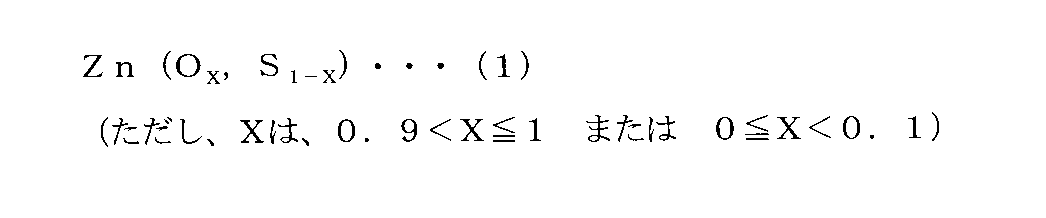
- an interface layer made of a mixed crystal having the composition represented by the general formula (1) is provided between the compound light absorption layer and the buffer layer.
- the compound light absorption layer is in contact with the interface layer made of a mixed crystal having a relatively uniform crystal orientation in a direction perpendicular to the surface of the compound light absorption layer, so that a lattice is formed at the interface between the compound light absorption layer and the interface layer. Defects are unlikely to occur, carrier recombination is effectively suppressed, and a decrease in conversion efficiency is prevented.
- the buffer layer is formed on the interface layer crystallized in the direction perpendicular to the surface of the compound light absorption layer, the crystals are easily aligned in the direction perpendicular to the surface of the compound light absorption layer due to the influence of the crystal orientation of the interface layer. For this reason, electrons generated in the light absorption layer easily reach the surface electrode layer, and recombination is suppressed.
- the compound solar cell of the present invention uses an I-III-VI group compound semiconductor as the compound light absorption layer, and since high conversion efficiency can be obtained with a thin film, reduction in conversion efficiency is prevented, Has excellent properties.
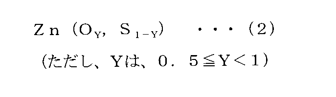
- the buffer layer is a mixed crystal having a composition represented by the following general formula (2)
- the buffer layer is formed transparent in the visible light region, and light absorption loss in the buffer layer can be eliminated. Efficiency can be increased.
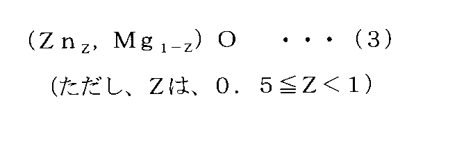
- the buffer layer is a mixed crystal having a composition represented by the following general formula (3)
- the buffer layer is formed transparent in the visible light region, and light absorption loss in the buffer layer can be eliminated. Conversion efficiency can be increased.
- a method for producing a compound solar cell according to the first aspect of the present invention which is a compound comprising an I-III-VI group compound semiconductor on a substrate while the long substrate is running in the longitudinal direction.
- a compound comprising a step of forming a light absorption layer, a step of forming an interface layer, a step of forming a buffer layer, and a step of forming a surface electrode layer, and performing each step continuously in this order under vacuum
- FIG. 1 is a cross-sectional view of a CIGS solar cell according to an embodiment of the present invention.
- This CIGS solar cell includes a substrate 1, a back electrode layer 2, a CIGS light absorption layer (compound light absorption layer) 3, a buffer layer 5, and a surface electrode layer 6 in this order.
- the interface layer 4 made of a mixed crystal having the composition shown in the following general formula (1) is provided between the absorption layer 3 and the buffer layer 5.
- each layer will be described in detail.
- the thickness, size, appearance, and the like of each layer are schematically shown, and are different from actual ones (the same applies to the following drawings).
- the substrate 1 is used as a support substrate, and an appropriate substrate is selected from a glass substrate, a metal substrate, a resin substrate, and the like according to the purpose and design needs.
- a glass substrate low alkali glass (high strain point glass) having a very low alkali metal element content, alkali-free glass not containing an alkali metal element, blue plate glass, and the like are preferably used.
- blue glass it is preferable to use blue glass as the substrate 1 because the alkali metal element diffuses from the substrate 1 to the CIGS light absorption layer 3 and the solar cell characteristics are improved.
- the substrate 1 is long and flexible because CIGS solar cells can be manufactured by a roll-to-roll method or a stepping roll method.
- the “elongate” means that the length in the length direction is 10 times or more the length in the width direction, and more preferably 30 times or more.
- the thickness of the substrate 1 is preferably in the range of 5 to 200 ⁇ m, more preferably in the range of 10 to 100 ⁇ m. That is, if the thickness is too thick, the flexibility of the CIGS solar cell is lost, the stress applied when the CIGS solar cell is bent increases, and the laminated structure such as the CIGS light absorption layer 3 may be damaged. This is because if the substrate is too thin, the substrate 1 is buckled when the CIGS solar cell is manufactured, and the product defect rate of the CIGS solar cell tends to increase.
- the back electrode layer 2 formed on the substrate 1 is formed in a single layer or multiple layers by, for example, molybdenum (Mo), tungsten (W), chromium (Cr), titanium (Ti) or the like.
- the thickness of the back electrode layer 2 (in the case of multiple layers, the total thickness of each layer) is preferably in the range of 10 to 1000 ⁇ m. However, when the substrate 1 is conductive and has the function of the back electrode layer 2, the back electrode layer 2 may not be provided.
- a barrier layer (not shown) is provided on the substrate 1 or the back electrode layer 2 for the purpose of preventing this. May be.
- a barrier layer uses, for example, a forming material such as Cr, nickel (Ni), NiCr, cobalt (Co), etc., and a sputtering method, a vapor deposition method, a CVD method, a sol-gel method, a liquid phase deposition method, or the like. Can be formed.
- the CIGS light absorption layer 3 formed on the back electrode layer 2 is a compound semiconductor having a chalcopyrite crystal structure composed of four elements of copper (Cu), indium (In), gallium (Ga), and selenium (Se). Is formed.
- the thickness is preferably in the range of 1.0 to 3.0 ⁇ m, more preferably in the range of 1.5 to 2.5 ⁇ m. If the thickness is too thin, the amount of light absorption when used as the light absorption layer is reduced, and the performance of the solar cell tends to be reduced. Conversely, if it is too thick, the time taken to form the CIGS light absorption layer 3 This is because it tends to increase and productivity tends to be inferior.
- Such a CIGS light absorption layer 3 can be formed by vacuum deposition, selenization / sulfurization, sputtering, or the like.
- the composition ratio of Cu, In, and Ga in the CIGS light absorption layer 3 satisfies the formula 0.7 ⁇ Cu / (Ga + In) ⁇ 0.95 (molar ratio). If this equation is satisfied, it is possible to further prevent Cu (2-X) Se from being excessively taken into the CIGS light absorption layer 3 and to make the entire layer slightly deficient in Cu. Because. Moreover, it is preferable that the ratio of Ga and In which are the same element is in the range of 0.10 ⁇ Ga / (Ga + In) ⁇ 0.40 (molar ratio).
- an interface layer 4 made of a single crystal or a mixed crystal having a composition represented by the following general formula (1) is formed on the CIGS light absorption layer 3 (between the buffer layer 5).
- the interface layer with an increased ratio of ZnO or ZnS is formed in contact with the CIGS light absorption layer 3, the crystal orientation in the vicinity of the interface can be aligned in a certain direction, and the recombination of carriers in the vicinity of the interface It has an excellent characteristic that can be reduced.
- the interface layer 4 (ZnOS film) is a single crystal or a mixed crystal
- ZnO and ZnS have different crystal structures, and their ionic radii and lattice constants are different.
- the interface layer 4 when X is 0.9 ⁇ X ⁇ 1, the interface layer 4 has a large composition ratio of ZnO and takes a wurtzite crystal structure based on ZnO. The difference in ion radius and lattice constant from ZnS does not greatly affect the crystalline state.
- the composition ratio of ZnS is large, and the zinc flash crystal structure based on ZnS is adopted. The effect of the difference is small.
- the buffer layer 5 formed on the interface layer 4 is formed of a mixed crystal of a compound containing a group II or group III element. And it is preferable that it is a high resistance n-type semiconductor so that it can make a pn junction with the said CIGS light absorption layer 3, and what laminated
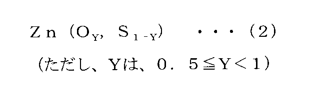
- Zn (O Y , S 1-Y ) (where Y is 0.5 ⁇ Y ⁇ 1)
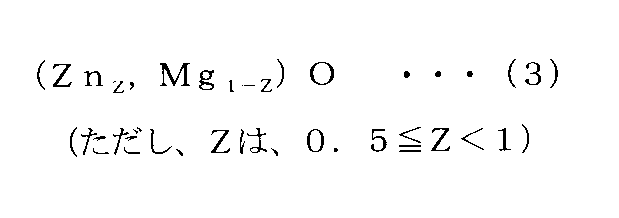
- (Zn Z , Mg 1-Z ) O where Z is 0.5 ⁇ Z ⁇ 1).
- the thickness is preferably in the range of 50 to 200 nm.
- a transparent conductive layer is used as the surface electrode layer 6 formed on the buffer layer 5.
- a material that becomes a thin film with high transmittance and low resistance is preferable, and examples thereof include GZO, ITO, IZO, and zinc aluminum oxide (Al: ZnO).
- the thickness is preferably in the range of 50 to 300 nm.
- the light transmittance of the transparent electrode layer 6 is preferably more than 80%.
- the interface layer 4 having a specific composition is provided between the CIGS light absorption layer 3 and the buffer layer 5, and the interface of the CIGS light absorption layer 3 is provided.
- Lattice defects are less likely to occur and the carrier recombination is effectively suppressed. Therefore, it is possible to sufficiently exhibit excellent performance without impairing high conversion efficiency.
- the CIGS light absorption layer 3 has a chalcopyrite structure and a high conversion efficiency can be realized with a thin film, the solar cell itself can be formed into a thin film. For this reason, the light of the wavelength which is not utilized can be permeate
- the CIGS solar cell can be manufactured, for example, as follows. First, a long substrate 1 is prepared, and a back electrode layer 2, a CIGS light absorption layer 3, an interface layer 4, a buffer layer 5, and a surface electrode layer 6 are continuously formed in this order on the surface by a roll-to-roll method. Can be obtained by stacking. Hereafter, this manufacturing method is demonstrated in detail for every formation process of each layer.
- the back electrode layer 2 is formed on the surface of the long substrate 1 by a roll-to-roll method, using a forming material such as Mo, for example, by sputtering, vapor deposition, ink jet, or the like. .
- the CIGS light absorption layer 3 is formed on the back electrode layer 2 while the substrate 1 on which the back electrode layer 2 is formed is also run by the roll-to-roll method.
- Examples of a method for forming the CIGS light absorption layer 3 include a vacuum deposition method, a selenization / sulfurization method, and a sputtering method.
- the interface layer 4 is formed on the CIGS light absorption layer 3, making the board
- the method for forming the interface layer 4 include a sputtering method and a vapor deposition method.
- a sputtering method is preferably used because it can be easily controlled to a desired composition.
- the sputtering method may be a target sputtering method using a cathode target having a desired composition, or a reactive sputtering method in which chalcogen molecules or compounds such as oxygen and hydrogen sulfide are supplied during sputtering of a Zn material. Other methods may be used.
- the apparatus used for sputtering method can use the opposing target type
- the application to the pair of targets is preferably performed by a high frequency (RF) power source or a direct current (DC) power source is superimposed on the high frequency (RF) power source.
- RF high frequency
- DC direct current
- a virtual center axis ⁇ extending vertically from the layer forming surface of the substrate 1 is assumed, and these two sheets are placed on both sides of the virtual center axis ⁇ .
- the cathode targets 7 and 7 ′ are opposed to each other, and both of them are arranged so as to be substantially V-shaped spreading toward the layer forming surface side (hereinafter referred to as “substrate 1 side”) of the substrate 1. Since the film can be formed with less electric power, the film formation surface and the surface serving as the base thereof are less susceptible to damage, which is preferable.
- the angle ⁇ of at least one of the cathode targets 7 and 7 ′ with respect to the virtual center axis ⁇ is set in the range of 5 to 15 °.
- the back electrode layer 2 and the CIGS light absorption layer 3 formed on the substrate 1 are not shown.
- the buffer layer 5 is formed on the interface layer 4 while the substrate 1 on which the layers up to the interface layer 4 are formed is run in a roll-to-roll manner.
- the method for forming the buffer layer 5 include a solution growth method, a vacuum deposition method, a CVD method, an ALD method, and a sputtering method.
- the sputtering method is preferably used because it is easy to control the composition as desired.
- the cathode targets 7 and 7 ′ are set in a special arrangement as shown in FIG. It is preferable to use an opposed target sputtering apparatus. That is, according to this apparatus, it is possible to form a film with less electric power, and the film forming surface and the surface serving as a base thereof are more unlikely to be damaged.
- the surface electrode layer 6 is formed on the buffer layer 5 while the substrate 1 on which the layers up to the buffer layer 5 are formed is run in a roll-to-roll manner.
- the method for forming the surface electrode layer 6 include a sputtering method, a vapor deposition method, and a metal organic chemical vapor deposition method (MOCVD method).
- the sputtering method is preferably used because it can be easily controlled to the desired composition.
- an opposed target sputtering apparatus set to ## EQU2 ## for the same reason.
- the CIGS solar cell of the present invention can be obtained.
- the base material 1 is once taken out into the atmosphere to form the buffer layer 5, and the surface electrode layer 6 is again formed under vacuum.
- Each process can be performed continuously under vacuum without going through the complicated process of performing.
- the conversion efficiency can be maintained high even though each process is performed continuously, both time reduction and high quality can be realized.
- the above [step of forming the back electrode layer 2] is unnecessary, and the substrate 1 is left as it is. It can be used as a back electrode layer.
- the cathode targets 7 and 7 ′ are not arranged in a substantially V shape spreading toward the substrate 1, but both targets 7 and 7 ′ are arranged in parallel as shown in FIG. May be.
- only one cathode target in this example, the cathode target 7) may be arranged so as to be inclined by an angle ⁇ with respect to the virtual central axis ⁇ .
- the back electrode layer 2, the CIGS light absorption layer 3, the interface layer 4, the buffer layer 5, and the surface electrode layer 6 were formed by the roll-to-roll method. It is not necessary to adopt the method, and it is possible to use a method in which the substrates 1 are prepared and arranged in a single wafer type from the beginning, and the respective layers are sequentially formed thereon. However, production efficiency is good when each layer is formed continuously in a roll-to-roll manner.
- the CIGS light absorption layer 3, the interface layer 4, the buffer layer 5, and the surface electrode layer 6 are continuously arranged in this order under vacuum while the long substrate is running in the longitudinal direction. Therefore, it is preferable because a CIGS solar cell having excellent characteristics at low cost can be obtained.
- Example 1 (Formation of back electrode layer) First, using a magnetron sputtering device (SH-450, ULVAC, Inc.) on the surface of a substrate made of degreased soda lime glass (square shape in plan view with a thickness of 0.55 mm, a width of 20 mm, and a length of 20 mm), discharge gas was used, and a back electrode layer made of Mo having a thickness of 0.8 ⁇ m was formed under the condition of a sputtering rate of 60 nm / min using a direct current (DC) power source so that the sputtering pressure was 1 Pa.
- DC direct current
- a CIGS light absorption layer was formed on the back electrode layer formed as described above. That is, each of Ga, In, Cu, and Se is disposed as a vapor deposition source in a chamber of a vacuum vapor deposition apparatus, the degree of vacuum is 1 ⁇ 10 ⁇ 4 Pa, and the substrate temperature is 250 ° C. , Ga, and Se were simultaneously deposited for 32 minutes. Then, Cu and Se were vapor-deposited simultaneously for 33 minutes while raising the substrate temperature to 550 ° C. at a rate of temperature increase of 20 ° C./min. Finally, In, Ga and Se were vapor-deposited simultaneously while maintaining the substrate temperature at 550 ° C.
- a CIGS light absorption layer was formed on the back electrode layer.
- the vapor deposition sources were heated at temperatures of Ga: 950 ° C., In: 780 ° C., Cu: 1100 ° C., and Se: 140 ° C., respectively.
- the CIGS light absorption layer formed as described above using the counter target sputtering apparatus (the angles ⁇ with respect to the virtual central axis ⁇ is 10 ° each) in which the pair of cathode targets shown in FIG. 2 are arranged in a substantially V shape.
- An interfacial layer was formed on top.
- a cathode target having a composition made of ZnO is used, Ar is used as a discharge gas at the time of sputtering, and a high frequency (RF) power source is used with a power of 100 W and a sputtering pressure of 0.3 Pa.
- RF high frequency
- the above-described counter target sputtering apparatus in which the pair of cathode targets shown in FIG. 2 is arranged in a substantially V shape (the angle ⁇ with respect to the virtual central axis ⁇ is 10 °) is used.
- a buffer layer was formed on the interface layer formed in (1).
- a cathode target having a composition of Zn 0.85 Mg 0.15 O is used, Ar is used as a discharge gas during sputtering, a power density of 0.7 kW / cm 2 and a sputtering pressure of 0 with a radio frequency (RF) power source.
- RF radio frequency
- a surface electrode layer was formed on the buffer layer formed as described above by using a magnetron sputtering apparatus (manufactured by ULVAC, SH-450).
- a magnetron sputtering apparatus manufactured by ULVAC, SH-450.
- As cathode target ITO (In 2 O 3: 90 [atomic%], SnO 2: 10 [atomic%]) was used, the discharge gas Ar and O 2 and (1/10 of Ar flow rate)
- a surface electrode layer made of ITO having a thickness of 200 nm was formed at a sputtering rate of 20 nm / min using a radio frequency (RF) power source so that the sputtering pressure was 0.3 Pa.
- RF radio frequency
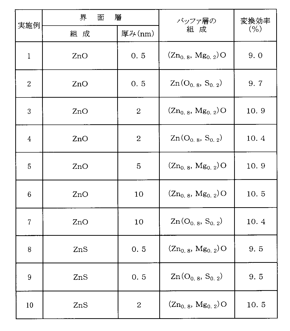
- Examples 2 to 27 A CIGS solar cell was obtained in the same manner as in Example 1 except that the manufacturing conditions were changed as shown in Tables 1 to 3 below.
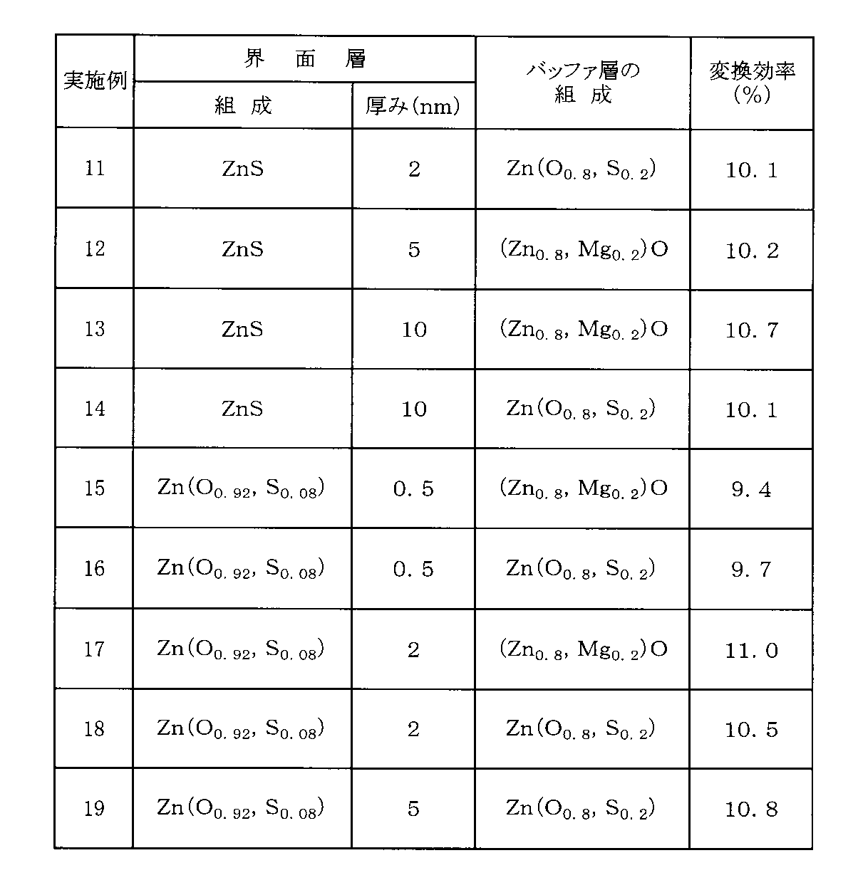
- the CIGS solar cells of Examples 1 to 27 all had excellent conversion efficiency of 9.0% or more.
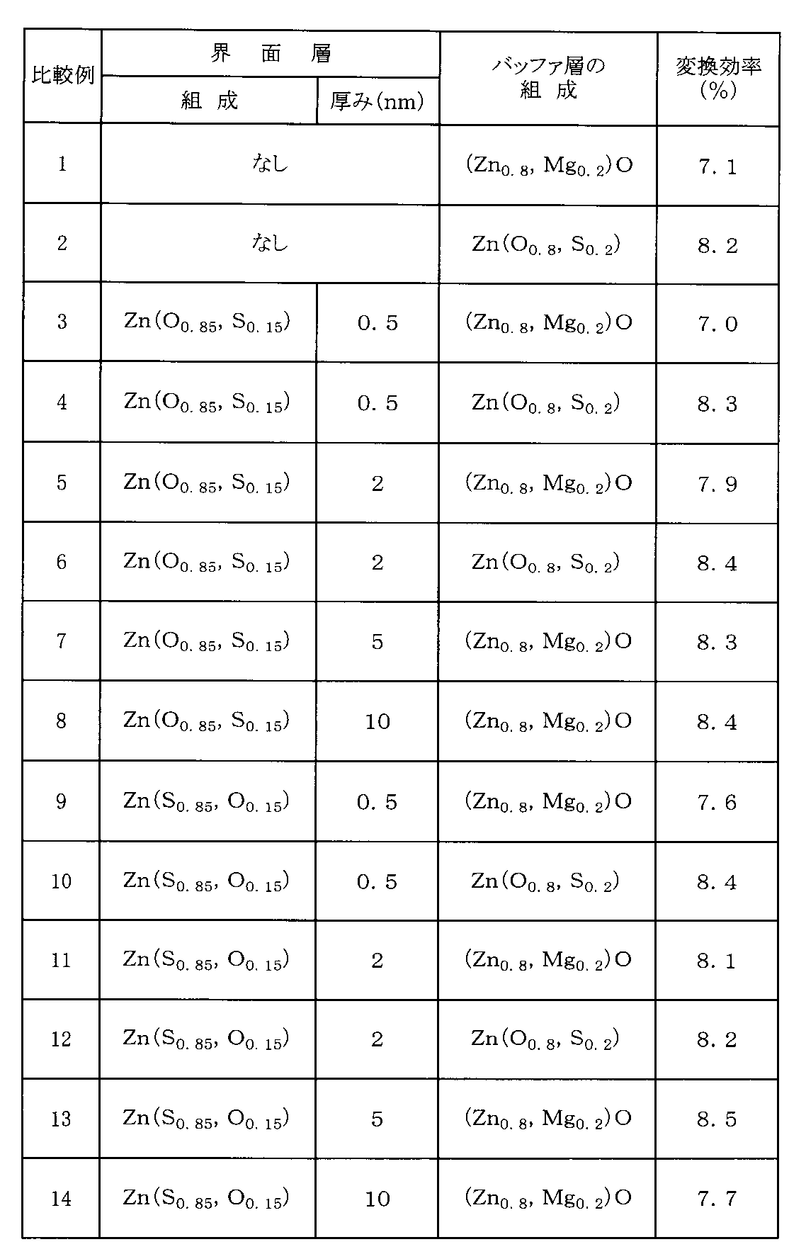
- the conversion efficiency of the CIGS solar cells of Comparative Examples 1 and 2 in which no interface layer was provided was low. This is considered to be caused by reabsorption of carriers at the interface between the CIGS light absorption layer and the buffer layer.
- the CIGS solar cells of Comparative Examples 3 to 14 whose compositions do not satisfy the general formula (1) all have a conversion efficiency of 8.5% or less, and the interface layer is provided. The same low conversion efficiency as in Comparative Examples 1 and 2 was observed.
- the compound solar cell of the present invention is a thin film and has high conversion efficiency, it can be applied to various applications. Further, the method for producing a compound solar cell of the present invention can produce a solar cell efficiently at low cost because the buffer layer can be formed continuously following the previous and subsequent steps without taking it out into the atmosphere. Suitable for
Landscapes
- Photovoltaic Devices (AREA)
- Engineering & Computer Science (AREA)
- Life Sciences & Earth Sciences (AREA)
- Sustainable Energy (AREA)
- Manufacturing & Machinery (AREA)
Abstract
Description


ロールトゥロール方式により、長尺状の基板1を走行させながら、その表面に、Mo等の形成材料を用いて、例えば、スパッタリング法、蒸着法、インクジェット法等により、裏面電極層2を形成する。
つぎに、上記裏面電極層2が形成された基板1を、同じくロールトゥロール方式で走行させながら、その裏面電極層2の上に、CIGS光吸収層3を形成する。CIGS光吸収層3の形成方法としては、例えば、真空蒸着法、セレン化/硫化法、スパッタリング法等があげられる。
そして、上記CIGS光吸収層3までが形成された基板1を、同じくロールトゥロール方式で走行させながら、そのCIGS光吸収層3の上に、界面層4を形成する。界面層4の形成方法としては、例えば、スパッタリング法、蒸着法等があげられる。とりわけ、所望どおりの組成に制御しやすい点から、スパッタリング法が好ましく用いられる。上記スパッタリング法としては、所望どおりの組成の陰極ターゲットを用いるターゲットスパッタリング法でもよいし、Zn材料のスパッタ中に酸素および硫化水素等のカルコゲン分子または化合物を供給する反応性スパッタリング法であってもよく、他の方法であってもよい。また、スパッタリング法に用いる装置は、通常のマグネトロン型スパッタリング装置のほか、2枚の陰極ターゲットを対向して配置する対向ターゲット型スパッタリング装置を用いることができる。対向ターゲット型スパッタリング装置を用いると、対向する陰極ターゲット間にプラズマを閉じ込めることができ、基板1がプラズマに晒されないことから、荷電粒子(電子、イオン)や反跳アルゴンによるダメージが小さく、成膜面やその下地となる面に欠陥やボイドが生じにくいため、好適である。そして、上記一対のターゲットに対する印加は、高周波(RF)電源によるか、高周波(RF)電源に直流(DC)電源を重畳することが好適である。
つぎに、上記界面層4までが形成された基板1を、ロールトゥロール方式で走行させながら、その界面層4の上に、バッファ層5を形成する。バッファ層5の形成方法としては、例えば、溶液成長法、真空蒸着法、CVD法、ALD法、スパッタリング法等があげられる。とりわけ、所望どおりの組成に制御しやすい点から、スパッタリング法が好ましく用いられ、上記界面層4の形成と同様、図2に示すように、陰極ターゲット7,7’が特殊な配置に設定された対向ターゲットスパッタリング装置を用いることが好適である。すなわち、この装置によれば、より少ない電力で成膜することができ、成膜面やその下地となる面が、さらにダメージを受けにくくなるためである。
そして、上記バッファ層5までが形成された基板1を、ロールトゥロール方式で走行させながら、そのバッファ層5の上に、表面電極層6を形成する。表面電極層6の形成方法としては、例えば、スパッタリング法、蒸着法、有機金属気相成長法(MOCVD法)等があげられる。とりわけ、所望どおりの組成に制御しやすい点から、スパッタリング法が好ましく用いられ、上記界面層4およびバッファ層5の形成と同様、図2に示すように、陰極ターゲット7,7’が特殊な配置に設定された対向ターゲットスパッタリング装置を用いることが好適であり、その理由も同様である。
(裏面電極層の形成)
まず、脱脂したソーダライムガラス(厚み0.55mm、幅20mm、長さ20mmの平面視正方形状)からなる基板の表面に、マグネトロンスパッタリング装置(アルバック社製、SH-450)を用いて、放電ガスにはアルゴンを使用し、スパッタリング圧力が1Paとなるよう直流(DC)電源を用い、スパッタリングレート60nm/minの条件で、厚み0.8μmのMoからなる裏面電極層を形成した。
つぎに、上記で形成された裏面電極層の上に、CIGS光吸収層を形成した。すなわち、真空蒸着装置のチャンバー内に、Ga,In,Cu,Seのそれぞれを蒸着源として配置し、このチャンバー内を真空度1×10⁻⁴Paとし、基板温度を250℃にした状態でIn、Ga、Seを同時に32分間蒸着した。その後、基板温度を20℃/分の昇温速度で550℃まで昇温しながらCuおよびSeを同時に33分間蒸着し、最後に基板温度を550℃に保ったままIn、GaおよびSeを同時に蒸着して上記裏面電極層の上にCIGS光吸収層を形成した。上記蒸着源の温度はそれぞれGa:950℃、In:780℃、Cu:1100℃、Se:140℃、となるよう加熱した。得られたCIGS光吸収層の組成(原子数%)は、Cu/III族=0.89、Ga/III族=0.31であり、その厚みは2.1μmであった。
つぎに、図2に示す一対の陰極ターゲットが略V字状に配置された対向ターゲットスパッタ装置(仮想中心軸αに対する角θがそれぞれ10°)を用いて、上記で形成されたCIGS光吸収層の上に、界面層を形成した。なお、陰極ターゲットとして、ZnOからなる組成のものを使用し、スパッタリングの際の放電ガスにArを用い、高周波(RF)電源により、電力100W、スパッタリング圧力0.3Paの条件下で、形成時間を調整することにより、膜厚0.5nmの界面層を得た。
つぎに、上記界面層の形成と同様、図2に示す一対の陰極ターゲットが略V字状に配置された対向ターゲットスパッタ装置(仮想中心軸αに対する角θがそれぞれ10°)を用いて、上記で形成された界面層の上に、バッファ層を形成した。なお、陰極ターゲットとして、Zn0.85Mg0.15Oからなる組成のものを使用し、スパッタリングの際の放電ガスにArを用い、高周波(RF)電源により、電力密度0.7kW/cm2、スパッタリング圧力0.3Paの条件下で、電力および形成時間を調整することにより、膜厚70nmのバッファ層を得た。
つぎに、マグネトロンスパッタリング装置(アルバック社製、SH-450)を用いて、上記で形成されたバッファ層の上に、表面電極層を形成した。なお、陰極ターゲットとして、ITO(In2O3:90〔原子数%〕、SnO2:10〔原子数%〕)を用い、放電ガスにはArとO2(Ar流量の1/10)との混合ガスを使用し、スパッタリング圧力が0.3Paとなるよう高周波(RF)電源を用い、スパッタリングレート20nm/minの条件で、厚み200nmのITOからなる表面電極層を形成した。
製造条件を、後記の表1~3に示すように変更した以外は、実施例1と同様にして、CIGS太陽電池を得た。
界面層を形成せず、製造条件を後記の表4に示すように変更した以外は、実施例1と同様にして、CIGS太陽電池を得た。
製造条件を、後記の表4に示すように変更した以外は、実施例1と同様にして、CIGS太陽電池を得た。
実施例および比較例のCIGS太陽電池をそれぞれ20個準備し、これらに擬似太陽光(Air Mass=1.5)を照射し、IV計測システム(山下電装社製)を用いて、それぞれの変換効率を測定した。

3 CIGS光吸収層
4 界面層
5 バッファ層
6 表面電極層
Claims (4)
- 基板上に、I-III-VI族化合物半導体からなる化合物光吸収層と、バッファ層と、表面電極層とを備えた化合物太陽電池であって、上記化合物光吸収層とバッファ層との間に、下記の一般式(1)に示す組成の混晶からなる界面層を設けることを特徴とする化合物太陽電池。

- 上記バッファ層が、下記の一般式(2)に示す組成の混晶である請求項1記載の化合物太陽電池。
- 上記バッファ層が、下記の一般式(3)に示す組成の混晶である請求項1記載の化合物太陽電池。
- 請求項1記載の化合物太陽電池を製造する方法であって、長尺状の基板を長手方向に走行させながら、上記基板の上にI-III-VI族化合物半導体からなる化合物光吸収層を形成する工程と、界面層を形成する工程と、バッファ層を形成する工程と、表面電極層を形成する工程とを備え、各工程を真空下においてこの順で連続的に行うことを特徴とする化合物太陽電池の製造方法。
Priority Applications (4)
| Application Number | Priority Date | Filing Date | Title |
|---|---|---|---|
| US14/421,580 US10304978B2 (en) | 2012-08-24 | 2013-06-18 | Compound solar cell and production method therefor |
| KR1020157004311A KR20150048728A (ko) | 2012-08-24 | 2013-06-18 | 화합물 태양 전지 및 그 제조 방법 |
| CN201380043997.2A CN104603957B (zh) | 2012-08-24 | 2013-06-18 | 化合物太阳能电池及其制造方法 |
| EP13830458.9A EP2889919B1 (en) | 2012-08-24 | 2013-06-18 | Compound solar cell and method for manufacturing same |
Applications Claiming Priority (2)
| Application Number | Priority Date | Filing Date | Title |
|---|---|---|---|
| JP2012-185197 | 2012-08-24 | ||
| JP2012185197A JP6083785B2 (ja) | 2012-08-24 | 2012-08-24 | 化合物太陽電池およびその製造方法 |
Publications (1)
| Publication Number | Publication Date |
|---|---|
| WO2014030412A1 true WO2014030412A1 (ja) | 2014-02-27 |
Family
ID=50149730
Family Applications (1)
| Application Number | Title | Priority Date | Filing Date |
|---|---|---|---|
| PCT/JP2013/066638 Ceased WO2014030412A1 (ja) | 2012-08-24 | 2013-06-18 | 化合物太陽電池およびその製造方法 |
Country Status (7)
| Country | Link |
|---|---|
| US (1) | US10304978B2 (ja) |
| EP (1) | EP2889919B1 (ja) |
| JP (1) | JP6083785B2 (ja) |
| KR (1) | KR20150048728A (ja) |
| CN (1) | CN104603957B (ja) |
| TW (1) | TWI589011B (ja) |
| WO (1) | WO2014030412A1 (ja) |
Cited By (1)
| Publication number | Priority date | Publication date | Assignee | Title |
|---|---|---|---|---|
| JP2015233139A (ja) * | 2014-06-10 | 2015-12-24 | エスケー イノベーション カンパニー リミテッドSk Innovation Co.,Ltd. | 原子層蒸着法で形成されたバッファ層を含む太陽電池、及び、その製造方法 |
Families Citing this family (6)
| Publication number | Priority date | Publication date | Assignee | Title |
|---|---|---|---|---|
| US9082903B2 (en) | 2010-09-22 | 2015-07-14 | First Solar, Inc. | Photovoltaic device with a zinc magnesium oxide window layer |
| JP6224532B2 (ja) * | 2014-06-27 | 2017-11-01 | 京セラ株式会社 | 光電変換装置 |
| JP7058460B2 (ja) * | 2016-06-30 | 2022-04-22 | ソーラーフロンティア株式会社 | 光電変換モジュール |
| CN111463300A (zh) * | 2019-01-18 | 2020-07-28 | 北京铂阳顶荣光伏科技有限公司 | 薄膜太阳能电池的制备方法及薄膜太阳能电池 |
| CN111463307A (zh) * | 2019-01-18 | 2020-07-28 | 北京铂阳顶荣光伏科技有限公司 | 薄膜太阳能电池及其制备方法 |
| KR102669817B1 (ko) * | 2021-11-16 | 2024-05-28 | 경희대학교 산학협력단 | 야누스 전이금속 디칼코게나이드 박막 및, 야누스 전이금속 디칼코게나이드 박막의 제조 방법 |
Citations (6)
| Publication number | Priority date | Publication date | Assignee | Title |
|---|---|---|---|---|
| JP2000323733A (ja) * | 1999-03-05 | 2000-11-24 | Matsushita Electric Ind Co Ltd | 太陽電池 |
| JP2002124688A (ja) | 2000-10-18 | 2002-04-26 | Matsushita Electric Ind Co Ltd | 太陽電池 |
| JP2002343987A (ja) | 2001-05-15 | 2002-11-29 | Showa Shell Sekiyu Kk | ヘテロ接合薄膜太陽電池の製造方法 |
| JP2004047916A (ja) * | 2002-07-12 | 2004-02-12 | Honda Motor Co Ltd | 化合物薄膜太陽電池およびその製造方法 |
| JP2006525671A (ja) * | 2003-05-08 | 2006-11-09 | ソリブロ エイビー | 薄膜太陽電池 |
| JP2010251525A (ja) * | 2009-04-15 | 2010-11-04 | Fujifilm Corp | 集積型薄膜太陽電池の製造方法及び製造装置 |
Family Cites Families (10)
| Publication number | Priority date | Publication date | Assignee | Title |
|---|---|---|---|---|
| DE4442824C1 (de) * | 1994-12-01 | 1996-01-25 | Siemens Ag | Solarzelle mit Chalkopyrit-Absorberschicht |
| US6259016B1 (en) | 1999-03-05 | 2001-07-10 | Matsushita Electric Industrial Co., Ltd. | Solar cell |
| JP2005228975A (ja) * | 2004-02-13 | 2005-08-25 | Matsushita Electric Ind Co Ltd | 太陽電池 |
| JP4841173B2 (ja) | 2005-05-27 | 2011-12-21 | 昭和シェル石油株式会社 | Cis系薄膜太陽電池の高抵抗バッファ層・窓層連続製膜方法及び製膜装置 |
| US20100051105A1 (en) * | 2008-08-26 | 2010-03-04 | Mustafa Pinarbasi | Flexible substrate for ii-vi compound solar cells |
| JP4745450B2 (ja) * | 2009-10-06 | 2011-08-10 | 富士フイルム株式会社 | バッファ層とその製造方法、反応液、光電変換素子及び太陽電池 |
| CN101764181A (zh) * | 2009-12-03 | 2010-06-30 | 郭玉钦 | 磁控溅射和共蒸发法组合工艺制备铜铟镓硒软体太阳能电池的方法 |
| JP2012004287A (ja) * | 2010-06-16 | 2012-01-05 | Showa Shell Sekiyu Kk | Cis系薄膜太陽電池 |
| JP2012235024A (ja) * | 2011-05-06 | 2012-11-29 | Toshiba Corp | 光電変換素子および太陽電池 |
| CN102337516A (zh) * | 2011-09-29 | 2012-02-01 | 中国建材国际工程集团有限公司 | 一种无镉的铜铟镓硒薄膜太阳能电池缓冲层的沉积方法 |
-
2012
- 2012-08-24 JP JP2012185197A patent/JP6083785B2/ja not_active Expired - Fee Related
-
2013
- 2013-06-18 KR KR1020157004311A patent/KR20150048728A/ko not_active Abandoned
- 2013-06-18 TW TW102121520A patent/TWI589011B/zh not_active IP Right Cessation
- 2013-06-18 CN CN201380043997.2A patent/CN104603957B/zh not_active Expired - Fee Related
- 2013-06-18 US US14/421,580 patent/US10304978B2/en not_active Expired - Fee Related
- 2013-06-18 WO PCT/JP2013/066638 patent/WO2014030412A1/ja not_active Ceased
- 2013-06-18 EP EP13830458.9A patent/EP2889919B1/en not_active Not-in-force
Patent Citations (6)
| Publication number | Priority date | Publication date | Assignee | Title |
|---|---|---|---|---|
| JP2000323733A (ja) * | 1999-03-05 | 2000-11-24 | Matsushita Electric Ind Co Ltd | 太陽電池 |
| JP2002124688A (ja) | 2000-10-18 | 2002-04-26 | Matsushita Electric Ind Co Ltd | 太陽電池 |
| JP2002343987A (ja) | 2001-05-15 | 2002-11-29 | Showa Shell Sekiyu Kk | ヘテロ接合薄膜太陽電池の製造方法 |
| JP2004047916A (ja) * | 2002-07-12 | 2004-02-12 | Honda Motor Co Ltd | 化合物薄膜太陽電池およびその製造方法 |
| JP2006525671A (ja) * | 2003-05-08 | 2006-11-09 | ソリブロ エイビー | 薄膜太陽電池 |
| JP2010251525A (ja) * | 2009-04-15 | 2010-11-04 | Fujifilm Corp | 集積型薄膜太陽電池の製造方法及び製造装置 |
Non-Patent Citations (3)
| Title |
|---|
| D. HARISKOS ET AL.: "The Zn(S,O,OH)/ZnMgO buffer in thin-film Cu(In,Ga)(Se,S)2-based solar cells part II: Magnetron sputtering of the ZnMgO buffer layer for in-line co- evaporated Cu(In,Ga)Se2 solar cells", PROGRESS IN PHOTOVOLTAICS: RESEARCH AND APPLICATIONS, vol. 17, 2009, pages 479 - 488, XP055104707 * |
| MINEMOTO, CURRENT APPLIED PHYSICS, vol. 10, no. 2, March 2010 (2010-03-01), pages S150 - S153 |
| See also references of EP2889919A4 |
Cited By (1)
| Publication number | Priority date | Publication date | Assignee | Title |
|---|---|---|---|---|
| JP2015233139A (ja) * | 2014-06-10 | 2015-12-24 | エスケー イノベーション カンパニー リミテッドSk Innovation Co.,Ltd. | 原子層蒸着法で形成されたバッファ層を含む太陽電池、及び、その製造方法 |
Also Published As
| Publication number | Publication date |
|---|---|
| TW201409728A (zh) | 2014-03-01 |
| CN104603957A (zh) | 2015-05-06 |
| JP6083785B2 (ja) | 2017-02-22 |
| TWI589011B (zh) | 2017-06-21 |
| JP2014045000A (ja) | 2014-03-13 |
| EP2889919A4 (en) | 2016-04-20 |
| KR20150048728A (ko) | 2015-05-07 |
| EP2889919B1 (en) | 2019-02-20 |
| US10304978B2 (en) | 2019-05-28 |
| EP2889919A1 (en) | 2015-07-01 |
| CN104603957B (zh) | 2017-09-15 |
| US20150303329A1 (en) | 2015-10-22 |
Similar Documents
| Publication | Publication Date | Title |
|---|---|---|
| JP6083785B2 (ja) | 化合物太陽電池およびその製造方法 | |
| CN102652368B (zh) | 太阳能电池中使用的Cu-In-Zn-Sn-(Se,S)基薄膜及其制造方法 | |
| KR101628312B1 (ko) | CZTSSe계 박막 태양전지의 제조방법 및 이에 의해 제조된 CZTSSe계 박막 태양전지 | |
| US20150303346A1 (en) | Method for manufacturing compound solar cell | |
| CN104137272B (zh) | Cigs系化合物太阳能电池 | |
| KR101777598B1 (ko) | 태양전지 제조방법 | |
| CN104995749B (zh) | Cigs系化合物太阳能电池 | |
| JP2014225567A (ja) | Cigs系化合物太陽電池およびその製造方法 | |
| KR102066053B1 (ko) | 소다석회유리 절연층을 포함하는 플렉시블 박막 태양전지 및 그 제조방법 | |
| JP2014017377A (ja) | 化合物太陽電池およびその製法 | |
| KR20150136721A (ko) | 고품질 cigs 광흡수층을 포함하는 태양전지 및 이의 제조방법 | |
| KR20150136722A (ko) | 고품질 cigs 광흡수층을 포함하는 태양전지 및 이의 제조방법 |
Legal Events
| Date | Code | Title | Description |
|---|---|---|---|
| 121 | Ep: the epo has been informed by wipo that ep was designated in this application |
Ref document number: 13830458 Country of ref document: EP Kind code of ref document: A1 |
|
| WWE | Wipo information: entry into national phase |
Ref document number: 14421580 Country of ref document: US |
|
| WWE | Wipo information: entry into national phase |
Ref document number: 2013830458 Country of ref document: EP |
|
| ENP | Entry into the national phase |
Ref document number: 20157004311 Country of ref document: KR Kind code of ref document: A |
|
| NENP | Non-entry into the national phase |
Ref country code: DE |