WO2014030453A1 - 炭化珪素半導体装置の製造方法 - Google Patents
炭化珪素半導体装置の製造方法 Download PDFInfo
- Publication number
- WO2014030453A1 WO2014030453A1 PCT/JP2013/068849 JP2013068849W WO2014030453A1 WO 2014030453 A1 WO2014030453 A1 WO 2014030453A1 JP 2013068849 W JP2013068849 W JP 2013068849W WO 2014030453 A1 WO2014030453 A1 WO 2014030453A1
- Authority
- WO
- WIPO (PCT)
- Prior art keywords
- silicon carbide
- semiconductor device
- layer
- trench
- main surface
- Prior art date
- Legal status (The legal status is an assumption and is not a legal conclusion. Google has not performed a legal analysis and makes no representation as to the accuracy of the status listed.)
- Ceased
Links
Images







Classifications
-
- H—ELECTRICITY
- H10—SEMICONDUCTOR DEVICES; ELECTRIC SOLID-STATE DEVICES NOT OTHERWISE PROVIDED FOR
- H10D—INORGANIC ELECTRIC SEMICONDUCTOR DEVICES
- H10D30/00—Field-effect transistors [FET]
- H10D30/01—Manufacture or treatment
- H10D30/021—Manufacture or treatment of FETs having insulated gates [IGFET]
- H10D30/025—Manufacture or treatment of FETs having insulated gates [IGFET] of vertical IGFETs
-
- H—ELECTRICITY
- H10—SEMICONDUCTOR DEVICES; ELECTRIC SOLID-STATE DEVICES NOT OTHERWISE PROVIDED FOR
- H10D—INORGANIC ELECTRIC SEMICONDUCTOR DEVICES
- H10D30/00—Field-effect transistors [FET]
- H10D30/60—Insulated-gate field-effect transistors [IGFET]
- H10D30/64—Double-diffused metal-oxide semiconductor [DMOS] FETs
- H10D30/66—Vertical DMOS [VDMOS] FETs
- H10D30/668—Vertical DMOS [VDMOS] FETs having trench gate electrodes, e.g. UMOS transistors
-
- H—ELECTRICITY
- H10—SEMICONDUCTOR DEVICES; ELECTRIC SOLID-STATE DEVICES NOT OTHERWISE PROVIDED FOR
- H10D—INORGANIC ELECTRIC SEMICONDUCTOR DEVICES
- H10D12/00—Bipolar devices controlled by the field effect, e.g. insulated-gate bipolar transistors [IGBT]
- H10D12/01—Manufacture or treatment
- H10D12/031—Manufacture or treatment of IGBTs
-
- H—ELECTRICITY
- H10—SEMICONDUCTOR DEVICES; ELECTRIC SOLID-STATE DEVICES NOT OTHERWISE PROVIDED FOR
- H10D—INORGANIC ELECTRIC SEMICONDUCTOR DEVICES
- H10D30/00—Field-effect transistors [FET]
- H10D30/01—Manufacture or treatment
- H10D30/021—Manufacture or treatment of FETs having insulated gates [IGFET]
- H10D30/028—Manufacture or treatment of FETs having insulated gates [IGFET] of double-diffused metal oxide semiconductor [DMOS] FETs
- H10D30/0291—Manufacture or treatment of FETs having insulated gates [IGFET] of double-diffused metal oxide semiconductor [DMOS] FETs of vertical DMOS [VDMOS] FETs
- H10D30/0297—Manufacture or treatment of FETs having insulated gates [IGFET] of double-diffused metal oxide semiconductor [DMOS] FETs of vertical DMOS [VDMOS] FETs using recessing of the gate electrodes, e.g. to form trench gate electrodes
-
- H—ELECTRICITY
- H10—SEMICONDUCTOR DEVICES; ELECTRIC SOLID-STATE DEVICES NOT OTHERWISE PROVIDED FOR
- H10D—INORGANIC ELECTRIC SEMICONDUCTOR DEVICES
- H10D62/00—Semiconductor bodies, or regions thereof, of devices having potential barriers
- H10D62/80—Semiconductor bodies, or regions thereof, of devices having potential barriers characterised by the materials
- H10D62/83—Semiconductor bodies, or regions thereof, of devices having potential barriers characterised by the materials being Group IV materials, e.g. B-doped Si or undoped Ge
- H10D62/832—Semiconductor bodies, or regions thereof, of devices having potential barriers characterised by the materials being Group IV materials, e.g. B-doped Si or undoped Ge being Group IV materials comprising two or more elements, e.g. SiGe
- H10D62/8325—Silicon carbide
-
- H—ELECTRICITY
- H10—SEMICONDUCTOR DEVICES; ELECTRIC SOLID-STATE DEVICES NOT OTHERWISE PROVIDED FOR
- H10P—GENERIC PROCESSES OR APPARATUS FOR THE MANUFACTURE OR TREATMENT OF DEVICES COVERED BY CLASS H10
- H10P50/00—Etching of wafers, substrates or parts of devices
- H10P50/20—Dry etching; Plasma etching; Reactive-ion etching
- H10P50/24—Dry etching; Plasma etching; Reactive-ion etching of semiconductor materials
- H10P50/242—Dry etching; Plasma etching; Reactive-ion etching of semiconductor materials of Group IV materials
-
- H—ELECTRICITY
- H10—SEMICONDUCTOR DEVICES; ELECTRIC SOLID-STATE DEVICES NOT OTHERWISE PROVIDED FOR
- H10P—GENERIC PROCESSES OR APPARATUS FOR THE MANUFACTURE OR TREATMENT OF DEVICES COVERED BY CLASS H10
- H10P50/00—Etching of wafers, substrates or parts of devices
- H10P50/69—Etching of wafers, substrates or parts of devices using masks for semiconductor materials
- H10P50/691—Etching of wafers, substrates or parts of devices using masks for semiconductor materials for Group V materials or Group III-V materials
- H10P50/693—Etching of wafers, substrates or parts of devices using masks for semiconductor materials for Group V materials or Group III-V materials characterised by their size, orientation, disposition, behaviour or shape, in horizontal or vertical plane
- H10P50/695—Etching of wafers, substrates or parts of devices using masks for semiconductor materials for Group V materials or Group III-V materials characterised by their size, orientation, disposition, behaviour or shape, in horizontal or vertical plane characterised by the process involved to create the mask, e.g. lift-off masks or sidewalls or to modify the mask
-
- H—ELECTRICITY
- H10—SEMICONDUCTOR DEVICES; ELECTRIC SOLID-STATE DEVICES NOT OTHERWISE PROVIDED FOR
- H10P—GENERIC PROCESSES OR APPARATUS FOR THE MANUFACTURE OR TREATMENT OF DEVICES COVERED BY CLASS H10
- H10P70/00—Cleaning of wafers, substrates or parts of devices
- H10P70/20—Cleaning during device manufacture
- H10P70/23—Cleaning during device manufacture during, before or after processing of insulating materials
-
- H—ELECTRICITY
- H10—SEMICONDUCTOR DEVICES; ELECTRIC SOLID-STATE DEVICES NOT OTHERWISE PROVIDED FOR
- H10D—INORGANIC ELECTRIC SEMICONDUCTOR DEVICES
- H10D62/00—Semiconductor bodies, or regions thereof, of devices having potential barriers
- H10D62/40—Crystalline structures
- H10D62/405—Orientations of crystalline planes
-
- H—ELECTRICITY
- H10—SEMICONDUCTOR DEVICES; ELECTRIC SOLID-STATE DEVICES NOT OTHERWISE PROVIDED FOR
- H10D—INORGANIC ELECTRIC SEMICONDUCTOR DEVICES
- H10D64/00—Electrodes of devices having potential barriers
- H10D64/20—Electrodes characterised by their shapes, relative sizes or dispositions
- H10D64/27—Electrodes not carrying the current to be rectified, amplified, oscillated or switched, e.g. gates
- H10D64/311—Gate electrodes for field-effect devices
- H10D64/411—Gate electrodes for field-effect devices for FETs
- H10D64/511—Gate electrodes for field-effect devices for FETs for IGFETs
- H10D64/512—Disposition of the gate electrodes, e.g. buried gates
- H10D64/513—Disposition of the gate electrodes, e.g. buried gates within recesses in the substrate, e.g. trench gates, groove gates or buried gates
-
- H—ELECTRICITY
- H10—SEMICONDUCTOR DEVICES; ELECTRIC SOLID-STATE DEVICES NOT OTHERWISE PROVIDED FOR
- H10D—INORGANIC ELECTRIC SEMICONDUCTOR DEVICES
- H10D64/00—Electrodes of devices having potential barriers
- H10D64/60—Electrodes characterised by their materials
- H10D64/66—Electrodes having a conductor capacitively coupled to a semiconductor by an insulator, e.g. MIS electrodes
- H10D64/68—Electrodes having a conductor capacitively coupled to a semiconductor by an insulator, e.g. MIS electrodes characterised by the insulator, e.g. by the gate insulator
- H10D64/693—Electrodes having a conductor capacitively coupled to a semiconductor by an insulator, e.g. MIS electrodes characterised by the insulator, e.g. by the gate insulator the insulator comprising nitrogen, e.g. nitrides, oxynitrides or nitrogen-doped materials
Definitions
- the present invention relates to a method for manufacturing a silicon carbide semiconductor device, and particularly to a method for manufacturing a silicon carbide semiconductor device having a silicon carbide substrate in which a trench is formed.
- Patent Document 1 a method for manufacturing a MOSFET (Metal Oxide Semiconductor Field Effect Transistor) having a silicon carbide substrate with a trench formed therein is disclosed.
- the trench is formed as follows. First, a silicon oxide film is formed on a silicon carbide substrate by a CVD (Chemical Vapor Deposition) method. A resist film having a predetermined opening pattern is formed on the silicon oxide film by using a photolithography method. By etching the silicon oxide film using this resist film as a mask, a mask layer having an opening pattern is formed on the silicon carbide substrate. A preliminary trench is formed in the silicon carbide substrate by RIE using this mask layer as a mask. Next, thermal etching is performed to form a final trench in the silicon carbide substrate.
- CVD Chemical Vapor Deposition
- an etching residue may exist on the silicon carbide substrate in the opening pattern.
- thermal etching is performed in a state where a residue exists on the silicon carbide substrate, a protrusion corresponding to the residue can be formed in the trench. That is, the surface of the trench may be roughened.
- the breakdown voltage of the silicon carbide semiconductor device may be reduced.
- RIE is performed prior to thermal etching, the residue can be removed to some extent, but due to a residue newly generated by a reaction product of RIE, the residue can be sufficiently removed. Have difficulty.
- the surface roughness caused by RIE may cause surface roughness after the subsequent thermal etching, and may cause a decrease in breakdown voltage as described above.
- the present invention has been made to solve such a problem, and an object of the present invention is to provide a method for manufacturing a silicon carbide semiconductor device capable of suppressing a decrease in breakdown voltage due to surface roughness in a trench. Is to provide.
- the method for manufacturing a silicon carbide semiconductor device of the present invention includes the following steps.
- a silicon carbide substrate having a main surface covered with a silicon dioxide layer is prepared.
- a photoresist layer having a pattern is formed on the silicon dioxide layer.
- an opening exposing a part of the main surface is formed in the silicon dioxide layer.
- Etching residue is present on a portion of the main surface exposed by the opening.
- Residues are removed by plasma etching in which only an inert gas is introduced.
- a reactive gas is supplied under heating to the silicon carbide substrate having the main surface covered with the silicon dioxide layer in which the opening is formed.
- a trench having a sidewall surface is formed.
- a gate insulating film is formed on the side wall surface of the trench.
- a gate electrode is formed on the gate insulating film.
- the gas introduced in the plasma etching for removing the residue is only the inert gas.
- the plasma etching is performed in an atmosphere having a residual oxygen amount of 1% or less.
- production of the new residue by an oxidation reaction can be suppressed.
- the reactive gas contains a halogen gas.
- thermal etching can be performed using a reaction between a halogen gas and silicon carbide.
- the reactive gas contains oxygen gas.
- oxygen gas oxygen gas
- the number density of protrusions having a height of 10 nm or more is 1 cm ⁇ 2 or less on the main surface where the trench is formed.
- the fall of the proof pressure resulting from the surface roughness in a trench can fully be suppressed.
- FIG. 1 is a partial cross sectional view schematically showing a configuration of a silicon carbide semiconductor device in one embodiment of the present invention.
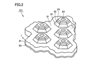
- FIG. 2 is a partial perspective view schematically showing a shape of a silicon carbide substrate included in the silicon carbide semiconductor device of FIG. 1.
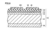
- FIG. 8 is a partial cross sectional view schematically showing a first step of the method for manufacturing the silicon carbide semiconductor device of FIG. 1.
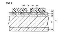
- FIG. 8 is a partial cross sectional view schematically showing a second step of the method for manufacturing the silicon carbide semiconductor device of FIG. 1.
- FIG. 8 is a partial cross sectional view schematically showing a third step of the method for manufacturing the silicon carbide semiconductor device of FIG. 1.
- FIG. 8 is a partial cross sectional view schematically showing a fourth step of the method for manufacturing the silicon carbide semiconductor device of FIG. 1.
- FIG. 8 is a partial cross sectional view schematically showing a fifth step of the method for manufacturing the silicon carbide semiconductor device of FIG. 1.
- FIG. 8 is a partial cross sectional view schematically showing a sixth step of the method for manufacturing the silicon carbide semiconductor device of FIG. 1.
- FIG. 8 is a partial cross sectional view schematically showing a seventh step of the method for manufacturing the silicon carbide semiconductor device of FIG. 1.
- FIG. 12 is a partial cross sectional view schematically showing an eighth step of the method for manufacturing the silicon carbide semiconductor device of FIG. 1.
- FIG. 11 is a partially enlarged view of FIG. 10 and shows the presence of a residue.
- FIG. 11 is a partially enlarged view of FIG. 10 and shows the presence of a residue.
- FIG. 12 is a partial cross sectional view schematically showing a ninth step of the method for manufacturing the silicon carbide semiconductor device of FIG. 1.
- FIG. 12 is a partial cross sectional view schematically showing a tenth step of the method for manufacturing the silicon carbide semiconductor device of FIG. 1.
- FIG. 12 is a partial cross sectional view schematically showing an eleventh step of the method for manufacturing the silicon carbide semiconductor device of FIG. 1.
- FIG. 12 is a partial cross sectional view schematically showing a twelfth step of the method for manufacturing the silicon carbide semiconductor device of FIG. 1.
- FIG. 14 is a partial cross sectional view schematically showing a thirteenth step of the method for manufacturing the silicon carbide semiconductor device of FIG. 1.
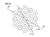
- FIG. 3 is a diagram showing a crystal structure of a (000-1) plane in polytype 4H hexagonal crystal.
- FIG. 20 is a view showing a crystal structure of a (11-20) plane along line XIX-XIX in FIG.
- FIG. 20 is a view showing a crystal structure in the vicinity of the surface of the composite surface in FIG. 17 in the (11-20) plane.
- FIG. 18 is a view of the composite surface of FIG. 17 viewed from the (01-10) plane.
- FIG. 5 is a graph showing an example of a relationship between a channel surface and a (000-1) plane viewed macroscopically and channel mobility when a thermal etching is performed and when it is not performed. It is. It is a graph which shows an example of the relationship between the angle between a channel direction and the ⁇ 0-11-2> direction, and channel mobility. It is a figure which shows the modification of FIG.
- MOSFET 201 silicon carbide semiconductor device of the present embodiment includes an epitaxial substrate 101 (silicon carbide substrate), a gate oxide film 91 (gate insulating film), a gate electrode 92, Interlayer insulating film 93, source electrode 94, source wiring layer 95, and drain electrode 98 are provided.
- Epitaxial substrate 101 is made of silicon carbide, and preferably has polytype 4H.
- the epitaxial substrate 101 includes a single crystal substrate 80 and an epitaxial layer that is provided thereon and forms the main surface MS. This epitaxial layer has an n drift layer 81, a p base layer 82, an n region 83, and a p contact region 84.
- Single crystal substrate 80 has n-type (first conductivity type).
- N drift layer 81 is an epitaxial layer formed on single crystal substrate 80.
- N drift layer 81 has n type.
- the impurity concentration of n drift layer 81 is preferably lower than the impurity concentration of single crystal substrate 80.
- the donor concentration of n drift layer 81 is preferably not less than 1 ⁇ 10 15 cm ⁇ 3 and not more than 5 ⁇ 10 16 cm ⁇ 3 , for example, 8 ⁇ 10 15 cm ⁇ 3 .
- the p base layer 82 has p type.
- the p base layer 82 is provided on the n drift layer 81.
- the impurity concentration of the p base layer 82 is, for example, 1 ⁇ 10 18 cm ⁇ 3 .
- N region 83 has n type.
- N region 83 is provided on p base layer 82 so as to be separated from n drift layer 81 by p base layer 82.
- the p contact region 84 has p type. The p contact region 84 is connected to the p base layer 82.
- a trench TR is provided on the surface of the epitaxial substrate 101 opposite to the single crystal substrate 80 (upper surface in FIG. 1), that is, the main surface MS.
- Trench TR has side wall surface SW and bottom surface BT.
- Sidewall surface SW passes through n region 83 and p base layer 82 and reaches n drift layer 81.
- Sidewall surface SW includes the channel surface of MOSFET 201 on p base layer 82.
- the side wall surface SW is inclined with respect to the main surface MS (upper surface in FIG. 1) of the epitaxial substrate 101, whereby the trench TR expands in a tapered shape toward the opening.
- the plane orientation of the side wall surface SW is preferably inclined at 50 ° or more and 65 ° or less with respect to the (000-1) plane.
- side wall surface SW has a predetermined crystal plane (also referred to as a special plane), particularly in a portion on p base layer 82. Details of the special surface will be described later.
- Bottom surface BT is located on n drift layer 81. In the present embodiment, it has a flat shape substantially parallel to main surface MS of epitaxial substrate 101.
- the gate oxide film 91 covers each of the side wall surface SW and the bottom surface BT of the trench TR.
- the gate electrode 92 is provided on the gate oxide film 91.
- Source electrode 94 is in contact with each of n region 83 and p contact region 84.
- the source wiring layer 95 is in contact with the source electrode 94.
- Source wiring layer 95 is, for example, an aluminum layer.
- the interlayer insulating film 93 insulates between the gate electrode 92 and the source wiring layer 95.
- n drift layer 81 is formed by epitaxial growth of silicon carbide on single crystal substrate 80.
- the plane of the single crystal substrate 80 on which epitaxial growth is performed preferably has an off angle within 8 degrees from the ⁇ 000-1 ⁇ plane, and more preferably has an off angle within 8 degrees from the (000-1) plane. preferable.
- Epitaxial growth can be performed by a CVD (Chemical Vapor Deposition) method.
- the source gas for example, a mixed gas of silane (SiH 4 ) and propane (C 3 H 8 ) can be used. At this time, it is preferable to introduce, for example, nitrogen (N) or phosphorus (P) as impurities.
- an epitaxial substrate 101 is obtained by forming a p base layer 82 and an n region 83 on an n drift layer 81. These can be formed by ion implantation on the entire surface of the n drift layer 81, for example.
- an impurity for imparting p-type such as aluminum (Al)
- Al aluminum
- n region 83 an impurity for imparting n-type, such as phosphorus (P)
- epitaxial growth may be used with the addition of impurities.
- a resist layer 60 is formed on the n region 83 of the epitaxial substrate 101.
- the resist layer 60 is exposed and developed.
- a resist layer 61 (FIG. 6) having an opening corresponding to the position where the p contact region 84 is to be formed is formed.
- the p contact region 84 is formed by ion implantation using the resist layer 61.
- the resist layer 61 is removed (FIG. 7).
- a heat treatment for activating the impurities is performed.
- the temperature of this heat treatment is preferably 1500 ° C. or higher and 1900 ° C. or lower, for example, about 1700 ° C.
- the heat treatment time is, for example, about 30 minutes.
- the atmosphere of the heat treatment is preferably an inert gas atmosphere, for example, an argon (Ar) atmosphere.
- mask layer 40 (silicon dioxide layer) is formed on main surface MS including n region 83 and p contact region 84.
- the epitaxial substrate 101 having the main surface MS covered with the mask layer 40 is prepared.
- mask layer 40 is formed by thermal oxidation of main surface MS.
- a photoresist layer 30 having a pattern is formed on the mask layer 40 by applying, drying, exposing and developing a photoresist. The opening of the pattern is formed corresponding to the position of trench TR (FIG. 1).
- an opening OP exposing a part of the main surface MS is formed in the mask layer 40 by etching using the photoresist layer 30 as a mask.
- the photoresist layer 30 is removed (FIG. 10).
- the residue RS generated during the etching for forming the opening OP exists on a part of the main surface MS exposed by the opening OP.
- This residue RS is removed by plasma etching in which only an inert gas is introduced.
- the plasma etching is performed in an atmosphere having a residual oxygen amount of about 1% or less.
- the pressure of plasma etching is about 0.1 Pa after the etching chamber (not shown) is evacuated to about 1 ⁇ 10 ⁇ 4 Pa or less before plasma etching, the residual oxygen amount in the etching chamber during plasma etching is reduced. It can be about 1% or less.
- a reactive gas is supplied under heating to the epitaxial substrate 101 having the main surface MS covered with the mask layer 40 in which the opening OP is formed.
- trench TR is formed in main surface MS of epitaxial substrate 101.
- the reactive gas for thermal etching preferably contains a halogen gas.
- the halogen gas for example, chlorine gas can be used.
- the reactive gas preferably contains oxygen gas.
- a mixed gas of chlorine gas and oxygen gas is used as the reactive gas.
- the temperature of epitaxial substrate 101 in the thermal etching is, for example, about 700 ° C. or higher and about 1000 ° C. or lower.
- the reaction gas may contain a carrier gas in addition to the above-described chlorine gas and oxygen gas.
- a carrier gas for example, nitrogen gas, argon gas or helium gas can be used.
- the heat treatment temperature is set to 700 ° C. or higher and 1000 ° C. or lower as described above, the etching rate of silicon carbide is about 70 ⁇ m / hour, for example.
- the mask layer 40 made of silicon dioxide has a very high selectivity with respect to silicon carbide, so that it is not substantially etched during the etching of silicon carbide.
- the mask layer 40 is removed by an arbitrary method such as etching.
- the protrusion PR As shown in FIG. 13, due to the influence of the residue RS (FIG. 11) that existed before the thermal etching, the protrusion PR having a height HT of 10 nm or more is formed on the main surface MS where the trench TR is formed by the thermal etching. Can be formed.
- the residue RS is at least partially removed as described above before the thermal etching, the generation of the protrusion PR is suppressed.
- a value obtained by dividing the number of protrusions PR on the entire main surface MS of the epitaxial substrate 101 (FIG. 12) by the total area of the main surface MS of the epitaxial substrate 101 (FIG. 12), that is, the number density of the protrusions PR is 1 cm ⁇ 2 or less.
- gate oxide film 91 is formed on sidewall surface SW and bottom surface BT of trench TR.
- Gate oxide film 91 can be formed, for example, by thermal oxidation.
- the temperature profile has, for example, conditions of a temperature of 1100 ° C. to 1300 ° C. and a holding time of about 1 hour.
- nitrogen atoms are introduced into the interface region between gate oxide film 91 and p base layer 82.
- a gas other than NO gas may be used as the atmospheric gas.
- Ar annealing using argon (Ar) as an atmospheric gas may be further performed.
- the heating temperature for Ar annealing is preferably higher than the heating temperature for NO annealing and lower than the melting point of the gate oxide film 91.
- the time during which this heating temperature is maintained is, for example, about 1 hour. Thereby, the formation of interface states in the interface region between gate oxide film 91 and p base layer 82 is further suppressed.
- other inert gas such as nitrogen gas may be used as the atmospheric gas instead of Ar gas.
- a gate electrode 92 is formed on the gate oxide film 91.
- gate electrode 92 is formed on gate oxide film 91 so as to fill the region inside trench TR with gate oxide film 91 interposed therebetween.
- the gate electrode 92 can be formed by, for example, forming a conductor or doped polysilicon and CMP.
- interlayer insulating film 93 is formed on gate electrode 92 and gate oxide film 91 so as to cover the exposed surface of gate electrode 92. Etching is performed so that openings are formed in the interlayer insulating film 93 and the gate oxide film 91. Through this opening, each of n region 83 and p contact region 84 is exposed on main surface MS. Next, source electrode 94 in contact with each of n region 83 and n contact region 84 is formed on main surface MS. A drain electrode 98 is formed on n drift layer 81 through single crystal substrate 80.
- source wiring layer 95 is formed. Thereby, MOSFET 201 is obtained.
- the gas introduced in the plasma etching for removing the residue RS is only an inert gas.
- the gas introduced in the plasma etching for removing the residue RS is only an inert gas.
- thermal etching can be performed with a small amount of residue RS. Therefore, the formation of the protrusion PR (FIG. 13) in the thermal etching is suppressed. Therefore, it is possible to suppress a decrease in breakdown voltage due to surface roughness in the trench TR.
- the plasma etching is performed in an atmosphere having a residual oxygen amount of 1% or less.
- the reactive gas includes a halogen gas.
- thermal etching can be performed using a reaction between a halogen gas and silicon carbide.
- the reactive gas includes oxygen gas.
- carbon generated during the thermal etching is efficiently removed, so that the speed of the thermal etching can be increased.
- the number density of projections PR (FIG. 13) having a height of 10 nm or more is 1 cm ⁇ 2 or less on main surface MS where trench TR is formed. As a result, it is possible to sufficiently suppress a decrease in breakdown voltage due to surface roughness in the trench TR.
- the side wall surface SW preferably has a special surface, and this case will be described below.
- the side wall surface SW having a special surface includes a surface S1 (first surface).
- the plane S1 has a plane orientation ⁇ 0-33-8 ⁇ , and preferably has a plane orientation (0-33-8).
- the side wall surface SW includes the surface S1 microscopically.
- side wall surface SW further includes a surface S2 (second surface) microscopically.
- the plane S2 has a plane orientation ⁇ 0-11-1 ⁇ , and preferably has a plane orientation (0-11-1).
- “microscopic” means that the dimensions are as detailed as at least a dimension of about twice the atomic spacing.
- TEM Transmission Electron Microscope
- side wall surface SW has composite surface SR.
- the composite surface SR is configured by periodically repeating the surfaces S1 and S2. Such a periodic structure can be observed by, for example, TEM or AFM (Atomic Force Microscopy).
- Composite surface SR has a plane orientation ⁇ 0-11-2 ⁇ , preferably a plane orientation (0-11-2). In this case, the composite surface SR has an off angle of 62 ° macroscopically with respect to the ⁇ 000-1 ⁇ plane.
- “macroscopic” means ignoring a fine structure having a dimension on the order of atomic spacing. As such a macroscopic off-angle measurement, for example, a general method using X-ray diffraction can be used.
- the channel direction CD which is the direction in which carriers flow on the channel surface, is along the direction in which the above-described periodic repetition is performed.
- Si atoms are atoms of A layer (solid line in the figure), B layer atoms (broken line in the figure) located below, C layer atoms (dotted line in the figure) located below, and B layer atoms (not shown) located below this It is provided repeatedly. That is, a periodic laminated structure such as ABCBABCBABCB... Is provided with four layers ABCB as one period.
- the atoms in each of the four layers ABCB constituting one cycle described above are (0-11-2) It is not arranged to be completely along the plane.
- the (0-11-2) plane is shown so as to pass through the position of atoms in the B layer.
- the atoms in the A layer and the C layer are separated from the (0-11-2) plane.
- a surface S1 having a surface orientation (0-33-8) and a surface S2 connected to the surface S1 and having a surface orientation different from the surface orientation of the surface S1 are alternately provided. It is configured by being.
- the length of each of the surface S1 and the surface S2 is twice the atomic spacing of Si atoms (or C atoms).
- the surface obtained by averaging the surfaces S1 and S2 corresponds to the (0-11-2) surface (FIG. 19).
- the single crystal structure periodically includes a structure (surface S1 portion) equivalent to a cubic crystal when viewed partially.
- a surface S1 having a surface orientation (001) in a structure equivalent to the above-described cubic crystal and a surface S2 connected to the surface S1 and having a surface orientation different from the surface orientation of the surface S1 are alternated. It is comprised by being provided in.
- polytypes other than 4H may constitute the surface according to S2).
- the polytype may be 6H or 15R, for example.
- the horizontal axis represents the angle D1 formed by the macroscopic plane orientation of the side wall surface SW having the channel surface and the (000-1) plane
- the vertical axis represents the mobility MB.
- the plot group CM corresponds to the case where the side wall surface SW is finished as a special surface by thermal etching
- the plot group MC corresponds to the case where such thermal etching is not performed.
- the mobility MB in the plot group MC was maximized when the macroscopic surface orientation of the channel surface was (0-33-8). This is because, when thermal etching is not performed, that is, when the microscopic structure of the channel surface is not particularly controlled, the macroscopic plane orientation is set to (0-33-8). This is probably because the ratio of the formation of the visual plane orientation (0-33-8), that is, the plane orientation (0-33-8) considering the atomic level, stochastically increased.
- the mobility MB in the plot group CM was maximized when the macroscopic surface orientation of the channel surface was (0-11-2) (arrow EX).
- the reason for this is that, as shown in FIGS. 20 and 21, a large number of surfaces S1 having a plane orientation (0-33-8) are regularly and densely arranged via the surface S2, so that the surface of the channel surface is fine. This is probably because the proportion of the visual plane orientation (0-33-8) has increased.
- the mobility MB has an orientation dependency on the composite surface SR.
- the horizontal axis indicates the angle D2 between the channel direction and the ⁇ 0-11-2> direction
- the vertical axis indicates the mobility MB (arbitrary unit) of the channel surface.
- a broken line is added to make the graph easier to see.
- the angle D2 of the channel direction CD (FIG. 17) is preferably 0 ° or more and 60 ° or less, and more preferably approximately 0 °. all right.
- the side wall surface SW may further include a surface S3 (third surface) in addition to the composite surface SR (shown in a simplified manner as a straight line in FIG. 24).
- the off angle of the side wall surface SW with respect to the ⁇ 000-1 ⁇ plane deviates from 62 ° which is the ideal off angle of the composite surface SR. This deviation is preferably small and preferably within a range of ⁇ 10 °.
- a surface included in such an angle range for example, there is a surface whose macroscopic plane orientation is a ⁇ 0-33-8 ⁇ plane.
- the off angle of the side wall surface SW with respect to the (000-1) plane deviates from 62 °, which is the ideal off angle of the composite surface SR.
- This deviation is preferably small and preferably within a range of ⁇ 10 °.
- a surface included in such an angle range for example, there is a surface whose macroscopic plane orientation is a (0-33-8) plane.
- the side wall surface SW may include a composite surface SQ configured by periodically repeating the surface S3 and the composite surface SR.
- a periodic structure can be observed by, for example, TEM or AFM (Atomic Force Microscopy).
- photoresist layer 40 mask layer (silicon dioxide layer), 80 single crystal substrate, 81 n drift layer, 82 p base layer, 83 n region, 84 p contact region, 91 gate oxide film (gate insulating film), 92 gate Electrode, 93 interlayer insulating film, 94 source electrode, 95 source wiring layer, 98 drain electrode, 101 epitaxial substrate (silicon carbide substrate), 201 MOSFET (silicon carbide semiconductor device), BT bottom surface, MS main surface, OP opening, PR Protrusion, RS residue, SW side wall, TR trench.
- mask layer silicon dioxide layer
- 80 single crystal substrate 81 n drift layer, 82 p base layer, 83 n region, 84 p contact region, 91 gate oxide film (gate insulating film), 92 gate Electrode, 93 interlayer insulating film, 94 source electrode, 95 source wiring layer, 98 drain electrode, 101 epitaxial substrate (silicon carbide substrate), 201 MOSFET (silicon carbide semiconductor device), BT bottom surface,
Landscapes
- Electrodes Of Semiconductors (AREA)
- Drying Of Semiconductors (AREA)
Abstract
二酸化珪素層(40)によって被覆された主面(MS)を有する炭化珪素基板が準備される。二酸化珪素層(40)に開口部(OP)がエッチングによって形成される。開口部(OP)において炭化珪素基板上にエッチングの残渣(RS)が存在する。不活性ガスのみが導入されるプラズマエッチングによって残渣(RS)が除去される。残渣(RS)が除去された後に、開口部(OP)が形成された二酸化珪素層(40)によって被覆された炭化珪素基板に対して加熱下で反応性ガスの供給を行うことで、炭化珪素基板の主面(MS)にトレンチが形成される。
Description
この発明は、炭化珪素半導体装置の製造方法に関するものであり、特に、トレンチが形成された炭化珪素基板を有する炭化珪素半導体装置の製造方法に関するものである。
国際公開第2012/017798号(特許文献1)によれば、トレンチが形成された炭化珪素基板を有するMOSFET(Metal Oxide Semiconductor Field Effect Transistor)の製造方法が開示されている。この方法によれば、たとえば次のようにトレンチが形成される。まず炭化珪素基板上にCVD(Chemical Vapor Deposition)法によってシリコン酸化膜が形成される。このシリコン酸化膜上に、フォトリソグラフィ法を用いて、所定の開口パターンを有するレジスト膜が形成される。このレジスト膜をマスクとして用いてシリコン酸化膜がエッチングされることで、炭化珪素基板上に、開口パターンを有するマスク層が形成される。このマスク層をマスクとして用いたRIEにより、炭化珪素基板に予備的なトレンチが形成される。次に熱エッチングが行われることで、炭化珪素基板に最終的なトレンチが形成される。
上記方法において、エッチングによってシリコン酸化膜に開口パターンが設けられた際に、開口パターンにおいて炭化珪素基板上にエッチングの残渣が存在し得る。炭化珪素基板上に残渣が存在する状態で熱エッチングが行われると、この残渣に対応した突起がトレンチ内に形成され得る。すなわちトレンチの表面荒れが生じ得る。荒れた表面を有するトレンチ上にゲート絶縁膜が形成されると、炭化珪素半導体装置の耐圧が低下し得る。熱エッチングに先立って予備的にRIEが行われる場合、上記残渣をある程度は除去し得るものの、RIEの反応生成物によって新たに発生する残渣などが原因となって、残渣を十分に除去することは困難である。またRIEにより生じた表面荒れが、その後の熱エッチング後の表面荒れの原因となり、上記と同様に耐圧の低下を引き起こし得る。
本発明は、このような課題を解決するために成されたものであり、この発明の目的は、トレンチ内の表面荒れに起因した耐圧の低下を抑制することができる炭化珪素半導体装置の製造方法を提供することである。
本発明の炭化珪素半導体装置の製造方法は、次の工程を有する。二酸化珪素層によって被覆された主面を有する炭化珪素基板が準備される。二酸化珪素層上に、パターンを有するフォトレジスト層が形成される。フォトレジスト層をマスクとして用いたエッチングによって、二酸化珪素層に、主面の一部を露出する開口部が形成される。開口部によって露出された主面の一部の上にエッチングの残渣が存在する。不活性ガスのみが導入されるプラズマエッチングによって残渣が除去される。残渣が除去された後に、開口部が形成された二酸化珪素層によって被覆された主面を有する炭化珪素基板に対して加熱下で反応性ガスの供給を行うことで、炭化珪素基板の主面に、側壁面を有するトレンチが形成される。トレンチの側壁面上にゲート絶縁膜が形成される。ゲート絶縁膜上にゲート電極が形成される。
この製造方法によれば、残渣の除去のためのプラズマエッチングにおいて導入されるガスが不活性ガスのみである。これにより、既存の残渣を除去する際に、化学反応によって新たな残渣が発生することを防止することができる。よって残渣の少ない状態で熱エッチングを行うことができる。よって、熱エッチングにより形成されるトレンチ内の表面荒れに起因した耐圧の低下を抑制することができる。
好ましくは上記プラズマエッチングは、1%以下の残留酸素量を有する雰囲気下で行われる。これにより酸化反応による新たな残渣の発生を抑制することができる。
好ましくは上記反応性ガスはハロゲンガスを含む。これにより熱エッチングを、ハロゲンガスと炭化珪素との反応を用いて行うことができる。
好ましくは上記反応性ガスは酸素ガスを含む。これにより、熱エッチング中に生じる炭素が効率的に除去されるので、熱エッチングの速度を高めることができる。
好ましくはトレンチが形成された主面上において、高さ10nm以上の突起の数密度が1cm-2以下である。これにより、トレンチ内の表面荒れに起因した耐圧の低下を十分に抑制することができる。
上記のように本発明によれば、トレンチ内の表面荒れに起因した耐圧の低下を抑制することができる。
以下、本発明の実施の形態について図に基づいて説明する。なお、以下の図面において、同一または相当する部分には同一の参照番号を付し、その説明は繰り返さない。また、本明細書中の結晶学的記載においては、個別方位を[]、集合方位を<>、個別面を()、集合面を{}でそれぞれ示している。また結晶学上の指数が負であることは、通常、”-”(バー)を数字の上に付すことによって表現されるが、本明細書中では数字の前に負の符号を付している。
図1および図2に示すように、本実施の形態のMOSFET201(炭化珪素半導体装置)は、エピタキシャル基板101(炭化珪素基板)と、ゲート酸化膜91(ゲート絶縁膜)と、ゲート電極92と、層間絶縁膜93と、ソース電極94と、ソース配線層95と、ドレイン電極98とを有する。エピタキシャル基板101は、炭化珪素からなり、好ましくはポリタイプ4Hを有する。エピタキシャル基板101は具体的には、単結晶基板80と、その上に設けられることで主面MSを構成しているエピタキシャル層とを有する。このエピタキシャル層は、nドリフト層81と、pベース層82と、n領域83と、pコンタクト領域84とを有する。
単結晶基板80は、n型(第1の導電型)を有する。nドリフト層81は単結晶基板80上に形成されたエピタキシャル層である。nドリフト層81はn型を有する。nドリフト層81の不純物濃度は、単結晶基板80の不純物濃度よりも低いことが好ましい。nドリフト層81のドナー濃度は、好ましくは1×1015cm-3以上5×1016cm-3以下であり、たとえば8×1015cm-3である。
pベース層82はp型を有する。pベース層82はnドリフト層81上に設けられている。pベース層82の不純物濃度は、たとえば1×1018cm-3である。n領域83はn型を有する。n領域83は、pベース層82によってnドリフト層81から隔てられるようにpベース層82上に設けられている。pコンタクト領域84はp型を有する。pコンタクト領域84はpベース層82につながっている。
エピタキシャル基板101の単結晶基板80と反対の面(図1における上面)、すなわち主面MSには、トレンチTRが設けられている。トレンチTRは側壁面SWおよび底面BTを有する。側壁面SWはn領域83およびpベース層82を貫通してnドリフト層81に至っている。側壁面SWはpベース層82上において、MOSFET201のチャネル面を含む。
側壁面SWはエピタキシャル基板101の主面MS(図1における上面)に対して傾斜しており、これによりトレンチTRは開口に向かってテーパ状に拡がっている。側壁面SWの面方位は、(000-1)面に対して50°以上65°以下傾斜していることが好ましい。好ましくは側壁面SWは、特にpベース層82上の部分において、所定の結晶面(特殊面とも称する)を有する。特殊面の詳細については後述する。底面BTはnドリフト層81上に位置している。本実施の形態においてはエピタキシャル基板101の主面MSとほぼ平行な平坦な形状を有する。
ゲート酸化膜91は、トレンチTRの側壁面SWおよび底面BTの各々を覆っている。ゲート電極92はゲート酸化膜91上に設けられている。ソース電極94は、n領域83およびpコンタクト領域84の各々に接している。ソース配線層95はソース電極94に接している。ソース配線層95は、たとえばアルミニウム層である。層間絶縁膜93はゲート電極92とソース配線層95との間を絶縁している。
図3に示すように、単結晶基板80上における炭化珪素のエピタキシャル成長によってnドリフト層81が形成される。単結晶基板80の、エピタキシャル成長が行われる面は、{000-1}面から8度以内のオフ角を有することが好ましく、(000-1)面から8度以内のオフ角を有することがより好ましい。エピタキシャル成長はCVD(Chemical Vapor Deposition)法により行われ得る。原料ガスとしては、たとえば、シラン(SiH4)とプロパン(C3H8)との混合ガスを用い得る。この際、不純物として、たとえば窒素(N)やリン(P)を導入することが好ましい。
図4に示すように、nドリフト層81上にpベース層82およびn領域83が形成されることでエピタキシャル基板101が得られる。これらの形成は、たとえばnドリフト層81の全面上へのイオン注入により行い得る。pベース層82を形成するためのイオン注入においては、たとえばアルミニウム(Al)などの、p型を付与するための不純物がイオン注入される。またn領域83を形成するためのイオン注入においては、たとえばリン(P)などの、n型を付与するための不純物がイオン注入される。なおイオン注入の代わり、不純物の添加をともなうにエピタキシャル成長が用いられてもよい。
図5に示すように、エピタキシャル基板101のn領域83上にレジスト層60が形成される。次にレジスト層60に対する露光および現像が行われる。これにより、pコンタクト領域84が形成されることになる位置に対応した開口を有するレジスト層61(図6)が形成される。次にレジスト層61を用いたイオン注入により、pコンタクト領域84が形成される。次にレジスト層61が除去される(図7)。次に、不純物を活性化するための熱処理が行われる。この熱処理の温度は、好ましくは1500℃以上1900℃以下であり、たとえば1700℃程度である。熱処理の時間は、たとえば30分程度である。熱処理の雰囲気は、好ましくは不活性ガス雰囲気であり、たとえばアルゴン(Ar)雰囲気である。
図8を参照して、まず、n領域83およびpコンタクト領域84からなる主面MS上にマスク層40(二酸化珪素層)が形成される。言い換えれば、マスク層40によって被覆された主面MSを有するエピタキシャル基板101が準備される。好ましくはマスク層40は主面MSの熱酸化により形成される。次にマスク層40上に、パターンを有するフォトレジスト層30が、フォトレジストの塗布、乾燥、露光および現像により形成される。パターンの開口部はトレンチTR(図1)の位置に対応して形成される。
図9に示すように、フォトレジスト層30をマスクとして用いたエッチングによって、マスク層40に、主面MSの一部を露出する開口部OPが形成される。次にフォトレジスト層30が除去される(図10)。
図11に示すように、開口部OPによって露出された主面MSの一部の上に、開口部OPを形成するエッチングの際に生じた残渣RSが存在する。この残渣RSが、不活性ガスのみが導入されるプラズマエッチングによって除去される。なお残渣RSのすべてが除去されることが好ましいが、必ずしも残渣RSのすべてが除去される必要はない。好ましくは上記プラズマエッチングは、1%程度以下の残留酸素量を有する雰囲気下で行われる。たとえば、プラズマエッチング前にエッチングチャンバ(図示せず)を1×10⁻⁴Pa程度以下まで排気した後にプラズマエッチングの圧力を0.1Pa程度とすると、プラズマエッチング中のエッチングチャンバ内の残留酸素量を1%程度以下とすることができる。
図12に示すように、開口部OPが形成されたマスク層40によって被覆された主面MSを有するエピタキシャル基板101に対して、加熱下で反応性ガスの供給が行われる。これによりエピタキシャル基板101の主面MSにトレンチTRが形成される。言い換えればトレンチTRが熱エッチングによって形成される。熱エッチングの反応性ガスはハロゲンガスを含むことが好ましい。ハロゲンガスとしては、たとえば塩素ガスを用い得る。また反応性ガスは酸素ガスを含むことが好ましい。たとえば、反応性ガスとして塩素ガスと酸素ガスとの混合ガスが用いられる。熱エッチングにおけるエピタキシャル基板101の温度は、たとえば700℃程度以上1000℃以下程度とされる。
なお、反応ガスは、上述した塩素ガスと酸素ガスとに加えてキャリアガスを含んでいてもよい。キャリアガスとしては、たとえば窒素ガス、アルゴンガスまたはヘリウムガスを用いることができる。そして、上述のように熱処理温度を700℃以上1000℃以下とした場合、炭化珪素のエッチング速度はたとえば約70μm/時になる。この場合に、二酸化珪素から作られたマスク層40は、炭化珪素に対する選択比が極めて大きいので、炭化珪素のエッチング中に実質的にエッチングされない。
好ましくは、トレンチTRの形成時に、側壁面SW上、特にpベース層82上において、特殊面が自己形成される。次にマスク層40がエッチングなど任意の方法により除去される。
図13に示すように、熱エッチング前に存在していた残渣RS(図11)の影響などによって、熱エッチングによってトレンチTRが形成された主面MS上において、高さHTが10nm以上の突起PRが形成され得る。本実施の形態においては熱エッチング前に、上述したように残渣RSが少なくとも部分的に除去されるので、突起PRの発生が抑制される。好ましくは、エピタキシャル基板101(図12)の主面MSの全体の面積によって、エピタキシャル基板101(図12)の主面MSの全体における突起PRの数を除した値、すなわち突起PRの数密度は、1cm-2以下である。
図14に示すように、トレンチTRの側壁面SWおよび底面BTの上にゲート酸化膜91が形成される。ゲート酸化膜91は、たとえば熱酸化により形成され得る。
ゲート酸化膜91の形成後に、雰囲気ガスとして一酸化窒素(NO)ガスを用いるNOアニールが行われてもよい。温度プロファイルは、たとえば、温度1100℃以上1300℃以下、保持時間1時間程度の条件を有する。これにより、ゲート酸化膜91とpベース層82との界面領域に窒素原子が導入される。その結果、界面領域における界面準位の形成が抑制されることで、チャネル移動度を向上させることができる。なお、このような窒素原子の導入が可能であれば、NOガス以外のガスが雰囲気ガスとして用いられてもよい。
このNOアニールの後にさらに、雰囲気ガスとしてアルゴン(Ar)を用いるArアニールが行われてもよい。Arアニールの加熱温度は、上記NOアニールの加熱温度よりも高く、ゲート酸化膜91の融点よりも低いことが好ましい。この加熱温度が保持される時間は、たとえば1時間程度である。これにより、ゲート酸化膜91とpベース層82との界面領域における界面準位の形成がさらに抑制される。なお、雰囲気ガスとして、Arガスに代えて窒素ガスなどの他の不活性ガスが用いられてもよい。
図15に示すように、ゲート酸化膜91上にゲート電極92が形成される。具体的には、トレンチTRの内部の領域をゲート酸化膜91を介して埋めるように、ゲート酸化膜91上にゲート電極92が形成される。ゲート電極92の形成方法は、たとえば、導体またはドープトポリシリコンの成膜とCMPとによって行い得る。
図16を参照して、ゲート電極92の露出面を覆うように、ゲート電極92およびゲート酸化膜91上に層間絶縁膜93が形成される。層間絶縁膜93およびゲート酸化膜91に開口部が形成されるようにエッチングが行われる。この開口部により主面MS上においてn領域83およびpコンタクト領域84の各々が露出される。次に主面MS上においてn領域83およびnコンタクト領域84の各々に接するソース電極94が形成される。nドリフト層81上に、単結晶基板80を介して、ドレイン電極98が形成される。
再び図1を参照して、ソース配線層95が形成される。これにより、MOSFET201が得られる。
本実施の形態によれば、残渣RS(図11)の除去のためのプラズマエッチングにおいて導入されるガスが不活性ガスのみである。これにより、既存の残渣RSを除去する際に、化学反応によって新たな残渣RSが発生することを防止することができる。よって残渣RSの少ない状態で熱エッチングを行うことができる。よって、熱エッチングにおける突起PR(図13)の形成が抑制される。よってトレンチTR内の表面荒れに起因した耐圧の低下を抑制することができる。
好ましくは上記プラズマエッチングは、1%以下の残留酸素量を有する雰囲気下で行われる。これにより酸化反応による新たな残渣RSの発生を抑制することができる。好ましくは上記反応性ガスはハロゲンガスを含む。これにより熱エッチングを、ハロゲンガスと炭化珪素との反応を用いて行うことができる。好ましくは上記反応性ガスは酸素ガスを含む。これにより、熱エッチング中に生じる炭素が効率的に除去されるので、熱エッチングの速度を高めることができる。好ましくはトレンチTRが形成された主面MS上において、高さ10nm以上の突起PR(図13)の数密度が1cm-2以下である。これにより、トレンチTR内の表面荒れに起因した耐圧の低下を十分に抑制することができる。
次に上述した「特殊面」について詳しく説明する。上述したように、側壁面SWは特殊面を有することが好ましく、以下、この場合について説明する。
図17に示すように、特殊面を有する側壁面SWは、面S1(第1の面)を含む。面S1は面方位{0-33-8}を有し、好ましくは面方位(0-33-8)を有する。好ましくは側壁面SWは面S1を微視的に含む。好ましくは側壁面SWはさらに面S2(第2の面)を微視的に含む。面S2は面方位{0-11-1}を有し、好ましくは面方位(0-11-1)を有する。ここで「微視的」とは、原子間隔の2倍程度の寸法を少なくとも考慮する程度に詳細に、ということを意味する。このように微視的な構造の観察方法としては、たとえばTEM(Transmission Electron Microscope)を用いることができる。
好ましくは側壁面SWは複合面SRを有する。複合面SRは、面S1およびS2が周期的に繰り返されることによって構成されている。このような周期的構造は、たとえば、TEMまたはAFM(Atomic Force Microscopy)により観察し得る。複合面SRは面方位{0-11-2}を有し、好ましくは面方位(0-11-2)を有する。この場合、複合面SRは{000-1}面に対して巨視的に62°のオフ角を有する。ここで「巨視的」とは、原子間隔程度の寸法を有する微細構造を無視することを意味する。このように巨視的なオフ角の測定としては、たとえば、一般的なX線回折を用いた方法を用い得る。好ましくは、チャネル面上においてキャリアが流れる方向であるチャネル方向CDは、上述した周期的繰り返しが行われる方向に沿っている。
次に、複合面SRの詳細な構造について説明する。
一般に、ポリタイプ4Hの炭化珪素単結晶を(000-1)面から見ると、図18に示すように、Si原子(またはC原子)は、A層の原子(図中の実線)と、この下に位置するB層の原子(図中の破線)と、この下に位置するC層の原子(図中の一点鎖線)と、この下に位置するB層の原子(図示せず)とが繰り返し設けられている。つまり4つの層ABCBを1周期としてABCBABCBABCB・・・のような周期的な積層構造が設けられている。
一般に、ポリタイプ4Hの炭化珪素単結晶を(000-1)面から見ると、図18に示すように、Si原子(またはC原子)は、A層の原子(図中の実線)と、この下に位置するB層の原子(図中の破線)と、この下に位置するC層の原子(図中の一点鎖線)と、この下に位置するB層の原子(図示せず)とが繰り返し設けられている。つまり4つの層ABCBを1周期としてABCBABCBABCB・・・のような周期的な積層構造が設けられている。
図19に示すように、(11-20)面(図18の線XIX-XIXの断面)において、上述した1周期を構成する4つの層ABCBの各層の原子は、(0-11-2)面に完全に沿うようには配列されていない。図19においてはB層の原子の位置を通るように(0-11-2)面が示されており、この場合、A層およびC層の各々の原子は(0-11-2)面からずれていることがわかる。このため、炭化珪素単結晶の表面の巨視的な面方位、すなわち原子レベルの構造を無視した場合の面方位が(0-11-2)に限定されたとしても、この表面は、微視的には様々な構造をとり得る。
図20に示すように、複合面SRは、面方位(0-33-8)を有する面S1と、面S1につながりかつ面S1の面方位と異なる面方位を有する面S2とが交互に設けられることによって構成されている。面S1および面S2の各々の長さは、Si原子(またはC原子)の原子間隔の2倍である。なお面S1および面S2が平均化された面は、(0-11-2)面(図19)に対応する。
図21に示すように、複合面SRを(01-10)面から見て単結晶構造は、部分的に見て立方晶と等価な構造(面S1の部分)を周期的に含んでいる。具体的には複合面SRは、上述した立方晶と等価な構造における面方位(001)を有する面S1と、面S1につながりかつ面S1の面方位と異なる面方位を有する面S2とが交互に設けられることによって構成されている。このように、立方晶と等価な構造における面方位(001)を有する面(図21においては面S1)と、この面につながりかつこの面方位と異なる面方位を有する面(図21においては面S2)とによって表面を構成することは4H以外のポリタイプにおいても可能である。ポリタイプは、たとえば6Hまたは15Rであってもよい。
次に図22を参照して、側壁面SWの結晶面と、チャネル面の移動度MBとの関係について説明する。図22のグラフにおいて、横軸は、チャネル面を有する側壁面SWの巨視的な面方位と(000-1)面とのなす角度D1を示し、縦軸は移動度MBを示す。プロット群CMは側壁面SWが熱エッチングによる特殊面として仕上げられた場合に対応し、プロット群MCはそのような熱エッチングがなされない場合に対応する。
プロット群MCにおける移動度MBは、チャネル面の表面の巨視的な面方位が(0-33-8)のときに最大となった。この理由は、熱エッチングが行われない場合、すなわち、チャネル表面の微視的な構造が特に制御されない場合においては、巨視的な面方位が(0-33-8)とされることによって、微視的な面方位(0-33-8)、つまり原子レベルまで考慮した場合の面方位(0-33-8)が形成される割合が確率的に高くなったためと考えられる。
一方、プロット群CMにおける移動度MBは、チャネル面の表面の巨視的な面方位が(0-11-2)のとき(矢印EX)に最大となった。この理由は、図20および図21に示すように、面方位(0-33-8)を有する多数の面S1が面S2を介して規則正しく稠密に配置されることで、チャネル面の表面において微視的な面方位(0-33-8)が占める割合が高くなったためと考えられる。
なお移動度MBは複合面SR上において方位依存性を有する。図23に示すグラフにおいて、横軸はチャネル方向と<0-11-2>方向との間の角度D2を示し、縦軸はチャネル面の移動度MB(任意単位)を示す。破線はグラフを見やすくするために補助的に付してある。このグラフから、チャネル移動度MBを大きくするには、チャネル方向CD(図17)が有する角度D2は、0°以上60°以下であることが好ましく、ほぼ0°であることがより好ましいことがわかった。
図24に示すように、側壁面SWは複合面SR(図24においては直線で単純化されて示されている。)に加えてさらに面S3(第3の面)を含んでもよい。この場合、側壁面SWの{000-1}面に対するオフ角は、理想的な複合面SRのオフ角である62°からずれる。このずれは小さいことが好ましく、±10°の範囲内であることが好ましい。このような角度範囲に含まれる表面としては、たとえば、巨視的な面方位が{0-33-8}面となる表面がある。より好ましくは、側壁面SWの(000-1)面に対するオフ角は、理想的な複合面SRのオフ角である62°からずれる。このずれは小さいことが好ましく、±10°の範囲内であることが好ましい。このような角度範囲に含まれる表面としては、たとえば、巨視的な面方位が(0-33-8)面となる表面がある。
より具体的には側壁面SWは、面S3および複合面SRが周期的に繰り返されることによって構成された複合面SQを含んでもよい。このような周期的構造は、たとえば、TEMまたはAFM(Atomic Force Microscopy)により観察し得る。
今回開示された実施の形態はすべての点で例示であって制限的なものではないと考えられるべきである。本発明の範囲は上記した説明ではなくて請求の範囲によって示され、請求の範囲と均等の意味および範囲内でのすべての変更が含まれることが意図される。
30 フォトレジスト層、40 マスク層(二酸化珪素層)、80 単結晶基板、81 nドリフト層、82 pベース層、83 n領域、84 pコンタクト領域、91 ゲート酸化膜(ゲート絶縁膜)、92 ゲート電極、93 層間絶縁膜、94 ソース電極、95 ソース配線層、98 ドレイン電極、101 エピタキシャル基板(炭化珪素基板)、201 MOSFET(炭化珪素半導体装置)、BT 底面、MS 主面、OP 開口部、PR 突起、RS 残渣、SW 側壁面、TR トレンチ。
Claims (5)
- 二酸化珪素層によって被覆された主面を有する炭化珪素基板を準備する工程と、
前記二酸化珪素層上に、パターンを有するフォトレジスト層を形成する工程と、
前記フォトレジスト層をマスクとして用いたエッチングによって、前記二酸化珪素層に、前記主面の一部を露出する開口部を形成する工程とを備え、前記開口部によって露出された前記主面の一部の上に前記エッチングの残渣が存在し、さらに
不活性ガスのみが導入されるプラズマエッチングによって前記残渣を除去する工程と、
前記残渣を除去する工程の後に、前記開口部が形成された前記二酸化珪素層によって被覆された前記主面を有する前記炭化珪素基板に対して加熱下で反応性ガスの供給を行うことで、前記炭化珪素基板の前記主面に、側壁面を有するトレンチを形成する工程と、
前記トレンチの前記側壁面上にゲート絶縁膜を形成する工程と、
前記ゲート絶縁膜上にゲート電極を形成する工程とを備える、炭化珪素半導体装置の製造方法。 - 前記プラズマエッチングは、1%以下の残留酸素量を有する雰囲気下で行われる、請求項1に記載の炭化珪素半導体装置の製造方法。
- 前記反応性ガスはハロゲンガスを含む、請求項1または2に記載の炭化珪素半導体装置の製造方法。
- 前記反応性ガスは酸素ガスを含む、請求項3に記載の炭化珪素半導体装置の製造方法。
- 前記トレンチが形成された前記主面上において、高さ10nm以上の突起の数密度が1cm-2以下である、請求項1~4のいずれか1項に記載の炭化珪素半導体装置の製造方法。
Priority Applications (1)
| Application Number | Priority Date | Filing Date | Title |
|---|---|---|---|
| EP13831436.4A EP2889898A4 (en) | 2012-08-23 | 2013-07-10 | METHOD FOR PRODUCING A SILICON CARBIDE SEMICONDUCTOR COMPONENT |
Applications Claiming Priority (2)
| Application Number | Priority Date | Filing Date | Title |
|---|---|---|---|
| JP2012183931A JP5900243B2 (ja) | 2012-08-23 | 2012-08-23 | 炭化珪素半導体装置の製造方法 |
| JP2012-183931 | 2012-08-23 |
Publications (1)
| Publication Number | Publication Date |
|---|---|
| WO2014030453A1 true WO2014030453A1 (ja) | 2014-02-27 |
Family
ID=50148345
Family Applications (1)
| Application Number | Title | Priority Date | Filing Date |
|---|---|---|---|
| PCT/JP2013/068849 Ceased WO2014030453A1 (ja) | 2012-08-23 | 2013-07-10 | 炭化珪素半導体装置の製造方法 |
Country Status (4)
| Country | Link |
|---|---|
| US (1) | US8772113B2 (ja) |
| EP (1) | EP2889898A4 (ja) |
| JP (1) | JP5900243B2 (ja) |
| WO (1) | WO2014030453A1 (ja) |
Families Citing this family (4)
| Publication number | Priority date | Publication date | Assignee | Title |
|---|---|---|---|---|
| US9171726B2 (en) * | 2009-11-06 | 2015-10-27 | Infineon Technologies Ag | Low noise semiconductor devices |
| JP2015220408A (ja) * | 2014-05-20 | 2015-12-07 | 住友電気工業株式会社 | 炭化珪素半導体装置およびその製造方法 |
| JP2016048747A (ja) * | 2014-08-28 | 2016-04-07 | 株式会社豊田中央研究所 | トレンチゲート電極を備えている半導体装置 |
| JP6786316B2 (ja) | 2016-09-12 | 2020-11-18 | ルネサスエレクトロニクス株式会社 | 半導体装置の製造方法 |
Citations (2)
| Publication number | Priority date | Publication date | Assignee | Title |
|---|---|---|---|---|
| JP2002237494A (ja) * | 2001-02-08 | 2002-08-23 | Sony Corp | 半導体素子およびその製造方法 |
| WO2012017798A1 (ja) | 2010-08-03 | 2012-02-09 | 住友電気工業株式会社 | 半導体装置およびその製造方法 |
-
2012
- 2012-08-23 JP JP2012183931A patent/JP5900243B2/ja not_active Expired - Fee Related
-
2013
- 2013-07-10 WO PCT/JP2013/068849 patent/WO2014030453A1/ja not_active Ceased
- 2013-07-10 EP EP13831436.4A patent/EP2889898A4/en not_active Withdrawn
- 2013-07-17 US US13/944,562 patent/US8772113B2/en not_active Expired - Fee Related
Patent Citations (2)
| Publication number | Priority date | Publication date | Assignee | Title |
|---|---|---|---|---|
| JP2002237494A (ja) * | 2001-02-08 | 2002-08-23 | Sony Corp | 半導体素子およびその製造方法 |
| WO2012017798A1 (ja) | 2010-08-03 | 2012-02-09 | 住友電気工業株式会社 | 半導体装置およびその製造方法 |
Non-Patent Citations (1)
| Title |
|---|
| See also references of EP2889898A4 |
Also Published As
| Publication number | Publication date |
|---|---|
| EP2889898A4 (en) | 2016-05-04 |
| JP5900243B2 (ja) | 2016-04-06 |
| US8772113B2 (en) | 2014-07-08 |
| EP2889898A1 (en) | 2015-07-01 |
| US20140057424A1 (en) | 2014-02-27 |
| JP2014041945A (ja) | 2014-03-06 |
Similar Documents
| Publication | Publication Date | Title |
|---|---|---|
| JP2013069964A (ja) | 炭化珪素半導体装置 | |
| JP6098474B2 (ja) | 炭化珪素半導体装置およびその製造方法 | |
| WO2014199748A1 (ja) | 炭化珪素半導体装置 | |
| JP5811973B2 (ja) | 炭化珪素半導体装置の製造方法 | |
| JP5900243B2 (ja) | 炭化珪素半導体装置の製造方法 | |
| JP6056292B2 (ja) | 炭化珪素半導体装置の製造方法 | |
| JP2014056882A (ja) | 炭化珪素半導体装置およびその製造方法 | |
| JP2014075475A (ja) | 炭化珪素半導体装置の製造方法 | |
| WO2014002589A1 (ja) | 炭化珪素半導体装置の製造方法および炭化珪素半導体装置 | |
| WO2014027520A1 (ja) | 炭化珪素半導体装置 | |
| WO2013172124A1 (ja) | 炭化珪素半導体装置 | |
| JP2015220408A (ja) | 炭化珪素半導体装置およびその製造方法 | |
| JP2014033068A (ja) | 炭化珪素半導体装置の製造方法および炭化珪素基板 | |
| US9793365B2 (en) | Method for manufacturing silicon carbide semiconductor device having trench | |
| WO2014041879A1 (ja) | 炭化珪素半導体装置 | |
| JP2014075474A (ja) | 炭化珪素半導体装置の製造方法 | |
| JP2014013850A (ja) | 炭化珪素基板および半導体装置の製造方法、ならびに炭化珪素基板および半導体装置 | |
| WO2013172125A1 (ja) | 炭化珪素半導体装置およびその製造方法 | |
| JP2014049458A (ja) | 炭化珪素半導体装置の製造方法 | |
| JP2014063871A (ja) | 炭化珪素半導体装置の製造方法 |
Legal Events
| Date | Code | Title | Description |
|---|---|---|---|
| 121 | Ep: the epo has been informed by wipo that ep was designated in this application |
Ref document number: 13831436 Country of ref document: EP Kind code of ref document: A1 |
|
| REEP | Request for entry into the european phase |
Ref document number: 2013831436 Country of ref document: EP |
|
| WWE | Wipo information: entry into national phase |
Ref document number: 2013831436 Country of ref document: EP |
|
| NENP | Non-entry into the national phase |
Ref country code: DE |