WO2014034131A1 - 発光装置 - Google Patents
発光装置 Download PDFInfo
- Publication number
- WO2014034131A1 WO2014034131A1 PCT/JP2013/005132 JP2013005132W WO2014034131A1 WO 2014034131 A1 WO2014034131 A1 WO 2014034131A1 JP 2013005132 W JP2013005132 W JP 2013005132W WO 2014034131 A1 WO2014034131 A1 WO 2014034131A1
- Authority
- WO
- WIPO (PCT)
- Prior art keywords
- light
- layer
- led chip
- emitting device
- translucent
- Prior art date
- Legal status (The legal status is an assumption and is not a legal conclusion. Google has not performed a legal analysis and makes no representation as to the accuracy of the status listed.)
- Ceased
Links
Images










Classifications
-
- H—ELECTRICITY
- H10—SEMICONDUCTOR DEVICES; ELECTRIC SOLID-STATE DEVICES NOT OTHERWISE PROVIDED FOR
- H10H—INORGANIC LIGHT-EMITTING SEMICONDUCTOR DEVICES HAVING POTENTIAL BARRIERS
- H10H20/00—Individual inorganic light-emitting semiconductor devices having potential barriers, e.g. light-emitting diodes [LED]
- H10H20/80—Constructional details
- H10H20/85—Packages
- H10H20/855—Optical field-shaping means, e.g. lenses
- H10H20/856—Reflecting means
-
- H—ELECTRICITY
- H10—SEMICONDUCTOR DEVICES; ELECTRIC SOLID-STATE DEVICES NOT OTHERWISE PROVIDED FOR
- H10H—INORGANIC LIGHT-EMITTING SEMICONDUCTOR DEVICES HAVING POTENTIAL BARRIERS
- H10H20/00—Individual inorganic light-emitting semiconductor devices having potential barriers, e.g. light-emitting diodes [LED]
- H10H20/80—Constructional details
- H10H20/85—Packages
- H10H20/851—Wavelength conversion means
- H10H20/8511—Wavelength conversion means characterised by their material, e.g. binder
- H10H20/8512—Wavelength conversion materials
-
- H—ELECTRICITY
- H10—SEMICONDUCTOR DEVICES; ELECTRIC SOLID-STATE DEVICES NOT OTHERWISE PROVIDED FOR
- H10H—INORGANIC LIGHT-EMITTING SEMICONDUCTOR DEVICES HAVING POTENTIAL BARRIERS
- H10H20/00—Individual inorganic light-emitting semiconductor devices having potential barriers, e.g. light-emitting diodes [LED]
- H10H20/80—Constructional details
- H10H20/85—Packages
- H10H20/852—Encapsulations
-
- H—ELECTRICITY
- H10—SEMICONDUCTOR DEVICES; ELECTRIC SOLID-STATE DEVICES NOT OTHERWISE PROVIDED FOR
- H10H—INORGANIC LIGHT-EMITTING SEMICONDUCTOR DEVICES HAVING POTENTIAL BARRIERS
- H10H20/00—Individual inorganic light-emitting semiconductor devices having potential barriers, e.g. light-emitting diodes [LED]
- H10H20/80—Constructional details
- H10H20/85—Packages
- H10H20/857—Interconnections, e.g. lead-frames, bond wires or solder balls
-
- F—MECHANICAL ENGINEERING; LIGHTING; HEATING; WEAPONS; BLASTING
- F21—LIGHTING
- F21K—NON-ELECTRIC LIGHT SOURCES USING LUMINESCENCE; LIGHT SOURCES USING ELECTROCHEMILUMINESCENCE; LIGHT SOURCES USING CHARGES OF COMBUSTIBLE MATERIAL; LIGHT SOURCES USING SEMICONDUCTOR DEVICES AS LIGHT-GENERATING ELEMENTS; LIGHT SOURCES NOT OTHERWISE PROVIDED FOR
- F21K9/00—Light sources using semiconductor devices as light-generating elements, e.g. using light-emitting diodes [LED] or lasers
-
- F—MECHANICAL ENGINEERING; LIGHTING; HEATING; WEAPONS; BLASTING
- F21—LIGHTING
- F21K—NON-ELECTRIC LIGHT SOURCES USING LUMINESCENCE; LIGHT SOURCES USING ELECTROCHEMILUMINESCENCE; LIGHT SOURCES USING CHARGES OF COMBUSTIBLE MATERIAL; LIGHT SOURCES USING SEMICONDUCTOR DEVICES AS LIGHT-GENERATING ELEMENTS; LIGHT SOURCES NOT OTHERWISE PROVIDED FOR
- F21K9/00—Light sources using semiconductor devices as light-generating elements, e.g. using light-emitting diodes [LED] or lasers
- F21K9/20—Light sources comprising attachment means
- F21K9/27—Retrofit light sources for lighting devices with two fittings for each light source, e.g. for substitution of fluorescent tubes
-
- F—MECHANICAL ENGINEERING; LIGHTING; HEATING; WEAPONS; BLASTING
- F21—LIGHTING
- F21S—NON-PORTABLE LIGHTING DEVICES; SYSTEMS THEREOF; VEHICLE LIGHTING DEVICES SPECIALLY ADAPTED FOR VEHICLE EXTERIORS
- F21S8/00—Lighting devices intended for fixed installation
- F21S8/02—Lighting devices intended for fixed installation of recess-mounted type, e.g. downlighters
-
- F—MECHANICAL ENGINEERING; LIGHTING; HEATING; WEAPONS; BLASTING
- F21—LIGHTING
- F21V—FUNCTIONAL FEATURES OR DETAILS OF LIGHTING DEVICES OR SYSTEMS THEREOF; STRUCTURAL COMBINATIONS OF LIGHTING DEVICES WITH OTHER ARTICLES, NOT OTHERWISE PROVIDED FOR
- F21V29/00—Protecting lighting devices from thermal damage; Cooling or heating arrangements specially adapted for lighting devices or systems
- F21V29/50—Cooling arrangements
- F21V29/70—Cooling arrangements characterised by passive heat-dissipating elements, e.g. heat-sinks
- F21V29/74—Cooling arrangements characterised by passive heat-dissipating elements, e.g. heat-sinks with fins or blades
- F21V29/76—Cooling arrangements characterised by passive heat-dissipating elements, e.g. heat-sinks with fins or blades with essentially identical parallel planar fins or blades, e.g. with comb-like cross-section
- F21V29/763—Cooling arrangements characterised by passive heat-dissipating elements, e.g. heat-sinks with fins or blades with essentially identical parallel planar fins or blades, e.g. with comb-like cross-section the planes containing the fins or blades having the direction of the light emitting axis
-
- F—MECHANICAL ENGINEERING; LIGHTING; HEATING; WEAPONS; BLASTING
- F21—LIGHTING
- F21V—FUNCTIONAL FEATURES OR DETAILS OF LIGHTING DEVICES OR SYSTEMS THEREOF; STRUCTURAL COMBINATIONS OF LIGHTING DEVICES WITH OTHER ARTICLES, NOT OTHERWISE PROVIDED FOR
- F21V29/00—Protecting lighting devices from thermal damage; Cooling or heating arrangements specially adapted for lighting devices or systems
- F21V29/85—Protecting lighting devices from thermal damage; Cooling or heating arrangements specially adapted for lighting devices or systems characterised by the material
- F21V29/89—Metals
-
- F—MECHANICAL ENGINEERING; LIGHTING; HEATING; WEAPONS; BLASTING
- F21—LIGHTING
- F21Y—INDEXING SCHEME ASSOCIATED WITH SUBCLASSES F21K, F21L, F21S and F21V, RELATING TO THE FORM OR THE KIND OF THE LIGHT SOURCES OR OF THE COLOUR OF THE LIGHT EMITTED
- F21Y2101/00—Point-like light sources
-
- F—MECHANICAL ENGINEERING; LIGHTING; HEATING; WEAPONS; BLASTING
- F21—LIGHTING
- F21Y—INDEXING SCHEME ASSOCIATED WITH SUBCLASSES F21K, F21L, F21S and F21V, RELATING TO THE FORM OR THE KIND OF THE LIGHT SOURCES OR OF THE COLOUR OF THE LIGHT EMITTED
- F21Y2103/00—Elongate light sources, e.g. fluorescent tubes
- F21Y2103/10—Elongate light sources, e.g. fluorescent tubes comprising a linear array of point-like light-generating elements
-
- F—MECHANICAL ENGINEERING; LIGHTING; HEATING; WEAPONS; BLASTING
- F21—LIGHTING
- F21Y—INDEXING SCHEME ASSOCIATED WITH SUBCLASSES F21K, F21L, F21S and F21V, RELATING TO THE FORM OR THE KIND OF THE LIGHT SOURCES OR OF THE COLOUR OF THE LIGHT EMITTED
- F21Y2115/00—Light-generating elements of semiconductor light sources
- F21Y2115/10—Light-emitting diodes [LED]
-
- H—ELECTRICITY
- H10—SEMICONDUCTOR DEVICES; ELECTRIC SOLID-STATE DEVICES NOT OTHERWISE PROVIDED FOR
- H10H—INORGANIC LIGHT-EMITTING SEMICONDUCTOR DEVICES HAVING POTENTIAL BARRIERS
- H10H20/00—Individual inorganic light-emitting semiconductor devices having potential barriers, e.g. light-emitting diodes [LED]
- H10H20/01—Manufacture or treatment
- H10H20/036—Manufacture or treatment of packages
- H10H20/0363—Manufacture or treatment of packages of optical field-shaping means
-
- H—ELECTRICITY
- H10—SEMICONDUCTOR DEVICES; ELECTRIC SOLID-STATE DEVICES NOT OTHERWISE PROVIDED FOR
- H10H—INORGANIC LIGHT-EMITTING SEMICONDUCTOR DEVICES HAVING POTENTIAL BARRIERS
- H10H20/00—Individual inorganic light-emitting semiconductor devices having potential barriers, e.g. light-emitting diodes [LED]
- H10H20/80—Constructional details
- H10H20/85—Packages
- H10H20/8506—Containers
-
- H—ELECTRICITY
- H10—SEMICONDUCTOR DEVICES; ELECTRIC SOLID-STATE DEVICES NOT OTHERWISE PROVIDED FOR
- H10H—INORGANIC LIGHT-EMITTING SEMICONDUCTOR DEVICES HAVING POTENTIAL BARRIERS
- H10H20/00—Individual inorganic light-emitting semiconductor devices having potential barriers, e.g. light-emitting diodes [LED]
- H10H20/80—Constructional details
- H10H20/882—Scattering means
-
- H—ELECTRICITY
- H10—SEMICONDUCTOR DEVICES; ELECTRIC SOLID-STATE DEVICES NOT OTHERWISE PROVIDED FOR
- H10W—GENERIC PACKAGES, INTERCONNECTIONS, CONNECTORS OR OTHER CONSTRUCTIONAL DETAILS OF DEVICES COVERED BY CLASS H10
- H10W72/00—Interconnections or connectors in packages
- H10W72/50—Bond wires
- H10W72/551—Materials of bond wires
- H10W72/552—Materials of bond wires comprising metals or metalloids, e.g. silver
-
- H—ELECTRICITY
- H10—SEMICONDUCTOR DEVICES; ELECTRIC SOLID-STATE DEVICES NOT OTHERWISE PROVIDED FOR
- H10W—GENERIC PACKAGES, INTERCONNECTIONS, CONNECTORS OR OTHER CONSTRUCTIONAL DETAILS OF DEVICES COVERED BY CLASS H10
- H10W72/00—Interconnections or connectors in packages
- H10W72/50—Bond wires
- H10W72/551—Materials of bond wires
- H10W72/552—Materials of bond wires comprising metals or metalloids, e.g. silver
- H10W72/5522—Materials of bond wires comprising metals or metalloids, e.g. silver comprising gold [Au]
-
- H—ELECTRICITY
- H10—SEMICONDUCTOR DEVICES; ELECTRIC SOLID-STATE DEVICES NOT OTHERWISE PROVIDED FOR
- H10W—GENERIC PACKAGES, INTERCONNECTIONS, CONNECTORS OR OTHER CONSTRUCTIONAL DETAILS OF DEVICES COVERED BY CLASS H10
- H10W72/00—Interconnections or connectors in packages
- H10W72/50—Bond wires
- H10W72/551—Materials of bond wires
- H10W72/552—Materials of bond wires comprising metals or metalloids, e.g. silver
- H10W72/5524—Materials of bond wires comprising metals or metalloids, e.g. silver comprising aluminium [Al]
-
- H—ELECTRICITY
- H10—SEMICONDUCTOR DEVICES; ELECTRIC SOLID-STATE DEVICES NOT OTHERWISE PROVIDED FOR
- H10W—GENERIC PACKAGES, INTERCONNECTIONS, CONNECTORS OR OTHER CONSTRUCTIONAL DETAILS OF DEVICES COVERED BY CLASS H10
- H10W72/00—Interconnections or connectors in packages
- H10W72/50—Bond wires
- H10W72/551—Materials of bond wires
- H10W72/552—Materials of bond wires comprising metals or metalloids, e.g. silver
- H10W72/5525—Materials of bond wires comprising metals or metalloids, e.g. silver comprising copper [Cu]
-
- H—ELECTRICITY
- H10—SEMICONDUCTOR DEVICES; ELECTRIC SOLID-STATE DEVICES NOT OTHERWISE PROVIDED FOR
- H10W—GENERIC PACKAGES, INTERCONNECTIONS, CONNECTORS OR OTHER CONSTRUCTIONAL DETAILS OF DEVICES COVERED BY CLASS H10
- H10W72/00—Interconnections or connectors in packages
- H10W72/851—Dispositions of multiple connectors or interconnections
- H10W72/874—On different surfaces
- H10W72/884—Die-attach connectors and bond wires
-
- H—ELECTRICITY
- H10—SEMICONDUCTOR DEVICES; ELECTRIC SOLID-STATE DEVICES NOT OTHERWISE PROVIDED FOR
- H10W—GENERIC PACKAGES, INTERCONNECTIONS, CONNECTORS OR OTHER CONSTRUCTIONAL DETAILS OF DEVICES COVERED BY CLASS H10
- H10W74/00—Encapsulations, e.g. protective coatings
-
- H—ELECTRICITY
- H10—SEMICONDUCTOR DEVICES; ELECTRIC SOLID-STATE DEVICES NOT OTHERWISE PROVIDED FOR
- H10W—GENERIC PACKAGES, INTERCONNECTIONS, CONNECTORS OR OTHER CONSTRUCTIONAL DETAILS OF DEVICES COVERED BY CLASS H10
- H10W90/00—Package configurations
Definitions
- the present invention relates to a light emitting device.
- This chip-type light emitting element includes an insulating substrate 201, an LED chip 206 mounted on the surface of the insulating substrate 201, and a package 207 that covers the periphery of the LED chip 206.
- the n-side electrode 239 of the LED chip 206 is connected to the first terminal electrode 211 and the p-side electrode 238 is connected to the second terminal electrode 212 by the gold wire 204.
- Patent Document 1 a white insulating substrate made of ceramics such as alumina or alumina nitride is used as the insulating substrate 201 to reflect blue light traveling to the back side of the substrate of the LED chip 206. It is stated that you can.
- the present invention has been made in view of the above reasons, and an object thereof is to provide a light emitting device capable of improving the light extraction efficiency.
- a first embodiment of a light emitting device includes a mounting substrate, an LED chip, and a sealing portion.
- the LED chip is bonded to one surface side of the mounting substrate via a bonding portion.
- the sealing portion covers the LED chip on the one surface side of the mounting substrate.
- the joint can transmit light emitted from the LED chip.
- the mounting substrate includes a translucent member having a plane size larger than the chip size of the LED chip, a first through wiring, and a second through wiring.
- the first through wiring is formed so as to penetrate in the thickness direction of the translucent member and is electrically connected to the first electrode of the LED chip via a first wire.
- the second through wiring is formed through the translucent member in the thickness direction, and is electrically connected to the second electrode of the LED chip via a second wire.
- the sealing portion covers the first wire and the second wire.
- the translucent member includes at least two translucent layers that overlap in the thickness direction. The optical characteristics of the respective light transmitting layers are different from each other. The light-transmitting layer farther from the LED chip has a higher reflectance with respect to the light emitted from the LED chip.
- the light transmissive member emits light emitted from the LED chip and incident on the light transmissive member. Diffuse reflection with.
- the said translucent member in the 1st or 2nd form, is a 1st translucent layer and the 1st translucent layer is farther from the said LED chip than a 1st translucent layer. Two light-transmitting layers, and light is diffused by the second light-transmitting layer.
- the translucent member in any one of the first to third forms, includes a first translucent layer and the first translucent layer.
- the light scattering rate is higher than that of the layer.
- the translucent member in any one of the first to fourth aspects, includes a first translucent layer and the first translucent layer. A second light-transmitting layer far from the LED chip, and the first light-transmitting layer is thicker than the second light-transmitting layer.
- each of the light transmitting layers is a ceramic layer.
- the translucent member in the sixth mode, includes a first translucent layer and a second translucent layer farther from the LED chip than the first translucent layer. And the second translucent layer is fired at a lower temperature than the first translucent layer.
- the first light transmissive layer is fired at 1500 ° C. or higher and 1600 ° C. or lower, and the second light transmissive layer is 850 ° C. or higher and 1000 ° C. It is fired in the following.
- the sealing portion includes a transparent material and a wavelength conversion material.
- the wavelength converting material is a phosphor that is excited by light emitted from the LED chip and emits light of a color different from that of the LED chip.
- FIG. 1 is a schematic cross-sectional view of a light emitting device according to Embodiment 1.
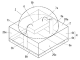
- FIG. 1 is a schematic perspective view of a light emitting device according to Embodiment 1.
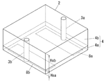
- FIG. 2 is a schematic perspective view of a mounting substrate in the light emitting device of Embodiment 1.
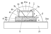
- FIG. 3 is a schematic explanatory diagram of a light traveling path in the light emitting device of the first embodiment. It is explanatory drawing of the relationship between the particle size of an alumina particle, and a reflectance. It is explanatory drawing of the simulation result of the relationship between the thickness of the submount member of the light-emitting device of a comparative example, and light extraction efficiency.
- FIG. 3 is a schematic explanatory diagram of a translucent member in the light emitting device of Embodiment 1.
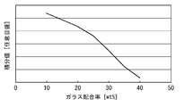
- FIG. 4 is a diagram illustrating the relationship between the glass blending ratio of the translucent member and the integrated intensity of the integrating sphere in the light emitting device of Embodiment 1.
- FIG. 3 is a reflectance-wavelength characteristic diagram of a light transmissive member and an alumina substrate in the light emitting device of Embodiment 1. It is explanatory drawing of the experimental result of the relationship between the particle size of the alumina particle in a 1st light transmission layer with which a light-emitting device is provided, efficiency, and a color difference.
- FIG. 6 is a schematic cross-sectional view showing a modification of the light emitting device of Embodiment 1. It is a schematic perspective view of the LED module provided with the light-emitting device of Embodiment 1.
- FIG. 3 is a reflectance-wavelength characteristic diagram of a light transmissive member and an alumina substrate in the light emitting device of Embodiment 1. It is explanatory drawing of the experimental result of the relationship between the particle size of the
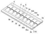
- FIG. 2 shows a light-emitting device of Embodiment 2, wherein (a) is a schematic perspective view, (b) is a schematic cross-sectional view along AA in (a), and (c) is a schematic cross-sectional view along BB in (a).
- 5 is a schematic perspective view of a main part of a light emitting device according to Embodiment 2.
- FIG. It is the schematic perspective view which showed the modification of the light-emitting device of Embodiment 2, and was partly fractured.
- FIG. 6 is a schematic cross-sectional view showing a modification of the light emitting device of Embodiment 2.
- (a) is the schematic perspective view which fractured
- (b) is the principal part enlarged view of (a).
- (a) is the schematic perspective view which fractured
- (b) is the principal part enlarged view of (a).
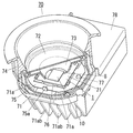
- (a) is the schematic perspective view which shows an example of a lighting fixture provided with the light-emitting device of embodiment.
- the light-emitting device 1 includes a mounting substrate 2, an LED chip 6 bonded to the one surface 20 a side of the mounting substrate 2 via the bonding portion 5, and a seal that covers the LED chip 6 on the one surface 20 a side of the mounting substrate 2. Part 10.
- the mounting substrate 2 includes a translucent member 4, a first through wire 3 a to which a first electrode (not shown) of the LED chip 6 is electrically connected via a first wire 7 a, and a first of the LED chip 6.
- Two electrodes (not shown) are provided with a second through wiring 3b electrically connected via a second wire 7b.
- the translucent member 4 is a member that emits light to the outside by refracting incident light or diffusing (scattering) the light inside.
- the translucent member 4 is formed in a flat plate shape having a plane size larger than the chip size of the LED chip 6.
- the first through wiring 3 a and the second through wiring 3 b are provided in the thickness direction of the translucent member 4.
- the mounting substrate 2 and the sealing portion 10 constitute a package.
- the sealing unit 10 covers the LED chip 6, the first wire 7a, and the second wire 7b.
- the junction 5 can transmit light emitted from the LED chip 6.
- the translucent member 4 includes at least two translucent layers that overlap in the thickness direction of the translucent member 4.
- the translucent member 4 includes two translucent layers (a first translucent layer 4b and a second translucent layer 4a).
- the second light transmissive layer 4a is farther from the LED chip 6 than the first light transmissive layer 4b.
- the first light transmissive layer 4b is closer to the LED chip 6 than the second light transmissive layer 4a.
- the 2nd translucent layer 4a has a higher reflectance with respect to the light radiated
- each of the light transmitting layers 4a and 4b is formed of ceramic. That is, the translucent member 4 includes two ceramic layers 4 a and 4 b that overlap in the thickness direction of the translucent member 4. In the translucent member 4, the ceramic characteristics of the ceramic layers 4 a and 4 b are different from each other, and the ceramic layer 4 a far from the LED chip 6 has a higher reflectance with respect to the light emitted from the LED chip 6.
- the optical characteristics include reflectance, transmittance, absorption rate, and the like.
- the translucent member 4 is composed of at least two ceramic layers that are overlapped in the thickness direction, and the optical characteristics of the ceramic layers are different from each other.
- the ceramic layers farther from the LED chip 6 are more resistant to light emitted from the LED chip 6. What is necessary is just to have a property with a high reflectance.
- the light emitting device 1 emits light from the light emitting layer (not shown) of the LED chip 6, and part of the light that has passed through the LED chip 6 and the joint portion 5 is diffused in the translucent member 4. Therefore, the light that has passed through the LED chip 6 and the joint 5 is less likely to be totally reflected, and is easily extracted from the side surface 20c of the mounting substrate 2 and the one surface 20a. For this reason, in the light-emitting device 1, it becomes possible to improve light extraction efficiency and to improve the total luminous flux.
- the LED chip 6 is provided with a first electrode serving as an anode electrode and a second electrode serving as a cathode electrode on one surface (first surface) 6a side in the thickness direction of the LED chip 6.
- the LED chip 6 includes an LED structure 60 having an n-type semiconductor layer, a light emitting layer, and a p-type semiconductor layer on the main surface 61 a side of the substrate 61.
- the substrate 61 is transparent to the light emitted from the light emitting layer.
- substrate 61 is arrange
- the main surface 61 a of the substrate 61 is a surface on the opposite side of the translucent member 4 (mounting substrate 2) in the substrate 61.
- the LED chip 6 includes the LED structure portion 60 and the substrate 61, and the LED structure portion 60 is disposed on the substrate 61 disposed on the translucent member 4.
- the stacking order of the n-type semiconductor layer, the light-emitting layer, and the p-type semiconductor layer is the n-type semiconductor layer, the light-emitting layer, and the p-type semiconductor layer in order from the side closer to the substrate 61.
- the LED chip 6 preferably has a structure in which a buffer layer is provided between the LED structure 60 and the substrate 61.
- the light emitting layer preferably has a single quantum well structure or a multiple quantum well structure, but is not limited thereto.
- the LED chip 6 may form a double hetero structure with an n-type semiconductor layer, a light emitting layer, and a p-type semiconductor layer.
- the structure of the LED chip 6 is not particularly limited.
- an LED chip having a reflection part such as a Bragg reflector inside may be employed.
- the LED chip 6 is a blue LED chip that emits blue light.
- the blue LED chip employs a gallium nitride-based material as a material of the light emitting layer, and uses a sapphire substrate as the substrate 61.
- the substrate 61 of the LED chip 6 is not limited to the sapphire substrate, but may be any substrate that is transparent to the light emitted from the light emitting layer.
- the chip size of the LED chip 6 is not particularly limited.
- a chip having a chip size of 0.3 mm ⁇ (0.3 mm ⁇ 0.3 mm), 0.45 mm ⁇ , or 1 mm ⁇ can be used.
- the planar shape of the LED chip 6 is not limited to a square shape, and may be, for example, a rectangular shape. When the planar shape of the LED chip 6 is rectangular, the chip size of the LED chip 6 may be, for example, 0.5 mm ⁇ 0.24 mm or 0.5 mm ⁇ 1.0 mm.
- the LED chip 6 does not particularly limit the material of the light emitting layer and the light emission color. That is, the LED chip 6 is not limited to a blue LED chip, and for example, a purple LED chip, an ultraviolet LED chip, a red LED chip, a green LED chip, or the like may be used.
- the material of the joint portion 5 for example, a transparent material such as a silicone resin or an epoxy resin can be employed.
- the LED chip 6 is bonded to the central portion of the mounting substrate 2 on the one surface 20 a side via the bonding portion 5.
- the LED chip 6 is bonded to the central portion on the one surface (first surface) 41 side of the flat light-transmitting member 4 on the mounting substrate 2 via the bonding portion 5.
- the mounting substrate 2 is provided with a first external electrode 8 a and a second external electrode 8 b for supplying power to the LED chip 6 on the other surface (second surface) 42 side of the translucent member 4.
- the first surface 41 and the second surface 42 are orthogonal to the thickness direction of the translucent member 4.
- the first electrode is electrically connected to the first external electrode 8a via the first wire 7a and the first through wiring 3a.
- the second electrode is electrically connected to the second external electrode 8b through the second wire 7b and the second through wiring 3b.
- each of the wires 7a and 7b for example, a gold wire, a silver wire, a copper wire, or an aluminum wire can be employed.
- first external electrode 8a and the second external electrode 8b for example, gold, platinum, molybdenum, tungsten, copper, aluminum, an aluminum alloy, or the like can be employed.
- the first external electrode 8a and the second external electrode 8b may have a single-layer structure or a multilayer structure, but the material on the outermost surface side is preferably gold.
- first through wiring 3a and the second through wiring 3b for example, gold, platinum, molybdenum, tungsten, copper, aluminum, aluminum alloy, or the like can be employed.
- Each of the first through wiring 3a and the second through wiring 3b may be entirely formed of the same material, and a portion formed in the ceramic layer 4b is different from a portion formed in the ceramic layer 4a. It may be formed of a material.
- the translucent member 4 has translucency and diffusibility with respect to light in the ultraviolet wavelength range and visible wavelength range, and as shown schematically by arrows in FIG.
- the light emitted from the light emitting layer of the structure part 60 is transmitted or diffused.
- the translucent member 4 has different optical characteristics of the ceramic layers 4a and 4b, and the ceramic layer 4a far from the LED chip 6 has higher reflectivity with respect to light emitted from the LED chip 6. .
- the light emitting device 1 has the other surface (second surface) 6 b (from the light emitting layer of the LED structure 60 of the LED chip 6 to the thickness direction of the LED chip 6.
- the translucent member 4 can diffuse and reflect the light emitted from the LED chip 6 and incident on the translucent member 4 at the interface between the translucent layers.
- the light emitting device 1 can suppress the light emitted from the LED chip 6 to the light transmissive member 4 side from returning to the LED chip 6, and the other surface (the first surface) of the light transmissive member 4. 2 surface) can be prevented from entering the first external electrode 8a and the second external electrode 8b on the 42 side, and light is transmitted from the one surface (first surface) 41 or the side surface of the translucent member 4. It becomes easy to take out. That is, a part of the light emitted from the light emitting layer of the LED chip 6 to the translucent member 4 side is diffused in the translucent member 4 and the first surface 41 of the translucent member 4 (on the LED chip 6 side). Surface) or from the side.
- the translucent member 4 includes a plurality of translucent layers, and can diffuse and reflect light at the interface between the translucent layers. Therefore, the light emitted from the LED chip 6 and incident on the one surface 20a of the mounting substrate 2 is diffused by the translucent member 4 and suppressed from returning to the LED chip 6, while the one surface 20a (that is, the mounting substrate 2). The light can be extracted from the same surface as the surface on which the light is incident on the mounting substrate 2.
- the light diffused by the translucent member 4 can be extracted not only from one surface 20a of the mounting substrate 2 but also from the side surface 20c of the mounting substrate 2. Therefore, the light emitting device 1 can improve the light extraction efficiency, and reflect the first external electrode 8a, the second external electrode 8b, a circuit board (not shown) on which the light emitting device 1 is mounted, and the like.
- the influence of the rate can be reduced, and the degree of freedom of the material of the first external electrode 8a, the second external electrode 8b and the circuit board can be increased.
- the reflectance of the circuit substrate is likely to change over time, and light extraction There is a concern that the change in efficiency over time will increase.
- the light emitting device 1 according to the present embodiment it is possible to reduce the influence of the reflectance of the circuit board on the light extraction efficiency, and it is possible to suppress the temporal change of the light extraction efficiency.
- the translucent member 4 has a rectangular shape in plan view, but is not limited thereto, and may be, for example, a circular shape or a polygonal shape other than a rectangular shape.
- the planar size of the translucent member 4 is set larger than the planar size of the LED chip 6. Thereby, the light emitting device 1 can improve the light extraction efficiency.
- the one surface 20 a of the mounting substrate 2 is formed by the first surface 41 of the translucent member 4.
- the translucent member 4 is configured to have a linear expansion coefficient close to that of the LED chip 6, thereby reducing the stress acting on the LED chip 6 due to the difference in linear expansion coefficient between the LED chip 6 and the circuit board. It preferably has a relaxation function. Thereby, the light emitting device 1 can relieve the stress acting on the LED chip 6 due to the difference in the linear expansion coefficient between the LED chip 6 and the circuit board.
- the translucent member 4 has a heat conduction function for conducting heat generated in the LED chip 6 to a circuit board or the like disposed on the other surface (second surface) 42 side of the translucent member 4. Preferably it is. Moreover, it is preferable that the translucent member 4 has a heat conduction function for conducting heat generated in the LED chip 6 in a range wider than the chip size of the LED chip 6. Thereby, the light emitting device 1 can efficiently dissipate the heat generated in the LED chip 6 through the translucent member 4.
- the sealing part 10 is formed from a material including a transparent material and a phosphor.
- the phosphor is a phosphor that is excited by light emitted from the LED chip 6 and emits light of a color different from that of the LED chip 6.
- the transparent material of the sealing portion 10 for example, a silicone resin, an epoxy resin, an acrylic resin, glass, an organic / inorganic hybrid material in which an organic component and an inorganic component are mixed and bonded at the nm level or the molecular level, and the like are adopted. Can do.
- the phosphor of the sealing unit 10 functions as a wavelength conversion material that converts light emitted from the LED chip 6 into light having a longer wavelength than the light. Thereby, the light emitting device 1 can obtain mixed color light of the light emitted from the LED chip 6 and the light emitted from the phosphor.
- the light emitting device 1 employs a blue LED chip as the LED chip 6 and a yellow phosphor as the phosphor of the wavelength conversion material, white light can be obtained. That is, the light emitting device 1 can emit the blue light emitted from the LED chip 6 and the light emitted from the yellow phosphor from the LED chip 6 or the translucent member 4 and obtain white light. .
- the phosphor that is the wavelength conversion material is not limited to the yellow phosphor, and for example, a yellow phosphor and a red phosphor, or a red phosphor and a green phosphor may be employed. Further, the phosphor as the wavelength conversion material is not limited to one type of yellow phosphor, and two types of yellow phosphors having different emission peak wavelengths may be employed. The light emitting device 1 can improve color rendering by adopting a plurality of types of phosphors as the wavelength conversion material.
- the light-emitting device 1 preferably has a semispherical shape for the sealing portion 10, thereby suppressing color unevenness.
- the sealing portion 10 has a hemispherical shape, but is not limited thereto, and may be a semi-elliptical spherical shape or a semi-cylindrical shape, for example.
- the light emitting device 1 may have a configuration in which the sealing unit 10 contains a light diffusing material.
- the light diffusing material is in the form of particles and is preferably dispersed in the sealing portion 10.
- the light emitting device 1 can further suppress the color unevenness because the sealing portion 10 contains a light diffusing material.
- the light diffusing material include inorganic materials such as aluminum oxide, silica, titanium oxide, and Au, organic materials such as fluorine-based resins, and organic materials in which organic components and inorganic components are mixed and combined at the nm level or molecular level. ⁇ Inorganic hybrid materials can be used.
- the light-emitting device 1 reduces the content rate of the light diffusing material necessary for obtaining an effect of suppressing the same level of color unevenness as the difference in refractive index between the light diffusing material and the transparent material of the sealing portion 10 increases. Is possible.
- the LED chip 6 is a blue LED chip and the sealing unit 10 includes a plurality of types of phosphors (green phosphor and red phosphor) and a light diffusing material, Color rendering can be further improved.
- the LED chip 6 is an ultraviolet LED chip, and the sealing unit 10 includes a plurality of types of phosphors (blue phosphor, green phosphor, red phosphor) and a light diffusing material. If so, color rendering can be further improved.
- the translucent member 4 will be described in more detail.
- the uppermost translucent layer (ceramic layer) 4b closest to the LED chip 6 is replaced with the first translucent layer (first ceramic layer) 4b.
- the light-transmitting layer (ceramic layer) 4a that is the lowest layer farthest from the LED chip 6 may be referred to as a second light-transmitting layer (second ceramic layer) 4a. That is, when the translucent member 4 includes three or more translucent layers, the first translucent layer 4b is the layer closest to the LED chip 6, and the second translucent layer 4a is farthest from the LED chip 6. Is a layer.
- the first light transmissive layer 4b is preferably made of a material having a high transmittance of light emitted from the LED chip 6 and a refractive index close to the refractive index of the LED chip 6. That the refractive index of the first light transmissive layer 4b is close to the refractive index of the LED chip 6 means that the difference between the refractive index of the first light transmissive layer 4b and the refractive index of the substrate 61 in the LED chip 6 is 0.1 or less. This means that there is a difference in refractive index of 0.
- the first light transmissive layer 4b is preferably made of a material having high heat resistance.
- the first light transmissive layer 4b is a ceramic layer in the first embodiment.
- alumina Al 2 O 3
- the 1st ceramic layer 4b can be comprised with an alumina substrate, for example.
- the particle diameter of the alumina particles is preferably 1 ⁇ m to 30 ⁇ m.
- the first ceramic layer 4b can reduce the reflectance when the particle diameter of the alumina particles is large, and can increase the scattering effect when the particle diameter of the alumina particles is small. In short, there is a trade-off relationship between reducing the reflectance and increasing the scattering effect.
- the above-mentioned particle size is a value obtained from a number-based particle size distribution curve.
- the number-based particle size distribution curve is obtained by measuring the particle size distribution by an image imaging method. Specifically, the SEM image is obtained by observing with a scanning electron microscope (SEM), This is obtained from the size (biaxial average diameter) and the number of particles obtained by image processing of the SEM image.
- SEM scanning electron microscope
- the particle size value when the integrated value is 50% is called the median diameter (d 50 )
- the above-mentioned particle size means the median diameter.
- the relationship between the particle size of the spherical alumina particles on the alumina substrate and the reflectance is as shown in FIG. 5, and the reflectance increases as the particle size decreases.
- the relationship between the median diameter (d 50 ) of the first ceramic layer 4b and the measured value of the reflectance was substantially the same as the theoretical value of FIG.
- the measured value of reflectance is a value measured using a spectrophotometer and an integrating sphere.
- the material of the first light transmissive layer 4b is not limited to ceramic, and for example, glass, SiC, GaN, GaP, sapphire, epoxy resin, silicone resin, unsaturated polyester, or the like may be employed.
- the ceramic material is not limited to Al 2 O 3 , but may be other metal oxides (eg, magnesia, zirconia, titania), metal nitride (eg, aluminum nitride).
- the material of the first light transmissive layer 4b is preferably ceramic rather than single crystal from the viewpoint of forward scattering of the light emitted from the LED chip 6.
- Lumicera registered trademark
- Hi-Serum product name of NGK Co., Ltd.
- High serum is a translucent alumina ceramic.
- the first light transmissive layer 4b preferably has a particle size of about 1 ⁇ m to 5 ⁇ m.
- the first light-transmitting layer 4b may be formed by forming a void, a modified portion with a changed refractive index, or the like inside the single crystal.
- the voids and modified portions can be formed, for example, by condensing and irradiating laser light from a femtosecond laser to the formation regions of the voids and modified portions in the single crystal.
- the wavelength of the laser beam of the femtosecond laser, the irradiation conditions, and the like may be changed as appropriate depending on the material of the single crystal, the formation target (gap, modified portion), the size of the formation target, and the like.
- the first light-transmitting layer 4b is made of a base resin (for example, epoxy resin, silicone resin, unsaturated polyester, etc.) and a filler having a refractive index different from that of the base resin (hereinafter referred to as “first base resin”). (Hereinafter referred to as “first filler”) may also be included.
- the first filler preferably has a smaller refractive index difference from the first base resin.
- the first filler preferably has a higher thermal conductivity.
- the first light transmissive layer 4b preferably has a higher filling density of the first filler from the viewpoint of increasing the thermal conductivity.
- the shape of the first filler is preferably spherical from the viewpoint of suppressing total reflection of incident light.
- the first filler has less reflection and refraction as the particle size is larger.
- the first light transmissive layer 4b has a first filler having a relatively large particle diameter on the side close to the LED chip 6 in the thickness direction of the first light transmissive layer 4b, and is relatively on the side far from the LED chip 6. You may comprise so that there may be a 1st filler with a small particle size. In this case, you may comprise the 1st translucent layer 4b by multilayering the several layer from which the particle size of a 1st filler mutually differs.
- Radiation from the LED chip 6 toward the translucent member 4 is performed around the LED chip 6 mounting area in the surface of the first translucent layer 4b on the LED chip 6 side (the first surface 41 of the translucent member 4).
- a fine concavo-convex structure portion for suppressing the total reflection of the light reflected or refracted inside the translucent member 4 is formed.
- the concavo-convex structure portion may be formed by roughening the surface of the first light transmissive layer 4b by, for example, sandblasting.
- the surface roughness of the concavo-convex structure portion for example, the arithmetic average roughness Ra defined by JIS B 0601-2001 (ISO 4287-1997) is preferably about 0.05 ⁇ m.
- the translucent member 4 forms a resin layer having a refractive index smaller than that of the first translucent layer 4b around the mounting region of the LED chip 6 on the surface of the first translucent layer 4b on the LED chip 6 side. You may adopt what you did.
- a material for the resin layer for example, a silicone resin, an epoxy resin, or the like can be employed.
- a resin containing a phosphor may be used.
- the second translucent layer 4a is translucent to the light emitted by the LED chip.
- the second light transmissive layer 4a is a ceramic layer.
- the second light transmissive layer 4 a diffuses and reflects the light emitted from the LED chip 6. That is, the second light transmissive layer 4a is preferably configured to diffusely reflect the light radiated from the LED chip 6 rather than the light transmissive layer 4a.
- the second ceramic layer (second translucent layer) 4a for example, a material having a higher refractive index than SiO 2 , Al 2 O 3 and Al 2 O 3 (for example, ZrO 2 or TiO 2 ) and CaO are used. And a composite material containing BaO as components can be employed.
- the second ceramic layer 4a preferably has an Al 2 O 3 particle size of 0.1 ⁇ m to 1 ⁇ m.
- the second ceramic layer 4a can adjust optical characteristics (reflectance, transmittance, absorptivity, etc.) by adjusting the components, composition, particle size, thickness, and the like of the composite material.
- the translucent member 4 may have a grain size of the first ceramic layer 4b larger than that of the second ceramic layer 4a. .
- the material of the second light transmissive layer 4a is not limited to ceramic, and for example, glass, SiC, GaN, GaP, sapphire, epoxy resin, silicone resin, unsaturated polyester, or the like may be employed.
- the ceramic material is not limited to Al 2 O 3 , but may be other metal oxides (eg, magnesia, zirconia, titania), metal nitride (eg, aluminum nitride).
- both the 1st translucent layer 4b and the 2nd translucent layer 4a are formed with a semiconductor (SiC, GaN, GaP, etc.), it is between 1st translucent layer 4b and the 2nd translucent layer 4a.
- a semiconductor SiC, GaN, GaP, etc.
- the second light transmissive layer 4a preferably has a particle size of 1 ⁇ m or less, more preferably about 0.1 ⁇ m to 0.3 ⁇ m.
- the 2nd translucent layer 4a can be comprised by the below-mentioned porous layer 4a, for example.
- the first light transmissive layer 4b was constituted by the first ceramic layer 4b made of alumina having a purity of 99.5%, the bulk density was 3.8 to 3.95 g / cm 3 . Further, when the first light transmissive layer 4b was constituted by the first ceramic layer 4b made of alumina having a purity of 96%, the bulk density was 3.7 to 3.8 g / cm 3 .
- the second transparent layer 4a when constituted by a porous layer 4a, bulk density was 3.7 ⁇ 3.8g / cm 3.
- the above-described bulk density is a value estimated by observing with an SEM, obtaining an SEM image, and performing image processing on the SEM image.
- the second light transmissive layer 4a may be formed by forming a void, a modified portion in which the refractive index is changed, or the like inside the single crystal.
- the voids and modified portions can be formed, for example, by condensing and irradiating laser light from a femtosecond laser to the formation regions of the voids and modified portions in the single crystal.
- the wavelength of the laser light of the femtosecond laser, the irradiation conditions, and the like may be appropriately changed depending on the material of the single crystal, the object to be formed (gap, modified portion), the size of the object to be formed, and the like.
- the second light transmissive layer 4a is made of a base resin (for example, epoxy resin, silicone resin, unsaturated polyester, fluororesin, etc.) and a refractive index of the base resin (hereinafter referred to as “second base resin”). Of different fillers (hereinafter referred to as “second filler”).
- the second light transmissive layer 4a has a second filler having a relatively large particle diameter on the side close to the LED chip 6 in the thickness direction of the second light transmissive layer 4a, and is relatively on the side far from the LED chip 6. You may comprise so that there may be a 2nd filler with a small particle size.
- the material of the second filler for example, white inorganic materials are preferred, for example, can be employed metal oxides such as TiO 2 or ZnO.
- the particle size of the second filler is preferably about 0.1 ⁇ m to 0.3 ⁇ m, for example.
- the filling rate of the second filler is preferably about 50 to 75 wt%, for example.
- the silicone resin of the second base resin for example, methyl silicone or phenyl silicone can be employed.
- the second filler preferably has a larger refractive index difference from the second base resin.
- KER-3200-T1 manufactured by Shin-Etsu Chemical Co., Ltd. can be used as a material containing the second filler in the second base resin.
- the second filler core-shell particles or hollow particles can be employed.
- the refractive index of the core can be arbitrarily set, but is preferably smaller than the refractive index of the second base resin.
- the hollow particles are preferably gas (for example, air, inert gas) or a vacuum inside and have a refractive index smaller than that of the second base resin.
- the second light transmissive layer 4a may be composed of a light diffusion sheet.
- a white polyethylene terephthalate sheet containing a large number of bubbles can be employed.
- the light-transmitting member 4 is pre-sintered with a ceramic green sheet of the first light-transmitting layer 4b. After the formation of the first light transmissive layer 4b, the ceramic green sheet of the second light transmissive layer 4a can be superimposed on the first light transmissive layer 4b and sintered.
- the translucent member 4 when the second translucent layer 4 a includes bubbles, the first translucent layer 4 b may also include bubbles. However, the first translucent layer 4 b has the second translucent layer. It is preferable that the number of bubbles is smaller than that of the optical layer 4a and the bulk density is large.
- the first light-transmitting layer 4b and the second light-transmitting layer 4a are preferably materials that are highly resistant to light and heat from the LED chip 6 and the phosphor.
- the light emitting device 1 may include a reflective layer that reflects light from the LED chip 6 or the like on the second surface 42 side of the translucent member 4.
- a reflective layer that reflects light from the LED chip 6 or the like on the second surface 42 side of the translucent member 4.
- a material for the reflective layer silver, aluminum, a silver-aluminum alloy, other silver alloys, aluminum alloys, or the like can be employed.
- the reflective layer can be composed of, for example, a thin film, metal foil, solder resist (solder), or the like.
- the first external electrode 8 a and the second external electrode 8 b are formed on the other surface (second surface) 42 of the translucent member 4, and then the first penetration in the translucent member 4.
- the first through wiring 3a and second through wiring 3b are formed.
- the first through wiring 3a and the second through wiring 3b are preferably formed before the step of dividing the mounting substrate 2 into individual pieces.
- the inventors of the present application have the LED chip 6 bonded to the submount member via the first bonding portion, and the submount member has the second bonding portion.
- An LED module is assumed in which the submount member is composed of only a single-layer alumina substrate.
- the inventors of the present application simulated the light extraction efficiency of the light emitting device of this comparative example using the dimension of the submount member in the light emitting device of this comparative example as a parameter. As a result, the results shown in FIG. 6 were obtained. It was.
- This simulation is a geometric optical simulation based on a ray tracing method using the Monte Carlo method.
- the reflectance of the one surface of the opaque substrate was 95% and the absorptivity of the opaque substrate was 5%.
- the chip size of the LED chip 6 is 0.5 mm ⁇ 0.24 mm.
- the material of the LED chip 6 was sapphire having a refractive index of 1.77, and the material of the LED structure 60 was GaN having a refractive index of 2.5.
- the material of the LED structure 60 was GaN having a refractive index of 2.5.
- the light emitting layer it was assumed that light having an isotropic and uniform intensity in all directions was radiated from all points of the light emitting layer.
- the material of a 1st junction part and a 2nd junction part it was set as the silicone resin whose refractive index is 1.41.
- the horizontal axis represents the thickness of the submount member
- the vertical axis represents the light extraction efficiency
- “B1” in the figure represents “B2” in the figure when the planar size of the submount member is 1 mm ⁇ .
- FIG. 6 also shows that when the thickness of the submount member is 2 mm or less, the light extraction efficiency is improved when the planar size of the submount member is smaller.
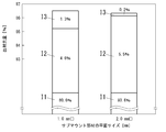
- the inventors of the present invention have compared the light emitting device of the comparative example with respect to each of the thickness of the submount member made only of the alumina substrate being 0.4 mm and the plane size being 1 mm ⁇ and 2 mm ⁇ .
- the result shown in FIG. 7 was obtained as an example.
- This simulation is a geometric optical simulation based on a ray tracing method using the Monte Carlo method. In this simulation, it was assumed that the reflectance of the one surface of the opaque substrate was 95% and the absorptivity of the opaque substrate was 5%. In this simulation, it is assumed that the chip size of the LED chip 6 is 0.5 mm ⁇ 0.24 mm. In this simulation, it is assumed that only the Fresnel loss occurs on the side surface of the LED chip 6.
- “I1” in FIG. 7 is the ratio of the amount of light emitted from the LED chip 6. Further, “I2” in FIG. 7 is a ratio of the amount of light emitted from the exposed surface on the LED chip 6 side of the submount member. Further, “I3” in FIG. 7 is the ratio of the amount of light emitted from the side surface of the submount member.
- the inventors of the present application can improve the light extraction efficiency because the ratio of the amount of light emitted from the side surface of the submount member increases as the planar size of the submount member decreases. I got the knowledge that it would be possible.
- the inventors of the present application have examined the relationship between the thickness of the submount member and the luminous flux emitted from the light emitting device of the comparative example, with the planar size of the submount member being 2 mm ⁇ for various opaque substrates. .
- the luminous flux was measured with an integrating sphere.
- the inventors of the present application obtained the experimental results shown in FIG. In this experiment, a blue LED chip in which the substrate was a sapphire substrate and the emission peak wavelength of the light emitting layer was 460 nm was adopted as the LED chip 6.
- the chip size of the LED chip 6 is 0.5 mm ⁇ 0.24 mm.
- the sealing part 10 consists of a silicone resin and yellow fluorescent substance.
- the white circle (O) on C1 in FIG. 8 shows the light emission of Reference Form 1 using an alumina substrate as a submount member and a silver substrate having a reflectance of 98% for light having a wavelength of 460 nm as an opaque substrate. This is a measurement of the luminous flux for the device.
- the white triangle ( ⁇ ) on C2 in FIG. 8 uses an alumina substrate as a submount member, and a white surface having a reflectance of 92% for light having a wavelength of 460 nm on the surface of a copper substrate as an opaque substrate. It is the measured value of the light beam regarding the light-emitting device of the reference form 2 using what provided the reflective layer which consists of resists.
- the white diamond ( ⁇ ⁇ ) on C3 in FIG. 8 uses an alumina substrate as a submount member, and a reference form using an aluminum substrate having a reflectance of 95% for light having a wavelength of 460 nm as a non-transparent substrate.
- 3 is a measured value of the luminous flux for the light emitting device 3.
- the light emitting device 1 of the present embodiment can improve the light extraction efficiency by increasing the thickness of the translucent member 4 corresponding to the submount member.
- the translucent member 4 from the viewpoint of efficiently transferring the heat generated in the LED chip 6 to the second surface (other surface) 42 side of the translucent member 4 (that is, from the viewpoint of improving heat dissipation), the translucent member 4.
- the thickness of is preferably smaller. In short, light extraction efficiency and heat dissipation are in a trade-off relationship.
- the inventors of the present application manufactured a light emitting device having a reference structure using a high-purity alumina substrate as a non-transparent substrate without providing a submount member, and measuring the light flux of the light emitting device having the reference structure.
- the experiment was conducted.
- Black squares ( ⁇ ) in FIG. 8 are measured values of light fluxes related to the light emitting device having the reference structure.
- the inventors of the present application obtained an experimental result that the thickness of the submount member from which the light beam equal to or larger than the light beam of the light emitting device having the reference structure is obtained is 0.4 mm or more. .
- the inventors of the present invention can set the thickness of the submount member in the range of about 0.4 mm to 0.5 mm in consideration of light extraction efficiency and heat dissipation in the light emitting device of the comparative example. I thought it was preferable.
- the alumina substrate used in the light emitting device having the reference structure had a thickness of 1 mm, a particle size of 1 ⁇ m, and a reflectance of 91%.
- the translucent member 4 is configured to include the second ceramic layer 4a and the first ceramic layer 4b that overlap in the thickness direction.
- the inventors of the present application use a translucent member 4 in place of the submount member of the light emitting device of Reference Embodiment 2, set the thickness of the translucent member 4 to 0.5 mm, and the thickness Hsa of the second ceramic layer 4a. (See FIG. 3) is 0.1 mm, the reflectance of the second ceramic layer 4a with respect to light having a wavelength of 450 nm is 96%, the thickness Hsb (see FIG. 3) of the first ceramic layer 4b is 0.4 mm, and the first ceramic.
- An experiment for measuring the luminous flux was performed on the light emitting device of Reference Embodiment 4 in which the reflectance of the layer 4b with respect to light having a wavelength of 450 nm was 80%.
- the measured value of the luminous flux is the measured value of the luminous flux. It can be seen from FIG. 8 that the luminous flux of the light emitting device of Reference Mode 4 is improved as compared with the light emitting device of the reference structure. Further, from FIG. 8, it is estimated that in the light emitting device of the reference form 4, it is possible to improve the luminous flux as compared with the case where the thickness of the submount member is 0.5 mm in each of the reference forms 1, 2, and 3. The In addition, regarding the translucent member 4 used in the light-emitting device of Reference Form 4, the light absorption rate at 450 nm was approximately 0% when measured using an integrating sphere and a spectrophotometer.
- the translucent member 4 used in the light-emitting device of Reference Form 4 the reflectance of light at 450 nm was approximately 94% when measured using an integrating sphere and a spectrophotometer.
- the single-layer alumina substrate having a thickness of 0.4 mm in Reference Embodiments 1, 2, and 3 the reflectance of light at 450 nm was measured using an integrating sphere and a spectrophotometer, and was approximately 89. %Met.
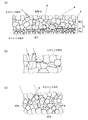
- the principle that the light extraction efficiency of the light-emitting device 1 is improved will be described with reference to FIGS. 9 and 10 (a), (b), and (c). Even if the estimation mechanism is different, it is within the scope of the present invention.
- the light emitting device 1 is disposed on one surface 2sa of the wiring board 21 to be described later, but may not be disposed on the wiring board 21.
- FIGS. 9 and 10 schematically show the traveling path of the light emitted from the light emitting layer of the LED structure 60 of the LED chip 6.
- Is. 9 and the solid line arrows in FIGS. 10A and 10B schematically show the traveling path of the light emitted from the light emitting layer and reflected by the first surface 41 of the translucent member 4.
- the broken-line arrows are emitted from the light-emitting layer of the LED structure 60 and enter the translucent member 4.
- the traveling path of light is schematically shown.
- the inventors of the present application in the first ceramic layer 4 b, the difference in refractive index between the ceramic particles and the grain boundary phase (glass component is the main component). Therefore, it was estimated that reflection and refraction occurred at the interface between the ceramic particles and the grain boundary phase. Further, as shown in FIG. 9 and FIG. 10C, the inventors of the present application have a difference in the refractive index between the ceramic particles and the pores or grain boundary phase (the glass component is the main component) in the second ceramic layer 4 a. As a result, it was estimated that reflection and refraction occurred at the interface between the ceramic particles and the pores or grain boundary phase. Further, as shown in FIG. 9 and FIG.
- the inventors of the present application in the second ceramic layer 4a, caused the difference between the pores and the grain boundary phase due to the refractive index difference between the pores and the grain boundary phase. It was estimated that reflection and refraction occurred at the interface.
- the ceramic plate material the inventors of the present invention, if the plate thickness is the same, the larger the particle size of the ceramic particles, the fewer the number of interfaces, and the case where the ceramic particles and Since the probability of passing through the interface with the grain boundary phase is reduced, it is estimated that the reflectance is reduced and the transmittance is increased.
- the inventors of the present application can improve the light extraction efficiency of the light emitting device 1 by transmitting the light emitted from the LED chip 6 as much as possible in the first ceramic layer 4b and reflecting it as much as possible in the second ceramic layer 4a. I guessed it. For this reason, in the translucent member 4, it is preferable that the first ceramic layer 4b and the second ceramic layer 4a have a relatively large particle size of ceramic particles in the first ceramic layer 4b, and the second ceramic layer 4a. It is preferable that the ceramic particles have a relatively small particle size and the second ceramic layer 4a includes pores.
- the first ceramic layer 4b is a first dense layer 4b made of ceramics fired at a high temperature of about 1500 ° C. to 1600 ° C.
- the first ceramic layer 4b has ceramic particles firmly bonded to each other by high-temperature firing, and has better rigidity than the second ceramic layer 4a.
- good rigidity means that the bending strength is relatively high.
- alumina is preferable as a material of the first ceramic layer 4b.
- the second ceramic layer 4a is a ceramic fired at 1000 ° C. or lower (for example, 850 ° C. to 1000 ° C.), which is a relatively low temperature compared to the first ceramic layer 4b.
- the ceramic constituting the second ceramic layer 4a is, for example, a second dense layer 4a containing a ceramic filler (fine particles) and a glass component, or a porous layer 4a containing a ceramic filler (fine particles) and a glass component. be able to.
- the second light transmitting layer (second ceramic layer) 4a is fired at a lower temperature than the first light transmitting layer (first ceramic layer) 4b.
- the 1st translucent layer 4b is baked at 1500 degreeC or more and 1600 degrees C or less
- the 2nd translucent layer 4a is baked at 850 degreeC or more and 1000 degrees C or less.
- the second dense layer 4a is a ceramic in which fine particles of the ceramic filler are bonded by sintering, and the glass component is arranged in a matrix around the ceramic filler to form a dense ceramic.
- the ceramic filler mainly exhibits a light reflecting function.
- a material in which a ceramic filler is mixed with glass ceramics containing borosilicate glass, zinc borosilicate glass and alumina, glass ceramics containing soda lime glass and alumina, or the like can be used.
- the glass content contained in the glass ceramic is preferably set in the range of about 35 to 60 wt%.
- the content of the ceramic contained in the glass ceramic is preferably set in the range of about 40 to 60 wt%.
- the second dense layer can also increase the refractive index of the glass ceramic by replacing the zinc component of the borosilicate glass with titanium oxide or tantalum oxide.
- the material of the ceramic filler is preferably a material having a higher refractive index than glass ceramics, for example, tantalum pentoxide, niobium pentoxide, titanium oxide, barium oxide, barium sulfate, magnesium oxide, calcium oxide, strontium oxide, zinc oxide, Zirconium oxide, silicate oxide (zircon), or the like can be used.
- the second ceramic layer 4a is composed of a porous layer (hereinafter, the second ceramic layer 4a is also referred to as a porous layer 4a), as shown in the schematic diagram of FIG. 11, a porous material having a large number of pores 40c.
- the first glass layer 40aa is interposed between the porous layer 4a and the first ceramic layer 4b, and the second glass layer 40ab is laminated on the opposite side of the porous layer 4a from the first ceramic layer 4b side. preferable.
- the porous layer 4a has a higher reflectance than the first light transmitting layer 4b.
- the glass layers 40aa and 40ab are formed so as not to diffuse light at the interface between layers or within the layer. Therefore, the first glass layer 40aa and the second glass layer 40ab do not correspond to the light transmitting layer in the present embodiment. Therefore, in FIG. 11, the porous layer 4a is the second light transmitting layer 4a.
- the porosity of the porous layer 4a is set to about 40%, but is not particularly limited.
- Each of the first glass layer 40aa and the second glass layer 40ab is a transparent layer made of a glass component and transmits visible light. Although the thickness of the 1st glass layer 40aa and the 2nd glass layer 40ab should just be set to about 10 micrometers, for example, it does not specifically limit.
- Each glass component of the first glass layer 40aa and the second glass layer 40ab are both but about half is composed of SiO 2, it is not particularly limited.
- the first glass layer 40aa is disposed so as to be interposed between the porous layer 4a and the first ceramic layer 4b, and is in close contact with the surface of the porous layer 4a and the surface of the first ceramic layer 4b by firing during manufacturing. ing.
- the second glass layer 40ab is disposed on the opposite side of the porous layer 4a from the first ceramic layer 4b side, and protects the porous layer 4a. Accordingly, the pores 40c existing on the surface of the porous layer 4a opposite to the first ceramic layer 4b side are sealed by the second glass layer 40ab.
- the porous layer 4a includes a ceramic filler (fine particles) and a glass component.
- ceramic filler particles are bonded together by sintering to form a cluster, and a porous structure is formed.
- the glass component serves as a binder for the ceramic filler.
- the ceramic filler and a large number of pores exhibit the main light reflecting function.
- the method for forming the porous layer 4a can be formed according to, for example, paragraphs [0023] to [0026] of WO 2012/039442 and the package manufacturing process disclosed in FIG. .
- the porous layer 4a can change the reflectance by changing the weight ratio of the glass component and the ceramic component (alumina, zirconia, etc.), for example. That is, the reflectance of the porous layer 4a can be changed by changing the glass blending ratio.
- FIG. 12 is a result of measuring reflected light when light is incident from a standard light source on one surface side in the thickness direction of the porous layer 4a, where the horizontal axis is the glass blending ratio and the vertical axis is the integrated intensity by the integrating sphere. is there. In the integrating sphere, reflected light having a wavelength of 380 to 780 nm was integrated. From FIG. 12, it can be seen that the reflectance can be increased by lowering the glass blending ratio.
- the first ceramic layer 4b is formed by firing alumina at 1600 ° C., and the porous layer 4a is blended so that the weight ratio of the glass component and the ceramic component is 20:80. It is formed by firing the material at 850 ° C.
- borosilicate glass having a median diameter of about 3 ⁇ m is used as a glass component
- alumina having a median diameter of about 0.5 ⁇ m and a median diameter of about 2 ⁇ m is used as a zirconia.
- the median diameter is about 0.2 ⁇ m.
- the thickness of the first ceramic layer 4b is 0.38 mm
- the thickness of the porous layer 4a is 0.10 mm.
- the reflectance-wavelength characteristics of the translucent member 4 in the example are as indicated by A3 in FIG. 13, and the reflectance-wavelength characteristics of a single layer alumina substrate having a thickness of 0.38 mm are shown in FIG. It was as shown in A4.
- the weight ratio between the glass component and the ceramic component in the porous layer 4a and the particle size of each material are not particularly limited.
- the porous layer 4a has a gradient composition in which the glass component concentration gradually decreases from both sides in the thickness direction to the inside when the glass components of the first glass layer 40aa and the second glass layer 40ab penetrate during manufacturing. is doing.
- the glass occupies an area of 70% or more, and there is a dense layer of glass.
- the glass occupies an area of about 20% per unit area, and the glass and the ceramic filler are at a certain ratio to each other. There are sparse mixed layers.
- the inventors of the present application relate to the light emitting device 1 by varying the particle diameter (median diameter) of the alumina particles in the first ceramic layer 4b, and measuring the luminous flux and chromaticity of each light emitting device 1.
- An experiment was conducted.
- a blue LED chip in which the substrate was a sapphire substrate and the emission peak wavelength of the light emitting layer was 460 nm was adopted as the LED chip 6.
- the chip size of the LED chip 6 is 0.5 mm ⁇ 0.24 mm.
- the submount member 4 had a thickness of 0.49 mm and a planar size of 2 mm ⁇ (2 mm ⁇ 2 mm).
- the chromaticity is a psychophysical property of a color determined by chromaticity coordinates (chromaticity coordinates) in the xy chromaticity diagram (chromaticity diagram) of the CIE color system.
- chromaticity the direction in which the emission angle of light emitted from the light emitting device 1 is 0 ° (optical axis direction), and the direction in which the emission angle is 60 ° (direction in which the angle with the optical axis is 60 °), respectively. was measured.
- the spectral distribution at each radiation angle was obtained with a spectrophotometer, and the chromaticity of the CIE color system was calculated from each spectral distribution.
- FIG. 14 summarizes the results of the experiment.
- the horizontal axis in FIG. 14 is the particle size.
- the vertical axis on the left side of FIG. 14 represents the efficiency obtained from the light flux and the input power to the light emitting device 1.
- the vertical axis on the right side of FIG. 14 is the color difference.
- the color difference is the chromaticity in the direction in which the radiation angle is 60 °, based on the value of x of the chromaticity coordinates in the direction in which the radiation angle is 0 ° (hereinafter referred to as “x 0 ”). It is an increase / decrease value of the value of coordinates x (hereinafter referred to as “x 1 ”). That is, the color difference on the vertical axis on the right side of FIG.
- the 14 is a value of (x 1 ⁇ x 0 ).
- the value of (x 1 ⁇ x 0 ) is a positive value, the larger the absolute value, the more chromaticity is shifted to the yellowish white side. Further, when the value of (x 1 ⁇ x 0 ) is a negative value, it means that the chromaticity is shifted to the bluish white side as the absolute value is larger.
- the design value of the chromaticity of the light emitting device 1 is (0.33, 0.33). That is, the design value of x of the chromaticity coordinates is 0.33.
- the design value of chromaticity is an example and is not particularly limited.
- the black rhombus ( ⁇ ) in FIG. 14 is an actual measurement value of the efficiency of the light emitting device 1. Further, black squares ( ⁇ ) in FIG. 14 are measured values of the color difference of the light emitting device 1. In addition, white rhombuses ( ⁇ ) in FIG. 14 are measured values of the efficiency of the light emitting device having the above-described reference structure. Further, white squares ( ⁇ ) in FIG. 14 are measured values of the color difference of the light emitting device having the above-described reference structure. Since the light emitting device having the reference structure does not include the submount member 4, the particle size on the horizontal axis in FIG. 14 is the particle size of the alumina substrate.
- the allowable range of the color difference of the light emitting device 1 is, for example, from ⁇ 0.0015 to 0.0015 from the viewpoint of suppressing color unevenness and realizing a color difference equal to or less than the color difference of the light emitting device having the reference structure. A range is preferred.
- FIG. 14 shows that the efficiency of the light-emitting device 1 is improved as compared with the light-emitting device having the reference structure. Further, from FIG. 14, in the light emitting device 1, by setting the particle diameter in the range of 1 ⁇ m to 4 ⁇ m, it is possible to suppress the color difference from exceeding the allowable range (in other words, larger than the color difference of the light emitting device having the reference structure). However, it is considered that the efficiency can be improved as compared with the light emitting device having the reference structure.
- the translucent member 4 is composed of two translucent layers (ceramic layers) 4a and 4b, and the optical characteristics of the ceramic layers 4a and 4b are different from each other and far from the LED chip 6.
- the ceramic layer 4 a has a higher reflectance with respect to light emitted from the LED chip 6 than the ceramic layer 4 b close to the LED chip 6.
- the light-emitting device 1 of this embodiment can improve light extraction efficiency compared with the case where the translucent member 4 is comprised only by the single layer alumina substrate.
- the light absorptivity (approximately 0%) in the translucent member 4 is lower than the light absorptivity (for example, about 2 to 8%) in the non-transparent substrate.
- Part of the light incident on the one surface of the translucent member 4 may be scattered within the ceramic layer 4b or reflected at the interface between the ceramic layer 4b and the ceramic layer 4a. It becomes possible. Therefore, the light-emitting device 1 can reduce the light transmitted through the translucent member 4 and emitted from the other surface of the translucent member 4, so that the first external electrode 8 a, the second external electrode 8 b, Absorption loss in the circuit board can be reduced, and the light extraction efficiency can be improved.
- the first ceramic layer 4b and the second ceramic layer 4a relatively increase the light transmittance of the first ceramic layer 4b, and the second ceramic layer 4a The light scattering rate is increased.
- the light emitting device 1 can diffuse light with the second ceramic layer 4a far from the LED chip 6, and is diffused before reaching the circuit board as compared with the case of only the first ceramic layer 4b. It is assumed that there will be more light.
- the light-emitting device 1 has a high possibility that the light reflected by the circuit board directly under the translucent member 4 is diffused without returning to the LED chip 6.
- the light emitting device 1 when the translucent member 4 is configured only by the second ceramic layer 4 a, light emitted from the LED chip 6 toward the translucent member 4 may be scattered near the LED chip 6. Therefore, it is considered that the possibility that the light scattered near the LED chip 6 returns to the LED chip 6 is increased. Therefore, it is assumed that the light emitting device 1 can reduce the light returning to the LED chip 6 as compared with the case where the translucent member 4 is only the second ceramic layer 4a. Further, in the light emitting device 1, the thickness of the translucent member 4 necessary for obtaining the same reflectance as the translucent member 4 as compared with the case where the translucent member 4 is configured by only the first ceramic layer 4 b. Can be made thinner.
- the translucent member 4 includes two translucent layers 4a and 4b. However, as described above, the translucent member 4 is formed of three or more translucent layers. It may be.
- FIG. 15 shows a modification of the first embodiment.
- the translucent member 4 includes three translucent layers (a first translucent layer 4 b, a second translucent layer 4 a, and a third translucent layer 4 c). ).
- the translucent layers 4 a, 4 b, 4 c are arranged in the order of the translucent layers 4 b, 4 c, 4 a from the side closer to the LED chip 6 and overlap in the thickness direction of the translucent member 4.
- the reflectance of the 3rd light transmission layer 4c is larger than the reflectance of the 1st light transmission layer 4b, and is smaller than the reflectance of the 2nd light transmission layer 4a. That is, in the translucent member 4, the translucent layers 4a, 4b, and 4c satisfy the reflectance of the first translucent layer 4b ⁇ the reflectance of the third translucent layer 4c ⁇ the reflectance of the second translucent layer 4a. .
- the light emitting device 1 of Embodiment 1 includes one LED chip 6 on one mounting substrate 2.
- the light emitting device 1 may include a plurality of LED chips 6 on one mounting substrate 2 (see Embodiment 2).
- the light-emitting device 1 of Embodiment 1 includes the mounting substrate 2, the LED chip 6 bonded to the one surface 20a side of the mounting substrate 2 via the bonding portion, and the one surface 20a side of the mounting substrate 2. And a sealing portion 10 that covers the LED chip 6.
- the mounting substrate 2 includes a light transmissive member 4 having a plane size larger than the chip size of the LED chip 6 and a thickness direction of the light transmissive member 4, and the first electrode of the LED chip 6 serves as the first wire 7 a.
- the first through wiring 3a that is electrically connected to the LED chip 6 and the second electrode of the LED chip 6 that is penetrated in the thickness direction of the translucent member 4 are electrically connected to each other via the second wire 7b. Second through wiring 3b.
- the sealing unit 10 covers the LED chip 6, the first wire 7 a and the second wire 7 b, and the bonding unit 5 can transmit light emitted from the LED chip 6.
- the translucent member 4 is composed of at least two ceramic layers overlapping in the thickness direction. The optical characteristics of the ceramic layers are different from each other. The ceramic layer farther from the LED chip 6 has a higher reflectance with respect to the light emitted from the LED chip 6.
- the translucent member 4 is a member that emits light by refracting incident light or diffusing (scattering) the light inside.
- the sealing portion 10 includes a transparent material and a wavelength conversion material, and the wavelength conversion material is excited by light emitted from the LED chip 6 and emits light of a color different from that of the LED chip 6. It is preferable that it is a fluorescent substance.
- the light-emitting device 1 of Embodiment 1 has the following first characteristics.
- the first feature includes a mounting substrate 2, an LED chip 6, and a sealing portion 10.
- the LED chip 6 is bonded to the one surface 20 a side of the mounting substrate 2 via the bonding portion 5.
- the sealing unit 10 covers the LED chip 6 on the one surface 20 a side of the mounting substrate 2.
- the joint 5 can transmit light emitted from the LED chip 6.
- the mounting substrate 2 includes a light-transmissive member 4 having a plane size larger than the chip size of the LED chip 6, a first through wiring 3a, and a second through wiring 3b.
- the first through wiring 3a is formed so as to penetrate in the thickness direction of the translucent member 4, and is electrically connected to the first electrode of the LED chip 6 via the first wire 7a.
- the 2nd penetration wiring 3b is penetrated in the thickness direction of translucent member 4, and is electrically connected to the 2nd electrode of LED chip 6, and 2nd wire 7b.
- the sealing unit 10 covers the first wire 7a and the second wire 7b.
- the translucent member 4 includes at least two translucent layers that overlap in the thickness direction. The optical characteristics of the respective light transmitting layers are different from each other. The light-transmitting layer farther from the LED chip 6 has a higher reflectance with respect to the light emitted from the LED chip 6.
- the light-emitting device 1 of Embodiment 1 optionally includes the following second to ninth features.
- the translucent member 4 diffuses and reflects the light emitted from the LED chip 6 and incident on the translucent member 4 at the interface between the translucent layers.
- the translucent member 4 in the first or second feature, includes a first translucent layer 4b and a second translucent layer 4a farther from the LED chip 6 than the first translucent layer 4b. The light is diffused by the second light transmissive layer 4a.
- the translucent member 4 includes a first translucent layer 4b and a first translucent layer 4b farther from the LED chip 6 than the first translucent layer 4b.
- the first light-transmitting layer 4b has a higher light transmittance than the second light-transmitting layer 4a, and the second light-transmitting layer 4a is more light scattering than the first light-transmitting layer 4b. The rate is high.
- the translucent member 4 includes a first translucent layer 4b and a first translucent layer 4b farther from the LED chip 6 than the first translucent layer 4b. 2 light transmissive layer 4a, and the 1st light transmissive layer 4b is thicker than the 2nd light transmissive layer 4a.
- each of the light transmitting layers is a ceramic layer.
- the light transmissive member 4 includes a first light transmissive layer 4b and a second light transmissive layer 4a farther from the LED chip 6 than the first light transmissive layer 4b.
- the second light transmitting layer 4a is baked at a lower temperature than the first light transmitting layer 4b.
- the first light transmitting layer 4b is fired at 1500 ° C. or higher and 1600 ° C. or lower, and the second light transmitting layer 4a is fired at 850 ° C. or higher and 1000 ° C. or lower. .
- the sealing portion 10 includes a transparent material and a wavelength conversion material.
- the wavelength converting material is a phosphor that is excited by light emitted from the LED chip 6 and emits light of a color different from that of the LED chip 6.
- the light extraction efficiency can be improved.
- FIG. 16 shows an example of the LED module 20 provided with the light emitting device 1 of the present embodiment.
- the LED module 20 includes a plurality of light emitting devices 1 and a wiring board 21 that is a circuit board on which the plurality of light emitting devices 1 are mounted.
- the wiring substrate 21 includes a substrate 22 and a wiring portion 23 provided on one surface side of the substrate 22.
- the wiring board 21 has an elongated shape, and a plurality of light emitting devices 1 are arranged along the longitudinal direction of the wiring board 21. That is, the LED module 20 shown in FIG. 16 includes a plurality of light emitting devices 1 on the wiring board 21.
- Each light-emitting device 1 includes one LED chip 6 on one mounting substrate 2.
- the wiring unit 23 includes a first wiring unit 23 a that is electrically connected to each first external electrode 8 a of each light emitting device 1, and a second external electrode 8 b that is connected to each light emitting device 1. 2nd wiring part 23b electrically connected.
- the first wiring portion 23a and the second wiring portion 23b are formed in a comb shape, but the shape is not particularly limited.
- the light emitting device 1 of the present embodiment is different from the first embodiment in that the mounting substrate 2 has an elongated shape and includes a plurality of LED chips 6.
- symbol is attached
- a plurality of LED chips 6 are arranged in a specified direction (left and right direction in FIG. 17B) on the one surface 20a side of the mounting substrate 2.
- the LED chips 6 arranged in the specified direction and the wires 7 a and 7 b connected to the LED chips 6 are covered with a line-shaped sealing portion 10.
- a recess 10 b that suppresses total reflection of light emitted from the LED chip 6 is provided between the LED chips 6 adjacent in the specified direction.
- a plurality of first external electrodes 8 a are formed on the other surface (second surface) 20 b side (opposite side of the LED chip 6) of the mounting substrate 2. Bone portion) 8aa is electrically connected, and a plurality of second external electrodes 8b on the other surface 20b side of mounting substrate 2 are electrically connected to each other by a long second conductor portion (second comb portion) 8ba. It is connected to the.
- the first wiring pattern portion 8ab configured by the plurality of first external electrodes 8a and the first conductor portions 8aa has a comb shape.
- the second wiring pattern portion 8bb including the plurality of second external electrodes 8b and the second conductor portion 8ba has a comb shape.
- the first wiring pattern portion 8ab and the second wiring pattern portion 8bb are arranged so as to be intricate with each other in the direction along the short direction of the mounting substrate 2.
- 1st conductor part 8aa and 2nd conductor part 8ba are facing.
- the first external electrodes 8 a and the second external electrodes 8 b are alternately arranged in the direction along the longitudinal direction of the mounting substrate 2 with a gap.
- the light emitting device 1 a plurality of (9 in the illustrated example) LED chips 6 arranged in the longitudinal direction of the mounting substrate 2 (that is, the specified direction) are connected in parallel.
- the light emitting device 1 can supply power to a parallel circuit in which the plurality of LED chips 6 are connected in parallel.
- the light emitting device 1 can supply power to all the LED chips 6 by supplying power between the first wiring pattern portion 8ab and the second wiring pattern portion 8bb.
- the adjacent light emitting devices 1 are connected to each other by a conductive member, a wire for feeding wiring (not shown), a connector (not shown), a circuit, or the like. It may be electrically connected by a substrate or the like. In this case, it is possible to supply power from a single power supply unit to the plurality of light emitting devices 1 to cause all LED chips 6 of each light emitting device 1 to emit light.
- the light emitting device 1 of Embodiment 2 includes a plurality of LED chips 6 on one mounting substrate 2.
- the mounting substrate 2 in Embodiment 2 includes one set (two) of through wirings (first through wiring 3 a and second through wiring 3 b) for each LED chip 6.
- the mounting substrate 2 may not include one set of through wirings 3 a and 3 b for each LED chip 6.
- the mounting substrate 2 may include only one first through wiring 3a at one end and one second through wiring 3b at the other end.
- the mounting substrate 2 includes wiring patterns (first wiring pattern portion 8ab and second wiring pattern portion 8bb) that are electrically connected to the through wirings 3a and 3b.
- the mounting substrate 2 does not necessarily have a wiring pattern.
- a wiring pattern is formed on the wiring board 21 on which the light emitting device 1 is installed, and the through wirings 3 a and 3 b are electrically connected to the wiring pattern on the wiring board 21. Also good.
- the sealing portion 10 is provided with the recesses 10b that suppress the total reflection of the light emitted from the LED chips 6 between the LED chips 6 adjacent in the specified direction.
- the light emitting device 1 can suppress total reflection of light emitted from the LED chip 6 and incident on the boundary surface between the sealing portion 10 and air. Therefore, since the light emitting device 1 can reduce the light confined due to the total reflection as compared with the case where the sealing portion 10 has a semi-cylindrical shape, the light extraction efficiency can be improved. In short, the light emitting device 1 can reduce the total reflection loss and can improve the light extraction efficiency.
- the sealing portion 10 is formed in a cross-sectional shape reflecting a step between the one surface 6 a of each LED chip 6 and the one surface 20 a of the mounting substrate 2. Therefore, the sealing part 10 has a convex cross-sectional shape perpendicular to the arrangement direction of the LED chips 6 and a concave-convex shape in the cross-sectional shape along the arrangement direction of the LED chips 6. In short, in the light emitting device 1, the concavo-convex structure that improves the light extraction efficiency is formed in the line-shaped sealing portion 10.
- the period of this uneven structure is the same as the arrangement pitch of the LED chips 6.
- the period of the concavo-convex structure is an arrangement pitch of the convex portions 10 a that cover each LED chip 6 in the sealing portion 10.
- the shape of the surface of the sealing part 10 so that the angle
- the light emitting device 1 is sealed so that the incident angle (light incident angle) of the light beam from the LED chip 6 is smaller than the critical angle over substantially the entire surface of each convex portion 10a of the sealing portion 10. It is preferable to design the shape of the surface of the stopper 10.
- each convex part 10a which covers each of each LED chip 6 is formed in the hemispherical shape in the sealing part 10.
- Each of the convex portions 10 a is designed so that the optical axis of the convex portion 10 a overlapping in the thickness direction of the mounting substrate 2 and the optical axis of the LED chip 6 coincide.
- the light emitting device 1 not only can suppress total reflection on the surface of the sealing portion 10 (a boundary surface between the sealing portion 10 and air) but also suppress uneven color. It becomes possible. Color unevenness is a state in which chromaticity changes depending on the light irradiation direction. The light emitting device 1 can suppress color unevenness to such an extent that it cannot be visually recognized.
- the light-emitting device 1 can make the optical path length from the LED chip 6 to the surface of the convex portion 10a substantially uniform regardless of the light emission direction from the LED chip 6, and can further suppress color unevenness. Become.
- Each convex part 10a of the sealing part 10 is not limited to a hemispherical shape, and may be, for example, a semi-elliptical spherical shape.
- Each of the convex portions 10a may have a semi-cylindrical shape or a rectangular parallelepiped shape.
- the mounting substrate 2 is prepared. Thereafter, each LED chip 6 is die-bonded to the one surface 20a side of the mounting substrate 2 by a die-bonding apparatus or the like. Thereafter, the first electrode and the second electrode of each LED chip 6 are connected to the first through wiring 3a and the second through wiring 3b through the first wire 7a and the second wire 7b by a wire bonding apparatus or the like. To do. Thereafter, the sealing portion 10 is formed using a dispenser system or the like.
- the material of the sealing part 10 is discharged from the nozzle and applied while moving the dispenser head along the arrangement direction of the LED chips 6.
- the material of the sealing part 10 is applied by the dispenser system so as to have an application shape based on the surface shape of the sealing part 10, for example, the material is discharged and applied while moving the dispenser head. That's fine.
- the application amount is changed by changing the discharge speed of the dispenser head, and the distance between the nozzle and the one surface 20a of the mounting substrate 2 just below the nozzle is changed by moving the dispenser head up and down. ing. More specifically, the material is applied to the location where the convex portion 10a of the sealing portion 10 is based and the location where the portion between the adjacent convex portions 10a of the sealing portion 10 is based is applied.
- the movement speed or the discharge speed is made different depending on the case.
- the movement speed is slowed down or the discharge speed is increased, and in the latter case, the movement speed is fastened or the discharge speed is slowed down.
- the dispenser head is moved up and down based on the surface shape of the sealing portion 10. Accordingly, in the method of forming the sealing portion 10 by the dispenser system, the material can be formed into an application shape based on the surface shape of the sealing portion 10.
- the application shape may be set in consideration of shrinkage when the material is cured.
- the dispenser system includes a moving mechanism including a robot that moves the dispenser head, a sensor unit that measures the height of the surface 20a of the mounting substrate 2 and the nozzle from the table, and a material from the moving mechanism and the nozzle. It is preferable that a controller for controlling the discharge speed is provided.
- the controller can be realized, for example, by mounting an appropriate program on a microcomputer.
- the dispenser system corresponds to a plurality of different types such as the arrangement pitch of the LED chips 6, the number of LED chips 6, and the line width of the sealing portion 10 by appropriately changing the program installed in the controller. It becomes possible.
- the surface shape of the sealing portion 10 can be controlled, for example, by adjusting the viscosity, thixotropy, etc. of the material.
- the curvature of each surface (convex curved surface) of each convex portion 10a can be designed according to the viscosity and thixotropy of the material, the surface tension, the height of the wire 7, and the like. Increasing the curvature can be realized by increasing the viscosity of the material, increasing thixotropy, increasing the surface tension, or increasing the height of the wire 7.
- the viscosity of a material is preferably set in the range of about 100 to 50000 mPa ⁇ s.
- the viscosity value for example, a value measured at room temperature using a conical plate type rotational viscometer can be adopted.
- the dispenser system may also include a heater that heats the uncured material to a desired viscosity. Thereby, the dispenser system can improve the reproducibility of the application shape of the material, and can improve the reproducibility of the surface shape of the sealing portion 10.
- first direction a specified direction
- the conductor pattern 8 which is the wiring portion 23 includes a first wiring pattern portion 8ab and a second wiring pattern portion 8bb which are each formed in a comb shape and are arranged so as to be intertwined with each other.
- the 1st wiring pattern part 8ab the 1st electrode of each LED chip 6 is electrically connected via the 1st wire 7a.
- the second electrode of each LED chip 6 is electrically connected through the second wire 7b.
- the first wiring pattern portion 8ab includes a first comb bone portion 8aa formed along the first direction and a plurality of first comb teeth each formed along a second direction orthogonal to the first direction. Part (first external electrode) 8a.
- the second wiring pattern portion 8bb includes a second comb bone portion 8ba formed along the first direction, and a plurality of second comb teeth portions (second external electrodes) each formed along the second direction. ) 8b.
- the first wiring pattern portion 8ab includes a plurality of first comb teeth 8a (8a 1 ) having a plurality of first comb teeth 8a and a relatively narrow first comb teeth 8a. And a group of (8a 2 ). In the first wiring pattern portion 8ab, wide first comb teeth 8a 1 and narrow first comb teeth 8a 2 are alternately arranged in the first direction.
- the second wiring pattern portion 8bb includes a plurality of second comb tooth portions 8b (8b 1 ) having a plurality of second comb teeth portions 8b and a relatively narrow second comb tooth portion 8b. And a group of (8b 2 ).
- the wide second comb teeth portion 8b 1 and the narrow second comb teeth portion 8b 2 are alternately arranged in the first direction.
- the conductor pattern 8 includes a wide first comb tooth portion 8a 1 , a narrow second comb tooth portion 8b 2 , a narrow first comb tooth portion 8a 2, and a comb tooth portion 8b 1 . It is lined up cyclically.
- the mounting substrate 2 has a conductor pattern 8 formed on one surface of the translucent member 4 having electrical insulation, and the conductor pattern 8 is formed on the one surface side of the translucent member 4.
- a resist layer 2b is formed to cover the film.
- the resist layer 2 b is formed so as to cover a portion where the conductor pattern 8 is not formed on the one surface of the translucent member 4.
- a white resist made of a resin for example, a silicone resin
- a white pigment such as barium sulfate (BaSO 4 ) or titanium dioxide (TiO 2 ) can be used.
- the white resist for example, a white resist material “ASA COLOR (registered trademark) RESIST INK” made by Asahi Rubber Co., Ltd. can be used.
- the mounting substrate 2 may not include the resist layer 2b. Whether or not the resist layer 2b is formed on the mounting substrate 2 is an arbitrary matter.
- the resist layer 2b has an opening 2ba for exposing a first pad portion (first electrode terminal) to which the first wire 7a is electrically connected in the first wiring pattern portion 8ab, and a second wiring pattern portion.
- An opening 2bb for exposing the second pad portion (second electrode terminal) to which the second wire 7b is electrically connected is formed at 8bb.
- the resist layer 2b may be formed so that the opening 2ba and the opening 2bb are aligned.
- the resist layer 2b may be formed with a plurality of apertures 2ba and a plurality of apertures 2bb. In this case, the opening 2ba and the opening 2bb may be alternately formed in the first direction in the resist layer 2b.
- the opening portion 2ba is, for example, a wide first comb tooth in the first direction. It is formed on the side farther from the adjacent narrow second comb tooth portion 8b 2 than the center line of the portion 8a 1 .
- the LED chip 6 is disposed vertically above a region near the narrow second comb tooth portion 8 b 2 adjacent to the center line in the wide first comb tooth portion 8 a 1 . .
- the opening portion 2ba is, for example, the narrow first comb tooth portion 8a 2. Formed on the center line.
- the opening portion 2bb is, for example, a wide second comb tooth in the first direction. It is formed on the side farther from the adjacent narrow first comb tooth portion 8a 2 than the center line of the portion 8b 1 .
- the LED chip 6 is disposed vertically above a region near the narrow first comb tooth portion 8 a 2 adjacent to the center line in the wide second comb tooth portion 8 b 1 . .
- the opening portion 2bb is, for example, the narrow second comb tooth portion 8b 2.
- Each LED chip 6 has a first pad portion to which the first electrode is connected via the first wire 7a and a second pad portion to which the second electrode is connected via the second wire 7b in plan view. It is arranged between.
- the light emitting device 1 is arranged such that a plurality of LED chips 6, a plurality of first pad portions, and a plurality of second pad portions are aligned on a straight line in plan view.
- the sealing part 10 is formed in a line shape that covers the plurality of LED chips 6, the plurality of first wires 7a, and the plurality of second wires 7b.
- the sealing part 10 is formed in a hemispherical shape in a cross section perpendicular to the first direction.
- the sealing part 10 may have the same shape as that of the third embodiment.
- the conductor pattern 8 exists in the vertical projection region of each LED chip 6 on the mounting substrate 2.
- the heat generated in each LED chip 6 and the sealing portion 10 can be transferred to a wide range via the conductor pattern 8. That is, the light-emitting device 1 can improve heat dissipation and can increase the light output.
- the direction of each LED chip 6 can be made the same in the light-emitting device 1, handling of each LED chip 6 in the process of joining each LED chip 6 on the mounting substrate 2 becomes easy, and manufacture becomes easy.
- the light emitting device 1 is not limited to the above example, and for example, the first wire 7a and the second wire 7b are arranged along the direction orthogonal to the arrangement direction of the LED chips 6, and the sealing portion 10 is replaced with the LED chip. 6 and a hemispherical shape covering the first wire 7a and the second wire 7b.
- each light-emitting device 1 of Embodiment 1, 2 can be used as a light source of various illuminating devices.
- a lighting device provided with the light emitting device 1 for example, there is a lighting device in which the light emitting device 1 is used as a light source and disposed in the fixture body.
- a metal having high thermal conductivity such as aluminum or copper. In the lighting fixture, if the fixture body is made of metal, the heat generated in the light emitting device 1 can be radiated more efficiently.
- the lighting fixture 50 provided with the light-emitting device 1 of Embodiment 2 as a light source is demonstrated based on (a) and (b) of FIG.
- the lighting fixture 50 is an LED lighting fixture, and includes a fixture main body 51 and a light-emitting device 1 that is a light source held by the fixture main body 51.
- the appliance body 51 is formed in a long shape (here, a rectangular plate shape) having a larger planar size than the light emitting device 1.
- the light emitting device 1 is disposed on the one surface 51 b side in the thickness direction of the fixture body 51.
- the light emitting device 1 is arranged with respect to the fixture main body 51 so that the longitudinal direction of the light emitting device 1 and the longitudinal direction of the fixture main body 51 are aligned.
- a cover 52 that covers the light emitting device 1 is disposed on the one surface 51 b side of the fixture body 51.
- the cover 52 has a function of transmitting light emitted from the light emitting device 1.
- the lighting fixture 50 includes a lighting device 53 that supplies direct-current power to the light emitting device 1 to turn on (emit light) each LED chip 6.
- the lighting device 53 and the light emitting device 1 are electrically connected via an electric wire 54 such as a lead wire.
- the luminaire 50 has a recess 51 a that houses the lighting device 53 on the other surface 51 c side in the thickness direction of the fixture body 51.
- the recess 51 a is formed along the longitudinal direction of the instrument body 51.
- a through hole (not shown) through which the electric wire 54 is inserted is formed in the instrument body 51 through a thin portion between the one surface 51b and the inner bottom surface of the recess 51a.
- the light emitting device 1 can connect the electric wire 54 at the exposed portion of the conductor pattern 8.
- a connection portion made of a conductive bonding material such as solder or a connection portion made of a male connector and a female connector can be adopted.
- the lighting fixture 50 can turn on the light emitting device 1 by supplying DC power from the lighting device 53 to the light emitting device 1.
- the lighting device 53 may have a configuration in which power is supplied from an AC power source such as a commercial power source, or may have a configuration in which power is supplied from a DC power source such as a solar battery or a storage battery.
- the light source of the lighting fixture 50 is not limited to the light emitting device 1 of the second embodiment, but may be the light emitting device 1 of the first embodiment.
- the material of the instrument body 51 is preferably a material having a high thermal conductivity, and more preferably a material having a higher thermal conductivity than the mounting substrate 2.
- a material of the instrument main body 51 it is preferable to employ a metal having high thermal conductivity such as aluminum or copper.
- a fixture such as a screw may be employed, or an epoxy resin layer of a thermosetting sheet adhesive is provided between the fixture body and the light emitting device 1. It may be interposed between and joined.
- a sheet adhesive in which a film (PET film) is laminated can be used.
- An example of such a sheet-like adhesive is an adhesive sheet TSA manufactured by Toray Industries, Inc.
- an electrically insulating material having higher thermal conductivity than the epoxy resin that is a thermosetting resin may be used.
- the thickness of the epoxy resin layer described above is set to 100 ⁇ m, but this value is merely an example, and is not particularly limited. For example, the thickness may be appropriately set in the range of about 50 ⁇ m to 150 ⁇ m.
- the thermal conductivity of the epoxy resin layer is preferably 4 W / m ⁇ K or more.
- the epoxy resin layer of the above-mentioned sheet-like adhesive has properties of being electrically insulating and having high thermal conductivity, high fluidity during heating, and high adhesion to the uneven surface. Therefore, the lighting fixture can prevent the generation of a gap between the insulating layer formed from the above-described epoxy resin layer, the light emitting device 1 and the fixture main body, and can improve the adhesion reliability. In addition, it is possible to suppress the increase in thermal resistance and the occurrence of variations due to insufficient adhesion.
- the insulating layer has electrical insulation and thermal conductivity, and has a function of thermally coupling the light emitting device 1 and the instrument body.
- the luminaire has a rubber sheet shape such as Sarcon (registered trademark) or a silicone gel-like heat radiation sheet (heat conductive sheet) between the light emitting device 1 and the instrument body. It becomes possible to reduce the thermal resistance from the LED chip 6 to the instrument body, and to reduce the variation in thermal resistance. As a result, the luminaire is improved in heat dissipation and it is possible to suppress the temperature rise of the junction temperature of each LED chip 6, so that it becomes possible to increase the input power and increase the light output. It becomes possible to plan.
- Sarcon registered trademark
- a silicone gel-like heat radiation sheet heat conductive sheet
- acrylic resin for example, acrylic resin, polycarbonate resin, silicone resin, glass or the like can be employed.
- the cover 52 is integrally provided with a lens portion (not shown) that controls the light distribution of the light emitted from the light emitting device 1. Compared to a configuration in which a lens separate from the cover 52 is attached to the cover 52, the cost can be reduced.
- the above-described light emitting device 1 is provided as a light source, so that the cost can be reduced and the light output can be increased.
- the lighting fixture 50 can improve heat dissipation by using a metal as the material of the fixture body 51.
- a straight tube LED lamp can be configured as an example of an illumination device including the light emitting device 1.
- the Japan Light Bulb Industry Association has standardized “Straight tube LED lamp system with L-type pin cap GX16t-5 (for general lighting)” (JEL 801). Yes.
- the straight tube LED lamp 80 includes a straight tube (cylindrical) tube body 81 formed of a light-transmitting material, and a first base 82 provided at each of one end and the other end of the tube body 81 in the longitudinal direction.
- the second base 83, and the light emitting device 1 of the second embodiment is housed in the tube main body 81.
- the light emitting device 1 is not limited to the light emitting device 1 of the second embodiment, and may be, for example, the light emitting device 1 of the first embodiment.
- general straight tube LED lamps for example, by the Japan Light Bulb Industry Association, “Straight tube LED lamp system with L-type pin cap GX16t-5 (for general lighting)” (JEL 801: 2010) Has been standardized.
- the material of the tube body 81 for example, transparent glass, milky white glass, transparent resin, milky white resin, or the like can be used.
- the first base 82 is provided with two power supply terminals (hereinafter referred to as “first lamp pins”) 84 and 84 electrically connected to the light emitting device 1. These two first lamp pins 84, 84 are configured to be electrically connectable to the two power supply contacts of the power supply lamp socket held in the fixture body of the lighting fixture (not shown). Has been.
- the second base 83 is provided with one ground terminal (hereinafter referred to as “second lamp pin”) 85 for grounding.
- the one second lamp pin 85 is configured to be electrically connectable to a grounding contact of a grounding lamp socket held in the fixture body.
- Each of the first lamp pins 84 is formed in an L shape, and protrudes along the longitudinal direction of the tube main body 81, and from the tip of the pin main body 84 a to one radial direction of the tube main body 81. And a key portion 84b extended along. The two key portions 84b are extended in directions away from each other.
- Each first lamp pin 84 is formed by bending an elongated metal plate.
- the second lamp pin 85 protrudes from the end face (base reference surface) of the second base 83 to the side opposite to the tube main body 81.
- the second lamp pin 85 is formed in a T shape.
- the straight tube LED lamp 80 is, for example, a “straight tube LED lamp system with an L-type pin cap GX16t-5 (for general illumination)” (JEL 801: 2010) standardized by the Japan Light Bulb Industry Association. ) And the like.
- the above-described light emitting device 1 is provided in the tube main body 81, so that the cost can be reduced and the light output can be increased.
- the lamp provided with the light emitting device 1 is not limited to the above-described straight tube type LED lamp.
- a straight tube type LED having a configuration in which a light emitting device 1 and a lighting device for lighting the light emitting device 1 are provided in a tube body.
- a lamp may be used.
- the lighting device is supplied with power from an external power source via a lamp pin.
- the mounting substrate 2 has a long shape and includes a plurality of LED chips 6.
- the shape of the mounting substrate 2 and the LED chips 6 are different. It is possible to appropriately change the number, arrangement, etc.
- a straight tube main body 81 formed of a translucent material (for example, milky white glass, milky white resin, etc.), and a tube main body 81
- the first base 82 and the second base 83 are provided at one end and the other end in the longitudinal direction of the tube body.
- the mounting substrate 2 is long and a plurality of LED chips 6 are provided. What is necessary is just to set it as the structure which accommodated the light-emitting device 1 arranged in the longitudinal direction of the mounting substrate 2.
- FIG. when a straight tube LED lamp is configured, for example, the LED module 20 (see FIG. 16) described in the first embodiment may be stored in the tube main body 81.
- the lighting fixture 70 is an LED lighting fixture that can be used as a downlight, and includes a fixture main body 71 and a light emitting device 1 that is a light source held by the fixture main body 71.
- the lighting fixture 70 includes a rectangular box-shaped case 78 in which a lighting device for lighting the light emitting device 1 is housed.
- the lighting device and the light emitting device 1 are electrically connected by an unillustrated electric wire or the like.
- the lighting fixture 70 has a fixture main body 71 formed in a disk shape, and the light emitting device 1 is disposed on one surface side of the fixture main body 71.
- the lighting fixture 70 includes a plurality of fins 71ab protruding from the other surface of the fixture body 71.
- the instrument main body 71 and each fin 71ab are integrally formed.
- the light emitting device 1 is arranged on a wiring board 21 and the wiring board 21 is formed in a rectangular plate shape.
- a plurality of LED chips (not shown) are arranged in a two-dimensional array on one surface side of the wiring substrate 21, and the sealing unit 10 covers the plurality of LED chips together. Is provided.
- the lighting fixture 70 includes a first reflector 73 that reflects light emitted from the light emitting device 1 to the side, a cover 72, and a second reflector 74 that controls the light distribution of the light emitted from the cover 72. ing.
- the lighting fixture 70 comprises the outer body which accommodates the light-emitting device 1, the 1st reflector 73, and the cover 72 with the fixture main body 71 and the 2nd reflector 74.
- the appliance main body 71 is provided with two projecting portions 71a facing each other on the one surface (the surface provided with the light emitting device 1). And as for the lighting fixture 70, the plate-shaped fixing member 75 which fixes the light-emitting device 1 is constructed by the two protrusion parts 71a.
- the fixing member 75 is formed of sheet metal, and is fixed to each of the projecting base portions 71a by screws 77.
- the first reflector 73 is fixed to the instrument main body 71.
- the light emitting device 1 may be sandwiched between the first reflector 73 and the fixing member 75.
- the first reflector 73 is made of a white synthetic resin.
- the fixing member 75 has an opening 75a that exposes a part of the wiring board 21.
- a heat conducting portion 76 is interposed between the wiring board 21 and the fixture body 71.
- the heat conducting unit 76 has a function of transferring heat from the wiring board 21 to the instrument body 71.
- the heat conductive part 76 is formed with heat conductive grease, it is not limited thereto, and for example, a heat conductive sheet may be used.
- thermally conductive sheet for example, a sheet of silicone gel having electrical insulation and thermal conductivity can be used.
- the silicone gel sheet used as the heat conductive sheet is preferably soft.
- Sarcon registered trademark
- this type of silicone gel sheet can be used as this type of silicone gel sheet.
- the material of the heat conductive sheet is not limited to silicone gel, and may be, for example, an elastomer as long as it has electrical insulation and heat conductivity.
- the lighting fixture 70 can efficiently transfer the heat generated in the light emitting device 1 to the fixture main body 71 through the heat conducting unit 76. Therefore, the lighting fixture 70 can efficiently dissipate heat generated in the light emitting device 1 from the fixture main body 71 and the fins 71ab.
- the material of the instrument main body 71 and the fin 71ab a material having a high thermal conductivity is preferable, and a material having a higher thermal conductivity than the mounting substrate 2 is more preferable.
- a material of the instrument main body 71 and the fin 71ab it is preferable to employ a metal having high thermal conductivity such as aluminum or copper.
- cover 72 for example, acrylic resin, polycarbonate resin, silicone resin, glass, or the like can be employed.
- the cover 72 may integrally include a lens unit (not shown) that controls the light distribution of the light emitted from the light emitting device 1.
- the material of the second reflector 74 for example, aluminum, stainless steel, resin, ceramic, or the like can be employed.
- the above-described light emitting device 1 is provided as a light source, so that it is possible to reduce the cost and increase the light output.
- the fixture main body 71 is good also as a structure which serves as the wiring board 21. FIG. That is, the light emitting device 1 may be fixed to the instrument main body 71 without using the wiring substrate 21.
Landscapes
- Led Device Packages (AREA)
Abstract
Description
以下では、本実施形態の発光装置1について、図1~図4に基いて説明する。
発光装置1は、実装基板2と、実装基板2の一表面20a側に接合部5を介して接合されたLEDチップ6と、実装基板2の上記一表面20a側でLEDチップ6を覆う封止部10とを備えている。
。
以下では、本実施形態の発光装置1について図17および図18に基いて説明する。
Claims (9)
- 実装基板と、
前記実装基板の一表面側に接合部を介して接合されたLEDチップと、
前記実装基板の前記一表面側で前記LEDチップを覆う封止部と、
を備え、
前記接合部は、前記LEDチップから放射される光を透過可能であり、
前記実装基板は、前記LEDチップのチップサイズよりも平面サイズの大きな透光性部材と、
前記透光性部材の厚み方向に貫設されてなり前記LEDチップの第1電極が第1ワイヤを介して電気的に接続される第1貫通配線と、
前記透光性部材の前記厚み方向に貫設されてなり前記LEDチップの第2電極が第2ワイヤを介して電気的に接続される第2貫通配線と、
を備え、
前記封止部は、前記第1ワイヤおよび前記第2ワイヤを覆い、
前記透光性部材は、前記厚み方向において重なる少なくとも二層の透光層からなり、前記各透光層の光学特性が互いに異なり、前記LEDチップから遠い前記透光層ほど、前記LEDチップから放射される光に対する反射率が高い
ことを特徴とする発光装置。 - 前記透光性部材は、前記LEDチップから放射され前記透光性部材へ入射した光を、前記透光層同士の界面で拡散反射させる
ことを特徴とする請求項1に記載の発光装置。 - 前記透光性部材は、第1透光層と、前記第1透光層よりも前記LEDチップから遠い第2透光層とを有し、
前記第2透光層で光を拡散させる
ことを特徴とする請求項1に記載の発光装置。 - 前記透光性部材は、第1透光層と、前記第1透光層よりも前記LEDチップから遠い第2透光層とを有し、
前記第1透光層は、前記第2透光層よりも光透過率が高く、前記第2透光層は、前記第1透光層よりも光の散乱率が高い
ことを特徴とする請求項1に記載の発光装置。 - 前記透光性部材は、第1透光層と、前記第1透光層よりも前記LEDチップから遠い第2透光層とを有し、
前記第1透光層は、前記第2透光層よりも厚い
ことを特徴とする請求項1に記載の発光装置。 - 各前記透光層は、セラミック層である
ことを特徴とする請求項1に記載の発光装置。 - 前記透光性部材は、第1透光層と、前記第1透光層よりも前記LEDチップから遠い第2透光層とを有し、
前記第2透光層は、前記第1透光層よりも低温で焼成される
ことを特徴とする請求項6に記載の発光装置。 - 前記第1透光層は、1500℃以上1600℃以下で焼成され、
前記第2透光層は、850℃以上1000℃以下で焼成される
ことを特徴とする請求項7に記載の発光装置。 - 前記封止部は、透明材料および波長変換材料を含み、前記波長変換材料は、前記LED
チップから放射される光によって励起されて前記LEDチップとは異なる色の光を放射す
る蛍光体であることを特徴とする請求項1に記載の発光装置。
Priority Applications (4)
| Application Number | Priority Date | Filing Date | Title |
|---|---|---|---|
| CN201380018638.1A CN104205377B (zh) | 2012-08-31 | 2013-08-30 | 发光装置 |
| JP2014532803A JP6229953B2 (ja) | 2012-08-31 | 2013-08-30 | 発光装置 |
| EP13832343.1A EP2822047A4 (en) | 2012-08-31 | 2013-08-30 | LIGHT-EMITTING DEVICE |
| US14/388,963 US9680075B2 (en) | 2012-08-31 | 2013-08-30 | Light-emitting device |
Applications Claiming Priority (4)
| Application Number | Priority Date | Filing Date | Title |
|---|---|---|---|
| JP2012-191743 | 2012-08-31 | ||
| JP2012191743 | 2012-08-31 | ||
| JP2012-242687 | 2012-11-02 | ||
| JP2012242687 | 2012-11-02 |
Publications (1)
| Publication Number | Publication Date |
|---|---|
| WO2014034131A1 true WO2014034131A1 (ja) | 2014-03-06 |
Family
ID=50182963
Family Applications (1)
| Application Number | Title | Priority Date | Filing Date |
|---|---|---|---|
| PCT/JP2013/005132 Ceased WO2014034131A1 (ja) | 2012-08-31 | 2013-08-30 | 発光装置 |
Country Status (5)
| Country | Link |
|---|---|
| US (1) | US9680075B2 (ja) |
| EP (1) | EP2822047A4 (ja) |
| JP (1) | JP6229953B2 (ja) |
| CN (1) | CN104205377B (ja) |
| WO (1) | WO2014034131A1 (ja) |
Cited By (2)
| Publication number | Priority date | Publication date | Assignee | Title |
|---|---|---|---|---|
| JP2018205599A (ja) * | 2017-06-07 | 2018-12-27 | セイコーエプソン株式会社 | 波長変換素子、波長変換装置、光源装置およびプロジェクター |
| JP2019192716A (ja) * | 2018-04-20 | 2019-10-31 | スタンレー電気株式会社 | 発光素子及び発光装置 |
Families Citing this family (16)
| Publication number | Priority date | Publication date | Assignee | Title |
|---|---|---|---|---|
| EP2858132B1 (en) | 2012-05-31 | 2017-09-13 | Panasonic Intellectual Property Management Co., Ltd. | Led module |
| JP2015012212A (ja) * | 2013-07-01 | 2015-01-19 | 株式会社ディスコ | 発光チップ |
| JP6179857B2 (ja) * | 2013-09-24 | 2017-08-16 | パナソニックIpマネジメント株式会社 | 発光装置 |
| JP6573160B2 (ja) * | 2014-09-17 | 2019-09-11 | パナソニックIpマネジメント株式会社 | 発光素子 |
| KR102456698B1 (ko) * | 2015-01-15 | 2022-10-19 | 삼성디스플레이 주식회사 | 신축성 표시 장치 |
| KR101866243B1 (ko) * | 2015-01-21 | 2018-06-12 | 코닝정밀소재 주식회사 | 유기발광소자용 광추출 기판 및 이를 포함하는 유기발광소자 |
| CN104848096A (zh) * | 2015-05-28 | 2015-08-19 | 成都斯科泰科技有限公司 | 一种集成大功率led透镜的led灯具 |
| CN205385041U (zh) * | 2016-02-01 | 2016-07-13 | 浙江双宇电子科技有限公司 | 一种全角度发光的led光源 |
| JP6501075B2 (ja) * | 2016-02-24 | 2019-04-17 | パナソニックIpマネジメント株式会社 | 樹脂構造体とその構造体を用いた電子部品及び電子機器 |
| CN106229401A (zh) * | 2016-08-24 | 2016-12-14 | 电子科技大学 | 荧光led封装阵列 |
| CN107482096B (zh) | 2017-08-11 | 2019-04-09 | 厦门市三安光电科技有限公司 | 一种发光装置及其制造方法 |
| KR20190084807A (ko) * | 2018-01-09 | 2019-07-17 | 서울바이오시스 주식회사 | 발광 장치 |
| CN108518591A (zh) * | 2018-03-19 | 2018-09-11 | 宁波成电协创科技合伙企业(有限合伙) | 一种智能散热式灯具 |
| CN110379911B (zh) * | 2019-07-18 | 2022-04-15 | 深圳市协进光电有限公司 | 一种高显色度白光led灯珠 |
| JP7445483B2 (ja) * | 2020-03-25 | 2024-03-07 | 株式会社ジャパンディスプレイ | 表示装置 |
| CN114693627B (zh) * | 2022-03-24 | 2025-06-06 | 深圳市亿图视觉自动化技术有限公司 | 金线顶部的高度测量方法、装置、设备及存储介质 |
Citations (8)
| Publication number | Priority date | Publication date | Assignee | Title |
|---|---|---|---|---|
| JPH11112025A (ja) | 1997-10-03 | 1999-04-23 | Rohm Co Ltd | チップ型発光素子 |
| JP2005209958A (ja) * | 2004-01-23 | 2005-08-04 | Kyocera Corp | 発光素子収納パッケージおよび発光装置 |
| JP2007048969A (ja) * | 2005-08-10 | 2007-02-22 | Sumitomo Metal Electronics Devices Inc | 発光素子収納用パッケージ |
| JP2009206200A (ja) * | 2008-02-26 | 2009-09-10 | Kyocera Corp | 発光素子実装用基板、発光素子実装体、セラミックとアルミニウムの接合方法。 |
| JP2010195655A (ja) * | 2009-02-26 | 2010-09-09 | Sumitomo Metal Electronics Devices Inc | ガラスセラミックス焼結体およびそれを用いた反射体および発光素子搭載用基板 |
| WO2011142097A1 (ja) * | 2010-05-13 | 2011-11-17 | パナソニック株式会社 | 実装用基板及びその製造方法、発光モジュール並びに照明装置 |
| WO2012039442A1 (ja) | 2010-09-22 | 2012-03-29 | 三洋電機株式会社 | 発光装置用パッケージ及びその製造方法 |
| WO2012070648A1 (ja) * | 2010-11-25 | 2012-05-31 | 京セラ株式会社 | 発光素子実装用基体および発光装置 |
Family Cites Families (10)
| Publication number | Priority date | Publication date | Assignee | Title |
|---|---|---|---|---|
| JP4206334B2 (ja) | 2003-12-25 | 2009-01-07 | 京セラ株式会社 | 発光装置 |
| JP2006073699A (ja) | 2004-09-01 | 2006-03-16 | Sumitomo Metal Electronics Devices Inc | 発光素子収納用パッケージ |
| JP2009186734A (ja) * | 2008-02-06 | 2009-08-20 | Hitachi Displays Ltd | 液晶表示装置 |
| US8304660B2 (en) * | 2008-02-07 | 2012-11-06 | National Taiwan University | Fully reflective and highly thermoconductive electronic module and method of manufacturing the same |
| JP5388877B2 (ja) * | 2010-01-21 | 2014-01-15 | シチズン電子株式会社 | 半導体発光装置及び半導体発光装置の製造方法 |
| CN102201524A (zh) | 2010-03-24 | 2011-09-28 | 旭硝子株式会社 | 发光元件用基板及发光装置 |
| US20120256538A1 (en) | 2010-11-04 | 2012-10-11 | Panasonic Corporation | Light-emitting device, light bulb shaped lamp and lighting apparatus |
| US8421111B2 (en) | 2010-12-27 | 2013-04-16 | Panasonic Corporation | Light-emitting device and lamp |
| CN102610720B (zh) * | 2012-03-21 | 2014-07-09 | 厦门市三安光电科技有限公司 | 具有全方位反射镜的发光二极管及其制作方法 |
| JP2014093401A (ja) * | 2012-11-02 | 2014-05-19 | Panasonic Corp | 光半導体素子搭載用基板とその製造方法、光半導体装置 |
-
2013
- 2013-08-30 WO PCT/JP2013/005132 patent/WO2014034131A1/ja not_active Ceased
- 2013-08-30 CN CN201380018638.1A patent/CN104205377B/zh not_active Expired - Fee Related
- 2013-08-30 JP JP2014532803A patent/JP6229953B2/ja active Active
- 2013-08-30 EP EP13832343.1A patent/EP2822047A4/en not_active Withdrawn
- 2013-08-30 US US14/388,963 patent/US9680075B2/en not_active Expired - Fee Related
Patent Citations (8)
| Publication number | Priority date | Publication date | Assignee | Title |
|---|---|---|---|---|
| JPH11112025A (ja) | 1997-10-03 | 1999-04-23 | Rohm Co Ltd | チップ型発光素子 |
| JP2005209958A (ja) * | 2004-01-23 | 2005-08-04 | Kyocera Corp | 発光素子収納パッケージおよび発光装置 |
| JP2007048969A (ja) * | 2005-08-10 | 2007-02-22 | Sumitomo Metal Electronics Devices Inc | 発光素子収納用パッケージ |
| JP2009206200A (ja) * | 2008-02-26 | 2009-09-10 | Kyocera Corp | 発光素子実装用基板、発光素子実装体、セラミックとアルミニウムの接合方法。 |
| JP2010195655A (ja) * | 2009-02-26 | 2010-09-09 | Sumitomo Metal Electronics Devices Inc | ガラスセラミックス焼結体およびそれを用いた反射体および発光素子搭載用基板 |
| WO2011142097A1 (ja) * | 2010-05-13 | 2011-11-17 | パナソニック株式会社 | 実装用基板及びその製造方法、発光モジュール並びに照明装置 |
| WO2012039442A1 (ja) | 2010-09-22 | 2012-03-29 | 三洋電機株式会社 | 発光装置用パッケージ及びその製造方法 |
| WO2012070648A1 (ja) * | 2010-11-25 | 2012-05-31 | 京セラ株式会社 | 発光素子実装用基体および発光装置 |
Non-Patent Citations (1)
| Title |
|---|
| See also references of EP2822047A4 |
Cited By (3)
| Publication number | Priority date | Publication date | Assignee | Title |
|---|---|---|---|---|
| JP2018205599A (ja) * | 2017-06-07 | 2018-12-27 | セイコーエプソン株式会社 | 波長変換素子、波長変換装置、光源装置およびプロジェクター |
| JP2019192716A (ja) * | 2018-04-20 | 2019-10-31 | スタンレー電気株式会社 | 発光素子及び発光装置 |
| JP7117136B2 (ja) | 2018-04-20 | 2022-08-12 | スタンレー電気株式会社 | 発光素子及び発光装置 |
Also Published As
| Publication number | Publication date |
|---|---|
| CN104205377A (zh) | 2014-12-10 |
| JPWO2014034131A1 (ja) | 2016-08-08 |
| EP2822047A4 (en) | 2015-03-18 |
| EP2822047A1 (en) | 2015-01-07 |
| US9680075B2 (en) | 2017-06-13 |
| US20150048402A1 (en) | 2015-02-19 |
| JP6229953B2 (ja) | 2017-11-15 |
| CN104205377B (zh) | 2016-11-23 |
Similar Documents
| Publication | Publication Date | Title |
|---|---|---|
| JP6229953B2 (ja) | 発光装置 | |
| JP5861115B2 (ja) | Ledモジュールおよびその製造方法、照明器具 | |
| JP5997766B2 (ja) | Ledモジュール | |
| JP6145945B2 (ja) | Ledモジュール | |
| TWI481077B (zh) | Semiconductor light emitting device and manufacturing method of semiconductor light emitting device | |
| JP6170495B2 (ja) | 発光モジュール、ランプ、照明器具及び表示装置 | |
| JP5079932B2 (ja) | 実装用基板及びその製造方法、発光モジュール並びに照明装置 | |
| US20150016107A1 (en) | Led module having a highly reflective carrier | |
| JP6004795B2 (ja) | Led光源装置及び光反射性基板 | |
| JP2007281260A (ja) | リフレクターとそれを用いた発光素子収納用パッケージ及びリフレクターに用いるレンズ | |
| JP2014049625A (ja) | Ledモジュール | |
| CN107017328A (zh) | 发光装置及发光装置用供电连接器 | |
| JP2012138435A (ja) | 発光素子用パッケージ | |
| JP5681963B2 (ja) | 発光装置及びランプ | |
| JP2006049715A (ja) | 発光光源、照明装置及び表示装置 | |
| JP2014120660A (ja) | 発光モジュール | |
| JP2014192269A (ja) | 発光装置および照明装置 | |
| JP2013201380A (ja) | 反射材及び照明装置 |
Legal Events
| Date | Code | Title | Description |
|---|---|---|---|
| 121 | Ep: the epo has been informed by wipo that ep was designated in this application |
Ref document number: 13832343 Country of ref document: EP Kind code of ref document: A1 |
|
| ENP | Entry into the national phase |
Ref document number: 2014532803 Country of ref document: JP Kind code of ref document: A |
|
| WWE | Wipo information: entry into national phase |
Ref document number: 2013832343 Country of ref document: EP |
|
| WWE | Wipo information: entry into national phase |
Ref document number: 14388963 Country of ref document: US |
|
| NENP | Non-entry into the national phase |
Ref country code: DE |