WO2014038081A1 - 半導体装置及び電池電圧監視装置 - Google Patents
半導体装置及び電池電圧監視装置 Download PDFInfo
- Publication number
- WO2014038081A1 WO2014038081A1 PCT/JP2012/073045 JP2012073045W WO2014038081A1 WO 2014038081 A1 WO2014038081 A1 WO 2014038081A1 JP 2012073045 W JP2012073045 W JP 2012073045W WO 2014038081 A1 WO2014038081 A1 WO 2014038081A1
- Authority
- WO
- WIPO (PCT)
- Prior art keywords
- address
- register
- terminal
- communication
- battery
- Prior art date
- Legal status (The legal status is an assumption and is not a legal conclusion. Google has not performed a legal analysis and makes no representation as to the accuracy of the status listed.)
- Ceased
Links
Images



Classifications
-
- B—PERFORMING OPERATIONS; TRANSPORTING
- B60—VEHICLES IN GENERAL
- B60L—PROPULSION OF ELECTRICALLY-PROPELLED VEHICLES; SUPPLYING ELECTRIC POWER FOR AUXILIARY EQUIPMENT OF ELECTRICALLY-PROPELLED VEHICLES; ELECTRODYNAMIC BRAKE SYSTEMS FOR VEHICLES IN GENERAL; MAGNETIC SUSPENSION OR LEVITATION FOR VEHICLES; MONITORING OPERATING VARIABLES OF ELECTRICALLY-PROPELLED VEHICLES; ELECTRIC SAFETY DEVICES FOR ELECTRICALLY-PROPELLED VEHICLES
- B60L58/00—Methods or circuit arrangements for monitoring or controlling batteries or fuel cells, specially adapted for electric vehicles
- B60L58/10—Methods or circuit arrangements for monitoring or controlling batteries or fuel cells, specially adapted for electric vehicles for monitoring or controlling batteries
- B60L58/18—Methods or circuit arrangements for monitoring or controlling batteries or fuel cells, specially adapted for electric vehicles for monitoring or controlling batteries of two or more battery modules
-
- B—PERFORMING OPERATIONS; TRANSPORTING
- B60—VEHICLES IN GENERAL
- B60L—PROPULSION OF ELECTRICALLY-PROPELLED VEHICLES; SUPPLYING ELECTRIC POWER FOR AUXILIARY EQUIPMENT OF ELECTRICALLY-PROPELLED VEHICLES; ELECTRODYNAMIC BRAKE SYSTEMS FOR VEHICLES IN GENERAL; MAGNETIC SUSPENSION OR LEVITATION FOR VEHICLES; MONITORING OPERATING VARIABLES OF ELECTRICALLY-PROPELLED VEHICLES; ELECTRIC SAFETY DEVICES FOR ELECTRICALLY-PROPELLED VEHICLES
- B60L3/00—Electric devices on electrically-propelled vehicles for safety purposes; Monitoring operating variables, e.g. speed, deceleration or energy consumption
- B60L3/0023—Detecting, eliminating, remedying or compensating for drive train abnormalities, e.g. failures within the drive train
- B60L3/0046—Detecting, eliminating, remedying or compensating for drive train abnormalities, e.g. failures within the drive train relating to electric energy storage systems, e.g. batteries or capacitors
-
- B—PERFORMING OPERATIONS; TRANSPORTING
- B60—VEHICLES IN GENERAL
- B60L—PROPULSION OF ELECTRICALLY-PROPELLED VEHICLES; SUPPLYING ELECTRIC POWER FOR AUXILIARY EQUIPMENT OF ELECTRICALLY-PROPELLED VEHICLES; ELECTRODYNAMIC BRAKE SYSTEMS FOR VEHICLES IN GENERAL; MAGNETIC SUSPENSION OR LEVITATION FOR VEHICLES; MONITORING OPERATING VARIABLES OF ELECTRICALLY-PROPELLED VEHICLES; ELECTRIC SAFETY DEVICES FOR ELECTRICALLY-PROPELLED VEHICLES
- B60L58/00—Methods or circuit arrangements for monitoring or controlling batteries or fuel cells, specially adapted for electric vehicles
- B60L58/10—Methods or circuit arrangements for monitoring or controlling batteries or fuel cells, specially adapted for electric vehicles for monitoring or controlling batteries
- B60L58/18—Methods or circuit arrangements for monitoring or controlling batteries or fuel cells, specially adapted for electric vehicles for monitoring or controlling batteries of two or more battery modules
- B60L58/21—Methods or circuit arrangements for monitoring or controlling batteries or fuel cells, specially adapted for electric vehicles for monitoring or controlling batteries of two or more battery modules having the same nominal voltage
-
- G—PHYSICS
- G01—MEASURING; TESTING
- G01R—MEASURING ELECTRIC VARIABLES; MEASURING MAGNETIC VARIABLES
- G01R31/00—Arrangements for testing electric properties; Arrangements for locating electric faults; Arrangements for electrical testing characterised by what is being tested not provided for elsewhere
- G01R31/36—Arrangements for testing, measuring or monitoring the electrical condition of accumulators or electric batteries, e.g. capacity or state of charge [SoC]
- G01R31/396—Acquisition or processing of data for testing or for monitoring individual cells or groups of cells within a battery
-
- H—ELECTRICITY
- H01—ELECTRIC ELEMENTS
- H01M—PROCESSES OR MEANS, e.g. BATTERIES, FOR THE DIRECT CONVERSION OF CHEMICAL ENERGY INTO ELECTRICAL ENERGY
- H01M10/00—Secondary cells; Manufacture thereof
- H01M10/42—Methods or arrangements for servicing or maintenance of secondary cells or secondary half-cells
- H01M10/4207—Methods or arrangements for servicing or maintenance of secondary cells or secondary half-cells for several batteries or cells simultaneously or sequentially
-
- H—ELECTRICITY
- H01—ELECTRIC ELEMENTS
- H01M—PROCESSES OR MEANS, e.g. BATTERIES, FOR THE DIRECT CONVERSION OF CHEMICAL ENERGY INTO ELECTRICAL ENERGY
- H01M10/00—Secondary cells; Manufacture thereof
- H01M10/42—Methods or arrangements for servicing or maintenance of secondary cells or secondary half-cells
- H01M10/48—Accumulators combined with arrangements for measuring, testing or indicating the condition of cells, e.g. the level or density of the electrolyte
- H01M10/482—Accumulators combined with arrangements for measuring, testing or indicating the condition of cells, e.g. the level or density of the electrolyte for several batteries or cells simultaneously or sequentially
-
- H—ELECTRICITY
- H02—GENERATION; CONVERSION OR DISTRIBUTION OF ELECTRIC POWER
- H02J—ELECTRIC POWER NETWORKS; CIRCUIT ARRANGEMENTS OR SYSTEMS FOR SUPPLYING OR DISTRIBUTING ELECTRIC POWER; SYSTEMS FOR STORING ELECTRIC ENERGY
- H02J7/00—Circuit arrangements for charging or discharging batteries or for supplying loads from batteries
-
- H—ELECTRICITY
- H02—GENERATION; CONVERSION OR DISTRIBUTION OF ELECTRIC POWER
- H02J—ELECTRIC POWER NETWORKS; CIRCUIT ARRANGEMENTS OR SYSTEMS FOR SUPPLYING OR DISTRIBUTING ELECTRIC POWER; SYSTEMS FOR STORING ELECTRIC ENERGY
- H02J7/00—Circuit arrangements for charging or discharging batteries or for supplying loads from batteries
- H02J7/70—Circuit arrangements for charging or discharging batteries or for supplying loads from batteries characterised by the mechanical construction
-
- H—ELECTRICITY
- H04—ELECTRIC COMMUNICATION TECHNIQUE
- H04Q—SELECTING
- H04Q9/00—Arrangements in telecontrol or telemetry systems for selectively calling a substation from a main station, in which substation desired apparatus is selected for applying a control signal thereto or for obtaining measured values therefrom
-
- H—ELECTRICITY
- H01—ELECTRIC ELEMENTS
- H01M—PROCESSES OR MEANS, e.g. BATTERIES, FOR THE DIRECT CONVERSION OF CHEMICAL ENERGY INTO ELECTRICAL ENERGY
- H01M10/00—Secondary cells; Manufacture thereof
- H01M10/42—Methods or arrangements for servicing or maintenance of secondary cells or secondary half-cells
- H01M10/425—Structural combination with electronic components, e.g. electronic circuits integrated to the outside of the casing
- H01M2010/4271—Battery management systems including electronic circuits, e.g. control of current or voltage to keep battery in healthy state, cell balancing
-
- H—ELECTRICITY
- H04—ELECTRIC COMMUNICATION TECHNIQUE
- H04Q—SELECTING
- H04Q2209/00—Arrangements in telecontrol or telemetry systems
- H04Q2209/10—Arrangements in telecontrol or telemetry systems using a centralized architecture
-
- H—ELECTRICITY
- H04—ELECTRIC COMMUNICATION TECHNIQUE
- H04Q—SELECTING
- H04Q2209/00—Arrangements in telecontrol or telemetry systems
- H04Q2209/30—Arrangements in telecontrol or telemetry systems using a wired architecture
-
- H—ELECTRICITY
- H04—ELECTRIC COMMUNICATION TECHNIQUE
- H04Q—SELECTING
- H04Q2209/00—Arrangements in telecontrol or telemetry systems
- H04Q2209/80—Arrangements in the sub-station, i.e. sensing device
- H04Q2209/88—Providing power supply at the sub-station
- H04Q2209/883—Providing power supply at the sub-station where the sensing device enters an active or inactive mode
-
- Y—GENERAL TAGGING OF NEW TECHNOLOGICAL DEVELOPMENTS; GENERAL TAGGING OF CROSS-SECTIONAL TECHNOLOGIES SPANNING OVER SEVERAL SECTIONS OF THE IPC; TECHNICAL SUBJECTS COVERED BY FORMER USPC CROSS-REFERENCE ART COLLECTIONS [XRACs] AND DIGESTS
- Y02—TECHNOLOGIES OR APPLICATIONS FOR MITIGATION OR ADAPTATION AGAINST CLIMATE CHANGE
- Y02E—REDUCTION OF GREENHOUSE GAS [GHG] EMISSIONS, RELATED TO ENERGY GENERATION, TRANSMISSION OR DISTRIBUTION
- Y02E60/00—Enabling technologies; Technologies with a potential or indirect contribution to GHG emissions mitigation
- Y02E60/10—Energy storage using batteries
-
- Y—GENERAL TAGGING OF NEW TECHNOLOGICAL DEVELOPMENTS; GENERAL TAGGING OF CROSS-SECTIONAL TECHNOLOGIES SPANNING OVER SEVERAL SECTIONS OF THE IPC; TECHNICAL SUBJECTS COVERED BY FORMER USPC CROSS-REFERENCE ART COLLECTIONS [XRACs] AND DIGESTS
- Y02—TECHNOLOGIES OR APPLICATIONS FOR MITIGATION OR ADAPTATION AGAINST CLIMATE CHANGE
- Y02T—CLIMATE CHANGE MITIGATION TECHNOLOGIES RELATED TO TRANSPORTATION
- Y02T10/00—Road transport of goods or passengers
- Y02T10/60—Other road transportation technologies with climate change mitigation effect
- Y02T10/70—Energy storage systems for electromobility, e.g. batteries
-
- Y—GENERAL TAGGING OF NEW TECHNOLOGICAL DEVELOPMENTS; GENERAL TAGGING OF CROSS-SECTIONAL TECHNOLOGIES SPANNING OVER SEVERAL SECTIONS OF THE IPC; TECHNICAL SUBJECTS COVERED BY FORMER USPC CROSS-REFERENCE ART COLLECTIONS [XRACs] AND DIGESTS
- Y02—TECHNOLOGIES OR APPLICATIONS FOR MITIGATION OR ADAPTATION AGAINST CLIMATE CHANGE
- Y02T—CLIMATE CHANGE MITIGATION TECHNOLOGIES RELATED TO TRANSPORTATION
- Y02T90/00—Enabling technologies or technologies with a potential or indirect contribution to GHG emissions mitigation
- Y02T90/10—Technologies relating to charging of electric vehicles
- Y02T90/16—Information or communication technologies improving the operation of electric vehicles
Definitions
- the present invention relates to a battery voltage monitoring device and a semiconductor device used therefor, and more particularly to a technique effective when applied to a fail-safe design in communication of a battery voltage monitoring IC (Integrated Circuit).
- IC Integrated Circuit
- a vehicle-mounted power source having a high voltage of several hundred volts.
- This power source is realized by a battery system using an assembled battery configured by connecting a large number of battery cells (single cells) that generate a voltage of several volts.
- it is necessary to monitor the state of each battery cell (for example, battery voltage, battery impedance, temperature, remaining charge amount, etc.) under any use environment such as when the vehicle is running or charging.
- the state of the battery voltage, etc. of each of a plurality of battery cells measured by a voltage measuring device is necessary for safe operation. It is necessary to transmit the data to the system control device and total the data in real time, and perform appropriate control based on the state data.
- a battery control system is configured to monitor the state of each battery cell.
- the battery control system individually monitors and controls each battery cell with high accuracy.
- the battery control system is usually composed of a monitoring IC (Integrated Circuit), a fault monitor IC, an MCU (Micro Controller Unit) serving as a system control device, and the like.
- the monitoring IC monitors the status of battery cells and outputs status data (mainly battery voltage).
- the monitoring IC measures the battery voltage of the battery cell with an accuracy of, for example, about ⁇ 5 mV, and outputs a measurement result according to a command from the MCU.
- the fault monitor IC monitors the voltage of the battery cell and outputs a signal when a predetermined voltage is exceeded. For example, the fault monitor IC outputs a signal indicating that the battery is overdischarged when the battery voltage becomes 2 V or less, and outputs a signal that the battery is overcharged when the battery voltage becomes 4.5 V or more.
- the MCU controls the monitoring IC and the fault monitor IC and controls the battery control system based on the output results of the monitoring IC and the fault monitor IC.
- the MCU totals the status data output from the monitoring IC in real time and performs appropriate control based on the status data.
- the battery monitoring module is composed of a module board on which one monitoring IC, one fault monitor IC and peripheral elements are mounted, and a battery module connected in the 12th to 14th series. Therefore, one battery monitoring module has an output of about 43.2 V to 50.4 V in the case of a Li battery, for example. Therefore, an assembled battery of several hundred volts is configured by stacking a plurality of battery monitoring modules. A plurality of (for example, eight stacks) battery monitoring modules connected in a stack are controlled by one MCU. The MCU individually controls the battery monitoring modules by communication lines that connect the monitoring ICs of the plurality of battery monitoring modules in parallel or serially.
- Patent Document 1 is provided with an address detection terminal to which an analog current is input, and is provided with an address recognition device that identifies the address of the power storage module based on the direction and magnitude of the input current.
- a system is disclosed.
- a plurality of power storage modules (B1 to B14) in which a plurality of power storage cells (E1 to E10) are connected in series or in parallel are connected in series or in parallel via connection terminals (11a, 12a), respectively.
- Each address detection terminal (S1) is provided, and these address detection terminals are connected to each other.
- the address detection terminals (S1) in each of the power storage modules (B1 to B14) are short-circuited by the cable (6), and the cable (6) is grounded.
- the power storage system responds to the current amount signal of the current detection circuit (23) transmitted from the control circuit (M) through the terminals (S2 and S3) of the transformer (5).
- the host computer automatically assigns addresses to the power storage modules (B1 to B14).
- Patent Document 2 discloses an assembled battery in which a plurality of unit cell boards and a battery management unit are connected by a loop communication path.
- the unit cell board is provided for each unit cell, and the measured values of the unit cell voltage, internal resistance, temperature, ambient temperature, etc. are digitized and held, and sent to the battery management unit by the token ring communication control protocol. Since the communication path is loop-shaped, the majority are connections between adjacent unit cell boards. Since the potential difference between adjacent unit cell boards is not large, the structure of the level shift circuit is easy.
- Patent Document 3 discloses a power storage device having a master side control means (23) for controlling the power storage device and a plurality of slave side control means (14) for monitoring the battery voltage.
- This power storage device stores the self-address set by the processing operation of the master-side control means (23) and each slave-side control means (14) in the storage unit, and is based on the battery voltage detected by the voltage detection circuit (13). A self-address is added to the control signal and transmitted to the master side control means (23).
- the slave-side control means (14) is composed of, for example, a microcomputer, and transmits / receives to / from the control device (1) and the other assembled battery (5) via the communication interface circuit (12), and the voltage detection circuit (13). ) Is input.
- the slave side control means (14) recognizes it and sets as described later.
- a control signal which is failure information, is transmitted to the control device (1) through the communication interface circuit (12). Thereby, the control device (1) can identify and recognize a defective assembled battery.
- the slave-side control means (14) includes a random number generation unit (15) for generating a temporary address and a storage unit (16) for storing a set address.
- the slave side control means (14) Upon receiving this command, the slave side control means (14) performs a command reception process (step 50) and determines the type of the command (step 51). In this determination, if it is determined that the command is an address reset command, the slave side control means (14) uses a random number generation unit (15) (here, a random number generation program using battery voltage detection data as a seed) to 1 to A random number equal to or less than N (N is a predetermined upper limit value, which is 255 here) is generated, and the random number is set as a temporary self-address (step 52).
- a random number generation unit (15) here, a random number generation program using battery voltage detection data as a seed
- reply data is prepared (step 53), the provisional address is counted as a waiting time, the reply waiting time is adjusted using the adopted random number (step 54), the provisional address is replyed, and the master side This is transmitted to the control means (23) (step 55).
- the master-side control means (23) that has received the temporary address transmission from the slave-side control means (14) performs temporary address reception processing (step 41), and whether the number of valid received data is the same as the number of types of temporary addresses. Is determined (step 42). If it is determined in step 42 that the number of valid received data and the number of types of temporary addresses are not the same, the process returns to step 40 to issue an address reset command, and the number of valid received data and the number of types of temporary addresses are the same. Repeat until.
- step 42 when the number of valid received data and the number of types of tentative addresses become the same, the master side control means (23) determines whether there are duplicates in the temporary addresses (step 43). In this determination, if there is duplication in the temporary address, the process returns to step 40 to issue an address reset command, and repeats until there is no duplication of the temporary address. Then, when there is no duplicate of the temporary address, it is assumed that different address data is distributed to all of the slave side control means (14), and the master side control means (23) issues an address confirmation command. To the slave side control means (14).
- the slave-side control means (14) receives this address confirmation command transmission, performs command reception processing (step 50), and determines the type of the command (step 51). If it is determined in this determination that the command is an address confirmation command, the temporary address is stored in the storage unit 16 as the real self address of the master side control means (23) (step 56). Process 55 is performed. In this way, the addresses of the plurality of battery monitoring devices 2 can be automatically determined. As described above, since the random number generator (15) generates a temporary address and performs a processing operation so as to determine the temporary address, the self-address can be easily set in each battery monitoring device (2). .
- Patent Document 4 discloses a system in which an address is automatically set in an input / output device in a central processing unit (1) and a plurality of input / output devices (2 to 5) connected by a system bus (6).
- the central processing unit (1) and the plurality of input / output devices (2 to 5) are connected by a daisy chain data line (7).
- First, an address for automatically setting an address in the system is set.
- the address is designated, and the central processing unit (1) transmits the leading value of the address to be set to the first stage input / output device (2) on the daisy chain data line (7).
- the first-stage input / output device (2) sets the received address, adds the address for the memory of its own device, and transmits the head value of the address to be set to the next-stage input / output device (3). By repeating this process up to the final input / output device (5), the addresses of the input / output devices (2 to 5) can be mapped.
- Patent Documents 1, 2, 3, and 4 As a result of investigations by the present inventors on Patent Documents 1, 2, 3, and 4, it was found that there are the following new problems.
- Patent Document 1 since there is no increase in the number of wirings and use of command data text, it is possible to prevent an unnecessarily large storage system and an increase in communication time. Since it is necessary to keep DC current flowing, power is always consumed, and since the magnitude of the current supplied to each unit cell is not uniform, the voltage balance of the unit cells constituting the assembled battery This is a factor that breaks the cell balance. Furthermore, since it is an analog value called current, it may be affected by noise. In particular, when the current value is kept low in order to reduce power consumption, the influence of noise becomes large.
- a self-address can be reliably set for each battery monitoring device (2), but each of the battery monitoring devices (2) also includes a processor such as an MCU. Necessary and costly.
- addresses can be automatically assigned to slave devices connected in a daisy chain.
- the technique itself disclosed in Patent Document 4 is a data processing system including a central processing unit commonly connected to a system bus and a plurality of input / output devices, and a case where the potentials of the plurality of input / output devices are different is assumed.
- the battery voltage monitoring IC needs to change the electrical characteristics of the communication signal terminals constituting the daisy chain depending on the position of the battery voltage monitoring IC, that is, which potential tap of the assembled battery is connected.
- the communication signal terminal such as voltage output, current output, voltage input, current input, etc. is appropriately selected according to the circuit system of the step-up or step-down level shifter and the electrical characteristics of the input or output of an isolator such as a photocoupler. It is necessary to match the electrical characteristics.
- the electrical characteristics of the communication signal terminal of the battery voltage monitoring IC can be appropriately switched depending on the position where it is arranged, that is, which potential tap of the assembled battery is connected. This is because it is not economically appropriate to prepare various battery voltage monitoring ICs having different electrical characteristics of communication signal terminals.
- Each battery voltage monitoring IC is assigned a unique address for communication with an MCU that functions as a system control device.
- the present inventors associate the address for this communication with the position where the battery voltage monitoring IC is arranged, so that the battery voltage monitoring IC detects the arranged position by interpreting (decoding) the address. Found that you can.
- a battery voltage monitor comprising a plurality of battery voltage monitoring ICs and a battery system control unit arranged for each of a plurality of cell groups among a plurality of cells constituting an assembled battery by being connected in series in multiple stages.
- the apparatus is configured as follows.
- the plurality of battery voltage monitoring ICs are sequentially arranged for each cell group having different potentials, and are connected to the battery system control unit through a daisy chain communication path.
- the battery voltage monitoring IC has an arrangement setting terminal for designating which single cell group of a plurality of single cell groups is connected by a binary code.
- the battery voltage monitoring IC has a Hamming distance of 1 indicating that the state of the arrangement setting terminal is connected to the cell group having the highest potential or to the cell group having the lowest potential. At the time of communication, communication using the daisy chain is cut off.
- communication between the MCU that acts as a system controller and multiple battery voltage monitoring ICs can be done with fewer wires, reducing component costs, and providing a high-performance communication interface for each battery voltage monitoring IC. Without adopting the protocol, it can be realized in consideration of fail-safe.
- FIG. 1 is a block diagram showing a configuration example of a battery voltage monitoring IC according to the first embodiment, and a battery voltage monitoring device connected in a daisy chain that makes a round-trip communication with a battery system control unit and a plurality of battery voltage monitoring ICs.
- FIG. 2 is a block diagram illustrating a configuration example of a battery voltage monitoring device according to the second embodiment and a battery voltage monitoring device connected in a daisy chain that performs loopback communication with the battery system control unit and a plurality of battery voltage monitoring ICs.
- FIG. 3 is a block diagram illustrating a more detailed configuration example of the battery voltage monitoring IC (pin addressing) according to the first embodiment.
- FIG. 1 is a block diagram showing a configuration example of a battery voltage monitoring IC according to the first embodiment, and a battery voltage monitoring device connected in a daisy chain that makes a round-trip communication with a battery system control unit and a plurality of battery voltage monitoring ICs.
- FIG. 2 is a
- FIG. 4 is a block diagram illustrating a configuration example of a battery voltage monitoring IC (auto addressing) according to the third embodiment.
- FIG. 5 is an explanatory diagram showing the mutual Hamming distance of the arrangement address of the battery voltage monitoring IC (the arrangement address of the battery voltage monitoring module) set as the address setting terminal in the battery voltage monitoring apparatus according to the first embodiment.
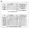
- FIG. 6 is an explanatory diagram illustrating an example of an address table of the battery voltage monitoring IC (pin addressing) according to the first embodiment.
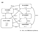
- FIG. 7 is an explanatory diagram illustrating a mutual Hamming distance of codes set in the mode setting terminal in the battery voltage monitoring device according to the third embodiment.
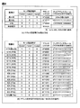
- FIG. 8 is an explanatory diagram illustrating an example of an address table of a battery voltage monitoring IC (auto addressing) according to the third embodiment.
- FIG. 9 is an explanatory diagram showing the operation of automatic address setting in auto addressing.
- FIG. 10 is a timing chart showing the operation of automatic address setting in auto addressing (bit shift).
- FIG. 11 is a timing chart showing the operation of automatic address setting in auto addressing (increment).
- FIG. 12 is a block diagram of a battery voltage monitoring device having interrupt signal communication configured in a daisy chain.
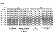
- FIG. 13 is an explanatory diagram showing the status register batch read operation in the test mode.
- FIG. 14 is a timing chart showing the status register batch read operation in the test mode.
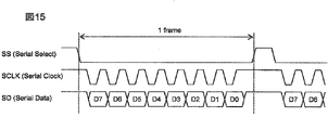
- FIG. 15 is a one-frame timing chart showing an example of the operation of daisy chain communication.
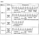
- FIG. 16 is an example of a frame format for each operation in various communication modes.
- the state of the arrangement setting terminal group for designating that it is connected to the first tap is a first symbol
- the state of the arrangement setting terminal group for designating that it is connected to the second tap is Two codes are used.
- the mode determination circuit cuts off the output from the communication signal terminal by the output switching circuit when the state of the arrangement setting terminal group is a Hamming distance of 1 with the first code or the second code.
- the MCU that functions as a system control device and a plurality of battery voltage monitoring ICs can be made with less wiring, reducing component costs, and providing a high-performance communication interface for each of the battery voltage monitoring ICs.
- it can be realized in consideration of fail-safe.
- the output switching circuit can switch whether the communication signal terminal is driven by a voltage source (12), a current source (11), or a high impedance.
- the mode determination circuit drives the communication signal terminal with the voltage source by the output switching circuit when the state of the arrangement setting terminal group coincides with the first code.
- the communication signal terminal is driven by a current source by the output switching circuit.
- the output switching circuit sets the communication signal terminal to high impedance.
- the circuit connected to the communication signal terminal is a voltage input type or a current input type.
- it is suitable for driving a current-driven boost level shifter when placed at the lowest potential end, and for driving a voltage input type insulating element (isolator) when placed at the highest potential end. Is preferred.
- a 1-bit error occurs in the internal IC address signal and the communication signal terminal is set to high impedance, there is no possibility of damaging the external circuit, and it becomes fail-safe.
- the arrangement setting terminal group is an address setting terminal (6), further includes an address register (30), and is set to the address setting terminal The address register is set based on
- the address of the battery voltage monitoring IC can be set from the outside of the IC by the voltage level (low fixed / high fixed, pull down / pull up, etc.) applied to the address setting terminal (6).
- the semiconductor device (battery voltage monitoring IC) according to Item 1 or 2, further comprising an address register (30) and a communication signal input terminal (5), wherein the communication signal terminal is a communication signal output terminal (4),
- An arrangement setting terminal group is a mode setting terminal (7), and sets the address register based on a state set in the mode setting terminal and a value input from the communication signal input terminal.
- the address of the battery voltage monitoring IC is determined by the voltage level (low fixed / high fixed, pull down / pull up, etc.) applied to the mode setting terminal (7) and the value stored in the address register (30) inside the IC.
- the mode setting terminal (7) is used to set one of the three types, ie, the highest potential end / lowest potential end / intermediate position thereof, and the remaining detailed address is set in the address register. It can be set by the value stored in (30). Whether it is placed at the highest potential end or the lowest potential end is greatly affected by failure, so protection is strengthened. When placed in the middle, the impact of failure that causes an error in the address is compared. Therefore, it is possible to take measures such as strengthening recovery rather than protection.
- the semiconductor device (battery voltage monitoring IC) further includes an arithmetic circuit (15), an output selection circuit (16), and a register communication control circuit (17).
- the output selection circuit performs an operation by the arithmetic circuit on the signal input from the communication signal input terminal and outputs the signal to the communication signal output terminal, or the signal input from the communication signal input terminal as it is. Whether to output to the communication signal output terminal can be selected.
- an internal register can be accessed by the register communication control circuit based on the register access command.
- the address register When an IC address setting command and an IC address value are input from the communication signal input terminal, the address register is set based on the IC address value, and the output selection circuit is connected to the IC input from the communication signal input terminal. For the address value, a signal that has been subjected to computation by the computation circuit is selected and output to the communication signal output terminal.
- the IC address can be set from the outside, and the number of terminals for specifying the IC address can be minimized.
- step S1 Next-stage IC address generation by increment>
- the signal input to the communication signal input terminal is a bit serial signal
- the signal output from the communication signal output terminal is a bit serial signal
- the arithmetic circuit is associated with the IC address setting command.
- the address value input in step S1 is incremented and output from the communication signal output terminal.
- IC address values are sequentially given to adjacent semiconductor devices (battery voltage monitoring ICs) (1_1 to 1_M) to increase code efficiency (represent many addresses with a small number of bits). Can do.
- the first IC address setting command automatically sets the IC address in the address register, and the second and subsequent IC address setting commands diagnose whether or not the initially set IC address is held. be able to.
- Item 1 further includes an interrupt output terminal (52), and the mode determination circuit detects that the arrangement setting terminal group has a Hamming distance of 1 from the first code or the second code. Sometimes, an interrupt signal is output from the interrupt output terminal.
- a chip address determination circuit (22) that outputs an IC selection signal (32) based on chip address frame data input from the communication signal input terminal, and register address frame data input from the communication signal input terminal.
- a register address determination circuit (24) that outputs a register selection signal (33) based on the status register and a status register that can be specified by the register selection signal.
- the bit data corresponding to the IC address stored in the address register of the register read data frame input from the communication signal input terminal is designated by the register selection signal.
- the status register information is replaced and updated, and the updated register read data frame is transmitted from the communication signal output terminal.
- the status information can be read from a plurality of semiconductor devices (battery voltage monitoring ICs) (1_1 to 1_M) collectively (simultaneously and in parallel).
- the chip address determination circuit outputs the IC selection signal based on a value of a bit position specified by an IC address stored in the address register in the chip address frame.
- one semiconductor device battery voltage monitoring IC (1_1 to 1_M) can be specified by 1 bit in the chip address frame, and 0 to M battery voltage monitoring ICs can be simultaneously and independently arranged in parallel. Can be specified.
- Item 10 or Item 11 further includes a mode setting terminal (7), and the status register can store an IC address error.
- the chip address frame has a predetermined value
- the IC address error Is stored in the status register.
- the first IC address setting command automatically sets the IC address in the address register
- the second and subsequent IC address setting commands diagnose whether or not the initially set IC address is held. be able to.
- the diagnosis result is stored in the status register as an IC address error, and can be read from a plurality of semiconductor devices (battery voltage monitoring ICs) (1_1 to 1_M) at once by a status register batch read command.
- a battery voltage monitoring device comprising: M voltage measurement units from the first voltage measurement unit (2_1) to the Mth voltage measurement unit (2_M) and the battery system control unit 3; Is done.
- the M voltage measurement units from the first voltage measurement unit (2_1) to the Mth voltage measurement unit (2_M) have a maximum potential end (93) close to the positive electrode to a minimum potential end (94) close to the negative electrode.
- M (M is an integer of 3 or more) unit cells are sequentially arranged from the lowest potential end to the highest potential end, and are identified by addresses from the first address to the Mth address based on the arrangement.
- the battery system control unit and the first voltage measurement unit to the Mth voltage measurement unit are connected in a daisy chain (8), and the battery system control unit is configured to communicate the first system by communication using the daisy chain.
- the Mth voltage measurement unit can be accessed from the voltage measurement unit.
- the state of the arrangement setting terminal group for designating that it is connected to the unit cell group at the highest potential end is a first code, and the unit for designating that it is connected to the unit cell group at the lowest potential end. Let the state of the arrangement setting terminal group be the second code.
- Each of the first voltage measurement unit to the Mth voltage measurement unit uses the daisy chain when the state of the arrangement setting terminal group is 1 and the Hamming distance from the first code or the second code is 1. Block the communication.
- the MCU acting as a system controller and multiple battery voltage monitoring ICs can be done with less wiring, reducing component costs, and providing a high-performance communication interface for each battery voltage monitoring IC.
- it can be realized in consideration of fail-safe.
- the first voltage measurement unit drives the second communication wiring with a current source (11) when the set state of the arrangement setting terminal group is equal to the second code, and sets the arrangement setting terminal group.
- the second communication wiring is set to high impedance.
- the M-th voltage measurement unit drives the signal potential conversion element with a voltage source (12) when the set state of the arrangement setting terminal group is equal to the first code, and sets the arrangement setting terminal group When the hamming distance from the first code is 1, the connection to the signal potential conversion element is set to high impedance.
- each of the first voltage measurement unit to the Mth voltage measurement unit further includes an address register (30), and the arrangement setting terminal group is an address setting terminal (6), which is set as the address setting terminal.
- the address register is set based on the state to be set.
- the address of the voltage measuring unit (2_1 to 2_M) can be set from the outside of the IC by the voltage level (low fixed / high fixed, pull down / pull up, etc.) applied to the address setting terminal (6). .
- each of the first voltage measurement unit to the Mth voltage measurement unit further includes an address register (30), and the arrangement setting terminal group is a mode setting terminal (7), which is set as the mode setting terminal.
- the address register is set on the basis of a state designated and a value designated by communication using the daisy chain.
- the address of the voltage measuring unit is set by the voltage level (low fixed / high fixed, pull down / pull up, etc.) applied to the mode setting terminal (7) and the value stored in the address register (30) inside the IC. can do.
- the mode setting terminal (7) is used to set one of the three types, ie, the highest potential end / lowest potential end / intermediate position thereof, and the remaining detailed address is set in the address register. It can be set by the value stored in (30). Whether it is placed at the highest potential end or the lowest potential end is greatly affected by failure, so protection is strengthened. When placed in the middle, the impact of failure that causes an error in the address is compared. Therefore, it is possible to take measures such as strengthening recovery rather than protection.
- the communication using the daisy chain is serial communication, and the battery system control unit can issue a command consisting of a plurality of bits.
- the command includes a chip address frame including M bits that can independently specify which one of the first voltage measurement unit to the Mth voltage measurement unit is to be accessed.
- the address setting command indicates a chip address frame indicating that none of the first to Mth voltage measuring units to be accessed and an address value to be set in the first voltage measuring unit. Includes data frames.
- the first voltage measurement unit When the first voltage measurement unit receives the address setting command, the first voltage measurement unit stores a value based on the value of the data frame in the address register. Further, the first voltage measuring unit includes a new address frame that includes the received address setting command and a new data frame that includes a value obtained by performing a predetermined calculation on the value of the data frame. Instead of the address setting command, the command is sent to the second voltage measurement unit via the second communication line.
- Each of the second voltage measurement unit to the M-1th voltage measurement unit receives the received address setting command, and receives new data based on the value obtained by performing the calculation on the received address frame and the value of the received data frame. It is replaced with a new address setting command including a frame, and is sent to the voltage measuring unit in the next stage.
- the IC address can be set from the outside, and the number of terminals for specifying the IC address can be minimized.
- IC address values are sequentially given to adjacent semiconductor devices (battery voltage monitoring ICs) (1_1 to 1_M) to increase code efficiency (represent many addresses with a small number of bits). Can do.
- the first IC address setting command automatically sets the IC address in the address register, and the second and subsequent IC address setting commands diagnose whether or not the initially set IC address is held. be able to.
- a mode switching circuit which has a normal operation mode and a sleep mode, and switches from the normal operation mode to the sleep mode; and a binary code indicating which of the M cell groups is connected to the cell group And a mode determination circuit (20) for controlling the mode switching circuit based on the state of the layout setting terminal group.
- the state of the arrangement setting terminal group for designating that it is connected to the first tap is a first symbol
- the state of the arrangement setting terminal group for designating that it is connected to the second tap is Two codes are used.
- the mode switching circuit When the mode determination circuit detects that the state of the arrangement setting terminal group is a Hamming distance of 1 with the first code or the second code, the mode switching circuit normally Transition from the operation mode to the sleep mode.
- the MCU acting as a system controller and multiple battery voltage monitoring ICs can be done with less wiring, reducing component costs, and providing a high-performance communication interface for each battery voltage monitoring IC.
- it can be realized in consideration of fail-safe.
- Item 8 is further provided with an interrupt output terminal (52), and when the comparison result between the IC address value stored in the address register and the newly set IC address value does not match, the interrupt output terminal Outputs an interrupt signal.
- Item 9 or Item 22 further includes an interrupt input terminal (51), and when the signal input from the interrupt input terminal is an interrupt signal, or when the interrupt signal is output by the semiconductor device itself, An interrupt signal is output from the interrupt output terminal.
- a battery voltage monitoring device comprising M voltage measurement units from a first voltage measurement unit (2_1) to an Mth voltage measurement unit (2_M), and a battery system control unit, configured as follows:
- the M voltage measurement units from the first voltage measurement unit (2_1) to the Mth voltage measurement unit (2_M) have a maximum potential end (93) close to the positive electrode to a minimum potential end (94) close to the negative electrode.
- M (M is an integer of 3 or more) unit cells are sequentially arranged from the lowest potential end to the highest potential end, and are identified by addresses from the first address to the Mth address based on the arrangement.
- the battery system control unit and the first voltage measurement unit to the Mth voltage measurement unit are connected in a daisy chain (8), and the battery system control unit is configured to communicate the first system by communication using the daisy chain.
- the Mth voltage measurement unit can be accessed from the voltage measurement unit.
- the first voltage measurement unit to the Mth voltage measurement unit hold the arrangement addresses set for each.
- the battery system control unit transmits a chip address frame, a register address frame, and a register read data frame not including valid data from the first voltage measurement unit to the Mth voltage measurement unit by communication using the daisy chain. And a register read data frame including the read data is received.
- Each of the first voltage measurement unit to the Mth voltage measurement unit transmits the received chip address frame and register address frame as they are.
- Each of the first voltage measurement unit to the M-th voltage measurement unit has the arrangement of the register read data frame when the arrangement address set to each of the first voltage measurement unit to the M-th voltage measurement unit matches the arrangement address specified by the chip address frame.
- the bit position data corresponding to the address is updated by replacing the status information of the status register (25) designated by the register address frame, and the updated register read data frame is sent to the daisy chain.
- the status information can be read from a plurality of voltage measuring units (2_1 to 2_M) collectively (simultaneously and in parallel).
- the chip address frame is configured to include M address designation bits that can independently designate the M-th voltage measurement unit from the first voltage measurement unit.
- one voltage measurement unit (2_1 to 2_M) can be designated by 1 bit, and 0 to M voltage measurement units can be independently designated in parallel. .
- each of the first voltage measurement unit to the Mth voltage measurement unit further includes a mode setting terminal (7) and an address register (31) for holding the arrangement address, and the status register includes Chip address error can be stored.
- the chip address frame has a predetermined value
- an IC address is set in the address register based on the value of the register address frame.
- the IC address set in the address register is compared with the IC address stored in the address register, and when the result does not match, the chip address error is stored in the status register.
- the first IC address setting command automatically sets the IC address in the address register
- the second and subsequent IC address setting commands diagnose whether or not the initially set IC address is held. be able to.
- the diagnosis result is stored in the status register as an IC address error, and can be read from a plurality of semiconductor devices (battery voltage monitoring ICs) (1_1 to 1_M) at once by a status register batch read command.
- each of the first voltage measurement unit to the Mth voltage measurement unit further includes an interrupt output terminal (52), and the state of the arrangement setting terminal group is the first code or the second code.
- an interrupt signal is output from the interrupt output terminal.
- each of the first voltage measurement unit to the Mth voltage measurement unit further includes an interrupt output terminal (52), and an IC address set in the address register and an IC address stored in the address register When the result does not match, an interrupt signal is output from the interrupt output terminal.
- each of the first voltage measurement unit to the Mth voltage measurement unit further includes an interrupt input terminal (51), and when the signal input from the interrupt input terminal is an interrupt signal, Alternatively, when an interrupt is generated by itself, an interrupt signal is output from the interrupt output terminal.
- FIG. 1 is a block diagram showing a configuration example of a battery voltage monitoring IC according to the first embodiment, and a battery voltage monitoring device connected in a daisy chain that makes a round-trip communication with a battery system control unit and a plurality of battery voltage monitoring ICs. .
- An assembled battery is configured by connecting a plurality of unit cells in series in multiple stages. This is divided into M (M is an integer greater than or equal to 3) unit cell groups composed of a plurality of unit cells, and M voltage measurement units 2 equipped with a battery voltage monitoring IC 1 are arranged for each unit cell group. Since the M cell groups are originally connected in series, the arranged M voltage measuring units 2 have different potentials in stages from the lowest potential end 94 to the highest potential end 93. Usually, the lowest potential end 94 is the negative electrode 92 of the assembled battery, and the highest potential end 93 is the positive electrode 91.
- the assembled battery is divided into N ⁇ M cell groups, one battery voltage monitoring device is arranged for the M cell groups, and the entire battery voltage monitoring device is configured by the N battery voltage monitoring devices. May be.
- the present invention can be applied to a higher voltage assembled battery or a large-scale assembled battery in which a plurality of assembled batteries are connected in parallel.
- the M voltage measuring units 2 from the first voltage measuring unit 2_1 to the M-th voltage measuring unit 2_M are assigned arrangement addresses from the first address to the M-th address based on the arranged positions. Identified.
- the position at which the battery is arranged is the tap position of the cells connected in series, and corresponds to the potential of the assembled battery.
- the first voltage measuring unit 2_1 to which the first address is applied is connected to the lowest potential end 94, and is connected to the tap of the higher potential sequentially after the second voltage measuring unit 2_2, and the Mth voltage to which the Mth address is applied.
- the measurement unit 2_M is connected to the highest potential end 93.
- FIG. 1 shows a daisy chain 8 that performs one-round communication as a connection example.
- the first voltage measurement unit 2_1 and the battery system control unit 3 are connected by the first communication wiring 8_1, and the Mth voltage measurement unit 2_M and the battery system control unit 3 are connected to the M + 1th communication wiring 8_M + 1 via the signal potential conversion element 9.
- the first voltage measuring unit 2_1 and the second voltage measuring unit 2_2 are connected by the second communication wiring 8_2, and the M-1th voltage measuring unit 2_M-1 and the Mth voltage measuring unit 2_M are connected by the Mth communication wiring.
- the signal potential conversion element 9 is an insulating element (isolator) that transmits communication data while being DC-insulated, and is, for example, a photocoupler, an inductive coupling insulating element, a capacitive coupling insulating element, or the like.
- the voltage measuring units 2 from the first voltage measuring unit 2_1 to the Mth voltage measuring unit 2_M hold the arrangement addresses set for each.
- the battery system control unit 3 can access the first voltage measurement unit 2_1 to the Mth voltage measurement unit 2_M through communication using the daisy chain 8.
- the arrangement address is an address attached to the IC and is called an IC address.
- Each of the M voltage measurement units 2 from the first voltage measurement unit 2_1 to the Mth voltage measurement unit 2_M designates which cell group of the M cell groups is connected by a binary code.
- Arrangement setting terminal groups (6_1 to 6_M, 7_1 to 7_M) are provided.
- the arrangement setting terminal groups (6_1 to 6_M, 7_1 to 7_M) are input with the first code when designating that they are connected to the single cell group at the highest potential end, and are connected to the single cell group at the lowest potential end.
- the second code is input.
- the arrangement setting terminal may be fixed to high or low in the voltage measuring unit 2, pulled up or pulled down, or a digital signal may be input by other methods.
- Each of the M voltage measurement units 2 from the first voltage measurement unit 2_1 to the Mth voltage measurement unit 2_M indicates that the state of the input arrangement setting terminal group (6_1 to 6_M, 7_1 to 7_M) is the first code or When the Hamming distance from the second code is 1, communication using the daisy chain 8 is blocked. For example, the output to the communication lines (8_1 to 8_M + 1) of the daisy chain 8 is set to high impedance.
- Each of the M voltage measurement units 2 from the first voltage measurement unit 2_1 to the Mth voltage measurement unit 2_M is connected in the daisy chain 8 depending on which cell group among the M cell groups. It is necessary to adapt the characteristics of the circuit that drives the communication lines (8_1 to 8_M + 1) of the daisy chain 8 because the circuit to be connected is different.
- the first voltage measurement unit 2_1 is normally input from the battery system control unit 3 via the first communication line 8_1, which is at the same potential level, and the second voltage measurement unit 2_2 which is one step higher in potential level is connected to the second communication line. It will be driven via 8_2.
- the Mth voltage measurement unit is input from the M-1 voltage measurement unit 2_M-1 that is one level lower in potential level via the Mth communication line 8_M, and drives the signal potential conversion element 9.
- the presence or absence of the level shifter and the circuit system differ depending on the potential level, and the characteristics of the circuit that drives the communication lines (8_1 to 8_M + 1) of the daisy chain 8 must be adapted accordingly.
- Arrangement addresses from the first address to the Mth address are set in the arrangement setting terminal groups (6_1 to 6_M, 7_1 to 7_M), and based on this, which cell group is connected to among the M cell groups. Therefore, the characteristics of the circuit that drives the communication lines (8_1 to 8_M + 1) of the daisy chain 8 can be adapted accordingly. If the arrangement address is correct, the communication circuits constituting the daisy chain function correctly. However, when the state of the arrangement setting terminal groups (6_1 to 6_M, 7_1 to 7_M) is not a correct code due to a failure or the like, the communication circuit does not function correctly. Therefore, the concept of fail-safe is adopted.
- a portion where the influence of an address error due to a failure or the like is serious is mainly protected.
- failures at the highest potential end and the lowest potential end are more serious.
- the battery voltage measuring unit 2 connected to the intermediate potential is connected only by the adjacent battery voltage measuring unit 2 in a daisy chain, so the potential difference is not large, but it is arranged at the highest potential end and the lowest potential end. This is because the potential difference between the battery voltage measuring unit 2 and the connection destination is large, and in some cases, the potential difference between the highest potential end and the lowest potential end may be reached.
- Battery voltage monitoring ICs 1_1 to 1_M are mounted on each of the M voltage measuring units 2 from the first voltage measuring unit 2_1 to the Mth voltage measuring unit 2_M, and arrangement setting terminal groups (6_1 to 6_M, 7_1 to 7_M) are provided. The case of the terminal will be described in more detail.
- the communication signal input terminal 5_1 of the first voltage measurement unit 2_1 at the lowest potential end is driven by the MCU that works as the battery system control unit 3, and therefore generally has a voltage input.
- the communication signal output terminal 4_1 is connected via a level shifter. Since it is connected to the communication signal input terminal 5_2 of the second voltage measurement unit 2_2 on the one-stage high potential side, it is preferable to use a current output.
- the voltage measurement unit 2 in the second and subsequent stages is suitable for voltage input and current output because both input and output are connected to the level shifter.
- the communication signal input terminal 5_M of the Mth voltage measuring unit 2_M at the highest potential end is a voltage input because it is connected to the output of the level shifter.
- the communication signal output terminal 4_M is appropriately optimized according to the folded communication circuit system. For example, when circulating to the MCU 3 through an insulating element (isolator) 9 such as a photocoupler, the insulating element 9 is driven, so that a voltage output is often suitable.
- an insulating element (isolator) 9 such as a photocoupler
- the level shifter it is assumed that a signal that is current-output on the low potential side is converted into a voltage by a resistor on the high potential side.
- a step-down level shifter can also be realized by a similar circuit.
- the first voltage measurement unit 2_1 drives the second communication wiring 8_2 with a current source and sets the arrangement setting terminal group.
- the second communication wiring 8_2 is set to high impedance.
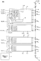
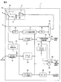
- FIG. 3 is a block diagram illustrating a more detailed configuration example of the battery voltage monitoring IC (pin addressing) according to the first embodiment.
- the battery voltage monitoring IC 1 includes a communication signal terminal 4, an address setting terminal 6 as the arrangement setting terminal, an output switching circuit 10 capable of switching whether to output or block a signal from the communication signal terminal, and an address setting terminal And a mode determination circuit 20 that controls the output switching circuit 10 based on the six states.
- the mode determination circuit 20 shuts off the output from the communication signal terminal 4 by the output switching circuit 10 when the address setting terminal 6 is in the Hamming distance of 1 with the first code or the second code.
- the output switching circuit 10 can switch whether the communication signal terminal 4 is driven by the voltage source 12, the current source 11, or the high impedance.
- the address determination circuit 20 controls the communication signal terminal 4 as follows.
- the communication signal terminal 4 is driven by the voltage source 12 by the output switching circuit 10.
- the output signal switching circuit 10 drives the communication signal terminal 4 with the current source 11.
- the output switching circuit 10 sets the communication signal terminal 4 to high impedance.
- the circuit connected to the communication signal terminal is a voltage input type or a current input type.
- it is suitable for driving a current-driven boost level shifter when placed at the lowest potential end, and for driving a voltage input type insulating element (isolator) when placed at the highest potential end. Is preferred.
- a 1-bit error occurs in the state of the address setting terminal 6, by detecting this and making the communication signal terminal high impedance, there is no possibility of damaging the external circuit, resulting in fail safe.
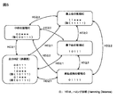
- FIG. 5 is an explanatory diagram showing the mutual Hamming distance of the arrangement address of the battery voltage monitoring IC (the arrangement address of the battery voltage monitoring module) set in the address setting terminal 6 in the battery voltage monitoring apparatus according to the first embodiment.
- This numerical example is a setting example of an arrangement address in a battery voltage monitoring system that can be connected to a cell group in which eight cells are connected in series.
- B'11 *** except b'11111 is given as an arrangement address to the highest-level monitoring IC 1 arranged at the highest potential end.
- “b ′” represents a binary number
- “b′11111” represents a numerical value in which all bits are 1 in a 5-digit binary number.
- B'10111 is given to the lowest-order monitoring IC 1 arranged at the lowest potential end.
- the Hamming distance is always 2 or more with respect to the arrangement address b'10111 of the lowest-order monitoring IC1.
- the arrangement address of the middle monitoring IC between the highest level and the lowest level may be b'00 *** except b'00111.
- the Hamming distance between the uppermost monitoring IC and the lowermost monitoring IC and the arrangement address of the middle monitoring IC is 2 or more.
- the arrangement address b'01111 may be given.
- any of the highest, lowest, and middle monitoring ICs can have two or more Hamming distances.
- the arrangement address whose Hamming distance is 1 from the arrangement addresses of the highest-order, lowest-order, middle-order monitoring ICs, and the single-use monitoring IC is an arrangement address whose output should be controlled to HiZ.
- there may be a plurality of middle-level monitoring ICs, and the arrangement addresses to be set for them are characterized in that the Hamming distance 1 is allowed.
- FIG. 5 shows an example in which eight monitoring ICs 1 can be identified.
- the present invention can be extended to a method of assigning arrangement addresses that can identify the number of monitoring ICs 1 or less.
- the number of bits of the arrangement address may be increased by 1, that is, the number of the address setting terminals 6 may be increased by one.
- the address allocation method of the present embodiment can reduce the number of bits for expressing the arrangement address, and can reduce the number of address setting terminals 6 to be provided in the monitoring IC.
- the battery voltage monitoring IC 1 can further set the address register 30 based on the state set in the address setting terminal 6.
- a value inputted from the address setting terminal 6 is taken into the address reading circuit 18 immediately after power-on, for example, is converted into an IC address value through the address table 19, and then stored in the address register 30.
- the address register 30 can be set from the outside of the IC by the voltage level applied to the address setting terminal 6.
- a desired address can be set by fixing the address setting terminal 6 low or high, or pulling down or pulling up.
- FIG. 6 is an explanatory diagram illustrating an example of an address table of the battery voltage monitoring IC (pin addressing) according to the first embodiment.
- the relationship between the state of the address setting terminal 6 and the value stored in the address register is associated.
- (A) is a general setting method
- the chip address frame is a display example in a communication frame for designating a chip address to be accessed in daisy chain communication. The operation of daisy chain communication and the format of the communication frame will be described later.
- the address is stored in the address register.
- the highest address can be b'11000
- the lowest address can be b'11111
- the middle address can be b'11 ***.
- the battery voltage monitoring IC 1 includes various registers not shown. There are a control register for controlling the battery voltage monitoring IC 1, a data register for holding data, a status register for holding the state of the battery voltage monitoring IC 1 and the state of the unit cell to be measured. These registers are provided with register addresses, and the battery system control unit 3 can specify a chip address and a register address to access a desired register.
- FIG. 15 is a timing chart of one frame showing an example of the operation of daisy chain communication
- FIG. 16 is an example of a frame format for each operation in various communication modes.
- Daisy chain communication is realized by a serial select signal SS, a serial clock signal SCLK, and a serial data signal SD.
- Each bit can be composed of at least three signal lines.
- the signal line may be differentiated using twice as many signal lines, and the data may be partially parallelized.
- FIG. 15 shows an example in which one frame is composed of 8 bits. The number of bits can be arbitrarily determined.
- the battery system control unit 3 is a host, and the battery voltage monitoring ICs (1_1 to 1_M) are ICs.
- the first frame and the second frame constitute a chip address frame and designate an IC address.
- a register address is designated in the third frame, and a write command is also designated.
- Write data is designated in the fourth frame.
- a CRC (Cyclic Redundancy Check) code for error detection with respect to the commands of the first to fourth frames is transmitted. From the seventh frame to the tenth frame, a response signal can be transmitted (returned) from each accessed IC.
- Register writing is generally an operation that is completed in one direction from the host to the IC, and it is not necessary to return a response signal.
- the chip address frame is configured to include the same number of bits as the number of connected ICs.
- up to 16 ICs can be specified.
- up to 16 ICs can be designated independently. The same value can be simultaneously written in parallel to a maximum of 16 ICs.
- each IC can be sequentially designated and an independent value can be written.
- the first frame and the second frame constitute a chip address frame and designate an IC address.
- the register address is specified in the third frame, and the read command is also specified.
- CRC codes for error detection with respect to the commands of the first to fourth frames are transmitted.
- read data having the number of frames corresponding to the data size specified in the fourth frame is transmitted (returned) from the accessed IC with the CRC code for the read data added.
- FIG. 16 shows a case where the chip address frame is 2 frames, the register address and the command frame for designating read / write are 1 frame, and the read data and CRC code are each 2 bytes.
- the format including the number of frames (number of frames) can be arbitrarily set.
- All frames in the daisy chain communication are input from the communication signal input terminal 5 and are added as they are or a response frame or the like is added, or some data of the received frame is rewritten and sent to the battery voltage monitoring IC 1 at the subsequent stage. Therefore, it is output from the communication signal output terminal 4.
- the circuits related to the serial select signal SS and the serial clock signal SCLK are not shown, and the serial data signal SD is input from the communication signal input terminal 5.
- the serial data signal SD input from the communication signal input terminal 5 is serial-parallel converted and input in parallel to the register communication control circuit 17, the chip address frame extraction circuit 21, and the register address frame extraction circuit 23.
- the chip address frame extraction circuit 21 detects that the input serial data signal SD is the first frame and the second frame in the frame format, it is transferred to the IC selection / non-selection determination circuit 22 and is sent to the address register
- the IC address is compared with the IC address stored in 30, and if they match, an IC selection signal 32 is output.
- the register address frame extraction circuit 23 that the input serial data signal SD is the third frame and the fourth frame in the frame format, it is transferred to the register address determination circuit 24 constituted by a decoder, A register selection signal 33 is output.
- the register address determination circuit 24 also determines whether it is a write command or a read command. When it is determined by the IC selection signal 32 that its own IC is to be accessed, a register (not shown in FIG. 3) designated by the register selection signal 33 in accordance with the determined read command / write command And a response frame is formed by the register communication control circuit 17 based on the access result. The register communication control circuit 17 also calculates the CRC of the response frame and adds the CRC frame. The configured response frame is output from the communication signal output terminal 4 via the parallel-serial converter 54, the output selection circuit 16, and the output switching circuit 10.
- the block diagram of FIG. 3 is described according to the frame configuration shown in FIG. 16, and is merely an example.
- the frame format may be appropriately determined according to the number of ICs to be communicated, the number of registers per IC, and the like, such as how many bits constitute one frame and the chip address frame.
- FIG. 2 is a block diagram illustrating a configuration example of a battery voltage monitoring device according to the second embodiment and a battery voltage monitoring device connected in a daisy chain that performs loopback communication with the battery system control unit and a plurality of battery voltage monitoring ICs. .
- the daisy chain 8 that performs one-round communication is shown as an example of connection, but in the second embodiment, the daisy chain 8 that performs loopback communication is illustrated.
- the battery system control unit 3 is the same in that the M voltage measurement units 2 from the first voltage measurement unit 2_1 to the Mth voltage measurement unit 2_M are connected by the daisy chain 8, but the battery system control unit 3 To the M-th voltage measuring unit 2_M, which is the highest potential end, and an upstream communication path (8_U_1 to 8_U_M) and a downstream communication path (8_D_M to 8_D_1).
- Each of the battery voltage monitoring ICs 1_1 to 1_M includes an output switching circuit 10_U for uplink communication, a communication signal input terminal 5_U, and a communication signal output terminal 4_U, and further includes an output switching circuit 10_D for downlink communication and a communication signal input. A terminal 5_D and a communication signal output terminal 4_D.
- the output switching circuit 10_U for uplink communication and the output switching circuit 10_D for downlink communication are controlled by the mode determination circuit 20 so as to be suitable for each uplink and downlink.
- the battery voltage monitoring IC 1 designated as the access target in the register read command can respond by itself without waiting for a reply from the subsequent stage. Further, the signal potential conversion element 9 can be dispensed with.
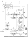
- FIG. 4 is a block diagram illustrating a configuration example of a battery voltage monitoring IC (auto addressing) according to the third embodiment.
- the battery voltage monitoring IC pin addressing
- all arrangement addresses are set by the address setting terminal 6.
- the mode setting terminal 7 sets only information about whether the IC is arranged at the highest potential end, the lowest potential end, or the middle thereof.
- FIG. 7 is an explanatory diagram showing the mutual Hamming distance of the codes set in the mode setting terminal 7 in the battery voltage monitoring device according to the third embodiment.
- the uppermost battery voltage monitoring IC 1 arranged at the highest potential end 93 is given b′110 as an arrangement address
- the lowermost battery voltage monitoring IC1 arranged at the lowest potential end 94 is given b′101.
- the arrangement address of the middle battery voltage monitoring IC between the highest and lowest is b'000
- the Hamming distance of the arrangement address in both the highest battery voltage monitoring IC and the lowest battery voltage monitoring IC Becomes 2 or more. Further, when the battery voltage monitoring IC is used alone, the arrangement address b'011 may be given.
- the output is set to high impedance and the communication path is Block (non-communication).
- the arrangement address whose Hamming distance is 1 from the arrangement addresses of the highest, lowest, and middle battery voltage monitoring ICs and the single-use battery voltage monitoring IC is an arrangement address whose output should be controlled to HiZ.
- FIG. 5 shows an example in which eight battery voltage monitoring ICs 1 can be identified, and the number of address setting terminals 6 at that time is 5 pins. Each time the number of battery voltage monitoring ICs 1 is doubled, the number of address setting terminals 6 is increased by one pin.
- the mode setting terminal 7 has 3 pins regardless of the number of battery voltage monitoring ICs.
- the chip address stored in the address register is calculated based on only the setting information of the address setting terminal 6 and set in the address register 30, but the mode setting terminal 7 Since there are only three regardless of the number of battery voltage monitoring ICs, it is not possible to set a unique address for all the battery voltage monitoring ICs with this information alone. Therefore, the IC address to be stored in the address register 30 is given by communication using a daisy chain in addition to the setting information of the mode setting terminal 7.
- the first frame and the second frame constitute a chip address frame as in the normal mode.
- the normal mode at least one IC is an access target, whereas the first frame and the second frame in the addressing mode are configured by data that neither IC is designated as an access target. Since it is self-evident that the address registers of all ICs are to be accessed in the addressing mode, a chip address frame composed of data that is not specified as an access target in any IC that is not specified in the normal mode. Thus, it can be detected that the mode is the addressing mode.
- the IC address value to be set in the first-stage battery voltage monitoring IC 1 is given to the third and fourth frames following the first and second frames indicating the addressing mode.
- the battery voltage monitoring IC 1 at the first stage sets the address register 30 based on the value, performs a predetermined calculation, and sends it to the battery voltage monitoring IC at the next stage.
- the values of the third frame and the fourth frame extracted by the register address frame extraction circuit 23 are written to the address diagnosis register 26 via the address table 19 and then transferred to the address register 30 via the transfer circuit 27. Is done.
- the address register 30 is set based on the values specified in the third frame and the fourth frame of daisy chain communication.
- the values of the third frame and the fourth frame are subjected to predetermined arithmetic processing by the arithmetic circuit 15 and output from the communication signal output terminal 4 via the output selection circuit 16 and the output switching circuit 10. It is transferred to the monitoring IC.
- the address register 30 is set by the same operation in the monitoring IC at the next stage.
- the IC address to be set can be a value different from that of the first stage. Furthermore, even if the transfer is performed in multiple stages and the address is set, a unique IC address can be set for each of all the monitoring ICs by appropriately selecting the type of calculation.
- FIG. 8 is an explanatory diagram illustrating an example of an address table of the battery voltage monitoring IC (auto addressing) according to the third embodiment.
- the value set in the address register can be a unique value from the lowest b'11111 to the highest b'10000.
- FIG. 9 is an explanatory diagram showing the operation of automatic address setting in auto addressing.
- 16 schematically shows an operation in which the chip address frame by the first frame and the second frame shown in FIG. 16 and the register address frame by the third frame and the fourth frame are sequentially transferred from the eight battery voltage monitoring ICs 1_1 to 1_8. It is a representation.
- the chip address frame indicates one battery voltage monitoring IC with 1 bit, and indicates that it is an access target when b'0. Since the chip address frame is composed of a total of 16 bits for the first frame and the second frame, it can be used in a daisy chain in which a maximum of 16 ICs are connected. In FIG. A daisy chain of ICs is shown.
- the battery system control unit 3 sends b′01111111 and 11111111 to the register address frame to the first-stage battery voltage monitoring IC 1_1.
- the battery voltage monitoring IC 1_1 at the first stage refers to the address table shown in FIG. 8 and sets the IC address b′11111 corresponding to b′01111111 and 11111111 in the address register 30 in the register address frame.
- the address frame is shifted by 1 bit, changed to b′10111111 and 11111111, and sent to the battery voltage monitoring IC1_2 at the next stage.
- the battery voltage monitoring ICs 1_2 to 1_7 set the value of the address register based on the received register address frame, and send out the register address frame sequentially shifted by 1 bit to the next stage.
- the IC address can be set from the outside, and the number of terminals for specifying the IC address can be minimized.
- FIG. 10 is a timing chart showing an automatic address setting operation in auto addressing (bit shift).
- the operation for the register address frame is bit-shifted.
- the bit shift may be performed in synchronization with SCLK as shown in the timing chart of FIG.
- FIG. 11 is a timing chart showing the operation of automatic address setting in auto addressing (increment). This is an example in which the calculation for the register address frame by the calculation circuit 15 is incremented. In order to increment the register address frame, the register address frame is once converted to a parallel value, 1 is added, and then the serial value is returned again to the next stage. Since serial-parallel conversion needs to be executed after all the data is ready, a delay of one frame cycle occurs. In FIG. 11, the illustration of SCLK is omitted, and the change for each frame cycle indicated by SS is shown. While it takes time to complete the setting of the address registers 30 of all the monitoring ICs 1_1 to 1_8, the register address frame is sequentially incremented. Therefore, it is possible to set addresses for many monitoring ICs with a small number of bits. it can. For example, an address can be set for 256 monitoring ICs even in an 8-bit register address frame.
- IC address values are sequentially given to adjacent semiconductor devices (battery voltage monitoring ICs) (1_1 to 1_M) to increase code efficiency (represent many addresses with a small number of bits). Can do.
- the values of the third frame and the fourth frame extracted by the register address frame extraction circuit 23 are sent to the address diagnosis register via the address table 19. 26 is transferred to the address register 30 through the transfer circuit 27.
- the address register 30 is set based on the values specified in the third frame and the fourth frame of daisy chain communication.
- the IC address to be set based on the register address frame is temporarily stored in the address diagnosis register 26.
- the IC address set in the address register 30 is compared with the IC address to be set by the comparison circuit 28. The result is output as an address comparison match signal (diagnosis) 34.
- the auto addressing command for setting the same IC address as the initial setting, it can be used for diagnosis whether or not the same IC address as the IC address to be set is set. Since the commands are the same, a mismatch result is output at the time of initial setting, but the battery system control unit 3 that issues the command may ignore the result of mismatch when it is the initial setting. The same applies to resetting or changing settings. If a mismatch result is expected when a match result is expected, it can be diagnosed that some failure has occurred in the address register. Match or mismatch results can be stored in a status register. The battery system control unit 3 may read and confirm the contents of the status register after issuing the auto addressing command.
- an interrupt signal may be generated. Since the interrupt signal is output from each monitoring IC, it may be connected to the battery system control unit 3 at 1: 1, or may be connected via a common bus. However, in the battery voltage monitoring system, the operating potentials of the respective monitoring ICs are different, so that a large number of insulating elements (isolators) are required regardless of whether they are connected 1: 1 or via a common bus. . Therefore, it is more preferable to configure the communication signal line 8 with a daisy chain.
- FIG. 12 is a block diagram of a battery voltage monitoring device having interrupt signal communication configured in a daisy chain.
- Each of the battery voltage monitoring ICs 1_1 to 1_8 includes an interrupt output terminal 52 and an interrupt input terminal 51, and is connected in a daisy chain.
- the output switching circuit 10 controlled by the mode determination circuit 20 is connected to the interrupt output terminal 52, and in the event of a failure, communication is cut off by switching to high impedance. You can also. A relatively minor failure can be notified to the battery system control unit 3 by an interruption and recovered, but a serious failure can be quickly shut down to avoid a serious effect.
- FIG. 12 shows an example of a round-trip communication.
- an insulating element (isolator) 9 may be required in the path from the highest battery voltage monitoring IC 1_8 to the battery system control unit 3, but the illustration is omitted.
- a daisy chain of loopback communication similar to that shown in FIG. 2 can be configured. In this case, however, the interrupt output terminal 52 and the interrupt input terminal 51 need to be provided with two systems, upstream and downstream. In order to transmit the interrupt signal, the transmission subject is the battery voltage monitoring IC 1 in which the interrupt has occurred.
- the battery voltage monitoring IC 1 that has generated the interrupt can send an interrupt signal to the battery system control unit 3 by a method such as issuing a write command that designates the battery system control unit 3 using a chip address frame.
- a transmission method and a method for arbitrating contention when interrupts are simultaneously generated from a plurality of battery voltage monitoring ICs can be realized following a known communication method using daisy chain communication.
- FIG. 13 is an explanatory diagram showing an operation of status register batch reading in the test mode
- FIG. 14 is a timing chart showing an operation of status register batch reading in the test mode.
- the battery voltage monitoring IC 1 is provided with various status registers. For example, a status indicating an abnormality of a cell to be monitored, a CRC error status when an error is detected by calculating a CRC of a command received by daisy chain communication, and a diagnosis of the address register shown in the fourth embodiment is performed. Error status indicating the error in the case.
- the occurrence of the error can be notified to the battery system control unit 3 by interruption, but there are many cases where the cause of the error cannot be notified. This is because the notification of an interrupt gives priority to quickness, and therefore the communication protocol is simplified and the amount of information that can be transmitted is often limited.
- the battery system control unit 3 that has been notified of the occurrence of the abnormality by an interruption reads the information in the status register in order to investigate the cause of the error.
- the status register batch reading in the fifth embodiment reads the contents of the status register from all the battery voltage monitoring ICs connected in a daisy chain by issuing one command.
- the frame format can be configured, for example, as shown in the test mode column of FIG.
- the chip address frame is composed of the first frame and the second frame, and the read command is designated in the third frame and the address of the status register to be read is designated.
- the read command is configured so that only one monitoring IC can be specified for the chip address frame.
- all monitoring ICs are simultaneously designated as access targets even by a read command.
- the read data is output to a read data frame composed of the seventh frame and the eighth frame.
- FIG. 13 shows the status register batch read operation in a daisy chain composed of eight battery voltage monitoring ICs.
- FIG. 13 shows read data frames output from the battery voltage monitoring ICs 1_1 to 1_8.
- the battery voltage monitoring IC 1_1 writes the status register information a in the first bit and sends it to the battery voltage monitoring IC 1_2 at the next stage.
- the battery voltage monitoring IC 1_2 keeps the first bit of the received read data frame, writes the information b of its own status register in the second bit, and sends it to the battery voltage monitoring IC 1_3 in the next stage. Thereafter, in the received read data frame, information of its own status register is written in a bit position determined based on its own IC address, and sent to the battery voltage monitoring IC of the next stage.
- the status information collected via all eight battery voltage monitoring ICs 1_1 to 1_8 is collectively received by the battery system control unit 3.
- FIG. 14 is a timing chart of this operation.
- new status information is sequentially added in synchronization with SCLK.
- SCLK clockwise synchronization
- the status information can be read from a plurality of semiconductor devices (battery voltage monitoring ICs) (1_1 to 1_M) collectively (simultaneously and in parallel).
- the present invention can be effectively applied to a voltage monitoring device for a power source in which large-capacity capacitors such as ion capacitors are connected in series in multiple stages.
- the present invention relates to a battery voltage monitoring device and a semiconductor device used therefor, and in particular, can be widely applied to fail-safe design in communication of a battery voltage monitoring IC.
Landscapes
- Engineering & Computer Science (AREA)
- Power Engineering (AREA)
- Life Sciences & Earth Sciences (AREA)
- Mechanical Engineering (AREA)
- Transportation (AREA)
- Sustainable Energy (AREA)
- Sustainable Development (AREA)
- Chemical Kinetics & Catalysis (AREA)
- General Chemical & Material Sciences (AREA)
- Electrochemistry (AREA)
- Chemical & Material Sciences (AREA)
- Manufacturing & Machinery (AREA)
- Computer Networks & Wireless Communication (AREA)
- Physics & Mathematics (AREA)
- General Physics & Mathematics (AREA)
- Charge And Discharge Circuits For Batteries Or The Like (AREA)
- Secondary Cells (AREA)
- Battery Mounting, Suspending (AREA)
Abstract
Description
50)、そのコマンドの種類の判定を行なう(ステップ51)。この判定で、アドレス再設定コマンドと判定した場合には、スレーブ側制御手段(14)が持つ乱数発生部(15)(ここでは電池電圧検出データをシードとする乱数発生プログラム)を用いて1~N以下(Nは予め定めた上限値でここでは255とする)の乱数を発生させ、その乱数を仮の自己アドレスとする(ステップ52)。次いで、返信データの準備を行ない(ステップ53)、その仮アドレスを待ち時間としてカウントし、採用した乱数による返信待ち時間の調整処理を行ない(ステップ54)、その仮アドレスを返信処理し、マスター側制御手段(23)に送信する(ステップ55)。スレーブ側制御手段(14)から仮アドレスの送信を受けたマスター側制御手段(23)は、仮アドレスの受信処理を行ない(ステップ41)、有効受信データ件数が仮アドレスの種類数と同じか否かを判定する(ステップ42)。このステップ42の判定では、有効受信データ件数と仮アドレスの種類数が同じでない場合にはステップ40に戻ってアドレス再設定コマンドの発行を行ない、有効受信データ件数と仮アドレスの種類数が同じになるまで繰り返す。マスター側制御手段(23)側では、全てのスレーブ側制御手段(14)が異なる仮アドレスであるとすれば、有効受信データ件数と仮アドレスの種類数が最終的に同じになるはずであるからである。ステップ42において、有効受信データ件数と仮アドレスの種類数が同じになった場合には、マスター側制御手段(23)は仮アドレスに重複があるか判定する(ステップ43)。この判定で、仮アドレスに重複がある場合には、ステップ40に戻ってアドレス再設定コマンドの発行を行ない、仮アドレスの重複がなくなるまで繰り返す。そして、仮アドレスの重複がなくなった場合には、スレーブ側制御手段(14)の全てに異なるアドレスデータが配分されるものとして、マスター側制御手段(23)はアドレス確定コマンドの発行を行ない、全てのスレーブ側制御手段(14)に送信する。スレーブ側制御手段(14)では、このアドレス確定コマンドの送信を受けて、コマンド受信処理をし(ステップ50)、そのコマンドの種類の判定を行なう(ステップ51)。この判定で、コマンドがアドレス確定コマンドであると判定した場合には、その仮アドレスをマスター側制御手段(23)の本当の自己アドレスとして記憶部16に記憶し(ステップ56)、ステップ53からステップ55の処理を行なう。このようにして自動的に複数の電池監視装置2のアドレスを確定させることができる。このように、乱数発生部(15)により仮アドレスを発生してこれを自己アドレスに確定するように処理動作させたので、簡単に各電池監視装置(2)に自己アドレスを設定することができる。
先ず、本願において開示される発明の代表的な実施の形態について概要を説明する。代表的な実施の形態についての概要説明で括弧を付して参照する図面中の参照符号はそれが付された構成要素の概念に含まれるものを例示するに過ぎない。
正極(91)と負極(92)の間に多段に直列接続されることにより組電池を構成する複数の単電池のうち、前記正極に近い第1タップ(93)から前記負極に近い第2タップ(94)までの、M個(Mは3以上の整数)の単電池グループ毎に配置され、前記グループに属する単電池を監視するための半導体装置(電池電圧監視IC)(1_1~1_M)であって、以下のように構成される。
項1において、前記出力切替回路は、前記通信信号端子を電圧源(12)で駆動するか、電流源(11)で駆動するか、ハイインピーダンスにするかを切り替え可能である。
項1または項2において、半導体装置(電池電圧監視IC)は、前記配置設定端子群はアドレス設定端子(6)であり、アドレスレジスタ(30)をさらに備え、前記アドレス設定端子に設定される状態に基づいて前記アドレスレジスタを設定する。
項1または項2において、半導体装置(電池電圧監視IC)は、前記通信信号端子を通信信号出力端子(4)とし、アドレスレジスタ(30)と通信信号入力端子(5)とをさらに備え、前記配置設定端子群はモード設定端子(7)であり、前記モード設定端子に設定される状態と前記通信信号入力端子から入力される値に基づいて、前記アドレスレジスタを設定する。
項4において、半導体装置(電池電圧監視IC)は、演算回路(15)と出力選択回路(16)とレジスタ通信制御回路(17)をさらに備える。
項5において、前記通信信号入力端子に入力される信号はビットシリアル信号であり、前記通信信号出力端子から出力される信号はビットシリアル信号であり、前記演算回路による演算がビットシフトである。
項5において、前記通信信号入力端子に入力される信号はビットシリアル信号であり、前記通信信号出力端子から出力される信号はビットシリアル信号であり、前記演算回路は、前記ICアドレス設定コマンドに伴って入力された前記アドレス値をインクリメントして前記通信信号出力端子から出力する。
項5において、前記通信信号入力端子からICアドレス設定コマンドとICアドレス値が入力されたとき、前記ICアドレス値に基づいて前記アドレスレジスタに設定される値と、前記アドレスレジスタに格納されている値との比較を行う。
項1において、割り込み出力端子(52)をさらに備え、前記モード判定回路により、前記配置設定端子群の状態が前記第1符号または前記第2符号とのハミング距離が1であることが検出されたときに、前記割り込み出力端子から割り込み信号を出力する。
正極(91)と負極(92)の間に多段に直列接続されることにより組電池を構成する複数の単電池のうち、複数の単電池グループ毎に配置され、ICアドレスが与えられ、前記グループに属する単電池を監視するための半導体装置(電池電圧監視IC)(1_1~1_M)であって、以下のように構成される。
項10において、前記チップアドレス判定回路は、前記チップアドレスフレームにおける前記アドレスレジスタに格納されているICアドレスによって特定されるビット位置の値に基づいて、前記IC選択信号を出力する。
項10または項11において、モード設定端子(7)をさらに備え、前記ステータスレジスタはICアドレスエラーを格納可能である。前記チップアドレスフレームが所定の値のときに、前記レジスタアドレスフレームの値に基づいて前記アドレスレジスタに設定される値と、前記アドレスレジスタに格納されている値とが異なるときに、前記ICアドレスエラーを前記ステータスレジスタに格納する。
正極(91)と負極(92)の間に多段に直列接続されることにより組電池を構成する複数の単電池のうち、M個(Mは3以上の整数)の単電池グループ毎に配置される第1電圧測定部(2_1)から第M電圧測定部(2_M)までのM個の電圧測定部と、電池システム制御部3とを備える、電池電圧監視装置であって、以下のように構成される。
項13において、前記第1電圧測定部と前記電池システム制御部とが第1通信配線(8_1)で接続され、前記第M電圧測定部と前記電池システム制御部とが信号電位変換素子(9)を介して第M+1通信配線(8_M+1)で接続される。また、前記第1電圧測定部と第2電圧測定部とが第2通信配線(8_2)で接続され、第M-1電圧測定部と前記第M電圧測定部が第M通信配線(8_M)で接続される。
前記第1電圧測定部は、設定された前記配置設定端子群の状態が前記第2符号と等しいときには、前記第2通信配線を電流源(11)で駆動し、設定された前記配置設定端子群の状態が前記第2符号とのハミング距離が1であるときには、前記第2通信配線をハイインピーダンスにする。
前記第M電圧測定部は、設定された前記配置設定端子群の状態が前記第1符号と等しいときには、前記信号電位変換素子を電圧源(12)で駆動し、設定された前記配置設定端子群の状態が前記第1符号とのハミング距離が1であるときには、前記信号電位変換素子との接続をハイインピーダンスにする。
項13において、前記第1電圧測定部から前記第M電圧測定部は、それぞれアドレスレジスタ(30)をさらに備え、前記配置設定端子群はアドレス設定端子(6)であり、前記アドレス設定端子に設定される状態に基づいて前記アドレスレジスタを設定する。
項13において、前記第1電圧測定部から前記第M電圧測定部は、それぞれアドレスレジスタ(30)をさらに備え、前記配置設定端子群はモード設定端子(7)であり、前記モード設定端子に設定される状態と前記デイジーチェーンを使った通信によって指定される値に基づいて、前記アドレスレジスタを設定する。
項16において、前記デイジーチェーンを使った前記通信はシリアル通信であり、前記電池システム制御部は、複数ビットからなるコマンドを発行可能である。
項17において、前記演算が、受信したデータフレームの値のビットシフトである。
項17において、前記演算が、受信したデータフレームの値のインクリメントである。
項17において、前記第1電圧測定部から前記第M-1電圧測定部のそれぞれは、前記アドレス設定コマンドを受信したとき、前記データフレームの値に基づいて前記アドレスレジスタに設定する値と、前記アドレスレジスタに格納されている値との比較を行う。
正極(91)と負極(92)の間に多段に直列接続されることにより組電池を構成する複数の単電池のうち、前記正極に近い第1タップ(93)から前記負極に近い第2タップ(94)までの、M個(Mは3以上の整数)の単電池グループ毎に配置され、前記グループに属する単電池を監視するための半導体装置(電池電圧監視IC)(1_1~1_M)であって、以下のように構成される。
項8において、割り込み出力端子(52)をさらに備え、前記アドレスレジスタに格納されているICアドレス値と新たに設定されるICアドレス値との前記比較結果が、不一致の場合に、前記割り込み出力端子から割り込み信号を出力する。
項9または項22において、割り込み入力端子(51)をさらに備え、前記割り込み入力端子から入力された信号が割り込み信号である場合、または、前記半導体装置自身によって割り込み信号が出力される場合に、前記割り込み出力端子から割り込み信号を出力する。
正極(91)と負極(92)の間に多段に直列接続されることにより組電池を構成する複数の単電池のうち、M個(Mは3以上の整数)の単電池グループ毎に配置される第1電圧測定部(2_1)から第M電圧測定部(2_M)までのM個の電圧測定部と、電池システム制御部とを備える、電池電圧監視装置であって、以下のように構成される。
項24において、前記チップアドレスフレームは、前記第1電圧測定部から前記第M電圧測定部をそれぞれ独立に指定可能なMビットのアドレス指定ビットを含んで構成される。
項24または項25において、前記第1電圧測定部から前記第M電圧測定部のそれぞれはモード設定端子(7)と前記配置アドレスを保持するアドレスレジスタ(31)とをさらに備え、前記ステータスレジスタはチップアドレスエラーを格納可能である。前記チップアドレスフレームが所定の値のときに、前記レジスタアドレスフレームの値に基づいて前記アドレスレジスタにICアドレスを設定する。前記アドレスレジスタに設定されるICアドレスと前記アドレスレジスタに格納されているICアドレスとを比較し、その結果が一致しないとき、前記チップアドレスエラーを前記ステータスレジスタに格納する。
項13において、前記第1電圧測定部から前記第M電圧測定部のそれぞれは割り込み出力端子(52)をさらに備え、前記配置設定端子群の状態が、前記第1符号または前記第2符号とのハミング距離が1であることが検出されたときに、前記割り込み出力端子から割り込み信号を出力する。
項20において、前記第1電圧測定部から前記第M電圧測定部のそれぞれは割り込み出力端子(52)をさらに備え、前記アドレスレジスタに設定されるICアドレスと前記アドレスレジスタに格納されているICアドレスとを比較し、その結果が一致しないときに、前記割り込み出力端子から割り込み信号を出力する。
項27または項28において、前記第1電圧測定部から前記第M電圧測定部のそれぞれは、割り込み入力端子(51)をさらに備え、前記割り込み入力端子から入力された信号が割り込み信号である場合、または、自身が割り込みを発生する場合に、前記割り込み出力端子から割り込み信号を出力する。
実施の形態について更に詳述する。なお、発明を実施するための形態を説明するための全図において、同一の機能を有する要素には同一の符号を付して、その繰り返しの説明を省略する。
図1は、実施形態1に係る電池電圧監視IC、及び電池システム制御部と複数の電池電圧監視ICと一巡通信を行うデイジーチェーンで接続した、電池電圧監視装置の構成例を示すブロック図である。
第1電圧測定部2_1は、設定された配置設定端子群(6_1、7_1)の状態が前記第1符号と等しいときには、第2通信配線8_2を電流源で駆動し、設定された配置設定端子群(6_1、7_1)の状態が前記第1符号とのハミング距離が1であるときには、第2通信配線8_2をハイインピーダンスにする。
第M電圧測定部2_Mは、設定された配置設定端子群(6_1、7_1)の状態が前記第2符号と等しいときには、信号電位変換素子9を電圧源で駆動し、設定された配置設定端子群(6_1、7_1)の状態が前記第2符号とのハミング距離が1であるときには、信号電位変換素子9との接続をハイインピーダンスにする。
図2は、実施形態2に係る電池電圧監視IC、及び電池システム制御部と複数の電池電圧監視ICと折り返し通信を行うデイジーチェーンで接続した、電池電圧監視装置の構成例を示すブロック図である。
図4は、実施形態3に係る電池電圧監視IC(オートアドレッシング)の構成例を示すブロック図である。実施形態1に係る電池電圧監視IC(ピンアドレッシング)では、アドレス設定端子6により、全ての配置アドレスを設定した。本実施形態3においては、モード設定端子7によりそのICが最高電位端に配置されるか、最低電位端に配置されるか、その中間に配置されるかの情報のみを設定する。
アドレスレジスタ診断について説明する。実施形態3で説明した、オートアドレッシングと同じコマンドを、再度送信することにより、設定されているアドレスレジスタに意図しない値の変化がないかどうか、即ち故障の発生の有無を診断することができる。
図13は、テストモードにおけるステータスレジスタ一括読み出しの動作を示す説明図であり、図14は、テストモードにおけるステータスレジスタ一括読み出しの動作を示すタイミングチャートである。
2、2_1~2_M 電池電圧監視モジュール(電圧測定部)
3 電池システム制御部
4、4_1~4_M SDO(通信信号出力端子)
5、5_1~5_M SDI(通信信号入力端子)
6 アドレス設定端子
7 モード設定端子
8_1~8_M+1 通信配線
9 絶縁素子(アイソレータ)
10 出力切替回路
11 電流出力回路
12 電圧出力回路
13 スイッチ
15 演算回路
16 出力選択回路
17 レジスタ通信制御回路
18 アドレス読込み回路
19 アドレステーブル
20 モード判定回路
21 チップアドレスフレーム抽出回路
22 IC選択/非選択判別回路
23 レジスタアドレスフレーム抽出回路
24 レジスタアドレス判定回路
25 ステータスレジスタ
26 アドレス診断レジスタ
27 転送回路
28 比較回路
30 アドレスレジスタ
31 ICアドレス信号
32 IC選択信号
33 レジスタ選択信号
34 アドレス比較一致信号(診断)
51 割り込み入力端子
52 割り込み出力端子
53 シリアル-パラレル変換回路
54 パラレル-シリアル変換回路
91 組電池の正極
92 組電池の負極
93 M個の電池監視モジュールが接続される単電池グループの最高電位端
94 M個の電池監視モジュールが接続される単電池グループの最低電位端
Claims (20)
- 正極と負極の間に多段に直列接続されることにより組電池を構成する複数の単電池のうち、前記正極に近い第1タップから前記負極に近い第2タップまでの、M個(Mは3以上の整数)の単電池グループ毎に配置され、前記グループに属する単電池を監視するための半導体装置であって、
通信信号端子と、
前記M個の単電池グループのうちどの単電池グループに接続されるかを2進符号で指定する配置設定端子群と、
前記通信信号端子から信号を出力するか遮断するかを切り替え可能な出力切替回路と、
前記配置設定端子群の状態に基づいて前記出力切替回路を制御するモード判定回路とを備え、
前記第1タップに接続されることを指定するための前記配置設定端子群の状態が第1符号であり、前記第2タップに接続されることを指定するための前記配置設定端子群の状態が第2符号であり、
前記モード判定回路は、前記配置設定端子群の状態が、前記第1符号または前記第2符号とのハミング距離が1のときに、前記出力切替回路により前記通信信号端子からの出力を遮断する、半導体装置。 - 請求項1において、
前記出力切替回路は、前記通信信号端子を電圧源で駆動するか、電流源で駆動するか、ハイインピーダンスにするかを切り替え可能であり、
前記モード判定回路は、前記配置設定端子群の状態が前記第1符号と一致したとき、前記出力切替回路により前記通信信号端子を前記電圧源で駆動し、前記配置設定端子群の状態が前記第2符号と一致したとき、前記出力切替回路により前記通信信号端子を電流源で駆動し、前記配置設定端子群の状態が前記第1符号または前記第2符号とのハミング距離が1のとき、前記出力切替回路により前記通信信号端子をハイインピーダンスにする、半導体装置。 - 請求項1において、前記配置設定端子群はアドレス設定端子であり、アドレスレジスタをさらに備え、前記アドレス設定端子に設定される状態に基づいて前記アドレスレジスタを設定する、半導体装置。
- 請求項1において、前記通信信号端子を通信信号出力端子とし、アドレスレジスタと通信信号入力端子とをさらに備え、前記配置設定端子群はモード設定端子であり、前記モード設定端子に設定される状態と前記通信信号入力端子から入力される値に基づいて、前記アドレスレジスタを設定する、半導体装置。
- 請求項4において、演算回路と出力選択回路とレジスタ通信制御回路をさらに備え、
前記出力選択回路は、前記通信信号入力端子から入力された信号に対して前記演算回路による演算を施して前記通信信号出力端子に出力するか、前記通信信号入力端子から入力された信号をそのまま前記通信信号出力端子に出力するか、を選択可能であり、
前記通信信号入力端子からICアドレスを指定したレジスタアクセスコマンドが入力されたとき、前記レジスタアクセスコマンドに基づいて前記レジスタ通信制御回路により内部レジスタにアクセス可能であり、
前記通信信号入力端子からICアドレス設定コマンドとICアドレス値が入力されたとき、前記ICアドレス値に基づいて前記アドレスレジスタを設定し、前記出力選択回路は、前記通信信号入力端子から入力されたICアドレス値に対して、前記演算回路による演算が施された信号を選択して、前記通信信号出力端子に出力する、半導体装置。 - 請求項5において、前記通信信号入力端子に入力される信号はビットシリアル信号であり、前記通信信号出力端子から出力される信号はビットシリアル信号であり、前記演算回路による演算がビットシフトである、半導体装置。
- 請求項5において、前記通信信号入力端子に入力される信号はビットシリアル信号であり、前記通信信号出力端子から出力される信号はビットシリアル信号であり、前記演算回路は、前記ICアドレス設定コマンドに伴って入力された前記アドレス値をインクリメントして前記通信信号出力端子から出力する、半導体装置。
- 請求項5において、前記通信信号入力端子からICアドレス設定コマンドとICアドレス値が入力されたとき、前記ICアドレス値に基づいて前記アドレスレジスタに設定される値と、前記アドレスレジスタに格納されている値との比較を行う、半導体装置。
- 請求項1において、割り込み出力端子をさらに備え、前記モード判定回路により、前記配置設定端子群の状態が前記第1符号または前記第2符号とのハミング距離が1であることが検出されたときに、前記割り込み出力端子から割り込み信号を出力する、半導体装置。
- 正極と負極の間に多段に直列接続されることにより組電池を構成する複数の単電池のうち、複数の単電池グループ毎に配置され、ICアドレスが与えられ、前記グループに属する単電池を監視するための半導体装置であって、
与えられた前記ICアドレスを保持するためのアドレスレジスタと、
通信信号入力端子と通信信号出力端子と、
前記通信信号入力端子から入力されるチップアドレスフレームのデータに基づいてIC選択信号を出力するチップアドレス判定回路と、
前記通信信号入力端子から入力されるレジスタアドレスフレームのデータに基づいてレジスタ選択信号を出力するレジスタアドレス判定回路と、
前記レジスタ選択信号によって指定可能なステータスレジスタとを備え、
前記IC選択信号によって選択されたとき、前記通信信号入力端子から入力されるレジスタ読み出しデータフレームの、前記アドレスレジスタに格納されているICアドレスに対応するビット位置のデータを、前記レジスタ選択信号によって指定されるステータスレジスタのステータス情報で置き換えて更新し、更新されたレジスタ読み出しデータフレームを前記通信信号出力端子から送出する、半導体装置。 - 請求項10において、前記チップアドレス判定回路は、前記チップアドレスフレームにおける前記アドレスレジスタに格納されているICアドレスによって特定されるビット位置の値に基づいて、前記IC選択信号を出力する、半導体装置。
- 請求項10において、モード設定端子をさらに備え、前記ステータスレジスタはICアドレスエラーを格納可能であり、前記チップアドレスフレームが所定の値のときに、前記レジスタアドレスフレームの値に基づいて前記アドレスレジスタに設定される値と、前記アドレスレジスタに格納されている値とが異なるときに、前記ICアドレスエラーを前記ステータスレジスタに格納する、半導体装置。
- 正極と負極の間に多段に直列接続されることにより組電池を構成する複数の単電池のうち、前記正極に近い最高電位端から前記負極に近い最低電位端までの、M個(Mは3以上の整数)の単電池グループ毎に、前記最低電位端から前記最高電位端まで順次配置され、前記配置に基づいて第1アドレスから第Mアドレスまでのアドレスによって識別される第1電圧測定部から第M電圧測定部までのM個の電圧測定部と、電池システム制御部とを備える、電池電圧監視装置であって、
前記電池システム制御部と、前記第1電圧測定部から前記第M電圧測定部までがデイジーチェーンで接続され、
前記電池システム制御部は、前記デイジーチェーンを使った通信により、前記第1電圧測定部から前記第M電圧測定部にアクセス可能であり、
前記第1電圧測定部から前記第M電圧測定部は、それぞれ前記M個の単電池グループのうちどの単電池グループに接続されるかを2進符号で指定する配置設定端子群を有し、
前記最高電位端の単電池グループに接続されることを指定するための前記配置設定端子群の状態が第1符号であり、前記最低電位端の単電池グループに接続されることを指定するための前記配置設定端子群の状態が第2符号であり、
前記第1電圧測定部から前記第M電圧測定部のそれぞれは、前記配置設定端子群の状態が、前記第1符号または前記第2符号とのハミング距離が1のときに、前記デイジーチェーンを使った前記通信を遮断する、電池電圧監視装置。 - [規則91に基づく訂正 08.11.2012]
請求項13において、前記第1電圧測定部と前記電池システム制御部とが第1通信配線で接続され、前記第M電圧測定部と前記電池システム制御部とが信号電位変換素子を介して第M+1通信配線で接続され、前記第1電圧測定部と第2電圧測定部とが第2通信配線で接続され、第M-1電圧測定部と前記第M電圧測定部が第M通信配線で接続され、
前記第1電圧測定部は、設定された前記配置設定端子群の状態が前記第2符号と等しいときには、前記第2通信配線を電流源で駆動し、設定された前記配置設定端子群の状態が前記第2符号とのハミング距離が1であるときには、前記第2通信配線をハイインピーダンスにし、
前記第M電圧測定部は、設定された前記配置設定端子群の状態が前記第1符号と等しいときには、前記信号電位変換素子を電圧源で駆動し、設定された前記配置設定端子群の状態が前記第1符号とのハミング距離が1であるときには、前記信号電位変換素子との接続をハイインピーダンスにする、電池電圧監視装置。 - 請求項13において、前記第1電圧測定部から前記第M電圧測定部は、それぞれアドレスレジスタをさらに備え、前記配置設定端子群はアドレス設定端子であり、前記アドレス設定端子に設定される状態に基づいて前記アドレスレジスタを設定する、電池電圧監視装置。
- 請求項13において、前記第1電圧測定部から前記第M電圧測定部は、それぞれアドレスレジスタをさらに備え、前記配置設定端子群はモード設定端子であり、前記モード設定端子に設定される状態と前記デイジーチェーンを使った通信によって指定される値に基づいて、前記アドレスレジスタを設定する、電池電圧監視装置。
- 請求項16において、前記デイジーチェーンを使った前記通信はシリアル通信であり、前記電池システム制御部は、複数ビットからなるコマンドを発行可能であり、
前記コマンドは、前記第1電圧測定部から前記第M電圧測定部のうちいずれがアクセス対象であるかそれぞれ独立に指定可能な、Mビットを含むチップアドレスフレームを含み、
前記コマンドのうちアドレス設定コマンドは、前記第1電圧測定部から前記第M電圧測定部のうちいずれもアクセス対象でないことを示すチップアドレスフレームと前記第1電圧測定部に設定すべきアドレス値を示すデータフレームを含み、
前記第1電圧測定部は、前記アドレス設定コマンドを受信したとき、前記アドレスレジスタに前記データフレームの値に基づく値を格納し、
前記第1電圧測定部は、受信した前記アドレス設定コマンドを、受信した前記アドレスフレームと、前記データフレームの値に予め定められた演算を施した値による新たなデータフレームとを含む新たなアドレス設定コマンドに置き換えて、前記第2通信線を介して前記第2電圧測定部に送出し、
前記第2電圧測定部から前記第M-1電圧測定部のそれぞれは、受信した前記アドレス設定コマンドを、受信したアドレスフレームと、受信したデータフレームの値に前記演算を施した値による新たなデータフレームとを含む新たなアドレス設定コマンドに置き換えて、次段の電圧測定部に送出する、電池電圧監視装置。 - 請求項17において、前記演算が、受信したデータフレームの値のビットシフトである、電池電圧監視装置。
- 請求項17において、前記演算が、受信したデータフレームの値のインクリメントである、電池電圧監視装置。
- 請求項17において、前記第1電圧測定部から前記第M-1電圧測定部のそれぞれは、前記アドレス設定コマンドを受信したとき、前記データフレームの値に基づいて前記アドレスレジスタに設定する値と、前記アドレスレジスタに格納されている値との比較を行う、電池電圧監視装置。
Priority Applications (6)
| Application Number | Priority Date | Filing Date | Title |
|---|---|---|---|
| EP12884301.8A EP2899556B1 (en) | 2012-09-10 | 2012-09-10 | Semiconductor device and battery voltage monitoring device |
| PCT/JP2012/073045 WO2014038081A1 (ja) | 2012-09-10 | 2012-09-10 | 半導体装置及び電池電圧監視装置 |
| KR1020157005688A KR20150054789A (ko) | 2012-09-10 | 2012-09-10 | 반도체 장치 및 전지 전압 감시 장치 |
| US14/426,753 US9564765B2 (en) | 2012-09-10 | 2012-09-10 | Semiconductor device and battery voltage monitoring device |
| CN201280075710.XA CN104603627B (zh) | 2012-09-10 | 2012-09-10 | 半导体装置和电池电压监视装置 |
| JP2014534137A JP5905588B2 (ja) | 2012-09-10 | 2012-09-10 | 半導体装置及び電池電圧監視装置 |
Applications Claiming Priority (1)
| Application Number | Priority Date | Filing Date | Title |
|---|---|---|---|
| PCT/JP2012/073045 WO2014038081A1 (ja) | 2012-09-10 | 2012-09-10 | 半導体装置及び電池電圧監視装置 |
Publications (1)
| Publication Number | Publication Date |
|---|---|
| WO2014038081A1 true WO2014038081A1 (ja) | 2014-03-13 |
Family
ID=50236727
Family Applications (1)
| Application Number | Title | Priority Date | Filing Date |
|---|---|---|---|
| PCT/JP2012/073045 Ceased WO2014038081A1 (ja) | 2012-09-10 | 2012-09-10 | 半導体装置及び電池電圧監視装置 |
Country Status (6)
| Country | Link |
|---|---|
| US (1) | US9564765B2 (ja) |
| EP (1) | EP2899556B1 (ja) |
| JP (1) | JP5905588B2 (ja) |
| KR (1) | KR20150054789A (ja) |
| CN (1) | CN104603627B (ja) |
| WO (1) | WO2014038081A1 (ja) |
Cited By (3)
| Publication number | Priority date | Publication date | Assignee | Title |
|---|---|---|---|---|
| EP2924844A1 (en) * | 2014-03-28 | 2015-09-30 | Sanyo Electric Co., Ltd. | Rechargeable battery system |
| JP2019007837A (ja) * | 2017-06-23 | 2019-01-17 | ラピスセミコンダクタ株式会社 | 電池監視システム、信号伝送方法及び半導体装置 |
| WO2022186374A1 (ja) * | 2021-03-05 | 2022-09-09 | ヌヴォトンテクノロジージャパン株式会社 | 電圧測定装置、及び組電池システム |
Families Citing this family (32)
| Publication number | Priority date | Publication date | Assignee | Title |
|---|---|---|---|---|
| US9656568B2 (en) * | 2013-04-15 | 2017-05-23 | Volvo Truck Corporation | Method and arrangement for error detection during charging of an energy storage system |
| CN106233566A (zh) * | 2014-03-28 | 2016-12-14 | 日本电气株式会社 | 蓄电系统和用于控制所述蓄电系统的放电的方法 |
| DE102014214996A1 (de) * | 2014-07-30 | 2016-02-04 | Robert Bosch Gmbh | Verfahren zum Betrieb eines Batteriesystems |
| TWI617921B (zh) * | 2015-05-15 | 2018-03-11 | 碩天科技股份有限公司 | 具有定址模式及偵測模式的電池感測器 |
| JP5850197B1 (ja) * | 2015-06-17 | 2016-02-03 | ミツミ電機株式会社 | 電池保護集積回路及び回路特性設定方法 |
| ITUB20169952A1 (it) * | 2016-01-13 | 2017-07-13 | Genport Srl | Dispositivo elettronico di regolazione per apparati di accumulo di energia elettrica del tipo a batteria |
| CN108604813A (zh) * | 2016-01-29 | 2018-09-28 | 南特能源公司 | 电池系统中电池节点的自动寻址 |
| JP6794856B2 (ja) * | 2017-02-06 | 2020-12-02 | 株式会社リコー | 接地ショート箇所検出装置、接地ショート箇所検出方法及び接地ショート箇所検出プログラム |
| JP6817158B2 (ja) * | 2017-06-29 | 2021-01-20 | ラピスセミコンダクタ株式会社 | 半導体装置、及び電池監視システム |
| US10153698B1 (en) * | 2017-07-31 | 2018-12-11 | Lg Chem, Ltd. | Control system for transitioning a DC-DC voltage converter from a buck operational mode to a safe operational mode |
| US11018513B2 (en) * | 2017-07-31 | 2021-05-25 | Lg Chem, Ltd. | Battery cell management system |
| KR102474424B1 (ko) * | 2017-10-31 | 2022-12-05 | 주식회사 엘엑스세미콘 | 마스터 콘트롤러와 슬레이브 콘트롤러들 간의 통신 방법, 그를 위한 슬레이브 콘트롤러, 및 그를 이용한 배터리 관리 시스템 |
| KR102555499B1 (ko) * | 2018-01-22 | 2023-07-12 | 삼성에스디아이 주식회사 | 집적 회로 및 이를 포함하는 배터리 관리 시스템 |
| CN108092368B (zh) * | 2018-01-29 | 2020-03-31 | 东莞市仲康电子科技有限公司 | 一种微处理器处理汽车多功能充电器数据的方法和装置 |
| EP3758188B1 (en) * | 2018-02-23 | 2023-12-20 | Nuvoton Technology Corporation Japan | Voltage measurement device, voltage detection circuit, and device address generation method |
| JP2019164472A (ja) | 2018-03-19 | 2019-09-26 | 株式会社東芝 | 半導体装置 |
| JP6963358B2 (ja) * | 2018-03-26 | 2021-11-10 | 株式会社エンビジョンAescジャパン | 電源装置 |
| US10886576B2 (en) * | 2018-04-12 | 2021-01-05 | Volkswagen Ag | Electric vehicle battery cell with sense tabs |
| US11243588B2 (en) * | 2018-05-30 | 2022-02-08 | Hangzhou Canaan Intelligence Information Technology Co, Ltd | Series circuit and computing device |
| CN112564238B (zh) | 2018-06-28 | 2023-03-28 | 宁德时代新能源科技股份有限公司 | 电池组管理系统及其控制方法 |
| CN110740009B (zh) * | 2018-07-20 | 2022-08-12 | 富联精密电子(天津)有限公司 | 数据传输校验装置及方法 |
| US10852340B2 (en) * | 2018-11-20 | 2020-12-01 | GM Global Technology Operations LLC | Vehicle electronics high-resistance fault detection and isolation |
| JP2021048523A (ja) * | 2019-09-19 | 2021-03-25 | 株式会社東芝 | Led駆動制御回路、電子回路及びled駆動制御方法 |
| KR102861413B1 (ko) * | 2020-02-13 | 2025-09-17 | 주식회사 엘지에너지솔루션 | 배터리 제어 시스템, 배터리 팩, 전기 차량 및 상기 배터리 제어 시스템을 위한 제어 방법 |
| DE102020104375A1 (de) * | 2020-02-19 | 2021-08-19 | Webasto SE | Batteriemodul zum Aufbau eines Batteriesystems für ein Fahrzeug |
| WO2021200446A1 (ja) * | 2020-03-30 | 2021-10-07 | 三洋電機株式会社 | 電源装置 |
| WO2022067425A1 (en) * | 2020-09-29 | 2022-04-07 | Neutron Automotive Controls Inc. | Redundant fiber optic network and processing system for electric energy source management and related methods |
| EP3995342A1 (en) * | 2020-11-05 | 2022-05-11 | Volvo Truck Corporation | Measurement system and method for determining a status of a power system in a vehicle using the measurement system |
| CN113119737B (zh) * | 2021-04-28 | 2023-02-21 | 中国第一汽车股份有限公司 | 一种动力电池热失控监控装置、方法及动力电池系统 |
| EP4239346B1 (en) | 2022-01-07 | 2025-01-01 | Contemporary Amperex Technology (Hong Kong) Limited | Cell sampling circuit, circuit fault early-warning method, and battery management system |
| CN115825794B (zh) * | 2022-01-07 | 2023-11-17 | 宁德时代新能源科技股份有限公司 | 电芯采样电路、电路故障预警方法及电池管理系统 |
| CN117040672A (zh) | 2023-07-18 | 2023-11-10 | 北京海博思创科技股份有限公司 | 基于自动时钟同步的芯片通讯电路、方法及装置 |
Citations (6)
| Publication number | Priority date | Publication date | Assignee | Title |
|---|---|---|---|---|
| JPH05165758A (ja) | 1991-12-13 | 1993-07-02 | Shikoku Nippon Denki Software Kk | 入出力装置のアドレス設定方式 |
| JP2002110259A (ja) | 2000-09-28 | 2002-04-12 | Hitachi Ltd | 蓄電装置 |
| US6459648B1 (en) * | 2001-10-13 | 2002-10-01 | Josh N. Hogan | Fault-tolerant address logic for solid state memory |
| JP2009072053A (ja) | 2007-09-18 | 2009-04-02 | Fdk Corp | 蓄電システム |
| WO2011108201A1 (ja) * | 2010-03-01 | 2011-09-09 | 株式会社ピューズ | 組電池 |
| WO2012043592A1 (ja) * | 2010-09-30 | 2012-04-05 | 三洋電機株式会社 | 電源装置及びこれを用いた車両 |
Family Cites Families (7)
| Publication number | Priority date | Publication date | Assignee | Title |
|---|---|---|---|---|
| US4047158A (en) * | 1974-12-13 | 1977-09-06 | Pertec Corporation | Peripheral processing system |
| US4570217A (en) * | 1982-03-29 | 1986-02-11 | Allen Bruce S | Man machine interface |
| US6332159B1 (en) * | 1996-12-04 | 2001-12-18 | Canon Kabushiki Kaisha | Data communication system, apparatus and controlling method thereof |
| JP4958434B2 (ja) * | 2005-12-22 | 2012-06-20 | オンセミコンダクター・トレーディング・リミテッド | 電圧選択回路 |
| JP5386075B2 (ja) * | 2007-09-28 | 2014-01-15 | 株式会社日立製作所 | 多直列電池制御システム |
| JP5405785B2 (ja) * | 2008-09-19 | 2014-02-05 | ルネサスエレクトロニクス株式会社 | 半導体装置 |
| JP2013211974A (ja) * | 2012-03-30 | 2013-10-10 | Renesas Electronics Corp | 電池制御用半導体装置及び電池パック |
-
2012
- 2012-09-10 WO PCT/JP2012/073045 patent/WO2014038081A1/ja not_active Ceased
- 2012-09-10 US US14/426,753 patent/US9564765B2/en active Active
- 2012-09-10 KR KR1020157005688A patent/KR20150054789A/ko not_active Ceased
- 2012-09-10 JP JP2014534137A patent/JP5905588B2/ja not_active Expired - Fee Related
- 2012-09-10 EP EP12884301.8A patent/EP2899556B1/en active Active
- 2012-09-10 CN CN201280075710.XA patent/CN104603627B/zh active Active
Patent Citations (7)
| Publication number | Priority date | Publication date | Assignee | Title |
|---|---|---|---|---|
| JPH05165758A (ja) | 1991-12-13 | 1993-07-02 | Shikoku Nippon Denki Software Kk | 入出力装置のアドレス設定方式 |
| JP2002110259A (ja) | 2000-09-28 | 2002-04-12 | Hitachi Ltd | 蓄電装置 |
| US6459648B1 (en) * | 2001-10-13 | 2002-10-01 | Josh N. Hogan | Fault-tolerant address logic for solid state memory |
| JP2009072053A (ja) | 2007-09-18 | 2009-04-02 | Fdk Corp | 蓄電システム |
| WO2011108201A1 (ja) * | 2010-03-01 | 2011-09-09 | 株式会社ピューズ | 組電池 |
| JP2011182558A (ja) | 2010-03-01 | 2011-09-15 | Pues Corp | 組電池 |
| WO2012043592A1 (ja) * | 2010-09-30 | 2012-04-05 | 三洋電機株式会社 | 電源装置及びこれを用いた車両 |
Non-Patent Citations (1)
| Title |
|---|
| See also references of EP2899556A4 |
Cited By (6)
| Publication number | Priority date | Publication date | Assignee | Title |
|---|---|---|---|---|
| EP2924844A1 (en) * | 2014-03-28 | 2015-09-30 | Sanyo Electric Co., Ltd. | Rechargeable battery system |
| JP2015192580A (ja) * | 2014-03-28 | 2015-11-02 | パナソニックIpマネジメント株式会社 | 蓄電池システム |
| JP2019007837A (ja) * | 2017-06-23 | 2019-01-17 | ラピスセミコンダクタ株式会社 | 電池監視システム、信号伝送方法及び半導体装置 |
| JP2022037016A (ja) * | 2017-06-23 | 2022-03-08 | ラピスセミコンダクタ株式会社 | 半導体装置 |
| WO2022186374A1 (ja) * | 2021-03-05 | 2022-09-09 | ヌヴォトンテクノロジージャパン株式会社 | 電圧測定装置、及び組電池システム |
| JPWO2022186374A1 (ja) * | 2021-03-05 | 2022-09-09 |
Also Published As
| Publication number | Publication date |
|---|---|
| EP2899556A1 (en) | 2015-07-29 |
| US20150270727A1 (en) | 2015-09-24 |
| EP2899556B1 (en) | 2018-12-19 |
| CN104603627A (zh) | 2015-05-06 |
| KR20150054789A (ko) | 2015-05-20 |
| JP5905588B2 (ja) | 2016-04-20 |
| EP2899556A4 (en) | 2016-04-20 |
| JPWO2014038081A1 (ja) | 2016-08-08 |
| CN104603627B (zh) | 2017-11-03 |
| US9564765B2 (en) | 2017-02-07 |
Similar Documents
| Publication | Publication Date | Title |
|---|---|---|
| JP5905588B2 (ja) | 半導体装置及び電池電圧監視装置 | |
| US8438426B2 (en) | Flexible bus architecture for monitoring and control of battery pack | |
| CN104283584B (zh) | 双线导体系统中的功率开关 | |
| CN100570519C (zh) | 三模冗余安全计算机中输出的安全关断方法及装置 | |
| KR102071404B1 (ko) | Bms의 페일 세이프 장치 및 방법 | |
| CN104009517B (zh) | 藉助参考电压进行平衡控制的电池系统及平衡控制方法 | |
| US20210209051A1 (en) | Bus subscriber and method for operating a bus subscriber | |
| CN110770706B (zh) | 用于诊断通信故障的设备和方法 | |
| JP2022534486A (ja) | 絶縁抵抗測定回路診断装置及び方法 | |
| CN102033837A (zh) | I2c/smbus阶梯以及阶梯使能的ic | |
| US10564225B2 (en) | Battery monitoring system, signal transmission method, and semiconductor device for monitoring batteries | |
| CN120222535A (zh) | 能量存储系统保护系统 | |
| WO2017188073A1 (ja) | 管理装置および電源システム | |
| CN113448906B (zh) | 一种pcie接口扩展供电结构及供电方法 | |
| US9389251B2 (en) | Voltage-stacked system for managing stacked voltage sources by using multiple monitoring circuits | |
| US20180306886A1 (en) | Communication circuit, communication system, and self-diagnosis method of communication circuit | |
| KR102696867B1 (ko) | 통신 진단 장치 및 방법 | |
| EP4560861A1 (en) | Driver apparatus and corresponding method | |
| US11379297B2 (en) | System and method to provide safety partition for automotive system-on-a-chip | |
| CN103368799A (zh) | 经由总线系统传输数据的系统和方法 | |
| KR20080015393A (ko) | I2c 또는 단일 와이어 브로드캐스트 인터페이스를 위한구성 가능한 데이터 포트 | |
| CN118647882A (zh) | 用于电池系统的诊断设备和方法 | |
| JP2014089144A (ja) | 半導体装置及び電圧監視システム | |
| CN110780230A (zh) | 一种ic模组开路或短路检测装置及检测方法 |
Legal Events
| Date | Code | Title | Description |
|---|---|---|---|
| 121 | Ep: the epo has been informed by wipo that ep was designated in this application |
Ref document number: 12884301 Country of ref document: EP Kind code of ref document: A1 |
|
| ENP | Entry into the national phase |
Ref document number: 2014534137 Country of ref document: JP Kind code of ref document: A |
|
| ENP | Entry into the national phase |
Ref document number: 20157005688 Country of ref document: KR Kind code of ref document: A |
|
| WWE | Wipo information: entry into national phase |
Ref document number: 14426753 Country of ref document: US |
|
| NENP | Non-entry into the national phase |
Ref country code: DE |