WO2014038284A1 - ボルテージレギュレータ - Google Patents
ボルテージレギュレータ Download PDFInfo
- Publication number
- WO2014038284A1 WO2014038284A1 PCT/JP2013/068815 JP2013068815W WO2014038284A1 WO 2014038284 A1 WO2014038284 A1 WO 2014038284A1 JP 2013068815 W JP2013068815 W JP 2013068815W WO 2014038284 A1 WO2014038284 A1 WO 2014038284A1
- Authority
- WO
- WIPO (PCT)
- Prior art keywords
- circuit
- voltage
- pmos transistor
- detection circuit
- output
- Prior art date
- Legal status (The legal status is an assumption and is not a legal conclusion. Google has not performed a legal analysis and makes no representation as to the accuracy of the status listed.)
- Ceased
Links
Images


Classifications
-
- G—PHYSICS
- G05—CONTROLLING; REGULATING
- G05F—SYSTEMS FOR REGULATING ELECTRIC OR MAGNETIC VARIABLES
- G05F1/00—Automatic systems in which deviations of an electric quantity from one or more predetermined values are detected at the output of the system and fed back to a device within the system to restore the detected quantity to its predetermined value or values, i.e. retroactive systems
- G05F1/10—Regulating voltage or current
-
- G—PHYSICS
- G05—CONTROLLING; REGULATING
- G05F—SYSTEMS FOR REGULATING ELECTRIC OR MAGNETIC VARIABLES
- G05F1/00—Automatic systems in which deviations of an electric quantity from one or more predetermined values are detected at the output of the system and fed back to a device within the system to restore the detected quantity to its predetermined value or values, i.e. retroactive systems
- G05F1/10—Regulating voltage or current
- G05F1/46—Regulating voltage or current wherein the variable actually regulated by the final control device is DC
- G05F1/56—Regulating voltage or current wherein the variable actually regulated by the final control device is DC using semiconductor devices in series with the load as final control devices
-
- G—PHYSICS
- G05—CONTROLLING; REGULATING
- G05F—SYSTEMS FOR REGULATING ELECTRIC OR MAGNETIC VARIABLES
- G05F1/00—Automatic systems in which deviations of an electric quantity from one or more predetermined values are detected at the output of the system and fed back to a device within the system to restore the detected quantity to its predetermined value or values, i.e. retroactive systems
- G05F1/10—Regulating voltage or current
- G05F1/46—Regulating voltage or current wherein the variable actually regulated by the final control device is DC
- G05F1/56—Regulating voltage or current wherein the variable actually regulated by the final control device is DC using semiconductor devices in series with the load as final control devices
- G05F1/575—Regulating voltage or current wherein the variable actually regulated by the final control device is DC using semiconductor devices in series with the load as final control devices characterised by the feedback circuit
-
- H—ELECTRICITY
- H02—GENERATION; CONVERSION OR DISTRIBUTION OF ELECTRIC POWER
- H02M—APPARATUS FOR CONVERSION BETWEEN AC AND AC, BETWEEN AC AND DC, OR BETWEEN DC AND DC, AND FOR USE WITH MAINS OR SIMILAR POWER SUPPLY SYSTEMS; CONVERSION OF DC OR AC INPUT POWER INTO SURGE OUTPUT POWER; CONTROL OR REGULATION THEREOF
- H02M1/00—Details of apparatus for conversion
- H02M1/32—Means for protecting converters other than automatic disconnection
Definitions
- the present invention relates to an overshoot suppression circuit for a voltage regulator.
- FIG. 4 is a circuit diagram showing a conventional voltage regulator.
- a conventional voltage regulator includes a reference voltage circuit 101, an error amplifier circuit 102, a bias circuit 103 of the error amplifier circuit 102, a PMOS transistor 104 as an output transistor, a voltage dividing resistor circuit 105, an amplifier 301, and an amplifier 301. Bias circuit 302 and PMOS transistor 108 are provided.
- the PMOS transistor 104 is connected between the power supply terminal and the output terminal 109.
- the voltage dividing resistor circuit 105 that outputs the feedback voltage Vfb is connected between the output terminal 109 and the ground terminal.
- the reference voltage circuit 101 is connected to the inverting input terminal, the feedback voltage Vfb is input to the non-inverting input terminal, and the output terminal is connected to the gate of the PMOS transistor 104.
- the bias circuit 103 supplies an operating current to the error amplifier circuit 102.
- the PMOS transistor 108 is connected between the power supply terminal and the gate of the PMOS transistor 104.
- the reference voltage circuit 101 is connected to the non-inverting input terminal, the feedback voltage Vfb is input to the inverting input terminal, and the output terminal is connected to the gate of the PMOS transistor 108.
- the bias circuit 302 supplies an operating current to the amplifier 301.
- the amplifier 301 compares the input feedback voltage Vfb with the reference voltage Vref. When the feedback voltage Vfb is lower than the reference voltage Vref, the amplifier 301 outputs a Hi signal to turn off the PMOS transistor 108. When an overshoot occurs in the output voltage Vout of the output terminal 109 and the feedback voltage Vfb becomes higher than the reference voltage Vref, the amplifier 301 outputs a Lo signal to turn on the PMOS transistor 108.
- the conventional voltage regulator operates in this way, and can prevent an overshoot of the output voltage Vout of the output terminal 109 from increasing (for example, see Patent Document 1).
- This invention is made in view of the said subject, and provides the voltage regulator which can suppress that an excessive overshoot generate
- the voltage regulator provided with the overshoot suppression circuit of the present invention has the following configuration.
- An overshoot limit circuit that detects the occurrence of overshoot in the output voltage and limits the output transistor current, and the voltage regulator is in an unregulated state based on the voltage at the output terminal and the current flowing through the output transistor.
- a voltage regulator comprising: a non-regulated state detection circuit for detecting a current, wherein the overshoot limiting circuit is controlled in operating current by a detection signal of the non-regulated state detection circuit.
- the voltage regulator provided with the overshoot suppression circuit of the present invention has the effect of suppressing the overshoot of the output voltage that occurs when the power supply voltage becomes high in a non-regulated state with low current consumption.
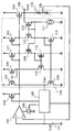
- FIG. 1 is a circuit diagram of a voltage regulator including the overshoot suppression circuit of the present embodiment.
- the voltage regulator of this embodiment includes a reference voltage circuit 101, an error amplification circuit 102, a bias circuit 103 of the error amplification circuit 102, an output transistor 104, a voltage dividing resistor circuit 105, and a non-regulated state detection circuit 106. , An overshoot control circuit 107 and a PMOS transistor 108 are provided. The non-regulated state detection circuit 106 and the overshoot control circuit 107 constitute an overshoot suppression circuit.
- the voltage dividing resistor circuit 105 is connected between the output terminal 109 and the ground terminal.
- the error amplification circuit 102 inputs the feedback voltage Vfb to the non-inverting input terminal and inputs the reference voltage Vref to the inverting input terminal.
- the output transistor 104 has a gate connected to the output terminal of the error amplifier circuit 102, a source connected to the power supply terminal, and a drain connected to the output terminal 109.
- the non-regulated state detection circuit 106 receives the voltage of the output terminal 109 and the voltage of the power supply terminal, and the output terminal is connected to the overshoot control circuit 107.
- the overshoot control circuit 107 receives the feedback voltage Vfb and the reference voltage Vref, and has an output terminal connected to the bias circuit 103 and the gate of the PMOS transistor 108.
- the voltage dividing resistor circuit 105 divides the output voltage Vout of the output terminal 109 and outputs a feedback voltage Vfb.
- the error amplifier circuit 102 compares the reference voltage Vref output from the reference voltage circuit 101 with the feedback voltage Vfb.
- the output transistor 104 is controlled by the output voltage of the error amplifier circuit 102 and has a function of keeping the voltage of the output terminal 109 constant.
- the non-regulated state detection circuit 106 detects a non-regulated state based on the current flowing through the output transistor 104 and the output voltage Vout of the output terminal 109.
- the overshoot control circuit 107 detects an overshoot of the output terminal 109 based on the reference voltage Vref and the feedback voltage Vfb, and controls the PMOS transistor 108 and the bias circuit 103.
- the overshoot control circuit 107 receives the detection signal Vdet from the non-regulated state detection circuit 106 and controls the operating current of the overshoot control circuit 107.
- the overshoot control circuit 107 includes a circuit as shown in FIG. 3 as an example.
- the overshoot control circuit 107 shown in FIG. 3 receives an amplifier 301 to which the reference voltage Vref and the feedback voltage Vfb are input, and a bias for controlling the operating current of the amplifier 301 by inputting the detection signal Vdet of the non-regulated state detection circuit 106.
- a circuit 302 is provided.
- the overshoot control circuit 107 may be a circuit for realizing the function of detecting the overshoot of the output terminal 109, and the circuit configuration is not particularly limited.
- the bias circuit 103 may be a constant current circuit that receives a signal from the overshoot control circuit 107 and increases the current, and the circuit configuration is not particularly limited.
- the non-regulated state detection circuit 106 includes PMOS transistors 110, 112, 113, 116, 117, 120, 121, NMOS transistors 114, 115, 118, 119, and a constant current source 111.
- the PMOS transistor 110 has a source connected to the output terminal 109 and a gate and drain connected to the constant current source 111.
- the PMOS transistor 112 has a source connected to the drain of the PMOS transistor 113, a gate connected to the gate and drain of the PMOS transistor 110, and a drain connected to the gate and drain of the NMOS transistor 114.
- the PMOS transistor 113 has a source connected to the power supply terminal and a gate connected to the output terminal of the error amplifier circuit 102.
- the NMOS transistor 114 has a source connected to the ground terminal, and a gate and a drain connected to the gate of the NMOS transistor 115.
- the PMOS transistor 116 has a source connected to the drain of the PMOS transistor 117, a gate connected to the gate and drain of the PMOS transistor 110, and a drain connected to the gate and drain of the NMOS transistor 118.
- the PMOS transistor 117 has a source connected to the power supply terminal and a gate connected to the output terminal of the error amplifier circuit 102.
- the NMOS transistor 118 has a source connected to the ground terminal, and a gate and a drain connected to the gate of the NMOS transistor 119.
- the NMOS transistor 119 has a source connected to the ground terminal and a drain connected to the gate and drain of the PMOS transistor 120.
- the PMOS transistor 120 has a source connected to the power supply terminal and a gate and a drain connected to the gate of the PMOS transistor 121.
- the PMOS transistor 121 and the NMOS transistor 115 are connected between the power supply terminal and the ground terminal, and the connection node is an output terminal of the non-regulated state detection circuit 106.
- the PMOS transistor 110 and the constant current source 111 detect the state of the output terminal 109.
- the PMOS transistor 112, the PMOS transistor 113, and the NMOS transistor 114 constitute a first detection circuit, and the detection result is output to the gate of the NMOS transistor 115.
- the PMOS transistor 116, the PMOS transistor 117, the NMOS transistor 118, and the NMOS transistor 119 and the PMOS transistor 120 constitute a second detection circuit, and output the detection result to the gate of the PMOS transistor 121.
- the current that flows is changed according to the signal input to the gate, and the signal Vdet is output to the output terminal of the non-regulated state detection circuit 106 due to the balance.
- the overshoot suppression circuit as described above operates as follows to suppress overshoot of the output terminal 109.
- a state where the power supply voltage is sufficiently high and the output voltage Vout of the output terminal 109 is close to a predetermined voltage is defined as a normal state.
- a state where the power supply voltage is low and the output terminal 109 outputs a voltage lower than the predetermined output voltage Vout is defined as a non-regulated state.
- Each transistor of the non-regulated state detection circuit 106 is designed as follows, for example.
- the PMOS transistor 113 and the PMOS transistor 117 that mirror the current of the output transistor 104 are designed so that the mirror ratio of the PMOS transistor 113 is larger.
- the PMOS transistor 112 and the PMOS transistor 116 that mirror the current of the PMOS transistor 110 are designed to have a larger mirror ratio than the PMOS transistor 116.
- the current flowing through the PMOS transistor 112 and the PMOS transistor 116 is designed to be sufficiently larger than the current flowing through the PMOS transistor 113 and the PMOS transistor 117.
- the non-regulated state detection circuit 106 outputs the Lo signal Vdet to the output terminal, indicating that the output transistor 104 is in a saturated state.
- the overshoot control circuit 107 receives the Lo signal Vdet, reduces the operating current, and enters the normal state.
- the difference between the power supply voltage and the output voltage Vout becomes small. Since the output voltage Vout is low, the PMOS transistor 113 and the PMOS transistor 117 are turned on when the Lo voltage is input to their gates. Therefore, the drain voltages of the PMOS transistor 113 and the PMOS transistor 117 become the power supply voltage. That is, the drain voltages of the PMOS transistor 113 and the PMOS transistor 117 are close to the output voltage Vout.
- the PMOS transistor 110 has a low output voltage Vout, but the current flowing through the bias circuit 111 is sufficiently small, so that current can flow. Therefore, the gate voltage of the PMOS transistor 110 becomes a voltage corresponding to the impedance of the bias circuit 111 and the PMOS transistor 110 and the output voltage Vout.
- the gate voltages of the PMOS transistor 112 and the PMOS transistor 116 are equal to the gate voltage of the PMOS transistor 110.
- the source voltages of the PMOS transistor 112 and the PMOS transistor 116 are voltages determined by the gate voltage of the PMOS transistor 110 and the threshold values of the PMOS transistor 112 and the PMOS transistor 116.
- the non-regulated state detection circuit 106 Indicates that the Hi signal Vdet is output to the output terminal, indicating that the voltage regulator is in a non-regulated state.
- the overshoot control circuit 107 receives the Hi signal Vdet, increases the operating current, and enters a high-speed operating state. Therefore, even if the power supply voltage increases from this state and an overshoot occurs at the output terminal 109, the overshoot control circuit 107 can quickly detect the overshoot and control the bias circuit 103 and the PMOS transistor 108. I can do it. And overshoot of the output terminal 109 can be suppressed.
- the overshoot suppression circuit of the voltage regulator according to the present embodiment is in a low consumption state in which the operation current of the overshoot control circuit 107 is low in the normal state, and thus it is possible to reduce the consumption current. . Further, when the non-regulated state detection circuit 106 detects the non-regulated state of the voltage regulator, the operating current of the overshoot control circuit 107 is increased, so that overshoot of the output terminal 109 can be suppressed quickly.
- FIG. 2 shows a circuit diagram of the voltage regulator of the second embodiment. In the voltage regulator of the second embodiment, the non-regulated state detection circuit 106 is configured as follows.
- the first detection circuit includes a PMOS transistor 112, a PMOS transistor 113, and a resistor 202.
- the second detection circuit includes a PMOS transistor 116, a PMOS transistor 117, and a resistor 203.
- the output terminal of the comparison circuit 201 to which each detection result is input constitutes the output terminal of the non-regulated state detection circuit 106.
- the voltage regulator according to the present embodiment has been described as a configuration in which when the overshoot is detected, the current of the output transistor 104 is decreased by the signal of the overshoot control circuit 107 and the current of the bias circuit 103 is increased.
- the signal of the overshoot control circuit 107 it has an effect of suppressing the overshoot and is not particularly limited thereto.
Landscapes
- Engineering & Computer Science (AREA)
- Physics & Mathematics (AREA)
- Electromagnetism (AREA)
- General Physics & Mathematics (AREA)
- Radar, Positioning & Navigation (AREA)
- Automation & Control Theory (AREA)
- Power Engineering (AREA)
- Continuous-Control Power Sources That Use Transistors (AREA)
Description
本発明は、ボルテージレギュレータのオーバーシュート抑制回路に関する。
従来のボルテージレギュレータについて説明する。図4は、従来のボルテージレギュレータを示す回路図である。
従来のボルテージレギュレータは、基準電圧回路101と、誤差増幅回路102と、誤差増幅回路102のバイアス回路103と、出力トランジスタであるPMOSトランジスタ104と、分圧抵抗回路105と、アンプ301と、アンプ301のバイアス回路302と、PMOSトランジスタ108を備えている。
PMOSトランジスタ104は、電源端子と出力端子109の間に接続される。フィードバック電圧Vfbを出力する分圧抵抗回路105は、出力端子109と接地端子の間に接続される。誤差増幅回路102は、反転入力端子に基準電圧回路101が接続され、非反転入力端子にフィードバック電圧Vfbが入力され、出力端子はPMOSトランジスタ104のゲートに接続される。バイアス回路103は、誤差増幅回路102に動作電流を供給する。PMOSトランジスタ108は、電源端子とPMOSトランジスタ104のゲートの間に接続される。アンプ301は、非反転入力端子に基準電圧回路101が接続され、反転入力端子にフィードバック電圧Vfbが入力され、出力端子はPMOSトランジスタ108のゲートに接続される。バイアス回路302は、アンプ301に動作電流を供給する。
アンプ301は、入力されたフィードバック電圧Vfbと基準電圧Vrefとを比較する。フィードバック電圧Vfbが基準電圧Vrefより低い場合、アンプ301はHi信号を出力してPMOSトランジスタ108をオフさせる。出力端子109の出力電圧Voutにオーバーシュートが発生し、フィードバック電圧Vfbが基準電圧Vrefよりも高くなると、アンプ301はLo信号を出力してPMOSトランジスタ108をオンさせる。
従来のボルテージレギュレータは、このように動作して、出力端子109の出力電圧Voutのオーバーシュートが大きくなることを防ぐことができる(例えば、特許文献1参照)。
しかしながら、従来のボルテージレギュレータは、電源電圧が低く、出力端子109が所定の出力電圧Voutより低い電圧を出力している状態(以下、非レギュレート状態)において、電源電圧が高くなった時に出力端子109に過大なオーバーシュートが生じるという課題があった。また、過大なオーバーシュートを防止するためには、アンプ301のバイアス回路302が流す電流を多くする必要があるが、そのためボルテージレギュレータの消費電流が多くなると言う課題があった。
本発明は、上記課題に鑑みてなされ、低消費電流でありながら、非レギュレート状態において電源電圧が高くなった時に出力端子に過大なオーバーシュートが発生することを抑制できるボルテージレギュレータを提供する。
従来の課題を解決するために、本発明のオーバーシュート抑制回路を備えたボルテージレギュレータは以下のような構成とした。
出力電圧にオーバーシュートが発生したことを検出し、出力トランジスタの電流を制限するオーバーシュート制限回路と、出力端子の電圧と出力トランジスタに流れる電流に基づいて、ボルテージレギュレータが非レギュレート状態であることを検出する非レギュレート状態検出回路を備え、オーバーシュート制限回路は、非レギュレート状態検出回路の検出信号によって動作電流を制御される、ことを特徴とするボルテージレギュレータ。
本発明のオーバーシュート抑制回路を備えたボルテージレギュレータは、低消費電流で、非レギュレート状態で電源電圧が高くなった時に発生する出力電圧のオーバーシュートを抑制できる、と言う効果がある。
以下、本実施形態について、図面を参照して説明する。
[第1の実施形態]
図1は、本実施形態のオーバーシュート抑制回路を備えたボルテージレギュレータの回路図である。
[第1の実施形態]
図1は、本実施形態のオーバーシュート抑制回路を備えたボルテージレギュレータの回路図である。
本実施形態のボルテージレギュレータは、基準電圧回路101と、誤差増幅回路102と、誤差増幅回路102のバイアス回路103と、出力トランジスタ104と、分圧抵抗回路105と、非レギュレート状態検出回路106と、オーバーシュート制御回路107と、PMOSトランジスタ108を備えている。非レギュレート状態検出回路106とオーバーシュート制御回路107は、オーバーシュート抑制回路を構成する。
分圧抵抗回路105は、出力端子109と接地端子の間に接続される。誤差増幅回路102は、非反転入力端子にフィードバック電圧Vfbを入力し、反転入力端子に基準電圧Vrefを入力する。出力トランジスタ104は、ゲートに誤差増幅回路102の出力端子を接続し、ソースを電源端子に接続し、ドレインを出力端子109に接続する。非レギュレート状態検出回路106は、出力端子109の電圧と電源端子の電圧が入力され、出力端子がオーバーシュート制御回路107に接続されている。オーバーシュート制御回路107は、フィードバック電圧Vfbと基準電圧Vrefを入力し、出力端子がバイアス回路103とPMOSトランジスタ108のゲートに接続されている。
分圧抵抗回路105は、出力端子109の出力電圧Voutを分圧し、フィードバック電圧Vfbを出力する。誤差増幅回路102は、基準電圧回路101の出力する基準電圧Vrefとフィードバック電圧Vfbを比較する。出力トランジスタ104は、誤差増幅回路102の出力電圧によって制御され、出力端子109の電圧を一定に保つ機能を有する。非レギュレート状態検出回路106は、出力トランジスタ104に流れる電流と出力端子109の出力電圧Voutに基づいて非レギュレート状態を検出する。オーバーシュート制御回路107は、基準電圧Vrefとフィードバック電圧Vfbに基づいて出力端子109のオーバーシュートを検出して、PMOSトランジスタ108とバイアス回路103を制御する。オーバーシュート制御回路107は、非レギュレート状態検出回路106の検出信号Vdetを受けて、オーバーシュート制御回路107の動作電流を制御する。
オーバーシュート制御回路107は、一例として図3に示すような回路で構成される。図3に示すオーバーシュート制御回路107は、基準電圧Vrefとフィードバック電圧Vfbが入力されるアンプ301と、非レギュレート状態検出回路106の検出信号Vdetを入力してアンプ301の動作電流を制御するバイアス回路302を備えている。
但し、オーバーシュート制御回路107は、出力端子109のオーバーシュートを検出する機能を実現するための回路であればよく、回路構成は特に限定されるものではない。また、バイアス回路103は、オーバーシュート制御回路107の信号を受けて電流を増加するような定電流回路であればよく、回路構成は特に限定されるものではない。
非レギュレート状態検出回路106は、PMOSトランジスタ110、112、113、116、117、120、121と、NMOSトランジスタ114、115、118、119と、定電流源111を備えている。
PMOSトランジスタ110は、ソースが出力端子109に接続され、ゲートとドレインが定電流源111に接続されている。PMOSトランジスタ112は、ソースがPMOSトランジスタ113のドレインに接続され、ゲートがPMOSトランジスタ110のゲートとドレインに接続され、ドレインがNMOSトランジスタ114のゲートとドレインに接続されている。PMOSトランジスタ113は、ソースが電源端子に接続され、ゲートが誤差増幅回路102の出力端子に接続されている。NMOSトランジスタ114は、ソースが接地端子に接続され、ゲートとドレインがNMOSトランジスタ115のゲートに接続されている。PMOSトランジスタ116は、ソースがPMOSトランジスタ117のドレインに接続され、ゲートがPMOSトランジスタ110のゲートとドレインに接続され、ドレインがNMOSトランジスタ118のゲートとドレインに接続されている。PMOSトランジスタ117は、ソースが電源端子に接続され、ゲートが誤差増幅回路102の出力端子に接続されている。NMOSトランジスタ118は、ソースが接地端子に接続され、ゲートとドレインがNMOSトランジスタ119のゲートに接続されている。NMOSトランジスタ119は、ソースが接地端子に接続され、ドレインがPMOSトランジスタ120のゲートとドレインに接続されている。PMOSトランジスタ120は、ソースが電源端子に接続され、ゲートとドレインがPMOSトランジスタ121のゲートに接続されている。PMOSトランジスタ121とNMOSトランジスタ115は、電源端子と接地端子の間に接続され、その接続ノードは非レギュレート状態検出回路106の出力端子になっている。
PMOSトランジスタ110と定電流源111は、出力端子109の状態を検出する。PMOSトランジスタ112とPMOSトランジスタ113とNMOSトランジスタ114は、第一の検出回路を構成し、その検出結果をNMOSトランジスタ115のゲートに出力する。PMOSトランジスタ116とPMOSトランジスタ117とNMOSトランジスタ118、及びNMOSトランジスタ119とPMOSトランジスタ120は、第二の検出回路を構成し、その検出結果をPMOSトランジスタ121のゲートに出力する。PMOSトランジスタ121とNMOSトランジスタ115は、ゲートに入力される信号によって流す電流が変化し、そのバランスによって非レギュレート状態検出回路106の出力端子に信号Vdetが出力される。
上述したようなオーバーシュート抑制回路は、以下のように動作して出力端子109のオーバーシュートを抑制する。
電源電圧が十分高く、出力端子109の出力電圧Voutが所定の電圧に近い状態を通常状態とする。電源電圧が低く、出力端子109が所定の出力電圧Voutより低い電圧を出力している状態を非レギュレート状態とする。
非レギュレート状態検出回路106の各トランジスタは、例えば以下のように設計される。
出力トランジスタ104の電流をミラーするPMOSトランジスタ113とPMOSトランジスタ117は、PMOSトランジスタ113の方のミラー比を大きく設計する。PMOSトランジスタ110の電流をミラーするPMOSトランジスタ112とPMOSトランジスタ116は、PMOSトランジスタ116の方のミラー比を大きく設計する。通常状態では、PMOSトランジスタ112とPMOSトランジスタ116が流す電流は、PMOSトランジスタ113とPMOSトランジスタ117が流す電流より十分多くなるように設計する。
通常動作状態において、PMOSトランジスタ113がPMOSトランジスタ117より多く電流を流す。それらの電流をミラーした結果、NMOSトランジスタ115がPMOSトランジスタ121より多く電流を流す。従って、非レギュレート状態検出回路106は、出力端子にLoの信号Vdetを出力し、出力トランジスタ104が飽和状態にあることを示す。
オーバーシュート制御回路107は、Loの信号Vdetを受けて、動作電流を少なくして、通常状態になる。
ボルテージレギュレータが非レギュレート状態になると、電源電圧と出力電圧Voutの差が小さくなる。PMOSトランジスタ113とPMOSトランジスタ117は、出力電圧Voutが低くいので、ゲートにLoの電圧が入力されオンする。従って、PMOSトランジスタ113とPMOSトランジスタ117のドレイン電圧は、電源電圧になる。すなわち、PMOSトランジスタ113とPMOSトランジスタ117のドレイン電圧は、出力電圧Voutに近くなる。PMOSトランジスタ110は、出力電圧Voutが低くなるが、バイアス回路111の流す電流は十分少ないので、電流を流すことが出来る。従って、PMOSトランジスタ110のゲート電圧は、バイアス回路111とPMOSトランジスタ110のインピーダンスと出力電圧Voutに応じた電圧になる。そして、PMOSトランジスタ112とPMOSトランジスタ116のゲート電圧は、PMOSトランジスタ110のゲート電圧に等しい。また、PMOSトランジスタ112とPMOSトランジスタ116のソース電圧は、PMOSトランジスタ110のゲート電圧とPMOSトランジスタ112とPMOSトランジスタ116の閾値で決まる電圧になっている。
このような状態では、PMOSトランジスタ112とPMOSトランジスタ116が流す電流は、PMOSトランジスタ113とPMOSトランジスタ117が流す電流より少なくなる。従って、PMOSトランジスタ116は、PMOSトランジスタ112よりもミラー比を大きいので、PMOSトランジスタ116がPMOSトランジスタ112より多く電流を流す。それらの電流をミラーした結果、PMOSトランジスタ121がNMOSトランジスタ115より多く電流を流す。従って、非レギュレート状態検出回路106
は、出力端子にHiの信号Vdetを出力し、ボルテージレギュレータが非レギュレート状態にあることを示す。
は、出力端子にHiの信号Vdetを出力し、ボルテージレギュレータが非レギュレート状態にあることを示す。
オーバーシュート制御回路107は、Hiの信号Vdetを受けて、動作電流を多くして、高速動作状態になる。従って、この状態から電源電圧が高くなって、出力端子109にオーバーシュートが発生しても、オーバーシュート制御回路107は素早くオーバーシュートを検出して、バイアス回路103とPMOSトランジスタ108を制御することが出来る。そして、出力端子109のオーバーシュートを抑制することが出来る。
以上記載したように、本実施形態のボルテージレギュレータのオーバーシュート抑制回路は、通常状態ではオーバーシュート制御回路107の動作電流の少ない低消費状態になるため、消費電流を少なくすることが可能となった。また、非レギュレート状態検出回路106がボルテージレギュレータの非レギュレート状態を検出すると、オーバーシュート制御回路107の動作電流を多くするので、素早く出力端子109のオーバーシュートを抑制することが出来る。
[第2の実施形態]
図2に、第2の実施形態のボルテージレギュレータの回路図を示す。第2の実施形態のボルテージレギュレータは、非レギュレート状態検出回路106を以下に示すように構成する。
[第2の実施形態]
図2に、第2の実施形態のボルテージレギュレータの回路図を示す。第2の実施形態のボルテージレギュレータは、非レギュレート状態検出回路106を以下に示すように構成する。
第一の検出回路は、PMOSトランジスタ112とPMOSトランジスタ113と抵抗202で構成する。第二の検出回路は、PMOSトランジスタ116とPMOSトランジスタ117と抵抗203で構成する。それぞれの検出結果が入力される比較回路201の出力端子が、非レギュレート状態検出回路106の出力端子を構成する。
このような回路構成としても、第1の実施形態と同様の効果を得ることが出来る。
以上に説明したように、本実施形態のボルテージレギュレータによれば、通常状態において、オーバーシュート抑制回路に不必要な電流が流れることがなくなり、消費電流を少なくすることが出来るという効果がある。
なお本の実施形態のボルテージレギュレータは、オーバーシュートを検出したときに、オーバーシュート制御回路107の信号によって、出力トランジスタ104の電流を減少させ、バイアス回路103の電流を増加させる構成として説明した。しかし、オーバーシュート制御回路107の信号によって、どちらかのみを制御する構成であっても、オーバーシュートを抑制する効果を有するので、特にそれに限定されるものではない。
101 基準電圧回路
102 誤差増幅回路
103、111 バイアス回路
105 分圧抵抗回路
107 オーバーシュート制御回路
201 比較回路
102 誤差増幅回路
103、111 バイアス回路
105 分圧抵抗回路
107 オーバーシュート制御回路
201 比較回路
Claims (3)
- 出力トランジスタが出力する出力電圧を分圧した分圧電圧と基準電圧の差を増幅して出力し、前記出力トランジスタのゲートを制御する誤差増幅回路と、
前記出力電圧にオーバーシュートが発生したことを検出し、前記出力トランジスタの電流を制限するオーバーシュート制限回路と、
前記出力電圧と前記出力トランジスタに流れる電流に基づいて、ボルテージレギュレータが非レギュレート状態であることを検出する非レギュレート状態検出回路と、を備え、
前記オーバーシュート制限回路は、前記非レギュレート状態検出回路の検出信号によって動作電流を制御される、
ことを特徴とするボルテージレギュレータ。 - 前記非レギュレート状態検出回路は、
第一の検出回路及び第二の検出回路と
前記第一の検出回路と前記第二の検出回路の出力を入力し、検出信号を出力する出力回路と、を備え、
通常状態では、前記第一の検出回路が前記第二の検出回路よりも多く電流を流し、
非レギュレート状態では、前記第二の検出回路が前記第一の検出回路よりも多く電流を流し、
前記出力回路は、前記第一の検出回路の電流と前記第二の検出回路の電流に応じて、検出信号を出力する、
ことを特徴とする請求項1に記載のボルテージレギュレータ。 - 前記第一の検出回路と前記第二の検出回路は、電流を電圧に変換する回路を備え、
前記出力回路は、前記第一の検出回路の電流を変換した電圧と前記第二の検出回路の電流を変換した電圧に応じて、検出信号を出力する、
ことを特徴とする請求項2に記載のボルテージレギュレータ。
Priority Applications (4)
| Application Number | Priority Date | Filing Date | Title |
|---|---|---|---|
| EP13835676.1A EP2894537B1 (en) | 2012-09-07 | 2013-07-10 | Voltage regulator |
| CN201380046042.2A CN104603710B (zh) | 2012-09-07 | 2013-07-10 | 稳压器 |
| KR1020157005713A KR102052896B1 (ko) | 2012-09-07 | 2013-07-10 | 볼티지 레귤레이터 |
| US14/639,681 US9323258B2 (en) | 2012-09-07 | 2015-03-05 | Voltage regulator |
Applications Claiming Priority (2)
| Application Number | Priority Date | Filing Date | Title |
|---|---|---|---|
| JP2012-197541 | 2012-09-07 | ||
| JP2012197541A JP6130112B2 (ja) | 2012-09-07 | 2012-09-07 | ボルテージレギュレータ |
Related Child Applications (1)
| Application Number | Title | Priority Date | Filing Date |
|---|---|---|---|
| US14/639,681 Continuation US9323258B2 (en) | 2012-09-07 | 2015-03-05 | Voltage regulator |
Publications (1)
| Publication Number | Publication Date |
|---|---|
| WO2014038284A1 true WO2014038284A1 (ja) | 2014-03-13 |
Family
ID=50236902
Family Applications (1)
| Application Number | Title | Priority Date | Filing Date |
|---|---|---|---|
| PCT/JP2013/068815 Ceased WO2014038284A1 (ja) | 2012-09-07 | 2013-07-10 | ボルテージレギュレータ |
Country Status (7)
| Country | Link |
|---|---|
| US (1) | US9323258B2 (ja) |
| EP (1) | EP2894537B1 (ja) |
| JP (1) | JP6130112B2 (ja) |
| KR (1) | KR102052896B1 (ja) |
| CN (1) | CN104603710B (ja) |
| TW (1) | TWI582562B (ja) |
| WO (1) | WO2014038284A1 (ja) |
Cited By (2)
| Publication number | Priority date | Publication date | Assignee | Title |
|---|---|---|---|---|
| CN105717971A (zh) * | 2014-12-19 | 2016-06-29 | 精工半导体有限公司 | 电压调节器 |
| US10048717B1 (en) | 2017-08-17 | 2018-08-14 | Powerchip Technology Corporation | Voltage regulation device capable of stabilizing output voltage |
Families Citing this family (16)
| Publication number | Priority date | Publication date | Assignee | Title |
|---|---|---|---|---|
| CN104142701B (zh) | 2013-05-06 | 2016-08-24 | 意法半导体研发(深圳)有限公司 | 限流电路 |
| JP6170354B2 (ja) * | 2013-06-25 | 2017-07-26 | エスアイアイ・セミコンダクタ株式会社 | ボルテージレギュレータ |
| CN104423407B (zh) | 2013-08-28 | 2016-05-25 | 联发科技(新加坡)私人有限公司 | 低压差线性稳压器及其启动方法、电子装置和芯片 |
| DE102015216928B4 (de) | 2015-09-03 | 2021-11-04 | Dialog Semiconductor (Uk) Limited | Regler mit Überspannungsklemme und entsprechende Verfahren |
| US9645594B2 (en) * | 2015-10-13 | 2017-05-09 | STMicroelectronics Design & Application S.R.O. | Voltage regulator with dropout detector and bias current limiter and associated methods |
| TWI645279B (zh) | 2016-11-15 | 2018-12-21 | 瑞昱半導體股份有限公司 | 參考電壓緩衝電路 |
| JP6763763B2 (ja) * | 2016-12-22 | 2020-09-30 | 新日本無線株式会社 | 電源回路 |
| US10031541B1 (en) * | 2017-07-05 | 2018-07-24 | Infineon Technologies Ag | Current sensing for linear voltage regulator |
| KR101937268B1 (ko) * | 2017-10-11 | 2019-04-09 | 현대오트론 주식회사 | 실시간 기울기 제어 장치 및 그것의 동작 방법 |
| JP6986999B2 (ja) * | 2018-03-15 | 2021-12-22 | エイブリック株式会社 | ボルテージレギュレータ |
| JP7065660B2 (ja) * | 2018-03-22 | 2022-05-12 | エイブリック株式会社 | ボルテージレギュレータ |
| CN110134176B (zh) * | 2018-09-05 | 2024-05-28 | 江西联智集成电路有限公司 | Ldo电路及无线充电系统 |
| JP6669917B2 (ja) * | 2019-04-10 | 2020-03-18 | エイブリック株式会社 | ボルテージレギュレータ |
| CN110221647B (zh) * | 2019-06-28 | 2020-09-08 | 上海视欧光电科技有限公司 | 一种稳压器 |
| JP7391791B2 (ja) * | 2020-08-12 | 2023-12-05 | 株式会社東芝 | 定電圧回路 |
| JP7715563B2 (ja) * | 2021-07-27 | 2025-07-30 | ローム株式会社 | リニアレギュレータ回路 |
Citations (6)
| Publication number | Priority date | Publication date | Assignee | Title |
|---|---|---|---|---|
| JP2001022455A (ja) * | 1999-07-09 | 2001-01-26 | New Japan Radio Co Ltd | レギュレータ回路 |
| JP2003330555A (ja) * | 2002-05-14 | 2003-11-21 | Renesas Technology Corp | 半導体集積回路およびicカード |
| JP2005301439A (ja) | 2004-04-07 | 2005-10-27 | Ricoh Co Ltd | ボルテージレギュレータ |
| JP2006301787A (ja) * | 2005-04-18 | 2006-11-02 | Ricoh Co Ltd | 定電圧電源回路 |
| JP2009146130A (ja) * | 2007-12-13 | 2009-07-02 | Oki Semiconductor Co Ltd | ドロッパ型レギュレータ |
| JP2009199501A (ja) * | 2008-02-25 | 2009-09-03 | Seiko Instruments Inc | ボルテージレギュレータ |
Family Cites Families (12)
| Publication number | Priority date | Publication date | Assignee | Title |
|---|---|---|---|---|
| DE3723579C1 (de) * | 1987-07-16 | 1989-02-16 | Sgs Halbleiterbauelemente Gmbh | Laengsspannungsregler |
| JP2001306163A (ja) * | 2000-04-27 | 2001-11-02 | Matsushita Electric Ind Co Ltd | アナログmosによる過電流保護機能付きレギュレータ回路 |
| JP4050671B2 (ja) * | 2003-01-08 | 2008-02-20 | 株式会社リコー | 定電圧回路 |
| US7215180B2 (en) * | 2003-08-07 | 2007-05-08 | Ricoh Company, Ltd. | Constant voltage circuit |
| JP2006139673A (ja) * | 2004-11-15 | 2006-06-01 | Seiko Instruments Inc | ボルテージレギュレータ |
| JP4892366B2 (ja) * | 2007-02-01 | 2012-03-07 | セイコーインスツル株式会社 | 過電流保護回路およびボルテージレギュレータ |
| JP4953246B2 (ja) * | 2007-04-27 | 2012-06-13 | セイコーインスツル株式会社 | ボルテージレギュレータ |
| JP4929043B2 (ja) * | 2007-05-15 | 2012-05-09 | 株式会社リコー | 過電流保護回路および該過電流保護回路を備えた電子機器 |
| JP2009176008A (ja) * | 2008-01-24 | 2009-08-06 | Seiko Instruments Inc | ボルテージレギュレータ |
| JP5421133B2 (ja) * | 2009-02-10 | 2014-02-19 | セイコーインスツル株式会社 | ボルテージレギュレータ |
| JP5279544B2 (ja) * | 2009-02-17 | 2013-09-04 | セイコーインスツル株式会社 | ボルテージレギュレータ |
| JP5828206B2 (ja) * | 2011-01-24 | 2015-12-02 | 凸版印刷株式会社 | 定電圧回路 |
-
2012
- 2012-09-07 JP JP2012197541A patent/JP6130112B2/ja not_active Expired - Fee Related
-
2013
- 2013-07-10 KR KR1020157005713A patent/KR102052896B1/ko not_active Expired - Fee Related
- 2013-07-10 WO PCT/JP2013/068815 patent/WO2014038284A1/ja not_active Ceased
- 2013-07-10 EP EP13835676.1A patent/EP2894537B1/en active Active
- 2013-07-10 CN CN201380046042.2A patent/CN104603710B/zh not_active Expired - Fee Related
- 2013-07-22 TW TW102126099A patent/TWI582562B/zh not_active IP Right Cessation
-
2015
- 2015-03-05 US US14/639,681 patent/US9323258B2/en not_active Expired - Fee Related
Patent Citations (6)
| Publication number | Priority date | Publication date | Assignee | Title |
|---|---|---|---|---|
| JP2001022455A (ja) * | 1999-07-09 | 2001-01-26 | New Japan Radio Co Ltd | レギュレータ回路 |
| JP2003330555A (ja) * | 2002-05-14 | 2003-11-21 | Renesas Technology Corp | 半導体集積回路およびicカード |
| JP2005301439A (ja) | 2004-04-07 | 2005-10-27 | Ricoh Co Ltd | ボルテージレギュレータ |
| JP2006301787A (ja) * | 2005-04-18 | 2006-11-02 | Ricoh Co Ltd | 定電圧電源回路 |
| JP2009146130A (ja) * | 2007-12-13 | 2009-07-02 | Oki Semiconductor Co Ltd | ドロッパ型レギュレータ |
| JP2009199501A (ja) * | 2008-02-25 | 2009-09-03 | Seiko Instruments Inc | ボルテージレギュレータ |
Non-Patent Citations (1)
| Title |
|---|
| See also references of EP2894537A4 |
Cited By (4)
| Publication number | Priority date | Publication date | Assignee | Title |
|---|---|---|---|---|
| CN105717971A (zh) * | 2014-12-19 | 2016-06-29 | 精工半导体有限公司 | 电压调节器 |
| CN105717971B (zh) * | 2014-12-19 | 2018-11-09 | 艾普凌科有限公司 | 电压调节器 |
| US10048717B1 (en) | 2017-08-17 | 2018-08-14 | Powerchip Technology Corporation | Voltage regulation device capable of stabilizing output voltage |
| TWI633408B (zh) * | 2017-08-17 | 2018-08-21 | 力晶科技股份有限公司 | 穩壓輸出裝置 |
Also Published As
| Publication number | Publication date |
|---|---|
| JP6130112B2 (ja) | 2017-05-17 |
| CN104603710A (zh) | 2015-05-06 |
| US20150177752A1 (en) | 2015-06-25 |
| JP2014052886A (ja) | 2014-03-20 |
| EP2894537A4 (en) | 2016-04-27 |
| CN104603710B (zh) | 2016-10-12 |
| TW201423302A (zh) | 2014-06-16 |
| EP2894537B1 (en) | 2020-02-26 |
| KR102052896B1 (ko) | 2019-12-06 |
| TWI582562B (zh) | 2017-05-11 |
| EP2894537A1 (en) | 2015-07-15 |
| US9323258B2 (en) | 2016-04-26 |
| KR20150048763A (ko) | 2015-05-07 |
Similar Documents
| Publication | Publication Date | Title |
|---|---|---|
| JP6130112B2 (ja) | ボルテージレギュレータ | |
| TWI585565B (zh) | 電壓調節器 | |
| JP4953246B2 (ja) | ボルテージレギュレータ | |
| JP6416638B2 (ja) | ボルテージレギュレータ | |
| JP5977963B2 (ja) | ボルテージレギュレータ | |
| JP6261343B2 (ja) | ボルテージレギュレータ | |
| KR102225712B1 (ko) | 볼티지 레귤레이터 | |
| JP2012159870A (ja) | ボルテージレギュレータ | |
| TWI801493B (zh) | 電壓調整器 | |
| KR102279836B1 (ko) | 과전류 보호 회로, 반도체 장치 및 볼티지 레귤레이터 | |
| JP2017126259A (ja) | 電源装置 | |
| TWI628528B (zh) | 電壓產生器 | |
| CN110121685B (zh) | 电源电路 | |
| JP4892366B2 (ja) | 過電流保護回路およびボルテージレギュレータ | |
| US20130241508A1 (en) | Voltage regulator | |
| JP2017129929A (ja) | ボルテージレギュレータ |
Legal Events
| Date | Code | Title | Description |
|---|---|---|---|
| 121 | Ep: the epo has been informed by wipo that ep was designated in this application |
Ref document number: 13835676 Country of ref document: EP Kind code of ref document: A1 |
|
| ENP | Entry into the national phase |
Ref document number: 20157005713 Country of ref document: KR Kind code of ref document: A |
|
| NENP | Non-entry into the national phase |
Ref country code: DE |