WO2014041821A1 - 光合分波器 - Google Patents
光合分波器 Download PDFInfo
- Publication number
- WO2014041821A1 WO2014041821A1 PCT/JP2013/005463 JP2013005463W WO2014041821A1 WO 2014041821 A1 WO2014041821 A1 WO 2014041821A1 JP 2013005463 W JP2013005463 W JP 2013005463W WO 2014041821 A1 WO2014041821 A1 WO 2014041821A1
- Authority
- WO
- WIPO (PCT)
- Prior art keywords
- waveguide
- input
- output
- demultiplexer
- slab
- Prior art date
- Legal status (The legal status is an assumption and is not a legal conclusion. Google has not performed a legal analysis and makes no representation as to the accuracy of the status listed.)
- Ceased
Links
Images



Classifications
-
- H—ELECTRICITY
- H04—ELECTRIC COMMUNICATION TECHNIQUE
- H04B—TRANSMISSION
- H04B10/00—Transmission systems employing electromagnetic waves other than radio-waves, e.g. infrared, visible or ultraviolet light, or employing corpuscular radiation, e.g. quantum communication
- H04B10/40—Transceivers
-
- G—PHYSICS
- G02—OPTICS
- G02B—OPTICAL ELEMENTS, SYSTEMS OR APPARATUS
- G02B6/00—Light guides; Structural details of arrangements comprising light guides and other optical elements, e.g. couplings
- G02B6/10—Light guides; Structural details of arrangements comprising light guides and other optical elements, e.g. couplings of the optical waveguide type
- G02B6/12—Light guides; Structural details of arrangements comprising light guides and other optical elements, e.g. couplings of the optical waveguide type of the integrated circuit kind
- G02B6/12007—Light guides; Structural details of arrangements comprising light guides and other optical elements, e.g. couplings of the optical waveguide type of the integrated circuit kind forming wavelength selective elements, e.g. multiplexer, demultiplexer
- G02B6/12009—Light guides; Structural details of arrangements comprising light guides and other optical elements, e.g. couplings of the optical waveguide type of the integrated circuit kind forming wavelength selective elements, e.g. multiplexer, demultiplexer comprising arrayed waveguide grating [AWG] devices, i.e. with a phased array of waveguides
- G02B6/12011—Light guides; Structural details of arrangements comprising light guides and other optical elements, e.g. couplings of the optical waveguide type of the integrated circuit kind forming wavelength selective elements, e.g. multiplexer, demultiplexer comprising arrayed waveguide grating [AWG] devices, i.e. with a phased array of waveguides characterised by the arrayed waveguides, e.g. comprising a filled groove in the array section
-
- G—PHYSICS
- G02—OPTICS
- G02B—OPTICAL ELEMENTS, SYSTEMS OR APPARATUS
- G02B6/00—Light guides; Structural details of arrangements comprising light guides and other optical elements, e.g. couplings
- G02B6/10—Light guides; Structural details of arrangements comprising light guides and other optical elements, e.g. couplings of the optical waveguide type
- G02B6/12—Light guides; Structural details of arrangements comprising light guides and other optical elements, e.g. couplings of the optical waveguide type of the integrated circuit kind
-
- G—PHYSICS
- G02—OPTICS
- G02B—OPTICAL ELEMENTS, SYSTEMS OR APPARATUS
- G02B6/00—Light guides; Structural details of arrangements comprising light guides and other optical elements, e.g. couplings
- G02B6/10—Light guides; Structural details of arrangements comprising light guides and other optical elements, e.g. couplings of the optical waveguide type
- G02B6/12—Light guides; Structural details of arrangements comprising light guides and other optical elements, e.g. couplings of the optical waveguide type of the integrated circuit kind
- G02B6/12007—Light guides; Structural details of arrangements comprising light guides and other optical elements, e.g. couplings of the optical waveguide type of the integrated circuit kind forming wavelength selective elements, e.g. multiplexer, demultiplexer
- G02B6/12009—Light guides; Structural details of arrangements comprising light guides and other optical elements, e.g. couplings of the optical waveguide type of the integrated circuit kind forming wavelength selective elements, e.g. multiplexer, demultiplexer comprising arrayed waveguide grating [AWG] devices, i.e. with a phased array of waveguides
- G02B6/12019—Light guides; Structural details of arrangements comprising light guides and other optical elements, e.g. couplings of the optical waveguide type of the integrated circuit kind forming wavelength selective elements, e.g. multiplexer, demultiplexer comprising arrayed waveguide grating [AWG] devices, i.e. with a phased array of waveguides characterised by the optical interconnection to or from the AWG devices, e.g. integration or coupling with lasers or photodiodes
- G02B6/12021—Comprising cascaded AWG devices; AWG multipass configuration; Plural AWG devices integrated on a single chip
-
- H—ELECTRICITY
- H04—ELECTRIC COMMUNICATION TECHNIQUE
- H04J—MULTIPLEX COMMUNICATION
- H04J14/00—Optical multiplex systems
- H04J14/02—Wavelength-division multiplex systems
- H04J14/03—WDM arrangements
- H04J14/0307—Multiplexers; Demultiplexers
Definitions
- the present invention relates to an optical multiplexer / demultiplexer that functions as an optical filter of a compact optical transmitter / receiver that performs optical communication. More particularly, the present invention relates to an optical multiplexer / demultiplexer used for an optical communication device required for connection within a data center and between data centers.
- Ethernet communication capacity is an urgent issue.
- IEEE 802.3ba non-patent document 1
- the range of several tens of meters to several tens of kilometers in transmission distance corresponds to the distance required for connection within the data center and between the data centers, and attracts attention from the size of the potential demand.
- the use of optical communication is recommended because the attenuation of electrical signals is large in the range exceeding several tens of meters, and in terms of economics, a multilane transmission method that can avoid frequent use of high speed LSI (Large Scale Integration) Recommended.
- LAN-WDM Local Area Network Wavelength Division Multiplexing
- CoWDM Common Wavelength Division Multiplexing
- Optical transceiver that is responsible for the realization of these transmission methods in the place closest to the physical medium.
- Optical transceivers generally control and monitor each part, including a connector unit for input and output of optical signals and electric signals, and TOSA (Transmitter Optical Sub-Assembly) and ROSA (Receiver Optical Sub-Assembly) for photoelectric conversion. It comprises an electronic circuit to be performed and an electronic circuit that performs signal conversion as required.
- TOSA Transmitter Optical Sub-Assembly
- ROSA Receiveiver Optical Sub-Assembly
- ROSA Receiveiver Optical Sub-Assembly
- ROSA optical filter for separating multi-lane signals divided into four 1.3 ⁇ m bands, four PDs (Photo Diodes), and further in proximity to PDs.
- TIA Trans-impedance Amplifier
- Non-Patent Document 2 there is a report of ROSA created using an optical module mounted with four small TFF (Thin Film Filter) and a total reflection mirror as a four-channel demultiplexing optical filter.
- the ROSA reported in this document achieves the extremely small module size as a result of the combination of TFF pieces and mounting technology.
- manufacture becomes more difficult, and it is not easy to achieve both size reduction and price reduction.
- Arrayed Waveguide Grating which is a multi-channel optical filter created with silica-based PLC (Planar Lightwave Circuits), is excellent in mass productivity and reliability as well as wavelength demultiplexing characteristics. Because of this, they are widely used in telecommunications transmission equipment. In addition, especially when the number of channels is large or miniaturization is required, the number of manufacturing steps is smaller than that of an optical filter in which TFFs are arranged, and the required mechanical accuracy (TFF installation accuracy and waveguide Since the tolerance of the exposure accuracy) is large, there is a feature that economic efficiency and mass productivity are excellent.
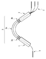
- FIG. 1 schematically shows a conventional arrayed waveguide grating type optical filter.
- the arrayed waveguide grating type optical filter is constituted by slab waveguides 1 and 2, an arrayed waveguide group 3, an input waveguide 4 and an output waveguide 5.
- the connection point with the slab waveguides 1 and 2 is an input of the slab waveguides 1 and 2.
- the arrayed waveguide group 3 is formed by sequentially connecting the straight waveguides 3a, the arc waveguides 3c, and the straight waveguides 3b.
- the convex direction of the arc of the arc waveguide 3c is only one direction in the case of FIG. 1 and only upward in the case of FIG.
- the waveguide of the if the lengths of the straight waveguide 3a and the straight waveguide 3b and the radius of the arc waveguide 3c are properly selected, all adjacent waveguides are different in length by a certain amount (d 0 )
- the arrayed waveguide group 3 can be arranged.
- the difference (d 0 ) in the length of adjacent waveguides of the arrayed waveguide group 3 is the parameter ( ⁇ 0 : central wavelength, n g : group refractive index, FSR) of the arrayed waveguide grating type optical filter. : Free spectral range) and the following equation (1).
- d 0 is referred to as a waveguide length difference
- d 0 ⁇ n e obtained by multiplying the effective refractive index n e of the waveguide is referred to as an optical path length difference.
- Wavelength interval ⁇ maximum number of channels ⁇ 0 2 / (d 0 ⁇ n g ) FSR (1)
- the waveguide length difference d 0 needs to be set short, but when the waveguide length difference d 0 is extremely short, in the arrayed waveguide group 3 described above The upper waveguide and the lower waveguide contact or intersect, which makes it difficult to operate the arrayed waveguide grating optical filter properly. That is, in the first prior art, there is a lower limit to the waveguide length difference that can be set due to geometrical limitations, so in the design method according to the first prior art setting the optical path length difference extremely short is geometrically Even if it can not be found or realized, the size of the circuit may become abnormally large.
- Patent Document 1 discloses an arrayed waveguide grating type filter configured of an S-shaped optical waveguide which is a second conventional example.
- FIG. 2 schematically shows an arrayed waveguide grating type optical filter according to a second prior art.
- the arrayed waveguide grating type optical filter is composed of slab waveguides 1 and 2, an arrayed waveguide group 3, and a fan-shaped arc waveguide group 6.
- the slab waveguides 1 and 2 are connected by an S-shaped array waveguide group 3, and the entire circuit configuration is substantially point-symmetrical.
- this S-shaped optical waveguide the directions of the arcs of the left arc waveguide 3c and the right arc waveguide 3d are opposite to each other. Therefore, when the arc waveguide group 6 is omitted and the arc waveguide 3c and the arc waveguide 3d are directly connected, the waveguide lengths can be designed to be generally equal. That is, the S-shaped optical waveguide is configured to temporarily cancel the waveguide length difference required for geometrical arrangement at the inflection point, and to be zero (0).
- the optical path length difference necessary for the filter operation is given by the fan-shaped arc waveguide group 6 inserted at the inflection point of the S-shaped optical waveguide.
- the fan-shaped circular waveguide group 6 is composed of circular waveguides having the same center point, the same opening angle, the constant interval, and the radius increased by a fixed amount. Since the optical path length difference of this circuit is determined by the waveguide difference (radius difference ⁇ opening angle) between the waveguides of the fan-shaped circular waveguide group 6, the wide FSR, that is, the optical path length difference is extremely short, The desired circuit can be designed.
- FIG. 3 is a schematic view of an arrayed waveguide grating type optical filter according to a third prior art.
- a third prior art example is an arrayed waveguide grating type filter composed of waveguides that are substantially line symmetric (see Patent Document 2).
- the arrayed waveguide grating type optical filter includes slab waveguides 1 and 2, arrayed waveguide group 3, input waveguide 4 and output waveguide 5, and fan-shaped circular waveguide group 6. Is equipped.
- the left portion of the arrayed waveguide group 3 is composed of an arrayed waveguide group 3g formed by sequentially connecting the straight waveguide 3a, the arc waveguide 3c, and the respective waveguides of the straight waveguide 3e.
- the portion on the right side among 3 is composed of an arrayed waveguide group 3h formed by sequentially connecting the linear waveguide 3f, the circular waveguide 3d, and the linear waveguide 3b.
- the difference in length between the adjacent upper waveguide and the lower waveguide is the same as in the first conventional example design method described with reference to FIG.
- the length of each linear waveguide and the radius of each circular waveguide it is possible to design constant.
- the convex directions of the arcs of the arc waveguide 3c and the arc waveguide 3d are all upward, the upper waveguide is necessarily longer than the lower waveguide. That is, the waveguide length difference can not be made zero only by the arrayed waveguide group 3g and the arrayed waveguide group 3h in which the convex directions of the arcs are equal.
- the degree of freedom of combination of arc waveguides is different as compared with the design method according to the second prior art described with FIG. Therefore, it may be possible to design an AWG with a smaller circuit size.
- Patent No. 2693354 Patent No. 3222810
- Non-Patent Document 3 the external dimensions of the module discussed as CFP 4 are extremely small, about 9.5 ⁇ 21.7 ⁇ 88 mm (CFP: an abbreviation for 100 G Form-factor Pluggable. C represents 100 in Roman numerals).
- CFP an abbreviation for 100 G Form-factor Pluggable.
- C represents 100 in Roman numerals.
- ROSA and TOSA must be arranged in parallel in a module of this size, and further electronic circuits etc. required for the transceiver must be arranged in series, this is acceptable for ROSA alone and also for the optical filter incorporated in ROSA. Space is extremely small.
- the output fanout portion for coupling to individual PDs is The size is strongly dependent also on the PD interval (or the terminal interval of TIA connected to PD), and there is a problem that sufficient miniaturization can not be achieved only by increasing ⁇ .
- the specifications recommended by the IEEE include not only the channel spacing of the optical wavelength but also the wavelength bandwidth in each channel. Therefore, it is necessary to secure the transmission wavelength bandwidth of the optical filter.
- the transmission wavelength bandwidth is expanded when the output waveguide is a multimode waveguide (Non-patent Document 4)
- the minimum bending radius of the multimode waveguide is larger than that of a single mode waveguide. Therefore, in the AWG according to the conventional design method, there is a problem that the size of the output fanout portion (expanded portion) also takes a large space in the circuit layout.
- optical transceivers for Ethernet are often used for connections within data centers and between data centers, optical transceivers for Ethernet are far superior to optical transceivers for telecommunications because they compete with inexpensive transceivers for electrical signals. Cost reduction is needed.
- the optical filter used for ROSA needs to be optically coupled on the input side via an optical cable connector and an optical component called a receptacle, and on the output side is optically coupled to four PDs via an optical lens.
- the simplest method of alignment is to insert the light of the signal light wavelength to be actually used from the above-mentioned optical cable, pass through the member for receptacle, the optical filter, the optical lens, and PD in order, and then the electrical output from the PD It is a method of mass-centering all parts at once while monitoring.
- this method requires a very complex multi-body aligning device, and there is a problem that the cost becomes extremely large.
- the PD, the optical filter, and the optical fiber that are optically connected to each other must be selected from different materials that have large differences in refractive index, reflection occurs at material boundaries. Furthermore, when a lens system is used to increase the coupling efficiency of each light coupling, an additional air layer is generated due to the air layer entering on each lens surface. In order to improve the reception S / N, it is general to apply an anti-reflection film for telecom applications, but for Ethernet applications, there is a problem that it is desired to avoid an increase in cost associated with an increase in the number of processes.
- the present invention has been made in view of the above-mentioned conventional problems, and it is possible to function as an extremely small AWG type optical filter which can constitute a small and inexpensive ROSA module necessary for realizing a high-speed Ethernet transceiver.
- the purpose is to provide a waver.
- Another object is to suppress the manufacturing cost of the ROSA module due to the circuit and chip shape added to the AWG type optical filter.
- the invention described in the embodiment comprises at least one input waveguide having an input at one end, and a first slab waveguide having one end connected to the other end of the input waveguide.
- a group of arrayed waveguides comprising a waveguide and a plurality of waveguides connected at one end to the other end of the first slab waveguide, and a second slab connected at one end to the other end of the arrayed waveguide group A waveguide, and at least one output waveguide connected at one end to the other end of the second slab waveguide and having an output at the other end, each waveguide of the arrayed waveguide group being conducted It has a first curved portion in which the extension direction of the waveguide changes by 180 degrees or more and a second curved portion in which the extension direction of the waveguide changes by 180 degrees or more in the opposite direction to the first curved portion. It is an optical multiplexer / demultiplexer to be
- FIG. 7 is a waveguide layout diagram of an arrayed waveguide grating type optical filter for CWDM signal four-channel demultiplexing designed in the first embodiment.
- FIG. 16 is a waveguide layout diagram of an arrayed waveguide grating type optical filter for CWDM signal four-channel demultiplexing designed in the second conventional example.
- FIG. 18 is a waveguide layout diagram of an arrayed waveguide grating type optical filter for four channels of CWDM signals designed in the third prior art example.
- FIG. 7 is a waveguide layout diagram of an arrayed waveguide grating type optical filter for LAN-WDM signal demultiplexing with aligned waveguides designed in a second embodiment. The first step in the process of aligning the input side member (receptacle) and the output side member (PD array etc.) to the arrayed waveguide grating optical filter with aligned waveguide designed in the second embodiment will be described It is a figure to do.
- the second step in the operation of aligning the input side member (receptacle) and the output side member (PD array etc.) to the arrayed waveguide grating type optical filter with aligned waveguide designed in the second embodiment It is a figure to do.
- the third step in the work of aligning the input side member (receptacle) and the output side member (PD array etc.) in the arrayed waveguide grating type optical filter with aligned waveguide designed in the second embodiment will be explained It is a figure to do.
- the optical multiplexer / demultiplexer comprises at least one input waveguide, a first slab waveguide connected to the input waveguide, and a plurality of parallel waveguides connected to the first slab waveguide.
- Array waveguide grating type comprising an arrayed waveguide group, a second slab waveguide connected to the arrayed waveguide group, and at least one output waveguide connected to the second slab waveguide.
- each waveguide of the arrayed waveguides connected to the first slab changes the extension direction of each waveguide by 180 degrees or more, and then the extension direction of the waveguides in the opposite direction is 180 degrees It is equipped with the structure connected to the 2nd slab in the latter part which changed as mentioned above.
- the “stretching direction of the waveguide” can be said to be equal to the optical axis direction of light guided in the waveguide.
- the arrayed waveguide group has the following configurations (1) to (3).
- Each waveguide of the arrayed waveguide group comprises a first portion and a second portion, and the first portion is formed from the output end of the input slab waveguide (first slab waveguide) Up to the connection point of the second portion, the optical path is bent 180 degrees or more in the first direction from the emission end, and the second portion is connected to the output slab waveguide from the connection point of the first portion Up to the incident end of (the second slab waveguide), the optical path is bent from the connection point in a second direction opposite to the first direction by 180 degrees or more.
- the “curved” optical path does not necessarily mean that all parts of the optical path are bent, and also includes an aspect having a portion where the curvature of the optical path is zero.
- Each waveguide of the arrayed waveguide group includes a first portion and a second portion, and the first portion is a connection point of the output end of the input slab waveguide to the second portion Up to an arc waveguide curved in a first direction by 180 degrees or more, and the second portion is opposite to the first direction from the connection point of the first portion to the incident end of the output slab waveguide And an arc waveguide curved at least 180 degrees in the second direction of
- the “arc waveguide” does not necessarily mean that all parts of the waveguide are bent, and also includes an aspect having a part where the waveguide has a curvature of 0.
- Each waveguide of the arrayed waveguide group includes a first arc waveguide and a second arc waveguide, and the first arc waveguide is a first waveguide from the output end of the input slab waveguide.
- the second arc waveguide is connected to the second arc waveguide, and the second arc waveguide is connected to the first arc waveguide at a point opposite to the first direction from the connection point with the first arc waveguide. Curved by 180 degrees or more in the direction 2 and connected to the input end of the output slab waveguide.
- Each arrayed waveguide connected to the first slab waveguide is connected to the second slab after the extension direction of the waveguide is once changed by 180 degrees or more and further changed by 180 degrees or more in the opposite direction.
- connection point between the input waveguide and the first slab waveguide and the second slab inside the right end and the left end of the region where the arrayed waveguide group consisting of a plurality of waveguides arranged in parallel is disposed.
- the input waveguide and the first waveguide are disposed inward from the uppermost end and the lowermost end of a region in which the connection point between the waveguide and the output waveguide is arranged and the arrayed waveguide group consisting of a plurality of parallel waveguides is arranged.
- the connection point with the slab waveguide and the connection point with the second slab waveguide and the output waveguide are arranged.
- the aligning input waveguide reaching a third side different from the first side of the optical multiplexer / demultiplexer to which the input waveguide reaches and the second side to which at least one of the output waveguides reaches And an input waveguide for alignment is connected to the first slab waveguide, and one end of the plurality of output waveguides not connected to the second slab waveguide is connected to each other It is looped by being done.
- One end of the alignment input waveguide is connected to one slab waveguide, and a loop waveguide is disposed in the other slab waveguide.
- At least one or more of the input waveguides or the output waveguides or the alignment input waveguides reach the chip side with an inclination of 8 degrees or more from the perpendicular to the chip side.
- FIG. 4 schematically shows an arrayed waveguide grating type optical filter according to this embodiment.
- the arrayed waveguide grating type optical filter according to this embodiment includes a first slab waveguide 11, a second slab waveguide 12, an arrayed waveguide group 13, and an input waveguide 14. And an output waveguide 15.
- the arrayed waveguide group 13 includes a straight waveguide 13a, an arc waveguide 13b, an arc waveguide 13c, a straight waveguide 13d, an arc waveguide 13e, an arc waveguide 13f, and a first waveguide length difference.
- An arrayed waveguide group consisting of S-shaped waveguides formed by connecting the waveguides 13 k in tandem, and the total length of each S-shaped waveguide monotonously increases or decreases monotonously by a fixed value between adjacent waveguides. ing.
- the length of each waveguide of the waveguides 17b may be zero, respectively.
- Each of the S-shaped waveguides constituting the arrayed waveguide group 13 is orthogonal to the first reference line 18a from the first slab waveguide 11 through the linear waveguide 13a and the circular waveguide 13b, and the circular waveguide 13c and the straight waveguide 13d to be orthogonal to the second reference line 18b, to pass through the arc waveguide 13e to be orthogonal to the third reference line 18c, and to pass through the arc waveguide 13f to be orthogonal to the fourth reference line 18d
- the S-shaped waveguides constituting the arrayed waveguide group 13 form an arc waveguide 13c and an arc when the propagation direction of the optical signal is set from the first slab waveguide 11 to the second slab waveguide 12
- the waveguide 13e is convex to the right in the propagation direction
- the arc waveguide 13f, the arc waveguide 13g, and the arc waveguide 13i are convex to the left in the propagation direction.
- the sum of the opening angles of the arc waveguide 13c and the arc waveguide 13e and the sum of the opening angles of the arc waveguide 13f, the arc waveguide 13g, and the arc waveguide 13i are designed to be the same value. For this reason, the lengths of the S-shaped waveguides become approximately equal except for the first linear waveguide 17a for adjusting the length difference of the first waveguide and the second linear waveguide 17b for adjusting the length difference of the second waveguide.
- the lengths of the linear waveguide 13 d and the linear waveguide 13 h are also different for each S-shaped waveguide. The difference in these lengths is due to the extension of the straight waveguide 13a crossing at the first reference point 19a and the extension of the straight waveguide 13k crossing at the second reference point 19b.
- the opening angle 20a of the straight waveguide 13a centered on the first reference point 19a and the opening angle 20b of the straight waveguide 13k centered on the second reference point 19b are the input waveguide 11 and the output waveguide 14
- the design gives values similar to the numerical aperture of.
- the difference in total extension of the S-shaped waveguides adjacent to each other is within a few ⁇ m.
- that amount is used to adjust the length of the first linear waveguide 17a for adjusting the waveguide length difference and the second waveguide length difference.
- the total length of each S-shaped waveguide can be designed to be exactly zero by adjusting the length of the linear waveguide 17b of
- the arrayed waveguide group 13 includes a first curved portion formed of waveguides from the first reference line 18a to the fifth reference line 18c, and a guide line 5c from the fifth reference line 18c to the second reference line 18f. And a second curved portion formed of a waveguide.
- the first curved portion is a portion where waveguides constituting the arrayed waveguide group 13 are bent 180 degrees or more.
- the second curved portion is a portion where the waveguides constituting the arrayed waveguide group 13 are bent 180 degrees or more in the opposite direction to the first curved portion.
- the optical axis direction of the light guided in the arrayed waveguide group 13 changes by 180 degrees or more between the first reference line 18a and the fifth reference line 18c, and the fifth reference line 18c to the fifth reference line 18c Between the two reference lines 18f, the angle changes by 180 degrees or more in the opposite direction to the first curved portion.
- the waveguide length difference d 0 is calculated using the above-mentioned equation (1) Of the length of the first straight waveguide 17a for adjusting the length difference of the first waveguide and the second length adjustment of the second waveguide so that the difference between the adjacent S-shaped waveguides becomes equal to the difference of the total extension.
- the length of the linear waveguide 17b may be designed.
- Wavelength interval ⁇ maximum number of channels ⁇ 0 2 / (d 0 ⁇ n g ) FSR equation (1)
- ⁇ 0 is a central wavelength
- n g is a group refractive index
- FSR is a free spectral range.
- FIG. 5 is a waveguide layout diagram of an arrayed waveguide grating type optical filter for CWDM signal 4-channel demultiplexing actually designed by the above-mentioned design method.
- the waveguide used is a buried waveguide in which germanium is added to silica glass, the relative refractive index difference is 2%, the core height of the standard waveguide is 4 ⁇ m, and the core width is 4 ⁇ m.
- the minimum bending radius in the 1300 nm band was 750 ⁇ m described above.
- the wavelengths of the demultiplexed optical signals are set to 1271 nm, 1291 nm, 1311 nm, and 1331 nm, and the FSR is set to 3250 GHz in order to reduce the difference in transmission loss between channels.
- the waveguide length difference given between adjacent S-shaped array waveguides was 6.498 ⁇ m.
- the waveguide widths of the input waveguide 14 and the output waveguide 15 are made different values. Specifically, the width of the input waveguide 14 connected to the first slab waveguide 11 is 8.0 ⁇ m, and the width of the four output waveguides 15 connected to the second slab waveguide 12 is 15 ⁇ m. did.
- the minimum bending radius is set to 1200 ⁇ m because high-order mode light is also propagated to the output waveguide 15 having a width of 15 ⁇ m. Since the distance between the light receiving surfaces of the four PD arrays prepared was 250 ⁇ m, the distance between the output waveguides was 250 ⁇ m.
- connection point between the second slab waveguide 12 and the output waveguide 15 is set to the array waveguide group 13. Were placed inside the right end and the left end of the area to be placed and inside the top end and the lowest end. That is, the connection point between the second slab waveguide 12 and the output waveguide 15 is taken from the chip side on which the waveguide is formed (indicated by a rectangular frame surrounding the waveguide in FIG. 5) from the arrayed waveguide group 13 The distance from the chip side to the second slab waveguide 12 is larger than the distance to the distance.
- connection point between the first slab waveguide 11 and the input waveguide 14 is located at the inside of the right end and the left end of the region where the arrayed waveguide group 13 is disposed and the uppermost end. It was arranged to be inside the lower end. That is, the first slab waveguide from the chip side is closer to the connection point between the first slab waveguide 11 and the output waveguide 14 than the distance from the chip side where the waveguide is formed to the arrayed waveguide group 13. It arranges so that the distance to reach 11 becomes large.
- the specific arrangement of the arrayed waveguide group 13 was designed according to the design method described using FIG.
- the chip side is designed to reach the chip side with an inclination of 8 degrees from the vertical with respect to the chip side on the output side.
- the chip side may be reached with an inclination of 8 degrees similarly to the chip side on the input side.
- the chip size is as small as 8.2 mm in length and 4.9 mm in width. I was able to fit the AWG in my footprint.
- connection point between the second slab waveguide 12 and the output waveguide 15 is located inside the right end and the left end of the region where the arrayed waveguide group 13 is disposed and inside the top end and the lowest end.
- arranging the position of the output waveguide 15 at the chip end in the center of the chip is obtained as a secondary effect. If the position of the output waveguide 15 at the chip end can be made to be at the center of the chip, useless expansion space in the vertical direction is eliminated when mounting PDs and TIAs and extraction electrodes, so the module size of ROSA is finally reduced. It has the merit of being able to
- FIG. 6 is a result of layout calculation of the arrayed waveguide grating type optical multiplexer / demultiplexer having the same wavelength arrangement, for comparison, with the same waveguide structure by the design method of the second conventional example.
- the arrayed waveguide group 13 of the arrayed waveguide grating type optical multiplexer / demultiplexer shown in FIG. 6 is composed of S-shaped optical waveguides running in parallel, and has a substantially point-symmetrical structure as a whole.
- the finished chip size was 11.8 mm long and 3.9 mm wide.
- the chip width of 3.9 mm is narrower than the arrayed waveguide grating type optical multiplexer / demultiplexer shown in FIG.
- the chip width is larger than that of the arrayed waveguide grating type optical multiplexer / demultiplexer according to the design method of the present invention.
- the chip length of 11.8 mm is longer by about 44 mm than the arrayed waveguide grating type optical multiplexer / demultiplexer shown in FIG. 5 according to the design method of the present invention by about 44%.
- FIG. 7 is a result of layout calculation of an arrayed waveguide grating type optical multiplexer / demultiplexer having the same wavelength arrangement in the same waveguide structure by the design method of the third conventional example for comparison.
- the arrayed waveguide group 13 of the arrayed waveguide grating type optical multiplexer / demultiplexer shown in FIG. 7 has a substantially linearly symmetrical structure as a whole. In the central portion and both side portions of the arrayed waveguide group 13, the direction in which the arcs of the arc waveguides become convex is opposite to each other.
- the finished chip size was 14.3 mm long and 3.1 mm wide.
- the chip width could be as narrow as 4.1 mm even with the additional restriction of centering the position of the output waveguide 15 on the chip side.
- the chip length 14.3 mm is 6.1 mm longer than the arrayed waveguide grating type optical multiplexer / demultiplexer shown in FIG. 5 according to the design method of the present invention by about 75%.
- An arrayed waveguide grating type optical multiplexer / demultiplexer according to the design method of the present invention shown in FIG. 5 an arrayed waveguide grating type optical multiplexer / demultiplexer according to the design method of the second conventional example shown in FIG.
- Array waveguide grating type optical multiplexer / demultiplexer according to the third prior art design method The chip area of each is about 40 square mm, about 46 square, excluding the restriction that the position of the output waveguide is at the center of the chip mm, about 44 square mm.
- the chip price is estimated from the yield per wafer, it is about 15% as compared with the first conventional optical multiplexer / demultiplexer by using the arrayed waveguide grating type multiplexer / demultiplexer according to the design method of the present invention. It has been found that the chip cost can be reduced by about 10% as compared with the second conventional optical multiplexer / demultiplexer.
- the waveguides of the arrayed waveguide group change the extension direction by 180 degrees or more in the reverse direction after the extension direction is once changed by 180 degrees or more. Furthermore, the first slab waveguide and the second slab waveguide are disposed at the innermost end of the rightmost end and the leftmost end of the region where the arrayed waveguide group is disposed and the innermost end of the uppermost end and the lowermost end. As a result, a small chip size is realized.
- the extension direction of the waveguide is changed by 180 degrees or more, and miniaturization is realized with low loss.
- This is realized by using a waveguide that can endure sharper bending as compared to a normal silica glass waveguide (with a relative refractive index difference of 1% or less).
- the minimum bending radius which can bend the waveguide is 2 mm or more. If it is sharply bent more than that, the transmitted light is not completely bent in the normal silica glass waveguide, and is emitted out of the waveguide as emitted light. Therefore, if a normal waveguide is used for sharp bending, the loss of the arrayed waveguide multiplexer / demultiplexer increases.
- the minimum bending radius in a wavelength of 1300 nm band
- the minimum bending radius can be sharply bent to 750 ⁇ m or less than that of a normal waveguide.
- a low-loss arrayed waveguide multiplexer / demultiplexer is realized in a small configuration by changing the extension direction of the waveguide by 180 degrees or more. ing.
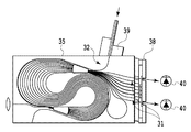
- FIG. 8 is a waveguide layout diagram of an arrayed waveguide grating type optical filter for LAN-WDM signal demultiplexing with a waveguide for alignment designed in this embodiment.
- the material and waveguide parameters of the waveguide used are the same as those of the arrayed waveguide grating type optical multiplexer / demultiplexer shown in FIG. 5, but the wavelength of the optical signal to be branched is different.
- the wavelengths of the four waves are 1295.56 nm, 130.05 nm, 1304.58 nm, and 1309.14 nm, and the FSR is set to 7830 GHz in consideration of the interchannel difference in transmission loss.
- the waveguide length difference given between adjacent S-shaped array waveguides was 25.79 ⁇ m.
- the waveguides of the input waveguide 14 and the output waveguide 15 are shown in order to make the flatness in the transmission region of the multiplexing / dividing characteristics appear. I made the width different. Specifically, the width of the input waveguide 14 connected to the first slab waveguide 11 is 8.0 ⁇ m, and the width of the four output waveguides 15 connected to the second slab waveguide 12 is 15 ⁇ m. did.
- the minimum bending radius of the output waveguide with a width of 15 ⁇ m is 1200 ⁇ m, and the distance between the output waveguides 15 at the chip side is 250 ⁇ m.
- the first slab waveguide 11 and the input waveguide 14 are connected similarly to the arrayed waveguide grating type optical multiplexer / demultiplexer shown in FIG.
- the connection point and the connection point between the second slab waveguide 12 and the output waveguide 15 are the inside of the right end and the left end of the region where the arrayed waveguide group 13 is disposed and the inside of the top end and the lower end. Arranged to be.
- the first alignment alignment consisting of a single mode waveguide for aligning the optical lens array on both sides of the output waveguide 15 consisting of four multimode waveguides shown in FIG.
- the optical input waveguide 32 for alignment is disposed on the upper side of the chip.
- the aligning light input waveguide 32 is connected to the first slab waveguide 11 to which the input waveguide 14 of the arrayed waveguide grating type optical multiplexer / demultiplexer is connected.
- the second slab waveguide 12 to which the output waveguide 15 of the arrayed waveguide grating type optical multiplexer / demultiplexer is connected has a loop-like guiding so that the optical signal input from the optical input waveguide 32 for alignment can be folded back.
- the waveguide 33 was connected.
- a third alignment light output waveguide 34 for alignment which is output to the lower side of the chip, is disposed beside the loop waveguide 33.
- the output waveguide 15 disposed on the right side of the chip, one pair (two) 30 of the first alignment light output waveguides, and the second alignment light output The angle which each waveguide of one set (two) 31 of waveguides makes with the chip right side was set to 8 degrees.
- the angle of the aligning light input waveguide 32 to the upper side of the chip and the angle of the third aligning light output waveguide 34 to the lower side of the chip are set to 8 degrees.
- the AR (Anti-Reflection) coating for suppressing the reflection amount in the 1.3 band is applied to the end face of the right side of the chip, the angle formed by the input waveguide 14 with the left side of the chip is vertical here.
- the wavelength of 1324.2 nm from the third alignment light output waveguide 34 on the lower side of the chip Light is output, and light of wavelength of 1287.8 nm and 1308.0 nm is often output from the first set of light output waveguides for alignment of light lenses and arrays, and PD array alignment is performed.
- Light of wavelength of 1285.6 nm and 1310.28 nm is outputted from one set 31 of the second optical output waveguides for alignment, and an arrayed waveguide grating type optical filter in which members for receptacle are aligned and installed
- the light having a wavelength of 1319.5 nm is output to the input waveguide 14 of Note that light is output to the input waveguide 14 through the following route.
- light with a wavelength of 1319.5 nm passes through the first slab waveguide 11 and the second slab waveguide 12 and passes through the loop waveguide 33 again.
- the light is input to the second slab waveguide 12 and output from the first slab waveguide 11 to the input waveguide 14.
- 9A, 9B, 9C, and 9D show an arrayed waveguide grating type optical filter chip 35 for LAN-WDM signal demultiplexing with a waveguide for alignment shown in FIG. It is the schematic which showed the process of mounting the member 37 which accumulated the array, and the member 38 for receptacles.
- a single core optical fiber The block 39 is temporarily fixed (FIG. 9A). More specifically, the outgoing light of the third optical output waveguide 34 for centering on the lower side of the optical filter chip 35 is received using the large aperture PD 36, and the optical filter chip 35 and a single core optical fiber block After performing two-piece alignment with 39, temporary fixation is performed. In the temporary fixing, after the assembly process, the single-core optical fiber block 39 can be removed using an adhesive with weak adhesion or bonding conditions. In addition, since the end face of the one-core optical fiber block 39 used here is polished at 8 degrees, it is possible to perform optical coupling while suppressing the loss and reflection at the upper side of the chip to a small value.
- the fourth step when light having wavelengths of 1285.6 nm and 1310.28 nm is input to the optical input waveguide 32 for centering on the upper side of the chip through the temporarily fixed one-core optical fiber block 39, the second Light is output from the alignment light output waveguide 31.
- the output light is used to align the member 38 in which the PD array is accumulated with a two-body aligning device, and after the alignment is completed, adhesive fixation is performed. (FIG. 9D)
- the light from the light input waveguide for alignment is connected to the first slab waveguide at the third chip side different from the input and output, and the loop waveguide is connected to the second slab waveguide.
- the loop waveguide is connected to the second slab waveguide.
- GRIN GRadient INdex
- AR Anti Reflection
- FIGS. 9A, 9B, 9C, and 9D eight GRIN (GRadient INdex) lenses are aligned and fixed as the light lens array 36, and then the end face is polished at 8 degrees. The thing was used. Of the both end faces of the light lens array 36, AR (Anti Reflection) coating is applied on the PD array side, but AR coating is omitted on the light filter chip 35 side, and only polishing is performed. Also, in the arrayed waveguide grating type optical multiplexer / demultiplexer according to the present invention shown in FIGS.
- the AR coating is omitted on the end face on which the light lens array 36 is mounted, and only polishing is performed. Further, for bonding between the light filter chip 35 and the light lens array 36, an adhesive whose refractive index after curing substantially matches that of quartz glass was used.
- the AR coat was omitted in the chip upper side with the end of the alignment input waveguide 32 used during alignment and the chip underside with the end of the alignment input waveguide 34, and polishing was performed only.
- the amount of return loss measured from the boundary between the light filter chip 35 and the light lens array 36 mounted in this manner was 40 dB or more. That is, if the arrayed waveguide grating type optical multiplexer / demultiplexer according to the present invention is used, it becomes possible to eliminate the execution of AR coating, which causes the cost increase, by increasing the number of processes up to four times. As a result, it is possible to provide a cheaper ROSA.
- the above effect can be obtained similarly between the optical filter chip 35 and the receptacle member 37.
- FIG. 10 shows the mounting described with FIG. 9A, FIG. 9B, FIG. 9C and FIG. 9D to an arrayed waveguide grating type optical filter for LAN-WDM signal demultiplexing with a waveguide for alignment described with reference to FIG. It is a figure which shows the wavelength dependency of the light reception sensitivity of the ROSA module which mounted the member 37 for receptacles, the optical lens array 36, and the member 38 which integrated the PD array by the method.
- the size of the optical filter chip 35 is small with a length of 8.2 mm and a width of 4.9 mm, it can be seen that it satisfies sufficient demultiplexing characteristics.
- optical multiplexer / demultiplexer used as ROSA was mentioned as the example and demonstrated, it is not limited to this, The optical multiplexer / demultiplexer can also be used as TOSA from the symmetry of light.
Landscapes
- Physics & Mathematics (AREA)
- Engineering & Computer Science (AREA)
- Microelectronics & Electronic Packaging (AREA)
- General Physics & Mathematics (AREA)
- Optics & Photonics (AREA)
- Computer Networks & Wireless Communication (AREA)
- Signal Processing (AREA)
- Electromagnetism (AREA)
- Optical Integrated Circuits (AREA)
Abstract
Description
図4は本実施例にかかるアレイ導波路格子型光フィルタの概略を示す。本実施例にかかるアレイ導波路格子型光フィルタは、図4に示すように、第1のスラブ導波路11と、第2のスラブ導波路12と、アレイ導波路群13と、入力導波路14と、出力導波路15とを備えている。
ここで、比屈折率差2%以上の導波路を用いると最小曲げ半径は(波長1300nm帯において)750μm以下と通常の導波路より急峻に曲げられるようになる。
本実施例では、調心用導波路付きLAN-WDM信号分波用アレイ導波路格子型光フィルタとして機能させるために、実施例1のアレイ導波路格子型光合分波器を、分波する光信号の波長が異なる構成としている。図8は、本実施例で設計した調心用導波路付きLAN-WDM信号分波用アレイ導波路格子型光フィルタの導波路配置図である。用いた導波路の材質と導波路パラメータは、図5に示したアレイ導波路格子型光合分波器と同一であるが、分波する光信号の波長が異なる。4波の波長を1295.56nm、1300.05nm、1304.58nm、1309.14nmとし、透過損失のチャネル間格差を考慮しFSRを7830GHzとした。結果、隣接するS字状アレイ導波路間に付与する導波路長差は、25.79μmとした。また、図5に示したアレイ導波路格子型光合分波器と同様に、合分波特性の透過域での平坦性を出現させるため、入力導波路14と出力導波路15との導波路幅を違う値にした。具体的には第1のスラブ導波路11に接続される入力導波路14の幅を8.0μmとし、第2のスラブ導波路12に接続される4本の出力導波路15の幅を15μmとした。
2 第2のスラブ導波路
3 アレイ導波路群
3a、3b、3e、3f 直線導波路
3c、3d 円弧導波路
4 入力導波路
5 出力導波路
6 扇型円弧導波路群
11 第1のスラブ導波路
12 第2のスラブ導波路
13 アレイ導波路群
13a、13d、13h、13k 直線導波路
13b、13c、13e、13f、13g、13i、13j 円弧導波路
14 入力導波路
15 出力導波路
17 導波路長差調整用の直線導波路群
17a 第1の導波路長差調整用の直線導波路
17b 第2の導波路長差調整用の直線導波路
18a 第1の基準線
18b 第2の基準線
18c 第3の基準線
18d 第4の基準線
18e 第5の基準線
18f 第6の基準線
19a 第1の基準点
19b 第2の基準点
20a 第1の基準点19aを中心とする直線導波路13aの開き角
21a 第2の基準点19bを中心とする直線導波路13bの開き角
22 出力導波路のファインアウト部分
30 第1の調心用光出力導波路
31 第2の調心用光出力導波路
32 調心用光入力導波路
33 ループ状導波路
34 第3の調心用光出力導波路
35 光フィルタ・チップ
36 光レンズ・アレイ
37 PDアレイを集積した部材
38 レセプタクル用部材
39 1芯の光ファイバ・ブロック
40 大口径PD
Claims (6)
- 一端に入力部を有する少なくとも1本の入力導波路と、
一端が前記入力導波路の他端に接続された第1のスラブ導波路と、
一端が前記のスラブ導波路の他端に接続された複数本の導波路を有するアレイ導波路群と、
一端が前記アレイ導波路群の他端に接続された第2のスラブ導波路と、
一端が前記第2のスラブ導波路の他端に接続され、他端に出力部を有する少なくとも1本の出力導波路とを備え、
前記アレイ導波路群の各導波路は、導波路の延伸方向が180度以上変化する第1の曲部と、該第1の曲部とは逆方向に導波路の延伸方向が180度以上変化する第2の曲部とを有することを特徴とする光合分波器。 - 前記入力導波路の入力部と前記出力導波路の出力部とは前記光合分波器の対向する端部にそれぞれ設けられ、
前記入力導波路と前記第1のスラブ導波路との接続点と、前記第2のスラブ導波路と出力導波路と前記の接続点とは、前記アレイ導波路群が配置された領域より内側に配置されていることを特徴とする請求項1に記載の光合分波器。 - 前記入力導波路の入力部と前記出力導波路の出力部とは前記光合分波器の対向する端部にそれぞれ設けられ、
一端が前記第1のスラブ導波路の他端に接続され、他端に入力部を有する調心用入力導波路をさらに備え、
前記調心用入力導波路の入力部は、前記入力導波路の入力部および前記出力導波路の出力部と同じ平面内であって、前記対向する端部とは異なる前記光合分波器の端部に設けられ、
前記出力導波路のうち2本の他端には出力部がなく、かつ互いに接続されていることにより、ループ状になっていることを特徴とする請求項1に記載の光合分波器。 - 前記光合分波器は、長方形の平板状のチップに形成され、前記入力導波路の入力部および前記出力導波路の出力部および前記調心用入力導波路のうち少なくとも一本以上の導波路がチップ辺に対して垂直より8度以上の傾きをなすことを特徴とする請求項1に記載の光合分波器。
- 前記光合分波器は、長方形の平板状のチップに形成され、前記入力導波路の入力部および前記出力導波路の出力部および前記調心用入力導波路のうち少なくとも一本以上の導波路がチップ辺に対して垂直より8度以上の傾きをなすことを特徴とする請求項2に記載の光合分波器。
- 前記光合分波器は、長方形の平板状のチップに形成され、前記入力導波路の入力部および前記出力導波路の出力部および前記調心用入力導波路のうち少なくとも一本以上の導波路がチップ辺に対して垂直より8度以上の傾きをなすことを特徴とする請求項3に記載の光合分波器。
Priority Applications (5)
| Application Number | Priority Date | Filing Date | Title |
|---|---|---|---|
| EP13837205.7A EP2896979B1 (en) | 2012-09-14 | 2013-09-13 | Optical multiplexer/demultiplexer |
| CA2884318A CA2884318C (en) | 2012-09-14 | 2013-09-13 | Optical multiplexer/demultiplexer |
| CN201380047618.7A CN104620147B (zh) | 2012-09-14 | 2013-09-13 | 光合波分波器 |
| JP2014535386A JP6016312B2 (ja) | 2012-09-14 | 2013-09-13 | 光合分波器 |
| US14/424,358 US9407371B2 (en) | 2012-09-14 | 2013-09-13 | Optical multiplexer/demultiplexer |
Applications Claiming Priority (2)
| Application Number | Priority Date | Filing Date | Title |
|---|---|---|---|
| JP2012203265 | 2012-09-14 | ||
| JP2012-203265 | 2012-09-14 |
Publications (1)
| Publication Number | Publication Date |
|---|---|
| WO2014041821A1 true WO2014041821A1 (ja) | 2014-03-20 |
Family
ID=50277961
Family Applications (1)
| Application Number | Title | Priority Date | Filing Date |
|---|---|---|---|
| PCT/JP2013/005463 Ceased WO2014041821A1 (ja) | 2012-09-14 | 2013-09-13 | 光合分波器 |
Country Status (6)
| Country | Link |
|---|---|
| US (1) | US9407371B2 (ja) |
| EP (1) | EP2896979B1 (ja) |
| JP (1) | JP6016312B2 (ja) |
| CN (1) | CN104620147B (ja) |
| CA (1) | CA2884318C (ja) |
| WO (1) | WO2014041821A1 (ja) |
Cited By (2)
| Publication number | Priority date | Publication date | Assignee | Title |
|---|---|---|---|---|
| US9729243B2 (en) | 2015-04-23 | 2017-08-08 | Centera Photonics Inc. | Optoelectronic transmitter, optoelectronic receiver and optoelectronic transceiver |
| WO2025177442A1 (ja) * | 2024-02-20 | 2025-08-28 | Ntt株式会社 | アレイ導波路回折格子 |
Families Citing this family (7)
| Publication number | Priority date | Publication date | Assignee | Title |
|---|---|---|---|---|
| US9401773B1 (en) * | 2015-03-04 | 2016-07-26 | Alliance Fiber Optic Products, Inc. | Compact multi-channel WDM devices for high-speed data communications |
| JP2017090575A (ja) * | 2015-11-05 | 2017-05-25 | 株式会社フジクラ | 光合分波素子及び光変調器 |
| KR101978913B1 (ko) * | 2015-11-16 | 2019-05-16 | 한국전자통신연구원 | 다채널 광 수신기 및 그의 제조 방법 |
| US9711930B2 (en) * | 2015-12-01 | 2017-07-18 | Seagate Technology Llc | Optical signal waveguide dispersion filter |
| WO2019095133A1 (en) * | 2017-11-15 | 2019-05-23 | Source Photonics (Chengdu) Company Limited | Waveguide array module and receiver optical sub-assembly |
| US10634844B1 (en) * | 2019-02-21 | 2020-04-28 | Applied Optoelectronics, Inc. | Optical multiplexer\demultiplexer with input and output ports on a single side, and an optical transceiver implementing same |
| CN110596813B (zh) * | 2019-08-02 | 2020-07-14 | 浙江大学 | 一种支持低损耗基模传输的硅基多模螺旋波导延迟线 |
Citations (3)
| Publication number | Priority date | Publication date | Assignee | Title |
|---|---|---|---|---|
| JP2693354B2 (ja) | 1992-04-10 | 1997-12-24 | エイ・ティ・アンド・ティ・コーポレーション | 光デバイス |
| JP3222810B2 (ja) | 1996-08-06 | 2001-10-29 | 日本電信電話株式会社 | アレイ導波路格子 |
| JP2011513779A (ja) * | 2008-02-28 | 2011-04-28 | シスパリエ グループ リミテッド ライアビリティー カンパニー | Cwdmに適した改良型導波路グレーティング光ルータ |
Family Cites Families (10)
| Publication number | Priority date | Publication date | Assignee | Title |
|---|---|---|---|---|
| JPH03222810A (ja) | 1990-01-26 | 1991-10-01 | Calsonic Corp | 車両の排気ガス導出装置 |
| DE69723626T2 (de) | 1996-08-06 | 2004-06-09 | Nippon Telegraph And Telephone Corp. | Wellenleiter-Matrix-Gitter |
| US6731828B2 (en) * | 2001-07-04 | 2004-05-04 | Nippon Telegraph And Telephone Corporation | Waveguide-type optical signal processing circuit |
| JP3962227B2 (ja) * | 2001-07-04 | 2007-08-22 | 日本電信電話株式会社 | 導波路型光信号処理回路 |
| JP3650348B2 (ja) * | 2001-08-13 | 2005-05-18 | 日本電信電話株式会社 | 周波数選択光フィルタ |
| JP2003090925A (ja) * | 2001-09-17 | 2003-03-28 | Fdk Corp | 光導波路デバイス |
| JP4263027B2 (ja) * | 2003-06-18 | 2009-05-13 | 日本電信電話株式会社 | 導波路型光信号処理器 |
| TWI258605B (en) * | 2004-12-22 | 2006-07-21 | Ind Tech Res Inst | Dynamic optical power equalizer |
| JP4365879B1 (ja) * | 2008-05-21 | 2009-11-18 | Nttエレクトロニクス株式会社 | 平面光波回路 |
| US8340484B2 (en) * | 2010-01-05 | 2012-12-25 | Board Of Regents, The University Of Texas System | Compact multi-port optical signal processor |
-
2013
- 2013-09-13 CN CN201380047618.7A patent/CN104620147B/zh active Active
- 2013-09-13 WO PCT/JP2013/005463 patent/WO2014041821A1/ja not_active Ceased
- 2013-09-13 JP JP2014535386A patent/JP6016312B2/ja active Active
- 2013-09-13 EP EP13837205.7A patent/EP2896979B1/en active Active
- 2013-09-13 US US14/424,358 patent/US9407371B2/en active Active
- 2013-09-13 CA CA2884318A patent/CA2884318C/en active Active
Patent Citations (3)
| Publication number | Priority date | Publication date | Assignee | Title |
|---|---|---|---|---|
| JP2693354B2 (ja) | 1992-04-10 | 1997-12-24 | エイ・ティ・アンド・ティ・コーポレーション | 光デバイス |
| JP3222810B2 (ja) | 1996-08-06 | 2001-10-29 | 日本電信電話株式会社 | アレイ導波路格子 |
| JP2011513779A (ja) * | 2008-02-28 | 2011-04-28 | シスパリエ グループ リミテッド ライアビリティー カンパニー | Cwdmに適した改良型導波路グレーティング光ルータ |
Non-Patent Citations (6)
| Title |
|---|
| "CFP Multi-Source Agreement", CFP MSA, Retrieved from the Internet <URL:http://www.cfp-msa.org/> |
| "IEEE Std 802.3ba-2010", IEEE STANDARDS BOARD MEETING, June 2010 (2010-06-01), Retrieved from the Internet <URL:http://www.ieee802.org/3/ba/> |
| JOURNAL OF LIGHTWAVE TECHNOLOGY, vol. 27, no. 6, 15 March 2009 (2009-03-15), pages 786 - 790, XP011255464 * |
| K. MOCHIZUKI ET AL.: "Built-in Optics for 4ch-WDM ROSA in 100Gbps Ethernet", OECC2010, 2010 |
| S. KAMEI ET AL.: "Low-loss and flat/wide-passband CWDM demultiplexer using silica-based AWG with multi-mode output waveguide", TUI2 OFC, 2004 |
| See also references of EP2896979A4 |
Cited By (2)
| Publication number | Priority date | Publication date | Assignee | Title |
|---|---|---|---|---|
| US9729243B2 (en) | 2015-04-23 | 2017-08-08 | Centera Photonics Inc. | Optoelectronic transmitter, optoelectronic receiver and optoelectronic transceiver |
| WO2025177442A1 (ja) * | 2024-02-20 | 2025-08-28 | Ntt株式会社 | アレイ導波路回折格子 |
Also Published As
| Publication number | Publication date |
|---|---|
| CN104620147B (zh) | 2018-01-19 |
| CN104620147A (zh) | 2015-05-13 |
| EP2896979A4 (en) | 2016-06-08 |
| EP2896979A1 (en) | 2015-07-22 |
| JP6016312B2 (ja) | 2016-10-26 |
| EP2896979B1 (en) | 2017-08-16 |
| JPWO2014041821A1 (ja) | 2016-08-18 |
| CA2884318A1 (en) | 2014-03-20 |
| US9407371B2 (en) | 2016-08-02 |
| CA2884318C (en) | 2017-02-14 |
| US20150229400A1 (en) | 2015-08-13 |
Similar Documents
| Publication | Publication Date | Title |
|---|---|---|
| JP6016312B2 (ja) | 光合分波器 | |
| US11646794B2 (en) | Fiber optic connectors and connectorized fiber optic cables that include integrated photonic optical mode field converters and related methods | |
| CN101720443A (zh) | 用于多路复用器波导耦合的方法和系统 | |
| CN110832367B (zh) | 与硅光子平台集成的自由空间cwdm mux/demux | |
| JP3784701B2 (ja) | 光回路部材および光トランシーバ | |
| JPH116928A (ja) | アレイ導波路格子型波長合分波器 | |
| US20190052362A1 (en) | Method And System For A Free Space CWDM MUX/DEMUX For Integration With A Grating Coupler Based Silicon Photonics Platform | |
| WO2013046696A1 (ja) | 光合流分岐器、双方向光伝播器、及び光送受信システム | |
| US11474299B2 (en) | Wavelength-division multiplexing devices with modified angles of incidence | |
| CN111263906A (zh) | 用于接近法向入射mux/demux设计的方法和系统 | |
| US20130287407A1 (en) | Hybrid Multichannel or WDM Integrated Transceiver | |
| CN110785686A (zh) | 用于与硅光子平台集成的自由空间cwdm mux/demux | |
| JP2014182213A (ja) | 光素子 | |
| JP5180118B2 (ja) | 光波長多重信号監視装置 | |
| JP2009093131A (ja) | アレイ型タップフォトダイオードモジュールおよびその製造方法 | |
| US12111504B2 (en) | Alignment method for optical waveguide element | |
| US20040086221A1 (en) | Low cost, hybrid integrated dense wavelength division multiplexer/demultiplexer for fiber optical networks | |
| CN114200588A (zh) | 一种光解复用组件结构和封装方法 | |
| US20240151916A1 (en) | Microscale multi-functional optical structure | |
| US12174422B2 (en) | Optical circuit | |
| WO2026042849A1 (ja) | 光回路 | |
| KR101992142B1 (ko) | 이종 서비스를 결합하기 위한 광모듈 | |
| KR20190001316A (ko) | 오버레이를 위한 광모듈 |
Legal Events
| Date | Code | Title | Description |
|---|---|---|---|
| 121 | Ep: the epo has been informed by wipo that ep was designated in this application |
Ref document number: 13837205 Country of ref document: EP Kind code of ref document: A1 |
|
| ENP | Entry into the national phase |
Ref document number: 2014535386 Country of ref document: JP Kind code of ref document: A |
|
| WWE | Wipo information: entry into national phase |
Ref document number: 14424358 Country of ref document: US |
|
| REEP | Request for entry into the european phase |
Ref document number: 2013837205 Country of ref document: EP |
|
| ENP | Entry into the national phase |
Ref document number: 2884318 Country of ref document: CA |
|
| NENP | Non-entry into the national phase |
Ref country code: DE |