WO2014050245A1 - 静電容量型センサシート、静電容量型センサシートの製造方法及びセンサ - Google Patents
静電容量型センサシート、静電容量型センサシートの製造方法及びセンサ Download PDFInfo
- Publication number
- WO2014050245A1 WO2014050245A1 PCT/JP2013/068143 JP2013068143W WO2014050245A1 WO 2014050245 A1 WO2014050245 A1 WO 2014050245A1 JP 2013068143 W JP2013068143 W JP 2013068143W WO 2014050245 A1 WO2014050245 A1 WO 2014050245A1
- Authority
- WO
- WIPO (PCT)
- Prior art keywords
- electrode layer
- sensor sheet
- dielectric layer
- carbon nanotubes
- deformation
- Prior art date
- Legal status (The legal status is an assumption and is not a legal conclusion. Google has not performed a legal analysis and makes no representation as to the accuracy of the status listed.)
- Ceased
Links
Images


Classifications
-
- G—PHYSICS
- G06—COMPUTING OR CALCULATING; COUNTING
- G06F—ELECTRIC DIGITAL DATA PROCESSING
- G06F3/00—Input arrangements for transferring data to be processed into a form capable of being handled by the computer; Output arrangements for transferring data from processing unit to output unit, e.g. interface arrangements
- G06F3/01—Input arrangements or combined input and output arrangements for interaction between user and computer
- G06F3/03—Arrangements for converting the position or the displacement of a member into a coded form
- G06F3/041—Digitisers, e.g. for touch screens or touch pads, characterised by the transducing means
- G06F3/044—Digitisers, e.g. for touch screens or touch pads, characterised by the transducing means by capacitive means
- G06F3/0446—Digitisers, e.g. for touch screens or touch pads, characterised by the transducing means by capacitive means using a grid-like structure of electrodes in at least two directions, e.g. using row and column electrodes
-
- G—PHYSICS
- G01—MEASURING; TESTING
- G01L—MEASURING FORCE, STRESS, TORQUE, WORK, MECHANICAL POWER, MECHANICAL EFFICIENCY, OR FLUID PRESSURE
- G01L1/00—Measuring force or stress, in general
- G01L1/14—Measuring force or stress, in general by measuring variations in capacitance or inductance of electrical elements, e.g. by measuring variations of frequency of electrical oscillators
- G01L1/142—Measuring force or stress, in general by measuring variations in capacitance or inductance of electrical elements, e.g. by measuring variations of frequency of electrical oscillators using capacitors
- G01L1/146—Measuring force or stress, in general by measuring variations in capacitance or inductance of electrical elements, e.g. by measuring variations of frequency of electrical oscillators using capacitors for measuring force distributions, e.g. using force arrays
-
- G—PHYSICS
- G06—COMPUTING OR CALCULATING; COUNTING
- G06F—ELECTRIC DIGITAL DATA PROCESSING
- G06F3/00—Input arrangements for transferring data to be processed into a form capable of being handled by the computer; Output arrangements for transferring data from processing unit to output unit, e.g. interface arrangements
- G06F3/01—Input arrangements or combined input and output arrangements for interaction between user and computer
- G06F3/03—Arrangements for converting the position or the displacement of a member into a coded form
- G06F3/041—Digitisers, e.g. for touch screens or touch pads, characterised by the transducing means
- G06F3/044—Digitisers, e.g. for touch screens or touch pads, characterised by the transducing means by capacitive means
- G06F3/0443—Digitisers, e.g. for touch screens or touch pads, characterised by the transducing means by capacitive means using a single layer of sensing electrodes
-
- G—PHYSICS
- G06—COMPUTING OR CALCULATING; COUNTING
- G06F—ELECTRIC DIGITAL DATA PROCESSING
- G06F3/00—Input arrangements for transferring data to be processed into a form capable of being handled by the computer; Output arrangements for transferring data from processing unit to output unit, e.g. interface arrangements
- G06F3/01—Input arrangements or combined input and output arrangements for interaction between user and computer
- G06F3/03—Arrangements for converting the position or the displacement of a member into a coded form
- G06F3/041—Digitisers, e.g. for touch screens or touch pads, characterised by the transducing means
- G06F3/044—Digitisers, e.g. for touch screens or touch pads, characterised by the transducing means by capacitive means
- G06F3/0445—Digitisers, e.g. for touch screens or touch pads, characterised by the transducing means by capacitive means using two or more layers of sensing electrodes, e.g. using two layers of electrodes separated by a dielectric layer
-
- G—PHYSICS
- G06—COMPUTING OR CALCULATING; COUNTING
- G06F—ELECTRIC DIGITAL DATA PROCESSING
- G06F3/00—Input arrangements for transferring data to be processed into a form capable of being handled by the computer; Output arrangements for transferring data from processing unit to output unit, e.g. interface arrangements
- G06F3/01—Input arrangements or combined input and output arrangements for interaction between user and computer
- G06F3/03—Arrangements for converting the position or the displacement of a member into a coded form
- G06F3/041—Digitisers, e.g. for touch screens or touch pads, characterised by the transducing means
- G06F3/044—Digitisers, e.g. for touch screens or touch pads, characterised by the transducing means by capacitive means
- G06F3/0447—Position sensing using the local deformation of sensor cells
-
- G—PHYSICS
- G06—COMPUTING OR CALCULATING; COUNTING
- G06F—ELECTRIC DIGITAL DATA PROCESSING
- G06F2203/00—Indexing scheme relating to G06F3/00 - G06F3/048
- G06F2203/041—Indexing scheme relating to G06F3/041 - G06F3/045
- G06F2203/04103—Manufacturing, i.e. details related to manufacturing processes specially suited for touch sensitive devices
Definitions
- the present invention relates to a capacitive sensor sheet used for measuring the amount of stretch deformation strain and / or the distribution of stretch deformation strain, and a method of manufacturing the capacitive sensor sheet.
- the capacitance type sensor sheet can detect the uneven shape of the measurement object from the capacitance change between the pair of electrode layers, and can be used for sensors such as a surface pressure distribution sensor and a strain gauge.
- the capacitance (capacitance) in a capacitance type sensor is expressed by the following equation (1).
- C ⁇ 0 ⁇ r S / d (1)
- ⁇ 0 the permittivity of free space
- ⁇ r is the relative permittivity of the dielectric layer
- S is the electrode layer area
- d is the distance between the electrodes.
- a sensor sheet having a structure in which a dielectric layer is sandwiched between a pair of electrode layers containing an elastomer mixed with a conductive filler is known (see Japanese Patent Application Laid-Open No. 2010-43881).
- the dielectric layer is an elastomer, the capacitance changes greatly.
- the capacitive sensor sheet used in the surface pressure distribution sensor is required to have excellent followability to deformation and movement of the measurement object. Therefore, this characteristic cannot be satisfied sufficiently.
- the capacitance-type sensor sheet used for the stretch deformation strain amount and / or the stretch deformation strain distribution sensor has a delamination between the electrode layer and the dielectric layer even if the sensor sheet is subjected to large stretch deformation or repeated deformation. It is also required to be excellent in durability, such as being hard to resist and having less decrease in electrical conductivity (increase in electrical resistance) of the electrode layer.
- the capacitance type sensor sheet used in the conventional surface pressure distribution sensor can measure the load distribution of the measurement object, but cannot know the amount of deformation due to the load. For example, when a sensor seat is attached to a flexible object such as a cushion and a load is applied to the sensor seat, it is not possible to measure how the cushion is deformed.
- the present invention has been made in view of such circumstances, and the purpose of the present invention is to follow the deformation and operation of a flexible measuring object having a high degree of elongation and durability against expansion and deformation. It is an object to provide a capacitive sensor sheet and a method for manufacturing a capacitive sensor sheet that are used for measuring a stretch deformation strain amount and / or a stretch deformation strain distribution that are excellent in performance.
- the invention made to solve the above problems is An elastomeric dielectric layer; A front electrode layer laminated on the surface of the dielectric layer; A back electrode layer laminated on the back surface of the dielectric layer,
- the front electrode layer and the back electrode layer include carbon nanotubes,
- An average thickness of the front-side electrode layer and the back-side electrode layer is 0.1 ⁇ m or more and 10 ⁇ m or less, respectively, and is a capacitive sensor sheet used for measuring an amount of stretch deformation strain and a stretch deformation strain distribution.
- the capacitance type sensor sheet has the above-described configuration, so that it is possible to follow the deformation and operation of the measurement object having a large extension and flexibility, and durability against the expansion and contraction and repeated deformation of the sensor sheet. Excellent.
- the front-side electrode layer and the back-side electrode layer include carbon nanotubes, and By making the average thickness relatively thin as in the above range, the pair of electrode layers exhibit excellent followability to the deformation of the dielectric layer, and the average thickness of the pair of electrode layers as described above. It can be considered that delamination between the pair of electrode layers and the dielectric layer is suppressed by making the film relatively thin.
- the front electrode layer and the back electrode layer are preferably formed by applying a coating liquid containing carbon nanotubes.
- a coating liquid containing carbon nanotubes As a result, the adhesion between the front electrode layer and the back electrode layer and the dielectric layer can be further improved, and even if the sensor sheet is subjected to large stretching deformation or repeated deformation, the interlayer between the pair of electrode layers and the dielectric layer. Peeling can be further suppressed.
- the average length of the carbon nanotube is preferably 100 ⁇ m or more. Since the pair of electrode layers includes such ultra-long carbon nanotubes, the capacitive sensor sheet can have a higher degree of elongation, and can flexibly deform and operate the measurement object. More excellent followability can be exhibited.
- the front-side electrode layer and the back-side electrode layer are each composed of a plurality of strips, and the front-side electrode layer and the back-side electrode layer are preferably arranged so as to intersect at a substantially right angle when viewed from the front-back direction.
- the capacitance type sensor sheet can measure the capacitance while switching each electrode wiring by an external switching circuit when measuring the position and size of deformation of the measurement object.
- the number of electrode layers arranged and the number of electrode wires can be reduced, and the strain amount and strain position information of the capacitive sensor sheet can be detected.
- the elongation rate in the uniaxial direction of the capacitance type sensor sheet is preferably 30% or more.
- the content of the carbon nanotubes relative to the total solid components of the front electrode layer and the back electrode layer is preferably 50% by mass or more. By setting such a content ratio, it is possible to further suppress a decrease in electrical conductivity (increase in electric resistance) of the front electrode layers 01A to 16A even when subjected to repeated deformation, and to improve durability. .
- the front electrode layer and the back electrode layer are substantially composed of carbon nanotubes.
- the carbon nanotube a single-walled carbon nanotube is preferable.
- the said front side electrode layer and a back side electrode layer can exhibit the outstanding elasticity, and can improve the followable
- the method for producing a capacitive sensor sheet of the present invention includes: A step of forming a dielectric layer with an elastomer material, and a step of laminating an electrode layer having an average thickness of 0.1 ⁇ m or more and 10 ⁇ m or less on the front and back surfaces of the dielectric layer by applying a coating solution containing carbon nanotubes.
- the capacitance type sensor sheet According to the manufacturing method of the capacitance type sensor sheet, the capacitance type that can follow the deformation and operation of a flexible measuring object having a large degree of elongation and has excellent durability against expansion and contraction and repeated deformation.
- a sensor sheet can be efficiently manufactured.
- the sensor used for measuring the amount of stretch deformation strain and / or distribution of stretch deformation strain of the present invention The capacitive sensor sheet; A detection circuit connected to the front electrode layer and the back electrode layer of the capacitance type sensor sheet.
- the sensor uses the capacitance type sensor sheet of the present invention, it is possible to follow the deformation and operation of a measurement object having a large extension and flexibility, and durability against stretching deformation and repeated deformation. Are better.
- the capacitance type sensor sheet used for measuring the amount of stretch deformation and / or the distribution of stretch deformation of the present invention follows the deformation and operation of a flexible measurement object having a large extension. And is excellent in durability against stretching deformation and repeated deformation.
- FIG. 1 is a top transparent view of the capacitive sensor sheet 1 according to the first embodiment of the present invention.
- FIG. 2 is a schematic diagram for explaining the sensor sheet used in ⁇ Measurement of change in capacitance with respect to deformation of sensor sheet> in the example.
- FIG. 3 shows a measurement result obtained by performing [Measurement of change in electric resistance with respect to repeated deformation] using the capacitive sensor sheet of Example 1.
- FIG. 4 shows a measurement result obtained by performing [Measurement of change in electrical resistance with respect to repeated deformation] using the capacitance type sensor sheet of Example 2.
- FIG. 5 shows a measurement result obtained by performing [Measurement of change in electrical resistance with respect to repeated deformation] using the capacitive sensor sheet of Example 3.
- FIG. 3 shows a measurement result obtained by performing [Measurement of change in electric resistance with respect to repeated deformation] using the capacitive sensor sheet of Example 1.
- FIG. 4 shows a measurement result obtained by performing [Measurement
- FIG. 6 shows a measurement result obtained by performing [Measurement of change in electric resistance with respect to repeated deformation] using the capacitance type sensor sheet of Example 4.
- FIG. 7 shows a measurement result obtained by performing [Measurement of change in electrical resistance with respect to repeated deformation] using the capacitance type sensor sheet of Comparative Example 1.
- FIG. 8 shows a measurement result obtained by performing [Measurement of change in capacitance with respect to deformation of sensor sheet] using the capacitance type sensor sheet of Example 1.
- FIG. 9 shows a measurement result obtained by performing [Measurement of change in capacitance with respect to deformation of sensor sheet] using the capacitance type sensor sheet of Example 3.
- FIG. 10 shows a measurement result obtained by performing [Measurement of change in capacitance (repetition accuracy) with respect to deformation of sensor sheet after repeated deformation] using the capacitive sensor sheet of Example 1.
- FIG. 11 shows a measurement result obtained by performing [Measurement of change in capacitance (repetition accuracy) with respect to deformation of sensor sheet after repeated deformation] using the capacitive sensor sheet of Example 3.
- FIG. 12 is a schematic diagram of a dielectric layer forming apparatus when urethane rubber is used as an elastomer constituting the dielectric layer in the “dielectric layer forming step” of the method of manufacturing a capacitive sensor sheet of the present invention.
- FIG. 1 The capacitive sensor sheet 1 shown in FIG. 1 is laminated on a sheet-like dielectric layer 2, front-side electrode layers 01 A to 16 A of a belt-like body laminated on the surface of the dielectric layer 2, and the back surface of the dielectric layer 2.
- pixels detection units C0101 to C1616. It should be noted that in the detection unit (pixel) code “COO ⁇ ”, the upper two digits “OO” correspond to the front electrode layers 01A to 16A. The last two digits “ ⁇ ” correspond to the back electrode layers 01B to 16B.
- the average thickness, width, and length of the capacitive sensor sheet 1 can be appropriately changed depending on the application of the capacitive sensor sheet 1 used.
- the dielectric layer 2 is an elastically deformable layer.
- the dielectric layer 2 has a sheet shape and has a rectangular shape in plan view with the X direction and the Y direction as sides.
- the dielectric layer 2 is mainly composed of an elastomer.
- natural rubber isoprene rubber, nitrile rubber (NBR), ethylene propylene rubber (EPDM), styrene-butadiene rubber (SBR), butadiene rubber (BR), chloroprene rubber (CR).
- Silicone rubber, fluorine rubber, acrylic rubber, hydrogenated nitrile rubber, urethane rubber and the like can be used.
- silicone rubber or urethane rubber having high elongation, excellent resistance to repeated deformation, and low permanent distortion is preferable, but a material may be used depending on the measurement object and measurement purpose. It is possible to select and to improve the formulation.
- the dielectric layer 2 may contain additives such as a crosslinking agent, a plasticizer, a vulcanization accelerator, and an anti-aging agent in addition to the elastomer.
- the dielectric layer 2 can contain a dielectric filler such as barium titanate in addition to the elastomer. By including the dielectric filler, the capacitance C can be increased and the detection sensitivity can be increased.
- a dielectric filler such as barium titanate
- the average thickness (T1) of the dielectric layer 2 is 10 ⁇ m or more and 1,000 ⁇ m or less from the viewpoint of improving the detection sensitivity by increasing the capacitance C and improving the followability to the measurement object. Is preferably 30 ⁇ m or more and 200 ⁇ m or less.
- the relative dielectric constant of the dielectric layer 2 at room temperature is preferably 2 or more, and more preferably 5 or more. If the relative dielectric constant of the dielectric layer 2 is less than the above lower limit value, the capacitance becomes small, and sufficient sensitivity may not be obtained when used as a sensor.
- the Young's modulus of the dielectric layer 2 is preferably 0.01 MPa or more and 5 MPa or less, and more preferably 0.1 MPa or more and 1 MPa or less. If the Young's modulus is less than the above lower limit, the dielectric layer 2 is too soft, and high-quality processing is difficult, and sufficient measurement accuracy may not be obtained. On the other hand, if the Young's modulus exceeds the above upper limit value, the dielectric layer 2 is too hard, and when the deformation load of the measurement object is small, the deformation operation of the measurement object is hindered, and the measurement result does not match the measurement purpose. There is a fear.
- the front-side electrode layers 01A to 16A each have a strip shape, and a total of 16 layers are laminated on the surface of the dielectric layer 2.
- the front-side electrode layers 01A to 16A each extend in the X direction (left-right direction).
- the front side electrode layers 01A to 16A are spaced apart from each other at a predetermined interval in the Y direction (front-rear direction), and are arranged so as to be substantially parallel to each other.
- Front side connection portions 01A1 to 16A1 are arranged at the left ends of the front side electrode layers 01A to 16A, respectively.
- the front electrode layers 01A to 16A each contain carbon nanotubes. Further, the front electrode layers 01A to 16A may contain a binder material such as an elastomer in addition to the carbon nanotubes. By including such a binder material, it is possible to improve the adhesive strength between the electrode layer to be formed and the dielectric layer, improve the film strength of the electrode layer, etc., and further apply a coating solution containing carbon nanotubes Contributes to ensuring environmental safety at times (toxicity of carbon nanotubes and asbestos-like problems). However, it is preferable that the content of the binder material with respect to the total solid components of the electrode layer is small. By reducing the content of the connecting material, it is possible to reduce the change in electric resistance with respect to repeated deformation and to have excellent durability, and to suppress the deformation of the measurement object.
- a binder material such as an elastomer in addition to the carbon nanotubes.
- the carbon nanotube for example, a single-walled carbon nanotube or a multi-walled carbon nanotube can be used. Of these, single-walled carbon nanotubes having a smaller diameter and a larger aspect ratio are preferred.
- the average length of the carbon nanotube is preferably 100 ⁇ m or more, more preferably 300 ⁇ m or more, and further preferably 600 ⁇ m or more.
- the aspect ratio of the carbon nanotube is preferably 1,000 or more, more preferably 10,000 or more, and particularly preferably 30,000 or more.
- single-walled carbon nanotubes with smaller diameters are more flexible, while multi-walled carbon nanotubes with larger diameters are rigid.
- the carbon nanotubes spring when deformed. It is thought that it elongates and exhibits high followability.
- elastomer material examples include natural rubber, isoprene rubber, nitrile rubber (NBR), ethylene propylene rubber (EPDM), styrene / butadiene rubber (SBR), butadiene rubber (BR), chloroprene rubber (CR), silicone rubber, and fluorine.
- NBR nitrile rubber
- EPDM ethylene propylene rubber
- SBR styrene / butadiene rubber
- BR butadiene rubber
- CR chloroprene rubber
- silicone rubber examples include fluorine.
- fluororubber is preferred.
- raw rubber natural rubber and synthetic rubber not vulcanized
- the followability of the front electrode layers 01A to 16A with respect to the deformation of the dielectric layer 2 can be enhanced.
- the front electrode layers 01A to 16A may contain various additives in addition to the carbon nanotube and the elastomer material.
- the additive include a dispersant for dispersing the carbon nanotubes, a crosslinking agent for the binder, a vulcanization accelerator, a vulcanization aid, an anti-aging agent, a plasticizer, a softener, and a colorant.
- a method using a low molecular material such as a charge transfer material or an ionic liquid as a dopant as a coating agent or additive may be considered.
- a high aspect ratio carbon nanotube is used for the electrode layer. Thus, sufficient conductivity can be ensured without special treatment.
- the dielectric layer's insulating property is decreased (the volume resistivity is decreased), which is considered to be caused by the migration of the low molecular material to the dielectric layer elastomer or the plasticizer in the dielectric layer elastomer. ),
- the durability against repeated deformation of the sensor sheet, and the reliability of the measurement value may be reduced. Therefore, it is preferable not to include the low molecular weight material.
- the content of carbon nanotubes in the front electrode layers 01A to 16A is preferably 50% by mass or more, more preferably 70% by mass or more, and more preferably 90% by mass or more based on the total solid components contained in the front electrode layers 01A to 16A. Particularly preferred.
- the front electrode layers 01A to 16A preferably do not include the elastomer material.
- it is possible to suppress a decrease in conductivity (increase in electric resistance) of the front electrode layers 01A to 16A even when subjected to repeated deformation, and durability. It can be excellent in properties.
- the average thickness of the front electrode layers 01A to 16A is 0.1 ⁇ m or more and 10 ⁇ m or less, respectively. By setting the average thickness of the front electrode layers 01A to 16A within the above range, the front electrode layers 01A to 16A can exhibit excellent followability to the deformation of the dielectric layer 2. If the average thickness is less than 0.1 ⁇ m, the conductivity may be insufficient and the measurement accuracy may be reduced. On the other hand, if the average thickness exceeds 10 ⁇ m, the sensor sheet becomes hard due to the reinforcing effect of the carbon nanotubes, and the followability to the object to be measured may be deteriorated to inhibit deformation.
- the “average thickness of the electrode layer” was measured using a laser microscope (VK-9510, manufactured by Keyence). As a specific method, after scanning the thickness direction of the electrode layer laminated on the surface of the dielectric layer in steps of 0.01 ⁇ m and measuring the 3D shape, the region where the electrode layer is laminated on the surface of the dielectric layer and In the non-stacked region, the average height of each rectangular region having a length of 200 ⁇ m and a width of 200 ⁇ m was measured, and the step of the average height was taken as the average thickness of the electrode layer.
- the above-mentioned front electrode layer laminated with an average thickness of 0.1 ⁇ m or more and 10 ⁇ m or less is black translucent, and the visible light transmittance is 0% to 70%.
- the back-side electrode layers 01B to 16B each have a band shape, and a total of 16 layers are laminated on the back surface of the dielectric layer 2.
- the back-side electrode layers 01B to 16B are arranged so as to intersect with the front-side electrode layers 01A to 16A at a substantially right angle when viewed from the front-back direction. That is, the back side electrode layers 01B to 16B each extend in the Y direction. Further, the back side electrode layers 01B to 16B are spaced apart from each other at predetermined intervals in the X direction, and are arranged so as to be substantially parallel to each other.
- Back side connection portions 01B1 to 16B1 are arranged at the front ends of the back side electrode layers 01B to 16B, respectively.
- the configuration of the back-side electrode layers 01B to 16B is substantially the same as that of the above-described front-side electrode layers 01A to 16A, and thus the description thereof is omitted here.
- the front side wirings 01a to 16a have a linear shape, and connect the front side connection parts 01A1 to 16A1 and the detection circuit, respectively.
- the material constituting the front-side wirings 01a to 16a is not particularly limited, and a conventionally known material can be used.
- the front-side wirings 01a to 16a have the same configuration as the above-described front-side electrode layers 01A to 16A.
- 16a is also preferable because it can expand and contract and does not hinder the deformation of the sensor sheet due to the measurement object. That is, it is preferable to reduce the content other than the carbon nanotube which is a conductive material, and it is more preferable that the elastomer material is not included.
- the back-side wirings 01b to 16b have a linear shape, and connect the back-side connection portions 01B1 to 16B1 and the detection circuit, respectively.
- the materials constituting the front side wirings 01a to 16a are substantially the same as those of the front side wirings 01a to 16a, and the description thereof is omitted here.
- the detection units C0101 to C1616 are arranged at substantially equal intervals over substantially the entire surface of the capacitive sensor sheet 1.
- the detection units C0101 to C1616 include a part of the front electrode layers 01A to 16A, a part of the back electrode layers 01B to 16B, and a part of the dielectric layer 2, respectively.
- the capacitance type sensor sheet 1 of the present invention detects a change amount ⁇ C in capacitance from the capacitance C before placing the measurement object and the capacitance C after placing the measurement object, and expands and contracts deformation. Distribution can be obtained.
- the electrostatic capacitance type sensor sheet 1 of the present invention has a high degree of extension, and can be repeatedly extended to 100% in one axial direction, and even if it is extended to 300%, the sheet is not broken. In addition, it is possible to follow the deformation and movement of a flexible measurement object, and has excellent durability against stretching deformation and repeated deformation, for example, tracing the shape of the measurement object or directly measuring the movement of the measurement object Can be detected automatically.
- the manufacturing method of the capacitive sensor sheet 1 is as follows: A process of forming a dielectric layer with an elastomer material (hereinafter also referred to as a “dielectric layer forming process”) and an application of a coating solution containing carbon nanotubes have an average thickness of 0.1 ⁇ m to 10 ⁇ m on the front and back surfaces of the dielectric layer, respectively. Step of laminating the following electrode layers (hereinafter also referred to as “electrode layer laminating step”) Have
- the dielectric layer 2 is formed from an elastomer material.
- an elastomer material is prepared by adding a dielectric filler, a crosslinking agent, a vulcanization accelerator, an anti-aging agent and the like to the elastomer as required.
- the method for forming the elastomer material and the dielectric layer is not particularly limited, and conventionally known materials and methods can be used, but an example of the manufacturing process of the dielectric layer 2 in the case where urethane rubber is used as the elastomer constituting the dielectric layer 2, for example. Is described below.
- the dielectric layer 2 can be produced by a crosslinking reaction in an oven adjusted to 100 ° C. for 10 to 60 minutes. Usually, it is formed with an average thickness of 10 ⁇ m or more and 1000 ⁇ m or less, preferably 50 ⁇ m or more and 500 ⁇ m or less.
- Electrode layer lamination process In this step, an electrode layer having an average thickness of 0.1 ⁇ m or more and 10 ⁇ m or less is laminated on the front and back surfaces of the dielectric layer 2 by applying a coating solution containing carbon nanotubes.
- carbon nanotubes are added to an organic solvent such as methyl isobutyl ketone (MIBK).
- an elastomer such as fluororubber or a dispersant may be added to the organic solvent.
- the obtained solvent is dispersed using a wet disperser.
- a coating liquid containing carbon nanotubes (hereinafter, also referred to as “electrode material coating liquid”) is prepared by dispersing using an existing dispersing machine such as an ultrasonic dispersing machine, a jet mill, or a bead mill.
- the above-prepared electrode material coating solution is applied to the surface of the dielectric layer 2 in a strip shape and dried.
- the elastomer constituting the dielectric layer 2 is urethane rubber, EPDM, or the like other than silicon rubber, the adhesive strength between the coating film obtained by the coating solution and the elastomer surface is excellent. There is a merit that special processing for improvement is unnecessary.
- the strip electrodes are, for example, about 1 mm to 20 mm in width and about 50 mm to 500 mm in length, and are formed so as to be substantially parallel to each other with an interval of about 1 mm to 5 mm.
- the adhesion between the front electrode layer and the back electrode layer and the dielectric layer can be further improved, and the sensor sheet is subjected to large stretching deformation and repeated deformation.
- delamination between the pair of electrode layers and the dielectric layer can be further suppressed.
- the sensor used for measuring the amount of stretch deformation strain and / or distribution of stretch deformation strain of the present invention The capacitive sensor sheet; A detection circuit connected to the front electrode layer and the back electrode layer of the capacitance type sensor sheet.
- the sensor uses the capacitance type sensor sheet of the present invention, it is possible to follow the deformation and operation of a measurement object having a large extension and flexibility, and durability against stretching deformation and repeated deformation. Are better.
- the detection circuit As the detection circuit connected to the front electrode layer and the back electrode layer, a detection circuit that detects a change in capacitance between the front electrode layer and the back electrode layer can be appropriately employed.
- the detection circuit includes, for example, a pixel switching circuit, a circuit for measuring capacitance (LCR meter, etc.), a circuit for outputting to a computer, a power supply circuit for driving the circuit, and an operation for appropriately calculating the output value. Parts.
- the number of arrangements of the front side electrode layers 01A to 16A and the back side electrode layers 01B to 16B in the above embodiment is 16, the number of arrangements is not particularly limited. Further, the crossing angle between the front electrode layers 01A to 16A and the back electrode layers 01B to 16B in the above embodiment is not particularly limited.
- a sheet-like front side protective layer is disposed above the dielectric layer 2 in the above embodiment, and this front side protective layer covers the dielectric layer 2, the front side electrode layers 01A to 16A and the front side wirings 01a to 16a from above. It is preferable to do.
- a sheet-like back side protective layer is further arranged below the dielectric layer 2 in the above embodiment, and the back side protective layer covers the dielectric layer 2, the back side electrode layers 01B to 16B, and the back side wirings 01b to 16b from below.
- the front electrode layers 01A to 16A, the front wirings 01a to 16a, the back electrode layers 01B to 16B, and the back wirings 01b to 16b are electrically connected to the external members of the capacitive sensor sheet 1. Can be suppressed.
- the front side protective layer and the back side protective layer are preferably formed so as to include substantially the same base polymer as that of the dielectric layer 2. Thereby, high adhesiveness with the dielectric layer 2 is obtained.
- the said capacitance-type sensor sheet is equipped with the wiring in addition to the front side electrode layer and the back side electrode layer, if the front side electrode layer and the back side electrode layer are provided, there may be no wiring. .
- Preparation Example 3 In Preparation Example 1, instead of the above VGCF-X, supergrowth CNT (hereinafter also referred to as “SGCNT”) (median fiber diameter is about 3 nm, growth length is 500 ⁇ m to 700 ⁇ m, aspect ratio is about 100 as carbon nanotubes in Preparation Example 1.
- SGCNT supergrowth CNT
- the coating solution (A-3) was obtained in the same manner as in Preparation Example 1 except that 2,000, carbon purity 99.9%, provided by AIST) was used.
- Preparation Example 4 30 parts by mass of the above SGCNT as carbon nanotubes are added to 56,070 parts by mass of methyl isobutyl ketone (MIBK), and a jet rubber dispersion treatment is applied to a fluororubber (Daiel TM G-912, manufactured by Daikin Industries) as a rubber material. ) was further added in an amount of 2,113 parts by mass to obtain a coating solution (A-4).
- MIBK methyl isobutyl ketone
- each of the obtained coating solutions (A-1) to (A-4) was applied to the surface of the prepared dielectric layer in a band shape with an air brush and dried.
- Five strip electrodes having an average thickness of about 1 ⁇ m, a width of 10 mm, and a length of 100 mm were formed at intervals of 5 mm.
- each coating solution was applied to the back surface of the dielectric layer so as to be orthogonal to the belt-like electrode on the surface, and formed in the same manner. Both ends of the strip electrode were reinforced with a 0.1 mm thick copper foil, and the lead wires of the external wiring were connected by screws.
- the electrode sheet (a-1) was cut into a strip shape, and this was bonded to the front and back surfaces of the dielectric layer so that the strip electrode on the front surface and the strip electrode on the back surface were orthogonal to each other.
- a capacitance type sensor sheet was produced.
- Each strip electrode layer was formed to have an average thickness of 40 ⁇ m, a width of 10 mm, and a length of 100 mm.
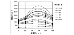
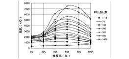
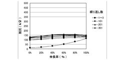
- the lowermost line in each figure represents the change in electrical resistance when extending to 100% in the first axial direction (during the forward pass), and the expansion rate is 100
- the other line (upper line) extending from the point representing the electrical resistance value at% represents the change in electrical resistance when returning from the first elongation rate of 100% to the elongation rate of 0% (on the return path).
- the number of repetitions is one for the forward and return routes.
- two lines whose resistance value at the time of 100% elongation extends from the second point from the bottom represents the change in the electric resistance of the second repetition number, and among these, the lower line is the outward path of the second repetition number.
- the upper line represents the change in electrical resistance during the second return.
- changes in electrical resistance after the third repetition are shown in FIGS.
- the single-walled carbon nanotubes with small fiber diameters are superior to the multi-walled carbon nanotubes with large fiber diameters.
- the ratio of carbon nanotubes was found to be better. Furthermore, it was found that the sensor sheet of Example 3 that does not contain a rubber component in the electrode layer has a particularly small change in electrical resistance even when the elongation exceeds 100 times, and is particularly excellent in durability.
- the electrical resistance increases only in the first measurement of 100% elongation, and thereafter the electrical resistance is stabilized.
- a deformation history can be added in advance after the electrode layer is applied.
- the detection method as the sensor of the present invention is a change in capacitance, the electrode layer has sufficient conductivity even in a deformed state, and the electric resistance value of the electrode layer does not affect the measured value. Therefore, according to the capacitive sensor sheet of the present invention, it is possible to provide a sensor that is excellent in repeated durability without having a step of adding a change history in advance.
- Example 2 and Example 4 containing an electrode layer elastomer the substantially same result as FIG.8 and FIG.9 was obtained, respectively.
- the sensor sheet of Comparative Example 1 was measurable up to an elongation rate of 50%, but became unmeasurable at 100% elongation.
- the sensor sheet of the example had less variation in the measured capacitance value after repeated deformation and was superior in repeatability compared to the comparative example.
- the sensor sheet of Example 1 and Example 3 in which the rubber component is not contained in the electrode layer is superior to the sensor sheet of Example 2 and Example 4 in which the rubber component is contained in the electrode layer, respectively, in terms of repeatability. I found out.
- the sensor sheet of Example 3 using carbon nanotubes with a high aspect ratio for the electrode layer was particularly excellent in repeatability. This is because by using long carbon nanotubes with a high aspect ratio, the carbon nanotubes can stretch and follow like a spring, and even if the sensor sheet is deformed, the conductive path is difficult to cut. It is inferred that the effect was remarkably expressed.
- the capacitance type sensor sheet used for measuring the amount of stretch deformation strain and / or distribution of stretch deformation strain of the present invention can follow the deformation and operation of a flexible measurement object having a large elongation, In addition, it is excellent in durability against stretching deformation and repeated deformation.
Landscapes
- Engineering & Computer Science (AREA)
- General Engineering & Computer Science (AREA)
- Theoretical Computer Science (AREA)
- Physics & Mathematics (AREA)
- General Physics & Mathematics (AREA)
- Human Computer Interaction (AREA)
- Power Engineering (AREA)
- Measurement Of Length, Angles, Or The Like Using Electric Or Magnetic Means (AREA)
- Force Measurement Appropriate To Specific Purposes (AREA)
Description
C=ε0εrS/d・・・(1)
ここで、Cはキャパシタンス、ε0は自由空間の誘電率、εrは誘電層の比誘電率、Sは電極層面積、dは電極間距離である。
エラストマー製の誘電層と、
上記誘電層の表面に積層される表側電極層と、
上記誘電層の裏面に積層される裏側電極層と
を備え、
上記表側電極層及び裏側電極層がカーボンナノチューブを含み、
上記表側電極層及び裏側電極層の平均厚みがそれぞれ0.1μm以上10μm以下であり、伸縮変形歪み量及び伸縮変形歪み分布を計測するために用いられる静電容量型センサシートである。
エラストマー材料により誘電層を形成する工程、及び
カーボンナノチューブを含む塗布液の塗布により、上記誘電層の
表面及び裏面に平均厚みがそれぞれ0.1μm以上10μm以下の電極層を積層する工程
を有する。
当該静電容量型センサシートと、
上記静電容量型センサシートの表側電極層及び裏側電極層に接続される検出回路と
を備える。
<静電容量型センサシート1>
図1の静電容量型センサシート1は、シート状の誘電層2と、上記誘電層2の表面に積層される帯状体の表側電極層01A~16Aと、上記誘電層2の裏面に積層される帯状体の裏側電極層01B~16Bと、表側配線01a~16aと、裏側配線01b~16bとを備える。上記表側電極層と裏側電極層とが表裏(上下)方向に交差する部分が検出部(以下、「画素」ともいう)C0101~C1616となる。なお、検出部(画素)の符号「C○○△△」中、上2桁の「○○」は、表側電極層01A~16Aに対応している。下2桁の「△△」は、裏側電極層01B~16Bに対応する。
誘電層2は、弾性変形可能な層である。誘電層2は、シート状を呈しており、X方向及びY方向を各辺とする平面視長方形状を有する。この誘電層2は主としてエラストマーから構成され、例えば天然ゴム、イソプレンゴム、ニトリルゴム(NBR)、エチレンプロピレンゴム(EPDM)、スチレン・ブタジエンゴム(SBR)、ブタジエンゴム(BR)、クロロプレンゴム(CR)、シリコーンゴム、フッ素ゴム、アクリルゴム、水素添加ニトリルゴム、ウレタンゴム等から構成することが可能である。誘電層2を構成するエラストマーとしては、高い伸び性を有し、繰り返し変形での耐性に優れ、永久歪み性が小さいシリコーンゴム、ウレタンゴムが好ましいが、測定対象物や計測目的に応じて材料を選択することができ、配合の改良を施すことが可能である。
表側電極層01A~16Aは、それぞれ帯状を呈しており、誘電層2の表面に合計16本積層されている。表側電極層01A~16Aは、それぞれX方向(左右方向)に延在している。表側電極層01A~16Aは、それぞれY方向(前後方向)に所定間隔ごとに離間して、互いに略平行となるようにそれぞれ配置されている。表側電極層01A~16Aの左端には、それぞれ表側接続部01A1~16A1が配置されている。
裏側電極層01B~16Bは、それぞれ帯状を呈しており、誘電層2の裏面に合計16本積層されている。裏側電極層01B~16Bは、それぞれ表側電極層01A~16Aと表裏方向から見て略直角で交差するように配置されている。すなわち、裏側電極層01B~16Bは、それぞれY方向に延在している。また、裏側電極層01B~16Bは、X方向に所定間隔ごとに離間して、互いに略平行となるようにそれぞれ配置されている。裏側電極層01B~16Bの前端には、それぞれ裏側接続部01B1~16B1が配置されている。
表側配線01a~16aは、線状を呈しており、それぞれ上記表側接続部01A1~16A1と検出回路とを接続する。表側配線01a~16aを構成する材料としては、特に限定されず、従来公知の材料を用いることができるが、上述した表側電極層01A~16Aと同様の構成のものとすることで表側配線01a~16aも伸縮変形でき、測定対象物によるセンサシートの変形を阻害しないため好ましい。即ち、導電性材料であるカーボンナノチューブ以外の含有割合を少なくすることが好ましく、エラストマー材料を含まない構成とすることがより好ましい。
裏側配線01b~16bは、線状を呈しており、それぞれ上記裏側接続部01B1~16B1と検出回路とを接続する。表側配線01a~16aを構成する材料については、上記表側配線01a~16aと略同様であるのでここでは説明を省略する。
検出部(画素)C0101~C1616は、図1にハッチングで示すように、表側電極層01A~16Aと、裏側電極層01B~16Bとが上下方向に交差する部分(重複する部分)に配置されている。検出部(画素)C0101~C1616は、合計256個(=16個×16個)配置されており、256画素となる。各画素から一対の電極層を取り出す場合、256×2極で512本の配線が必要となるが、本実施形態のように帯状電極を交差させることで、必要な配線数を16本+16本の32本とすることができる。これは、各16本の配線を外部の切替回路で切り替えることで、256画素を1画素ずつ切り替えながら静電容量を測定することによって可能となる。その結果、各画素の歪み量及びセンサシートの歪みの位置情報を検知することができる。検出部C0101~C1616は、静電容量型センサシート1の略全面に亘って、略等間隔に配置されている。検出部C0101~C1616は、それぞれ表側電極層01A~16Aの一部と、裏側電極層01B~16Bの一部と、誘電層2の一部とを備えている。
本発明の静電容量型センサシート1は、測定対象物載置前の静電容量Cと測定対象物載置後の静電容量Cから静電容量の変化量ΔCを検出し、伸縮変形歪み分布を求めることができる。本発明の静電容量型センサシート1は伸長度が大きく、1軸方向に100%まで繰り返し伸長させることが可能であり、また、300%まで伸長させてもシートが破壊されない。加えて、柔軟な測定対象物の変形や動作に追従することが可能で、かつ伸縮変形や繰り返し変形に対する耐久性に優れ、例えば測定対象物の形をトレースしたり、測定対象物の動きを直接的に検知すること等ができる。
次に、静電容量型センサシート1の製造方法について説明する。静電容量型センサシート1の製造方法は、
エラストマー材料により誘電層を形成する工程(以下、「誘電層形成工程」ともいう)、及び
カーボンナノチューブを含む塗布液の塗布により、上記誘電層の
表面及び裏面に平均厚みがそれぞれ0.1μm以上10μm以下の電極層を積層する工程(以下、「電極層積層工程」ともいう)
を有する。
本工程では、エラストマー材料により誘電層2を形成する。まず、エラストマーに必要に応じて、誘電フィラー、架橋剤、加硫促進剤、老化防止剤等を添加したエラストマー材料を調製する。エラストマー材料及び誘電層の形成方法は特に限定されず、従来公知の材料及び方法を用いることができるが、誘電層2を構成するエラストマーとして例えばウレタンゴムを用いる場合の誘電層2の製造工程の例を以下に述べる。ひまし油変性ポリオール(商品名「2T-5008S OHv=13.6」、豊国製油社製)、トリス(2-エチルヘキシル)トリメリット酸エステル可塑剤(商品名「TOTM」、大八化学社製)、酸化防止剤(商品名「Irganox 1010」、チバスペシャリティケミカルズ社製を計量し、80℃の減圧下において、95rpmで60分間撹拌混合する。次に、混合液を計量し、100℃に調整後、触媒(商品名「Ucat 2030」、サンアプロ社製)を添加し、アジターで1分間撹拌する。その後、所定量のイソシアネート(商品名「ミリオネートMT」、日本ポリウレタン工業社製)を添加し、アジターで90秒間撹拌後、即座に混合液を図12に示す成形装置に注入し、保護フィルムでサンドイッチ状にして搬送しつつ架橋硬化させ、保護フィルム付きの所定厚みのロール巻シートを得る。さらに、100℃に調節した炉で10~60分間架橋反応させることで、誘電層2を製造することができる。誘電層2は、通常10μm以上1000μm以下、好ましくは50μm以上500μm以下の平均厚みで形成される。
本工程では、カーボンナノチューブを含む塗布液の塗布により、上記誘電層2の表面及び裏面に平均厚みがそれぞれ0.1μm以上10μm以下の電極層を積層する。
本発明の静電容量型センサシートの製造方法によれば、上記表側電極層及び裏側電極層と誘電層との密着性をより向上することができ、センサシートが大きな伸縮変形や繰り返し変形を受けても、一対の電極層と誘電層との層間剥離をより抑制することができる。
本発明の伸縮変形歪み量及び/又は伸縮変形歪み分布を計測するために用いられるセンサは、
当該静電容量型センサシートと、
上記静電容量型センサシートの表側電極層及び裏側電極層に接続される検出回路と
を備える。
なお、本発明は上記実施態様の他、種々の変更、改良を施した形態で実施することができる。
EPDM(エスプレン600F、住友化学製)100質量部に、パーオキサイド架橋剤としてのパークミルD(日本油脂製)を1.1質量部添加し、ロール混練した生ゴムを得た。この生ゴムを160℃で20分間プレス成型して架橋させ、膜厚100μmの誘電層を作製した。
[調製例1]
カーボンナノチューブとしてVGCF-X(長さ3μm、アスペクト比約200、登録商標、昭和電工製)30質量部をメチルイソブチルケトン(MIBK)56,070質量部に添加し、ジェットミル分散処理を施して塗布液(A-1)を得た。
上記得られた塗布液(A-1)に、ゴム材料としてのフッ素ゴム(ダイエルTMG-912、ダイキン工業製)を2,113質量部さらに添加し、塗布液(A-2)を得た。
調製例1において、カーボンナノチューブとして、上記VGCF-Xの代わりにスーパーグロースCNT(以下、「SGCNT」とも表記する)(繊維径の中央値が約3nm、成長長さ500μm~700μm、アスペクト比約100,000、炭素純度99.9%、産業技術総合研究所提供)を用いた以外は調製例1と同様に操作して、塗布液(A-3)を得た。
カーボンナノチューブとして上記SGCNT30質量部をメチルイソブチルケトン(MIBK)56,070質量部に添加し、ジェットミル分散処理を施した塗布液に、ゴム材料としてのフッ素ゴム(ダイエルTMG-912、ダイキン工業製)を2,113質量部さらに添加し、塗布液(A-4)を得た。
EPDM(エスプレン600F、住友化学製)429質量部に対して、カーボンナノチューブとして上記VGCF-Xを30質量部、可塑剤として絶縁油(トランスフォーマーオイルG、出光興産製)607質量部、並びに硫黄架橋剤としての亜鉛華(ハクスイテック製)10.7質量部、ステアリン酸(花王ケミカル製)2.1質量部、セイミOT(日本乾溜工業製)3.6質量部、促進EM-2(三新化学工業製)6.0質量部及び促進MSA(大内新興化学工業製)2.6質量部を添加してロール混練し分散させ、プレス成型架橋して膜厚40μmの電極シート(a-1)を作製した。
[実施例1~4]
上記作製した誘電層の表面に、上記得られた各塗布液(A-1)~(A-4)をエアブラシで帯状に塗布して乾燥させた。帯状電極は平均厚みが約1μm、幅が10mm、長さが100mmのものを、5mm間隔で5本形成した。続いて、上記誘電層の裏面に、上記各塗布液を表面の帯状電極と直交するように塗布し同じ要領で形成させた。この帯状電極の両端を0.1mm厚の銅箔で補強し、外部配線のリード線をネジ止めして接続した。
また、上記電極シート(a-1)を帯状に裁断し、これを上記作製した誘電層の表面及び裏面に、表面の帯状電極と裏面の帯状電極が直交するように貼り合わせ、比較例1の静電容量型センサシートを作製した。各帯状電極層はそれぞれ平均厚みが40μm、幅が10mm、長さが100mmとなるように形成した。
上記作製した各静電容量型センサシートを用い、以下の評価を実施した。
1軸方向に100%まで伸長させる伸長変形を繰り返し行い、帯状電極の両端の電気抵抗を測定した。帯状電極は20mm幅で長さ50mmとした。まず、伸長を1軸方向に100%まで1回行い、変形履歴を加えた後、これを繰り返し行い、上記電気抵抗の変化を測定した。実施例1~4の結果をそれぞれ図3~図6に、比較例1の結果を図7に示す。電気抵抗の増加が小さいほど、導電性が低下せず繰り返し変形に対する耐久性が良好であると評価できる。ここで、図3~図7中、各図の一番下の線が、1回目の1軸方向に100%まで伸長する際(往路の際)の電気抵抗の変化を表し、その伸長率100%時の電気抵抗値を表す点から伸びる他方の線(より上方の線)が、1回目の伸長率100%から伸長率0%に戻る際(復路の際)の電気抵抗の変化を表す。この往路と復路を合わせて繰り返し数1回とした。同様にして、100%伸長時の抵抗値が下から2番目の点から伸びる二つの線が繰り返し数2回目の電気抵抗の変化を表し、これらのうち、下方の線が繰り返し数2回目の往路の際の、上方の線が繰り返し数2回目の復路の際の電気抵抗の変化を表す。同様にして、繰り返し数3回目以降の電気抵抗の変化を図3~図7に示す。
センサシートの変形に対する静電容量の変化を評価するために、実施例1~実施例4のセンサシートを図2のように2辺を樹脂フレームで拘束し、フレーム間を1軸方向に100%まで伸長させ静電容量の変化を測定した。静電容量の測定には、LCRメータ(日置電機製 LCRハイテスタ 3522-50)を用いた。25カ所の検出部の平均の静電容量を、1軸伸長の伸長率に対してプロットした。実施例1のセンサシートについては図8に、実施例3のセンサシートについては、図9に測定結果を示す。電極層エラストマーを含む実施例2及び実施例4については、それぞれ図8及び図9と略同じ結果が得られた。なお、比較例1のセンサシートについては、伸長率50%までは測定可能であったが、100%伸長では測定不能となった。
実施例1~実施例4のセンサシートについて、上述した1軸伸長を繰り返した時の静電容量の変化を測定し、繰り返し精度として評価した。この結果、実施例3>実施例4>実施例1>実施例2の順に繰り返し精度が優れることが分かった。実施例1のセンサシートについては図10に、実施例3のセンサシートについては図11に結果を示す。なお、比較例1のセンサシートは、1回の100%伸張履歴により導電性が失われたため、繰り返し精度を測定することができなかった。
2 誘電層
3 検出回路
01A1~16A1 表側接続部
01A~16A 表側電極層
01a~16a 表側配線
01B1~16B1 裏側接続部
01B~16B 裏側電極層
01b~16b 裏側配線
C0101~C1616 検出部
21 静電容量型センサシート
22 誘電層
23 樹脂フレーム
01A’~05A’ 表側電極層
01A’1~05A’1 表側接続部
01B’~05B’ 裏側電極層
01B’1~05B’1 裏側接続部
C’0101~C’0505 検出部
31 誘電層
32、32’ 保護フィルム
33 ポリウレタン用混合液
34 架橋炉
35 巻取り機
Claims (10)
- エラストマー製の誘電層と、
上記誘電層の表面に積層される表側電極層と、
上記誘電層の裏面に積層される裏側電極層と
を備え、
上記表側電極層及び裏側電極層がカーボンナノチューブを含み、
上記表側電極層及び裏側電極層の平均厚みがそれぞれ0.1μm以上10μm以下であり、伸縮変形歪み量及び/又は伸縮変形歪み分布を計測するために用いられる静電容量型センサシート。 - 上記表側電極層及び裏側電極層が、カーボンナノチューブを含む塗布液の塗布により形成されている請求項1に記載の静電容量型センサシート。
- 上記カーボンナノチューブの平均長さが100μm以上である請求項1に記載の静電容量型センサシート。
- 上記表側電極層及び裏側電極層がそれぞれ複数の帯状体からなり、この表側電極層と裏側電極層とが表裏方向から見て略直角で交差するように配置されている請求項1に記載の静電容量型センサシート。
- 1軸方向の伸長率が30%以上である請求項1に記載の静電容量型センサシート。
- 上記表側電極層及び上記裏側電極層の全固形成分に対する上記カーボンナノチューブの含有量が50質量%以上である請求項1に記載の静電容量型センサシート。
- 上記表側電極層及び裏側電極層が、実質的にカーボンナノチューブのみからなる請求項1に記載の静電容量型センサシート。
- 上記カーボンナノチューブが単層カーボンナノチューブである請求項1に記載の静電容量型センサシート。
- エラストマー材料により誘電層を形成する工程、及び
カーボンナノチューブを含む塗布液の塗布により、上記誘電層の表面及び裏面に平均厚みがそれぞれ0.1μm以上10μm以下の電極層を積層する工程
を有する静電容量型センサシートの製造方法。 - 請求項1に記載の静電容量型センサシートと、
上記静電容量型センサシートの表側電極層及び裏側電極層に接続される検出回路と
を備える伸縮変形歪み量及び/又は伸縮変形歪み分布を計測するために用いられるセンサ。
Priority Applications (4)
| Application Number | Priority Date | Filing Date | Title |
|---|---|---|---|
| CN201380050906.8A CN104685316B (zh) | 2012-09-28 | 2013-07-02 | 电容量型传感器片、电容量型传感器片的制造方法及传感器 |
| EP13840686.3A EP2905574B1 (en) | 2012-09-28 | 2013-07-02 | Capacitance-type sensor sheet, method for manufacturing capacitance-type sensor sheet, and sensor |
| US14/431,282 US9658120B2 (en) | 2012-09-28 | 2013-07-02 | Capacitance-type sensor sheet, method for manufacturing capacitance-type sensor sheet, and sensor |
| KR1020157007584A KR102029094B1 (ko) | 2012-09-28 | 2013-07-02 | 정전 용량형 센서 시트, 정전 용량형 센서 시트의 제조 방법 및 센서 |
Applications Claiming Priority (4)
| Application Number | Priority Date | Filing Date | Title |
|---|---|---|---|
| JP2012218707 | 2012-09-28 | ||
| JP2012-218707 | 2012-09-28 | ||
| JP2013-076221 | 2013-04-01 | ||
| JP2013076221A JP5497222B2 (ja) | 2012-09-28 | 2013-04-01 | 静電容量型センサシート及び静電容量型センサシートの製造方法 |
Publications (1)
| Publication Number | Publication Date |
|---|---|
| WO2014050245A1 true WO2014050245A1 (ja) | 2014-04-03 |
Family
ID=50387662
Family Applications (1)
| Application Number | Title | Priority Date | Filing Date |
|---|---|---|---|
| PCT/JP2013/068143 Ceased WO2014050245A1 (ja) | 2012-09-28 | 2013-07-02 | 静電容量型センサシート、静電容量型センサシートの製造方法及びセンサ |
Country Status (7)
| Country | Link |
|---|---|
| US (1) | US9658120B2 (ja) |
| EP (1) | EP2905574B1 (ja) |
| JP (1) | JP5497222B2 (ja) |
| KR (1) | KR102029094B1 (ja) |
| CN (1) | CN104685316B (ja) |
| TW (1) | TWI491862B (ja) |
| WO (1) | WO2014050245A1 (ja) |
Cited By (7)
| Publication number | Priority date | Publication date | Assignee | Title |
|---|---|---|---|---|
| WO2015156174A1 (ja) * | 2014-04-09 | 2015-10-15 | バンドー化学株式会社 | センサ装置 |
| JP2015200592A (ja) * | 2014-04-09 | 2015-11-12 | バンドー化学株式会社 | 静電容量型センサシート及び静電容量型センサ |
| WO2016063783A1 (ja) * | 2014-10-22 | 2016-04-28 | バンドー化学株式会社 | 静電容量型センサ |
| CN108209900A (zh) * | 2017-12-29 | 2018-06-29 | 中国科学院电子学研究所 | 颅内压力传感器、检测设备及制备方法 |
| JP2020046387A (ja) * | 2018-09-21 | 2020-03-26 | Nissha株式会社 | 圧力センサーシート |
| EP3185757B1 (en) * | 2014-08-25 | 2023-06-07 | Bainisha CVBA | Elastic sensor |
| JP2023548702A (ja) * | 2020-11-03 | 2023-11-20 | 智能容電(北京)科技有限公司 | フレキシブル可変コンデンサ及びその製造方法 |
Families Citing this family (26)
| Publication number | Priority date | Publication date | Assignee | Title |
|---|---|---|---|---|
| US9816800B2 (en) * | 2013-10-10 | 2017-11-14 | Stretchsense Limited | Method of fabrication of laminates of elastic material suitable for dielectric elastomer sensing |
| EP3076402B1 (en) * | 2013-11-28 | 2022-06-08 | Bando Chemical Industries, Ltd. | Stretchable electrode, sensor sheet and capacitive sensor |
| JP6554657B2 (ja) * | 2014-11-07 | 2019-08-07 | バンドー化学株式会社 | 静電容量型センサ、及び、回転角度の測定方法 |
| JP2016153729A (ja) * | 2015-02-20 | 2016-08-25 | 住友理工株式会社 | 変形量測定構造体 |
| JP6325482B2 (ja) * | 2015-04-06 | 2018-05-16 | バンドー化学株式会社 | 静電容量型センサシート及びセンサ装置 |
| KR101742240B1 (ko) * | 2015-08-31 | 2017-06-01 | 숭실대학교산학협력단 | 커패시터형 촉각센서 및 그 제조방법 |
| US9733062B2 (en) * | 2015-11-20 | 2017-08-15 | General Electric Company | Systems and methods for monitoring component strain |
| CN105606265B (zh) * | 2016-01-15 | 2018-07-17 | 浙江大学 | 一种基于液压力传导的柔性触觉传感器 |
| FI127245B (en) * | 2016-07-11 | 2018-02-15 | Forciot Oy | Force and / or pressure sensor |
| TWI623732B (zh) * | 2016-12-29 | 2018-05-11 | 台灣艾華電子工業股份有限公司 | 分層異向位移型拉伸感測器 |
| CN108253998B (zh) * | 2016-12-29 | 2020-07-14 | 台湾艾华电子工业股份有限公司 | 拉伸传感器 |
| US11614378B2 (en) | 2017-01-06 | 2023-03-28 | Direct-C Limited | Polymeric nanocomposite based sensor and coating systems and their applications |
| JP6505164B2 (ja) * | 2017-07-10 | 2019-04-24 | バンドー化学株式会社 | 静電容量型センサシート及びセンサ装置 |
| KR101876438B1 (ko) * | 2017-08-10 | 2018-07-10 | 숭실대학교산학협력단 | 점유탄성 탄성중합체 기반 커패시터형 촉각센서 |
| US10746014B2 (en) | 2018-02-09 | 2020-08-18 | Schlumberger Technology Corporation | Method and system for monitoring a condition of an elastic element used in a downhole tool |
| WO2019166635A1 (en) * | 2018-03-01 | 2019-09-06 | Universität Basel Vizerektorat Forschung | Dielectric elastomer transducer and corresponding fabrication process |
| US20210239545A1 (en) * | 2018-04-20 | 2021-08-05 | Direct-C Limited | Wide area sensors |
| JP7009309B2 (ja) * | 2018-06-01 | 2022-01-25 | 住友理工株式会社 | 手術台用の体圧分布センサシート |
| CN112513559A (zh) * | 2018-07-20 | 2021-03-16 | 帝人株式会社 | 传感器装置 |
| WO2020194931A1 (ja) * | 2019-03-27 | 2020-10-01 | 住友理工株式会社 | 静電容量結合方式センサ |
| CN110095211B (zh) * | 2019-05-24 | 2023-12-19 | 清华大学深圳研究生院 | 一种可拉伸触觉传感器阵列及其制备方法 |
| CN112014003B (zh) * | 2019-05-28 | 2022-03-18 | 华中科技大学 | 一种用于人体肌肉变形测量的柔性传感器及其制备方法 |
| CN113795740A (zh) * | 2019-06-26 | 2021-12-14 | 百医医材科技股份有限公司 | 压力感应系统及压力感应设定方法 |
| KR102259977B1 (ko) * | 2019-10-11 | 2021-06-02 | 한국생산기술연구원 | 신축감지 정전용량센서 및 이를 포함하는 보행분석 센싱 구조체 및 신축감지 정전용량센서의 제조방법 |
| CN111184532B (zh) * | 2020-04-09 | 2020-07-31 | 上海尽星生物科技有限责任公司 | 一种接触式柔性适形超声探头的超声系统及方法 |
| KR20230104364A (ko) * | 2021-12-30 | 2023-07-10 | 삼성디스플레이 주식회사 | 전자 장치 |
Citations (5)
| Publication number | Priority date | Publication date | Assignee | Title |
|---|---|---|---|---|
| JP2009528254A (ja) * | 2006-03-03 | 2009-08-06 | ザ ボード オブ トラスティーズ オブ ザ ユニヴァーシティー オブ イリノイ | 空間的に配列したナノチューブ及びナノチューブアレイの作製方法 |
| JP2010043881A (ja) | 2008-08-08 | 2010-02-25 | Tokai Rubber Ind Ltd | 静電容量型面圧分布センサ |
| JP2010244772A (ja) * | 2009-04-03 | 2010-10-28 | Sony Corp | 静電容量式タッチ部材及びその製造方法、並びに静電容量式タッチ検出装置 |
| JP2011017626A (ja) * | 2009-07-09 | 2011-01-27 | Sony Corp | 力学量検知部材及び力学量検知装置 |
| JP2011075322A (ja) * | 2009-09-29 | 2011-04-14 | Tokai Rubber Ind Ltd | 静電容量型センサ |
Family Cites Families (27)
| Publication number | Priority date | Publication date | Assignee | Title |
|---|---|---|---|---|
| JPH0278925A (ja) * | 1988-09-16 | 1990-03-19 | Yokohama Syst Kenkyusho:Kk | 静電容量型圧力センサ |
| JP2003075277A (ja) * | 2001-09-05 | 2003-03-12 | Omron Corp | 面状圧力センサ |
| JP4963159B2 (ja) * | 2004-11-19 | 2012-06-27 | 日本碍子株式会社 | 圧電/電歪デバイス |
| JP4743520B2 (ja) * | 2006-03-02 | 2011-08-10 | 三洋電機株式会社 | カーボンナノチューブ電極及びその製造方法 |
| JP2008113544A (ja) * | 2006-10-04 | 2008-05-15 | Tokai Rubber Ind Ltd | アクチュエータ |
| CN100420626C (zh) * | 2006-11-27 | 2008-09-24 | 西南交通大学 | 纯碳纳米管薄膜的制备方法 |
| JP5530585B2 (ja) * | 2007-01-31 | 2014-06-25 | 東海ゴム工業株式会社 | 電歪型アクチュエータ用誘電体エラストマー膜の製造方法 |
| JP4911702B2 (ja) * | 2007-01-31 | 2012-04-04 | 日本リニアックス株式会社 | 圧力センサ |
| JP4771971B2 (ja) * | 2007-02-09 | 2011-09-14 | 東海ゴム工業株式会社 | 柔軟電極およびそれを用いた電子機器 |
| JP2008252958A (ja) * | 2007-03-29 | 2008-10-16 | Kuraray Co Ltd | アクチュエータ及びそれに使用する電極 |
| JP2009189747A (ja) * | 2008-02-18 | 2009-08-27 | Goto Ikueikai | 歪センサ |
| TW201008118A (en) * | 2008-04-10 | 2010-02-16 | Atmel Corp | Capacitive touch screen with noise suppression |
| JP5479325B2 (ja) | 2008-04-18 | 2014-04-23 | 日本碍子株式会社 | 圧電/電歪デバイスの検査方法及び検査装置、並びに圧電/電歪デバイスの調整方法 |
| WO2009145080A1 (ja) * | 2008-05-24 | 2009-12-03 | 株式会社クラレ | タッチパネル |
| US7958789B2 (en) * | 2008-08-08 | 2011-06-14 | Tokai Rubber Industries, Ltd. | Capacitive sensor |
| JP5474331B2 (ja) * | 2008-10-30 | 2014-04-16 | 東海ゴム工業株式会社 | 誘電膜、およびそれを用いたアクチュエータ、センサ、トランスデューサ |
| JP4383505B1 (ja) * | 2009-05-15 | 2009-12-16 | 株式会社Hyper Drive | 発電効率及び耐久性が改善された電場応答性高分子 |
| EP2284933A1 (de) * | 2009-07-22 | 2011-02-16 | Bayer MaterialScience AG | Verfahren zur Herstellung von dehnbaren Elektroden |
| WO2011013256A1 (ja) * | 2009-07-28 | 2011-02-03 | 東京エレクトロン株式会社 | アクチュエータ素子及びアクチュエータ素子の製造方法 |
| JP5477624B2 (ja) * | 2009-09-02 | 2014-04-23 | 学校法人 名城大学 | 二層カーボンナノチューブを主体とする炭素質材料の製造方法 |
| KR101115419B1 (ko) * | 2009-09-08 | 2012-02-15 | 한국표준과학연구원 | 열접착 테이프를 이용한 정전용량형 힘 센서 제작방법 |
| JP5432207B2 (ja) * | 2011-04-19 | 2014-03-05 | 東海ゴム工業株式会社 | 静電容量型センサ装置 |
| JP4837794B1 (ja) * | 2011-05-30 | 2011-12-14 | 美紀夫 和氣 | 駆動性能及び耐久性が改善されたトランスデューサー用電場応答性高分子 |
| JP5831926B2 (ja) * | 2011-07-06 | 2015-12-09 | アルプス電気株式会社 | 高分子アクチュエータ素子及びその製造方法 |
| JP5757521B2 (ja) * | 2011-07-06 | 2015-07-29 | 国立研究開発法人産業技術総合研究所 | 油脂或いは撥水剤を含むアクチュエータ素子 |
| US9411472B2 (en) * | 2011-12-08 | 2016-08-09 | Atmel Corporation | Touch sensor with adaptive touch detection thresholding |
| JP3182167U (ja) * | 2012-11-01 | 2013-03-14 | スペースリンク株式会社 | コイン型カーボンナノチューブフィルムキャパシタ |
-
2013
- 2013-04-01 JP JP2013076221A patent/JP5497222B2/ja active Active
- 2013-07-02 KR KR1020157007584A patent/KR102029094B1/ko not_active Expired - Fee Related
- 2013-07-02 US US14/431,282 patent/US9658120B2/en not_active Expired - Fee Related
- 2013-07-02 EP EP13840686.3A patent/EP2905574B1/en not_active Not-in-force
- 2013-07-02 WO PCT/JP2013/068143 patent/WO2014050245A1/ja not_active Ceased
- 2013-07-02 CN CN201380050906.8A patent/CN104685316B/zh active Active
- 2013-07-29 TW TW102127115A patent/TWI491862B/zh not_active IP Right Cessation
Patent Citations (5)
| Publication number | Priority date | Publication date | Assignee | Title |
|---|---|---|---|---|
| JP2009528254A (ja) * | 2006-03-03 | 2009-08-06 | ザ ボード オブ トラスティーズ オブ ザ ユニヴァーシティー オブ イリノイ | 空間的に配列したナノチューブ及びナノチューブアレイの作製方法 |
| JP2010043881A (ja) | 2008-08-08 | 2010-02-25 | Tokai Rubber Ind Ltd | 静電容量型面圧分布センサ |
| JP2010244772A (ja) * | 2009-04-03 | 2010-10-28 | Sony Corp | 静電容量式タッチ部材及びその製造方法、並びに静電容量式タッチ検出装置 |
| JP2011017626A (ja) * | 2009-07-09 | 2011-01-27 | Sony Corp | 力学量検知部材及び力学量検知装置 |
| JP2011075322A (ja) * | 2009-09-29 | 2011-04-14 | Tokai Rubber Ind Ltd | 静電容量型センサ |
Non-Patent Citations (1)
| Title |
|---|
| See also references of EP2905574A4 |
Cited By (16)
| Publication number | Priority date | Publication date | Assignee | Title |
|---|---|---|---|---|
| EP3868295A1 (en) * | 2014-04-09 | 2021-08-25 | Bando Chemical Industries, Ltd. | Method of tracing a deformation of a surface of a living body |
| TWI642408B (zh) * | 2014-04-09 | 2018-12-01 | 日商阪東化學股份有限公司 | Sensing device |
| WO2015156174A1 (ja) * | 2014-04-09 | 2015-10-15 | バンドー化学株式会社 | センサ装置 |
| JP6053988B2 (ja) * | 2014-04-09 | 2016-12-27 | バンドー化学株式会社 | センサ装置 |
| JP2017047273A (ja) * | 2014-04-09 | 2017-03-09 | バンドー化学株式会社 | センサ装置 |
| JP2015200592A (ja) * | 2014-04-09 | 2015-11-12 | バンドー化学株式会社 | 静電容量型センサシート及び静電容量型センサ |
| EP3185757B1 (en) * | 2014-08-25 | 2023-06-07 | Bainisha CVBA | Elastic sensor |
| JPWO2016063783A1 (ja) * | 2014-10-22 | 2017-08-03 | バンドー化学株式会社 | 静電容量型センサ |
| CN107110634A (zh) * | 2014-10-22 | 2017-08-29 | 阪东化学株式会社 | 静电电容型传感器 |
| EP3211364A4 (en) * | 2014-10-22 | 2018-05-16 | Bando Chemical Industries, Ltd. | Capacitance sensor |
| US10337849B2 (en) | 2014-10-22 | 2019-07-02 | Bando Chemical Industries, Ltd. | Capacitive sensor |
| WO2016063783A1 (ja) * | 2014-10-22 | 2016-04-28 | バンドー化学株式会社 | 静電容量型センサ |
| CN108209900A (zh) * | 2017-12-29 | 2018-06-29 | 中国科学院电子学研究所 | 颅内压力传感器、检测设备及制备方法 |
| JP2020046387A (ja) * | 2018-09-21 | 2020-03-26 | Nissha株式会社 | 圧力センサーシート |
| JP2023548702A (ja) * | 2020-11-03 | 2023-11-20 | 智能容電(北京)科技有限公司 | フレキシブル可変コンデンサ及びその製造方法 |
| US12542244B2 (en) | 2020-11-03 | 2026-02-03 | Zhi Neng Rong Dian (Beijing) Technology Co., Ltd | Flexible variable capacitor and method for preparation thereof |
Also Published As
| Publication number | Publication date |
|---|---|
| EP2905574A1 (en) | 2015-08-12 |
| KR20150058256A (ko) | 2015-05-28 |
| KR102029094B1 (ko) | 2019-10-07 |
| EP2905574A4 (en) | 2016-06-22 |
| US20150268106A1 (en) | 2015-09-24 |
| EP2905574B1 (en) | 2018-09-26 |
| JP2014081355A (ja) | 2014-05-08 |
| CN104685316B (zh) | 2017-11-03 |
| CN104685316A (zh) | 2015-06-03 |
| TW201418686A (zh) | 2014-05-16 |
| TWI491862B (zh) | 2015-07-11 |
| US9658120B2 (en) | 2017-05-23 |
| JP5497222B2 (ja) | 2014-05-21 |
Similar Documents
| Publication | Publication Date | Title |
|---|---|---|
| JP5497222B2 (ja) | 静電容量型センサシート及び静電容量型センサシートの製造方法 | |
| WO2015029955A1 (ja) | 静電容量型センサシート及び静電容量型センサ | |
| US10365171B2 (en) | Capacitive sensor sheet and capacitive sensor for measuring elastic deformation | |
| JP6726781B2 (ja) | 伸縮性電極、センサシート及び静電容量型センサ | |
| JP6168912B2 (ja) | 伸縮性電極及びセンサシート | |
| JP5448423B2 (ja) | 触覚センサおよびその製造方法 | |
| JP5448736B2 (ja) | 導電膜、およびそれを備えたトランスデューサ、フレキシブル配線板 | |
| US9504151B2 (en) | Conductive composition and conductive film | |
| JP2009020006A (ja) | 静電容量型センサ | |
| JP6313100B2 (ja) | 静電容量型センサシート及び静電容量型センサ | |
| KR20170074914A (ko) | 정전 용량형 센서 | |
| JP2015059845A (ja) | 静電容量型センサ、及び伸縮変形歪み量、伸縮変形歪み分布又は面圧分布の計測方法 | |
| JP2014219263A (ja) | 静電容量型センサシート及び静電容量型センサ | |
| JP2014219214A (ja) | 静電容量型センサシート及び静電容量型センサ | |
| JP2015197382A (ja) | 静電容量型センサ、及び歪み計測装置 | |
| JP6574831B2 (ja) | 静電容量型センサシート及び静電容量型センサ |
Legal Events
| Date | Code | Title | Description |
|---|---|---|---|
| 121 | Ep: the epo has been informed by wipo that ep was designated in this application |
Ref document number: 13840686 Country of ref document: EP Kind code of ref document: A1 |
|
| ENP | Entry into the national phase |
Ref document number: 20157007584 Country of ref document: KR Kind code of ref document: A |
|
| WWE | Wipo information: entry into national phase |
Ref document number: 14431282 Country of ref document: US |
|
| NENP | Non-entry into the national phase |
Ref country code: DE |
|
| WWE | Wipo information: entry into national phase |
Ref document number: 2013840686 Country of ref document: EP |