WO2014057807A1 - ケーブル、電子機器及び電子機器の制御方法 - Google Patents
ケーブル、電子機器及び電子機器の制御方法 Download PDFInfo
- Publication number
- WO2014057807A1 WO2014057807A1 PCT/JP2013/075911 JP2013075911W WO2014057807A1 WO 2014057807 A1 WO2014057807 A1 WO 2014057807A1 JP 2013075911 W JP2013075911 W JP 2013075911W WO 2014057807 A1 WO2014057807 A1 WO 2014057807A1
- Authority
- WO
- WIPO (PCT)
- Prior art keywords
- cable
- electronic device
- light
- receptacle
- electrical contact
- Prior art date
- Legal status (The legal status is an assumption and is not a legal conclusion. Google has not performed a legal analysis and makes no representation as to the accuracy of the status listed.)
- Ceased
Links
Images





Classifications
-
- H—ELECTRICITY
- H01—ELECTRIC ELEMENTS
- H01B—CABLES; CONDUCTORS; INSULATORS; SELECTION OF MATERIALS FOR THEIR CONDUCTIVE, INSULATING OR DIELECTRIC PROPERTIES
- H01B11/00—Communication cables or conductors
- H01B11/18—Coaxial cables; Analogous cables having more than one inner conductor within a common outer conductor
- H01B11/1891—Coaxial cables; Analogous cables having more than one inner conductor within a common outer conductor comprising auxiliary conductors
-
- G—PHYSICS
- G02—OPTICS
- G02B—OPTICAL ELEMENTS, SYSTEMS OR APPARATUS
- G02B6/00—Light guides; Structural details of arrangements comprising light guides and other optical elements, e.g. couplings
- G02B6/44—Mechanical structures for providing tensile strength and external protection for fibres, e.g. optical transmission cables
- G02B6/4401—Optical cables
- G02B6/4415—Cables for special applications
- G02B6/4416—Heterogeneous cables
-
- G—PHYSICS
- G02—OPTICS
- G02B—OPTICAL ELEMENTS, SYSTEMS OR APPARATUS
- G02B6/00—Light guides; Structural details of arrangements comprising light guides and other optical elements, e.g. couplings
- G02B6/24—Coupling light guides
- G02B6/36—Mechanical coupling means
- G02B6/38—Mechanical coupling means having fibre to fibre mating means
- G02B6/3807—Dismountable connectors, i.e. comprising plugs
- G02B6/381—Dismountable connectors, i.e. comprising plugs of the ferrule type, e.g. fibre ends embedded in ferrules, connecting a pair of fibres
- G02B6/3817—Dismountable connectors, i.e. comprising plugs of the ferrule type, e.g. fibre ends embedded in ferrules, connecting a pair of fibres containing optical and electrical conductors
-
- G—PHYSICS
- G02—OPTICS
- G02B—OPTICAL ELEMENTS, SYSTEMS OR APPARATUS
- G02B6/00—Light guides; Structural details of arrangements comprising light guides and other optical elements, e.g. couplings
- G02B6/24—Coupling light guides
- G02B6/36—Mechanical coupling means
- G02B6/38—Mechanical coupling means having fibre to fibre mating means
- G02B6/3807—Dismountable connectors, i.e. comprising plugs
- G02B6/3873—Connectors using guide surfaces for aligning ferrule ends, e.g. tubes, sleeves, V-grooves, rods, pins, balls
- G02B6/3885—Multicore or multichannel optical connectors, i.e. one single ferrule containing more than one fibre, e.g. ribbon type
-
- G—PHYSICS
- G02—OPTICS
- G02B—OPTICAL ELEMENTS, SYSTEMS OR APPARATUS
- G02B6/00—Light guides; Structural details of arrangements comprising light guides and other optical elements, e.g. couplings
- G02B6/24—Coupling light guides
- G02B6/42—Coupling light guides with opto-electronic elements
- G02B6/4292—Coupling light guides with opto-electronic elements the light guide being disconnectable from the opto-electronic element, e.g. mutually self aligning arrangements
- G02B6/4293—Coupling light guides with opto-electronic elements the light guide being disconnectable from the opto-electronic element, e.g. mutually self aligning arrangements hybrid electrical and optical connections for transmitting electrical and optical signals
-
- H—ELECTRICITY
- H01—ELECTRIC ELEMENTS
- H01R—ELECTRICALLY-CONDUCTIVE CONNECTIONS; STRUCTURAL ASSOCIATIONS OF A PLURALITY OF MUTUALLY-INSULATED ELECTRICAL CONNECTING ELEMENTS; COUPLING DEVICES; CURRENT COLLECTORS
- H01R13/00—Details of coupling devices of the kinds covered by groups H01R12/70 or H01R24/00 - H01R33/00
- H01R13/62—Means for facilitating engagement or disengagement of coupling parts or for holding them in engagement
- H01R13/629—Additional means for facilitating engagement or disengagement of coupling parts, e.g. aligning or guiding means, levers, gas pressure electrical locking indicators, manufacturing tolerances
- H01R13/631—Additional means for facilitating engagement or disengagement of coupling parts, e.g. aligning or guiding means, levers, gas pressure electrical locking indicators, manufacturing tolerances for engagement only
-
- H—ELECTRICITY
- H01—ELECTRIC ELEMENTS
- H01R—ELECTRICALLY-CONDUCTIVE CONNECTIONS; STRUCTURAL ASSOCIATIONS OF A PLURALITY OF MUTUALLY-INSULATED ELECTRICAL CONNECTING ELEMENTS; COUPLING DEVICES; CURRENT COLLECTORS
- H01R13/00—Details of coupling devices of the kinds covered by groups H01R12/70 or H01R24/00 - H01R33/00
- H01R13/66—Structural association with built-in electrical component
- H01R13/70—Structural association with built-in electrical component with built-in switch
- H01R13/703—Structural association with built-in electrical component with built-in switch operated by engagement or disengagement of coupling parts, e.g. dual-continuity coupling part
-
- H—ELECTRICITY
- H01—ELECTRIC ELEMENTS
- H01R—ELECTRICALLY-CONDUCTIVE CONNECTIONS; STRUCTURAL ASSOCIATIONS OF A PLURALITY OF MUTUALLY-INSULATED ELECTRICAL CONNECTING ELEMENTS; COUPLING DEVICES; CURRENT COLLECTORS
- H01R2103/00—Two poles
Definitions
- the present disclosure relates to a cable, an electronic device, and an electronic device control method.
- SD image quality standard image quality
- HD image quality high-definition image quality
- 4K2K high-definition image quality
- the present disclosure provides a new and improved photoelectric composite cable, electronic device, and electronic device control capable of realizing a safe, low-cost, compact, and high-speed optical interface. It is to provide a method.
- At least one optical fiber cable at least two electrical cables provided so as to sandwich the optical fiber cable, and electrical contact portions located at both ends and connected to each of the electrical cables And a plug having a cable.
- At least two electrical contacts and a receptacle having at least one light emitting unit that emits laser light for performing light communication with an electronic device on the other side, and emission of the laser light from the light emitting unit
- a light-emission control unit that controls the light-emission control unit, wherein the light-emission control unit has a cable connected to the receptacle, and a current flows from the counterpart electronic device to the electrical contact, so that the current causes the light-emission unit to An electronic device is provided which starts controlling the emission of laser light.
- the receptacle having at least one electrical contact and at least one light receiving unit for receiving laser light for performing communication using light emitted from the counterpart electronic device, and the counterpart electronic device And a supply control unit that controls supply of current through the electrical contact, and the supply control unit starts supplying current through the electrical contact when a cable is connected to the receptacle.
- a cable is connected to a receptacle having at least two electrical contacts and at least one light emitting unit that emits laser light for performing optical communication with a counterpart electronic device, and the electrical contacts are connected to the electrical contacts.
- a method of controlling an electronic device comprising a step of starting control of light emission of the laser light from the light emitting unit by the current flowing from the electronic device on the other side.
- a method for controlling an electronic device comprising the step of starting supply of current through the electrical contact to the electronic device on the other side.
- the present disclosure is a new and improved cable, electronic device capable of realizing a safe, low-cost, small-sized optical interface capable of high-speed transmission.
- a method for controlling a device and an electronic device can be provided.
- FIG. 3 is an explanatory diagram illustrating a functional configuration example of a source device 2 configuring a system according to an embodiment of the present disclosure.
- 3 is an explanatory diagram illustrating a functional configuration example of a sink device 4 configuring a system according to an embodiment of the present disclosure.
- FIG. 6 is an explanatory diagram showing power feeding from the sink device 4 to the source device 2 via the cable 1.
- 5 is a flowchart showing an operation example of a source device 2 and a sink device 4.
- FIG. 2 is an explanatory diagram conceptually showing the structure of a plug 12 of a cable 1.
- FIG. It is explanatory drawing which shows the top and front view of the structural example of the plug. It is explanatory drawing which shows a mode that a plug and a receptacle are joined. It is explanatory drawing which shows a mode that a plug and a receptacle are joined.
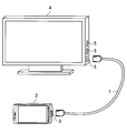
- FIG. 1 is an explanatory diagram illustrating an overall configuration example of a system including electronic devices connected by a cable according to an embodiment of the present disclosure.
- FIG. 1 is an explanatory diagram illustrating an overall configuration example of a system including electronic devices connected by a cable according to an embodiment of the present disclosure.
- FIG. 1 is an explanatory diagram illustrating an overall configuration example of a system including electronic devices connected by a cable according to an embodiment of the present disclosure.
- FIG. 1 is an explanatory diagram illustrating an overall configuration example of a system including electronic devices connected by a cable according to an embodiment of the present disclosure.
- the system includes a source device 2 and a sink device 4.
- the source device 2 and the sink device 4 are connected by a cable 1.
- the source device 2 is a small mobile device such as a smartphone or a digital camera shown in FIG.
- the sink device 4 is a television receiver in FIG.
- the source device 2 is provided with a source device-side receptacle 3 for connecting the cable 1
- the sink device 4 is provided with a sink device-side receptacle 5 for connecting the cable 1.
- the source device 2 and the sink device 4 shown in FIG. 1 are merely examples, and it goes without saying that the source device 2 and the sink device 4 are not limited to those shown in FIG.
- FIG. 1 shows a state in which a plurality of sink device side receptacles 5 (three in the figure) are provided in the sink device 4, but the present disclosure is not limited to such an example. Needless to say.
- source and sink are used in the same definition as “source” and “sink” in HDMI (High-Definition Multimedia Interface). That is, the source device 2 is a device that transmits data, and the sink device 4 is a device that receives data. The data stored in the source device 2 is transmitted to the sink device 4 through the cable 1 when the source device 2 and the sink device 4 are connected by the cable 1.
- the side that transmits data is defined as “source”
- the side that receives data is defined as “sink”.
- the cable 1 is a cable that connects the source device side receptacle 3 provided in the source device 2 that is an output source of video and audio and the sink device side receptacle 5 provided in the sink device 4.
- the cable 1 exchanges video data, audio data and other data, control signals, power, and the like between the source device 2 and the sink device 4.
- the cable 1 is provided with an optical fiber cable for high-speed data transmission between the source device 2 and the sink device 4.
- the cable 1 is also provided with an electric cable for transferring power between the source device 2 and the sink device 4.
- the width of the cable 1 and the size of the connector are desirably suppressed to a size that can be used for a small electronic device such as a digital camera or a smartphone.
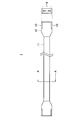
- FIG. 2 is an explanatory diagram illustrating a structure example of the cable 1 used in the system according to an embodiment of the present disclosure.
- a structural example of the cable 1 used in the system according to the embodiment of the present disclosure will be described with reference to FIG.
- the cable 1 includes two plugs 12 provided at both ends, two or more electrical contact portions 13 provided in each plug 12, and a plurality of optical contacts arranged in a row at approximately equal intervals. Part 14.
- the space between the two plugs 12 is constituted by a photoelectric composite cable wire 11 described later.
- the photoelectric composite cable wire 11 is composed of at least one, preferably a plurality of optical fiber cables, and two or more electric cables.
- the electrical cable is connected to the electrical contact portion 13.
- the plug 12 is a plug for connecting to the source device side receptacle 3 or the sink device side receptacle 5. Accordingly, the shape of the plug 12 is defined so as to match the shapes of the source device side receptacle 3 and the sink device side receptacle 5. Moreover, the electrical contact part 13 provided in the plug 12 is provided for transmission / reception of electric power between the source device 2 and the sink device 4 as described later. Needless to say, the shape of the plug 12 and the position of the electrical contact portion 13 provided on the plug 12 are not limited to those shown in FIG.
- FIG. 3 is an explanatory diagram illustrating a functional configuration example of the source device 2 configuring the system according to an embodiment of the present disclosure.
- a functional configuration example of the source device 2 will be described with reference to FIG.
- the source device 2 configuring the system according to an embodiment of the present disclosure includes an integrated chipset 22, a memory 23, a display unit 24, a signal conversion unit 27, and a laser drive circuit 35. And comprising.
- the source device side receptacle 3 provided in the source device 2 includes electrical contacts 31 and 32 and a plurality of light emitting units 34.
- the integrated chipset 22 controls the operation of the source device 2. There are various types of control of the operation of the source device 2 executed by the integrated chipset 22. For example, the integrated chipset 22 performs processing on content such as images and sounds provided from the source device 2 to the sink device 4. Various signal processing for providing to the sink device 4 is executed.
- the memory 23 stores various programs for controlling the operation of the source device 2, data used for operation control, and the like, and reads programs and data from the integrated chipset 22 as necessary.
- the display unit 24 displays images, characters, and other information, and includes, for example, a liquid crystal display or an organic EL display. The display unit 24 displays images, characters, and other information under the control of the integrated chipset 22.
- the signal converter 27 converts content data such as images and sounds into signals for driving the laser drive circuit 35.
- the signal generated by the signal converter 27 is supplied to the laser drive circuit 35.
- the laser drive circuit 35 causes the light emitting unit 34 of the source device side receptacle 3 to emit light based on the signal supplied from the signal converting unit 27.
- the light emitting unit 34 emits laser light by the laser drive circuit 35.
- the light emitting unit 34 is configured by, for example, an optical member such as a VCSEL (Vertical Cavity Surface Emitting LASER: vertical cavity surface emitting laser) element for transmitting a signal by light emission, a lens formed in combination with the VCSEL element, or the like. Is done.
- VCSEL Vertical Cavity Surface Emitting LASER: vertical cavity surface emitting laser
- the light emitting unit 34 is provided at a position corresponding to the optical contact of the plug of the cable 1. And the electrical contacts 31 and 32 are provided in the position which pinches
- the electrical contact 31 is an electrical contact that provides a predetermined potential, for example, a potential of +5 V
- the electrical contact 32 is an electrical contact having a GND potential.
- the electrical contact 31 for applying a potential of +5 V is connected to the positive power source 36 of the laser drive circuit 35.
- the GND electrical contact 32 is connected to the GND 37 of the laser drive circuit 35, and the laser drive circuit 35 is configured to be able to supply power.
- the function configuration example of the source device 2 has been described above with reference to FIG. Next, a functional configuration example of the sink device 4 configuring the system according to an embodiment of the present disclosure will be described.
- FIG. 4 is an explanatory diagram illustrating a functional configuration example of the sink device 4 configuring the system according to an embodiment of the present disclosure.
- a functional configuration example of the sink device 4 will be described with reference to FIG.
- the sink device 4 includes an integrated chip set 42, a drive circuit 43, a display unit 44, and a signal processing unit 53.
- the sink device-side receptacle 5 includes electrical contacts 51 and 52 and a plurality of light receiving portions 54.
- the integrated chip set 42 controls the operation of the sink device 4.
- the integrated chipset 42 performs signal processing for displaying content data such as images and sounds transmitted from the source device 2 via the cable 1 on the display unit 44, and provides the signal to the drive circuit 43.
- the drive circuit 43 acquires a signal from the integrated chipset 42 and generates a signal for driving the display unit 44.
- the display unit 44 is configured by, for example, a liquid crystal display or an organic EL display, and displays an image by being driven by the drive circuit 43.
- the sink device 4 includes one or more sink device-side receptacles 5, and each sink device-side receptacle 5 has a photodiode element and a photo diode for transmitting a signal by receiving light.
- a plurality of light receiving portions 54 made of an optical member such as a lens formed in combination with the diode element are provided so as to correspond to the optical contacts of the plug of the cable 1.
- Electrical contacts 51 and 52 are provided so as to sandwich the light receiving portion 54.
- the electrical contact 51 is an electrical contact that provides a potential of, for example, + 5V
- the electrical contact 52 is an electrical contact having a potential of GND.
- the plug 12 of the cable 1 When the plug 12 of the cable 1 is fitted into the sink device side receptacle 5, the electrical contacts 51 and 52 and the electrical contact portion 13 of the plug 12 come into contact with each other.
- the sink device 4 can supply power to the source device 2 through contact between the electrical contacts 51 and 52 and the electrical contact portion 13 of the plug 12.
- Content such as images and sounds provided by the source device 2 transmitted through the cable 1 is guided as an optical signal by an optical fiber core wire 17 of each channel of the cable 1 described later.
- the optical signal guided by the optical fiber core wire 17 is optically joined to the light receiving part 54 of each channel corresponding to the optical contact part 14 of each channel described later.
- the signal from the light receiving unit 54 is subjected to signal processing by the integrated chip set 42 after being subjected to processing such as amplification and parallelization by the signal processing unit 53, for example.
- the integrated chip set 42 supplies the signal after signal processing to the drive circuit 43, and the drive circuit 43 converts the signal into a signal suitable for driving the display unit 44. Then, the content of the image transmitted from the source device 2 is displayed on the display unit 44, and the sound transmitted from the source device 2 is emitted by a speaker (not shown).
- the function configuration example of the sink device 4 has been described above with reference to FIG. Next, light emission and power supply of the source device 2 by power supply via the cable 1 connecting the source device 2 and the sink device 4 will be described.
- FIG. 5 is an explanatory diagram showing power feeding from the sink device 4 to the source device 2 via the cable 1.
- the light emission and power supply of the source device 2 by power supply via the cable 1 will be described with reference to FIG.
- the cable 1 is provided with two plugs 12 at both ends, and each plug 12 is provided with two or more electrical contact portions 13.
- the cable 1 is provided with two or more electrical cables 15 that connect the electrical contact portions 13 provided on the plugs 12 at both ends.
- the sink device 4 includes the electrical contacts 51 and 52 on the sink device side receptacle 5 as described above.
- the electrical contact 51 is an electrical contact that provides a potential of, for example, + 5V
- the electrical contact 52 is an electrical contact having a potential of GND.
- the electrical contact portion 13 contacts the electrical contacts 31 and 32. With this contact, a potential of +5 V is applied to the laser drive circuit 35 on the source device side. Similarly, the GND side is also connected through the electric cable 15 of the cable 1. Therefore, the light emitting unit 34 of the source device 2 can be driven by the power supply from the sink device 4.
- the source device 2 and the sink device 4 are connected by the cable 1, when the power is supplied to the source device 2 using the electric cable 15 provided in the cable 1 or the source device 2 includes a battery, The battery can also be charged.
- the light emission and power feeding of the source device 2 by power feeding via the cable 1 have been described above with reference to FIG. Next, an operation example of the source device 2 and the sink device 4 when the source device 2 and the sink device 4 are connected by the cable 1 will be described.
- FIG. 6 is a flowchart illustrating an operation example of the source device 2 and the sink device 4 when the source device 2 and the sink device 4 are connected by the cable 1 in the system according to an embodiment of the present disclosure.
- an operation example of the source device 2 and the sink device 4 when the source device 2 and the sink device 4 are connected by the cable 1 will be described with reference to FIG.
- the sink device 4 When the cable 1 is not connected to the source device 2 and the sink device 4, the sink device 4 is in the standby mode (step S101). In the standby mode, the + 5V side electrical contact 51 of the sink device 4 is normally in the small current mode.
- the source device 2 and the sink device 4 stand by until the source device 2 and the sink device 4 are connected by the cable 1 (step S102).
- the sink device 4 detects that a current flows between the + 5V side electrical contact 51 and the GND side electrical contact 52.
- the connection with the source device 2 is detected via the cable 1 (step S103).
- the electrical contact 51 on the + 5V side on the sink device 4 side enters a mode in which a larger specified current value can be supplied than in the standby mode.
- the sink device 4 sends, to the source device 2, a pulse for notifying that the power supply is ready from the sink device 4 to the line to which +5 V is supplied from the sink device 4 in the electric cable 15 (Step S ⁇ b> 5. S104).
- the source device 2 that has received a pulse for notifying that the power supply is ready from the sink device 4 obtains a specified current value from the electrical contact 31 on the +5 V power source side and drives the laser drive circuit 35 ( Step S105).
- the source device 2 receives power from the sink device 4, the source device 2 enters a mode for receiving power from the sink device 4 (step S106).
- the sink device 4 that has detected the connection with the source device 2 via the cable 1 performs control from, for example, the integrated chipset 42 so as to activate the circuit of the light receiving unit 54 of the sink device side receptacle 5 (step S107). ).
- the source device 2 and the sink device 4 are driven in this way, when the cable 1 is disconnected, the connection by the electric cable 15 is opened, so that current is supplied from the sink device 4 to the source device 2. As a result, the oscillation of the laser beam from the light emitting section 34 of the source device side receptacle 3 stops.
- the sink device 4 that has detected the connection via the cable 1 activates the light receiving unit 54 of the sink device side receptacle 5, first, among the plurality of light receiving units 54 of the sink device 4, Only one predetermined priority channel may be activated.
- the signal from the light emitting unit 34 of the source device 2 corresponding to the priority channel in the light receiving unit 54 may include a designation signal that designates a channel that is actually scheduled to be used. .
- the source device 2 and the sink device 4 By operating the source device 2 and the sink device 4 in this way, only the light receiving unit necessary for data transmission between the source device 2 and the sink device 4 is energized, and the unnecessary light receiving unit is not energized. It becomes possible to suppress power consumption. In addition, by configuring the source device 2 and the sink device 4 in this way, it is possible to realize low power consumption during standby and low power consumption by partial driving of only a part of necessary channels. Become.
- a case where only some of the channels are partially driven for example, a case where the bit rate of a signal transmitted from the source device 2 to the sink device 4 is low can be considered.
- the bit rate of the signal transmitted from the source device 2 to the sink device 4 is low, it is not necessary to drive all the channels, and only the minimum channel corresponding to the bit rate of the signal is driven. To the sink device 4 can be transmitted.
- FIG. 7 is an explanatory view showing a shape example of a general optical ribbon
- FIG. 8 is an explanatory view showing a cross-sectional example of the cable 1.
- a general optical ribbon 19 In general, a plurality of optical fiber core wires 17 are arranged in a line, and in order to protect the optical fiber core wires 17 arranged in a line, an optical ribbon 19 is configured by covering a coating 18 made of resin around. Is done.
- the number of optical fiber core wires 17, for example, 2 cores, 4 cores, 8 cores, and 12 cores are generally considered, but the number of optical fiber core wires 17 is not limited to these.
- the photoelectric composite cable wire 11 that connects the two plugs 12 has an electric cable 15 in such a manner as to sandwich a plurality of optical fiber core wires 17. Further, when the cross section of the photoelectric composite cable wire 11 is viewed, as shown in FIG. 8, the covering portion 16 of the electric cable 15 sandwiching the optical fiber core wire 17 is determined from the thickness t of the covering 18 of the optical fiber core wire 17 portion. The diameter or thickness ⁇ D is thicker.
- the following effects are brought about by configuring the cable 1 in this way.
- the photoelectric composite cable wire 11 is always in contact with a flat surface such as a floor or a table
- the covering portion of the electric cable 15 comes into contact with the optical fiber core wire 17 and the optical fiber core wire covering 18.
- the effect of making it difficult to damage is brought about.
- the electrical cable 15 can be given a role as a dynamic holding member (tension member) when the photoelectric composite cable wire 11 is pulled.
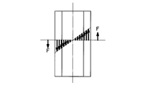
- FIG. 10, and FIG. 11 are explanatory views showing the case where the photoelectric composite cable wire 11 is twisted, bent horizontally, and bent vertically.
- the maximum is obtained in all cases where the photoelectric composite cable wire 11 is twisted or bent horizontally or vertically.
- the displacement and force F are proportional to the distance of the axis serving as the center of bending. Therefore, when the photoelectric composite cable wire 11 is twisted or bent horizontally or vertically, the maximum displacement and the force F are applied by the electric cable 15 and the covering portion 16 of the electric cable 15. 1 has the effect of preventing the generation of excessive stress on the optical fiber core wire 17 and its coating 18.
- FIG. 12 is an explanatory diagram showing a state in which the cable 1 is about to be cut by scissors.
- the cable 1 is cut by, for example, scissors, a cutter, or a sharp corner
- the peripheral electric cable 15 and the covering portion 16 of the electric cable 15 are first cut. Therefore, the optical fiber core wire 17 and the optical fiber core wire covering 18 are cut after the electric cable 15 and the covering portion 16 of the electric cable 15 are cut.
- the photoelectric composite cable wire 11 is cut in a state where the source device 2 and the sink device 4 are connected with the cable 1, the electric cable 15 is cut first, so that the sink device 4 Therefore, the power supply to the source device 2 is interrupted, and the oscillation (light emission) of the laser beam of the source device 2 is stopped. That is, in a state where the cable 1 is cut in whole or in part, infrared rays or visible light that may be harmful because of high energy density for the human eye will not come out of the cut surface of the cable 1. Disappear.
- the plug 12 is not pierced into the sink device-side receptacle 5, infrared light or visible light is not emitted from the end face of the plug 12 or the optical contact portion 14. Therefore, even if the photoelectric composite cable wire 11 is cut in a state where the source device 2 and the sink device 4 are connected by the cable 1, eye safety can be realized.
- FIG. 13 is an explanatory diagram conceptually showing an example of a structure with the plug 12 of the cable 1.
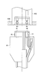
- FIG. 14 is an explanatory view showing a plan view and a front view of another structural example of the plug 12.
- the photoelectric composite cable wire 11 is provided with the electric cable 15 so as to sandwich the plurality of optical fiber core wires 17. Therefore, as the structure of the plug 12, for example, a form as shown in FIG.
- FIG. 13 shows the internal structure of the plug 12.
- a plurality of optical fiber core wires 17 are arranged in a line, and a member of the optical contact portion 14 is provided on the front surface of the optical fiber core wire 17.
- FIG. 14 shows another example of the structure of the plug 12.
- a plurality of optical fiber core wires 17 are arranged in a line, and on the front surface thereof, the members of the optical contact portion 14 are configured to have positioning holes 61 and 62 on both sides.
- FIG. 14 shows only the right half of the plug 12 so that the internal structure of the plug 12 can be seen.
- the electrical contact portion 13 having a spring element enters the positioning holes 61 and 62 from the opposite side surface where the optical fiber core wire 17 of the positioning holes 61 and 62 is located.
- the members of the optical contact portion 14 are formed of a plurality of channels integrally formed in a row, but the form of the optical contact portion in the cable of the present disclosure is as follows. It is not limited to such an example.
- FIG. 15A and FIG. 15B are explanatory views showing a state in which the plug 12 and the source device side receptacle 3 of the source device 2 or the sink device side receptacle 5 of the sink device 4 are joined in a plan view.
- 15A and 15B illustrate only the right half of the plug 12 so that the internal structure of the plug 12 can be seen.
- FIG. 15A shows a state before the plug 12 and the source device side receptacle 3 of the source device 2 or the sink device side receptacle 5 of the sink device 4 are joined.
- FIG. 15B shows a state after the plug 12 and the source device side receptacle 3 of the source device 2 or the sink device side receptacle 5 of the sink device 4 are joined.
- Positioning pins 63 and 64 are arranged on the source device side receptacle 3 or the sink device side receptacle 5.
- the positioning pins 63 and 64 serve as electrical contacts of the source device side receptacle 3 or the sink device side receptacle 5.
- the positioning pins 63 and 64 are inserted into the positioning holes 61 and 62 of the plug 12, and the electrical contact portion 13 having a spring element and By making contact, electrical conduction is performed and positioning is performed with respect to the insertion direction.
- optical contact portion 14 of the plug 12 is positioned with respect to the light emitting portion 34 of the source device 2 or the light receiving portion 54 of the sink device 4, so that light communication is performed between the source device 2 and the sink device 4. Is done.
- the photoelectric composite cable wire 11 has the two electric cables 15 (including the covering) and the optical ribbon 19 arranged outside at the base of the plug 12. Separate into three.
- the electrical cable 15 is electrically joined to the electrical contact portions 13 positioned outside the plurality of optical fiber core wires 17 by means of caulking or the like after the coating is peeled off.
- the plurality of optical fiber core wires 17 in the central portion become a plurality of optical contact portions 14 arranged at the same pitch as the pitch (core wire interval).
- the optical fiber core wire 17 has an optical contact portion formed integrally with a lens for condensing light of a plurality of channels arranged at the same pitch, and is spaced from each other by using a relative or an adhesive. It is also possible to adopt a configuration in which they are closely attached without being held.
- the size of the plug 12 of the cable 1 be relatively small, for example, equivalent to a micro USB (Universal Serial Bus) terminal. It is desirable to be formed in a size or smaller size.
- the shape of the plug 12 shown in FIG. 14 is an example, and the shape of the plug of the cable is not limited to this example in the present disclosure.
- the configuration in which two electrical contact portions 13 are provided in the plug 12 is shown, but the present disclosure is not limited to such an example.
- Three, four, or more electrical contact portions 13 may be present in the plug 12.
- a signal on the + 5V side is used as a minute differential signal
- a signal of an existing electrical interface such as a conventional MHL (Mobile High-definition Link) is used.
- the electric contact portion 13 may be allowed to flow.
- the electrical contact portion 13 may have a structure in which the entire positioning is performed using a polishing shaft. Moreover, you may provide the grinding
- the optical ribbon 19 does not necessarily have to be one line.
- 12 cores may be arranged in a line, or 4 cores may be arranged in 3 lines.
- the plurality of optical fiber core wires 17 can be configured to be opposed to the plurality of optical contact portions 14 arranged at the same pitch as the pitch (core wire interval).
- the photoelectric composite interface and the cable 1 used for the photoelectric composite interface can be configured. Then, by forming the source device side receptacle 3 of the cable 1 and the source device 2 and the sink device side receptacle 5 of the sink device 4 as described above, it is very realizable in the conventional interface between devices only with electricity. It is possible to realize an interface for a CE device that does not exist in the past and can perform ultra-high speed communication of several tens of Gbps to over 100 Gbps.
- the plug of the cable 1 can be reduced in size and thickness, the assembly cost can be reduced, and the manufacture at a low price can be realized.
- the cable 1, the source device 2, and the sink device 4 are safe and low-priced new devices that can cope with an increase in the transmission speed of uncompressed signals as the number of pixels in future displays increases.
- a photoelectric composite interface can be provided.
- this technique can also take the following structures.
- (3) The number of the optical fiber cables is two or more, and the cable according to (1) or (2), wherein a plurality of the optical fiber cables are provided in a line.
- a receptacle having at least one light emitting unit that emits laser light for performing optical communication with at least two electrical contacts and a partner electronic device;
- a light emission control unit for controlling light emission of the laser light from the light emitting unit; With The light emission control unit starts a control of light emission of the laser light from the light emitting unit by the current when a cable is connected to the receptacle and a current flows from the counterpart electronic device to the electrical contact.
- the light emission control unit emits light from only the minimum light emitting unit necessary for communication with the counterpart electronic device at the time of starting control of light emission of the laser light from the light emitting unit. ) Electronic device.
- a receptacle having at least one light receiving portion for receiving laser light for performing communication using light emitted from at least two electrical contacts and a counterpart electronic device;
- a supply control unit that controls supply of current through the electrical contacts to the electronic device on the other side;
- the said supply control part is an electronic device which starts supply of the electric current through the said electrical contact because a cable is connected to the said receptacle.
- a cable is connected to a receptacle having at least two electrical contacts and at least one light emitting unit that emits laser light for performing optical communication with the counterpart electronic device, and a current is supplied to the electrical contact from the counterpart electronic device.
- the control method of an electronic device is provided with the step which starts control of light emission of the laser beam from the said light emission part by this electric current by flowing.
- a cable is connected to a receptacle having at least two electrical contacts and at least one light receiving unit for receiving laser light for communication by light emitted from the other electronic device, the electronic device to the other electronic device
- a method for controlling an electronic device comprising a step of starting supply of current through the electrical contact.
- Cable 2 Source device 3: Source device side receptacle 4: Sink device 5: Sink device side receptacle 11: Photoelectric composite cable wire 12: Plug 13: Electric contact portion 14: Optical contact portion 15: Electric cable 16: Cover portion 17: Optical fiber core wire 18: Coating 19: Optical ribbon 22: Integrated chip set 23: Memory 24: Display unit 27: Signal conversion unit 31, 32: Electrical contact 34: Light emitting unit 35: Laser drive circuit 36: Positive power supply unit 42 : Integrated chip set 43: Drive circuit 44: Display units 51 and 52: Electrical contacts 53: Signal processing unit 54: Light receiving units 61 and 62: Positioning holes 63 and 64: Positioning pins
Landscapes
- Physics & Mathematics (AREA)
- General Physics & Mathematics (AREA)
- Optics & Photonics (AREA)
- Optical Couplings Of Light Guides (AREA)
- Connector Housings Or Holding Contact Members (AREA)
- Insulated Conductors (AREA)
- Semiconductor Lasers (AREA)
- Electromagnetism (AREA)
- Engineering & Computer Science (AREA)
- Computer Networks & Wireless Communication (AREA)
- Signal Processing (AREA)
- Communication Cables (AREA)
- Optical Communication System (AREA)
- Two-Way Televisions, Distribution Of Moving Picture Or The Like (AREA)
Abstract
Description
<1.本開示の一実施形態>
[システム構成例]
[ケーブルの構造例]
[ソース機器の機能構成例]
[シンク機器の機能構成例]
[ケーブルを介した給電]
[ソース機器及びシンク機器の動作例]
[ケーブルの形状例]
<2.まとめ>
[システム構成例]
まず、本開示の一実施形態に係るシステムの全体構成例について説明する。図1は、本開示の一実施形態に係るケーブルによって接続される電子機器で構成されるシステムの全体構成例を示す説明図である。以下、図1を参照して、本開示の一実施形態に係るシステムの全体構成例について説明する。
図2は、本開示の一実施形態に係るシステムで用いられるケーブル1の構造例を示す説明図である。以下、図2を用いて本開示の一実施形態に係るシステムで用いられるケーブル1の構造例について説明する。
図3は、本開示の一実施形態に係るシステムを構成するソース機器2の機能構成例を示す説明図である。以下、図3を用いてソース機器2の機能構成例について説明する。
図4は、本開示の一実施形態に係るシステムを構成するシンク機器4の機能構成例について示す説明図である。以下、図4を用いてシンク機器4の機能構成例について説明する。
図5は、ケーブル1を介したシンク機器4からソース機器2への給電について示す説明図である。以下、図5を用いて、ケーブル1を介した給電による、ソース機器2の発光及び給電について説明する。
図6は、本開示の一実施形態に係るシステムにおいて、ケーブル1によってソース機器2とシンク機器4とが接続された際の、ソース機器2及びシンク機器4の動作例を示す流れ図である。以下、図6を用いてケーブル1によってソース機器2とシンク機器4とが接続された際の、ソース機器2及びシンク機器4の動作例について説明する。
次に、本開示の一実施形態に係るシステムで用いられるケーブル1の形状例について説明する。図7は、一般的な光リボンの形状例を示す説明図であり、図8は、ケーブル1の断面例について示す説明図である。
以上説明したように本開示の一実施形態によれば、上述してきたように光電複合インターフェイスおよび、光電複合インターフェイスに使用するケーブル1を構成することができる。そして、ケーブル1及びソース機器2のソース機器側レセプタクル3並びにシンク機器4のシンク機器側レセプタクル5を、上述してきたような形状にすることにより、従来の電気のみの機器間インターフェイスにおいては実現が非常に困難であった数10Gbps~100Gbps超の超高速の通信が可能な、従来に存在しないCE機器向けのインターフェイスを実現することができる。
(1)
少なくとも1本の光ファイバケーブルと、
前記光ファイバケーブルを挟むように設けられる少なくとも2本の電気ケーブルと、
両端に位置し、前記電気ケーブルのそれぞれと接続される電気接点部を有するプラグと、
を備える、ケーブル。
(2)
前記電気ケーブルの被覆部の断面の径は、前記光ファイバケーブルの被覆部の厚さより長い、前記(1)に記載のケーブル。
(3)
前記光ファイバケーブルの本数は2本以上であり、複数本の前記光ファイバケーブルが一列に設けられる、前記(1)または(2)に記載のケーブル。
(4)
前記光ファイバケーブルの本数は2本以上であり、複数本の前記光ファイバケーブルが二列以上に設けられる、前記(1)~(3)のいずれかに記載のケーブル。
(5)
前記プラグは、レセプタクルに接合される際の位置決め部を備える、前記(1)~(4)のいずれかに記載のケーブル。
(6)
前記電気接点部は、前記プラグが前記レセプタクルに接合される際に前記位置決め部の内側に移動される、前記(5)に記載のケーブル。
(7)
前記電気接点部はバネ要素を持つ、前記(6)に記載のケーブル。
(8)
少なくとも2つの電気接点及び相手側の電子機器へ光による通信を行なうためのレーザー光を発光する少なくとも1つの発光部を有するレセプタクルと、
前記発光部からのレーザー光の発光を制御する発光制御部と、
を備え、
前記発光制御部は、前記レセプタクルにケーブルが接続され、前記電気接点に前記相手側の電子機器から電流が流れてくることで該電流により前記発光部からのレーザー光の発光の制御を開始する、電子機器。
(9)
前記発光制御部は、前記発光部からのレーザー光の発光の制御を開始した時点では前記相手側の電子機器との間の通信に必要な最低限の前記発光部のみから発光させる、前記(8)に記載の電子機器。
(10)
少なくとも2つの電気接点及び相手側の電子機器から発せられた光による通信を行なうためのレーザー光を受光する少なくとも1つの受光部を有するレセプタクルと、
前記相手側の電子機器へ前記電気接点を通じた電流の供給を制御する供給制御部と、
を備え、
前記供給制御部は、前記レセプタクルにケーブルが接続されることで前記電気接点を通じた電流の供給を開始する、電子機器。
(11)
少なくとも2つの電気接点及び相手側の電子機器へ光による通信を行なうためのレーザー光を発光する少なくとも1つの発光部を有するレセプタクルにケーブルが接続され、前記電気接点に前記相手側の電子機器から電流が流れてくることで該電流により前記発光部からのレーザー光の発光の制御を開始するステップを備える、電子機器の制御方法。
(12)
少なくとも2つの電気接点及び相手側の電子機器から発せられた光による通信を行なうためのレーザー光を受光する少なくとも1つの受光部を有するレセプタクルにケーブルが接続されると、前記相手側の電子機器へ前記電気接点を通じた電流の供給を開始するステップを備える、電子機器の制御方法。
2 :ソース機器
3 :ソース機器側レセプタクル
4 :シンク機器
5 :シンク機器側レセプタクル
11 :光電複合ケーブル線材
12 :プラグ
13 :電気接点部
14 :光接点部
15 :電気ケーブル
16 :被覆部
17 :光ファイバ芯線
18 :被覆
19 :光リボン
22 :統合チップセット
23 :メモリ
24 :表示部
27 :信号変換部
31、32:電気接点
34 :発光部
35 :レーザードライブ回路
36 :正極電源部
42 :統合チップセット
43 :駆動回路
44 :表示部
51、52:電気接点
53 :信号処理部
54 :受光部
61、62:位置決め穴部
63、64:位置決めピン
Claims (12)
- 少なくとも1本の光ファイバケーブルと、
前記光ファイバケーブルを挟むように設けられる少なくとも2本の電気ケーブルと、
両端に位置し、前記電気ケーブルのそれぞれと接続される電気接点部を有するプラグと、
を備える、ケーブル。 - 前記電気ケーブルの被覆部の断面の径は、前記光ファイバケーブルの被覆部の厚さより長い、請求項1に記載のケーブル。
- 前記光ファイバケーブルの本数は2本以上であり、複数本の前記光ファイバケーブルが一列に設けられる、請求項1に記載のケーブル。
- 前記光ファイバケーブルの本数は2本以上であり、複数本の前記光ファイバケーブルが二列以上に設けられる、請求項1に記載のケーブル。
- 前記プラグは、レセプタクルに接合される際の位置決め部を備える、請求項1に記載のケーブル。
- 前記電気接点部は、前記プラグが前記レセプタクルに接合される際に前記位置決め部の内側に移動される、請求項5に記載のケーブル。
- 前記電気接点部はバネ要素を持つ、請求項6に記載のケーブル。
- 少なくとも2つの電気接点及び相手側の電子機器へ光による通信を行なうためのレーザー光を発光する少なくとも1つの発光部を有するレセプタクルと、
前記発光部からのレーザー光の発光を制御する発光制御部と、
を備え、
前記発光制御部は、前記レセプタクルにケーブルが接続され、前記電気接点に前記相手側の電子機器から電流が流れてくることで該電流により前記発光部からのレーザー光の発光の制御を開始する、電子機器。 - 前記発光制御部は、前記発光部からのレーザー光の発光の制御を開始した時点では前記相手側の電子機器との間の通信に必要な最低限の前記発光部のみから発光させる、請求項8に記載の電子機器。
- 少なくとも2つの電気接点及び相手側の電子機器から発せられた光による通信を行なうためのレーザー光を受光する少なくとも1つの受光部を有するレセプタクルと、
前記相手側の電子機器へ前記電気接点を通じた電流の供給を制御する供給制御部と、
を備え、
前記供給制御部は、前記レセプタクルにケーブルが接続されることで前記電気接点を通じた電流の供給を開始する、電子機器。 - 少なくとも2つの電気接点及び相手側の電子機器へ光による通信を行なうためのレーザー光を発光する少なくとも1つの発光部を有するレセプタクルにケーブルが接続され、前記電気接点に前記相手側の電子機器から電流が流れてくることで該電流により前記発光部からのレーザー光の発光の制御を開始するステップを備える、電子機器の制御方法。
- 少なくとも2つの電気接点及び相手側の電子機器から発せられた光による通信を行なうためのレーザー光を受光する少なくとも1つの受光部を有するレセプタクルにケーブルが接続されると、前記相手側の電子機器へ前記電気接点を通じた電流の供給を開始するステップを備える、電子機器の制御方法。
Priority Applications (10)
| Application Number | Priority Date | Filing Date | Title |
|---|---|---|---|
| RU2015112230A RU2665703C2 (ru) | 2012-10-10 | 2013-09-25 | Кабель, электронное устройство и способ управления электронным устройством |
| KR1020157007409A KR20150070108A (ko) | 2012-10-10 | 2013-09-25 | 케이블, 전자 기기 및 전자 기기의 제어 방법 |
| CA2887200A CA2887200A1 (en) | 2012-10-10 | 2013-09-25 | Cable, electronic device, and method for controlling electronic device |
| BR112015007525A BR112015007525A2 (pt) | 2012-10-10 | 2013-09-25 | cabo, dispositivo eletrônico, e, método para controlar um dispositivo eletrônico |
| JP2014540797A JPWO2014057807A1 (ja) | 2012-10-10 | 2013-09-25 | ケーブル、電子機器及び電子機器の制御方法 |
| CN201380051984.XA CN104718583B (zh) | 2012-10-10 | 2013-09-25 | 线缆、电子装置以及用于控制电子装置的方法 |
| EP13844807.1A EP2897136B1 (en) | 2012-10-10 | 2013-09-25 | Photoelectric composite cable |
| US14/432,556 US9791650B2 (en) | 2012-10-10 | 2013-09-25 | Cable, electronic device, and method for controlling electronic device |
| US15/693,514 US10222567B2 (en) | 2012-10-10 | 2017-09-01 | Cable, electronic device, and method for controlling electronic device |
| US16/202,476 US10539755B2 (en) | 2012-10-10 | 2018-11-28 | Cable, electronic device, and method for controlling electronic device |
Applications Claiming Priority (2)
| Application Number | Priority Date | Filing Date | Title |
|---|---|---|---|
| JP2012224876 | 2012-10-10 | ||
| JP2012-224876 | 2012-10-10 |
Related Child Applications (2)
| Application Number | Title | Priority Date | Filing Date |
|---|---|---|---|
| US14/432,556 A-371-Of-International US9791650B2 (en) | 2012-10-10 | 2013-09-25 | Cable, electronic device, and method for controlling electronic device |
| US15/693,514 Division US10222567B2 (en) | 2012-10-10 | 2017-09-01 | Cable, electronic device, and method for controlling electronic device |
Publications (1)
| Publication Number | Publication Date |
|---|---|
| WO2014057807A1 true WO2014057807A1 (ja) | 2014-04-17 |
Family
ID=50477278
Family Applications (1)
| Application Number | Title | Priority Date | Filing Date |
|---|---|---|---|
| PCT/JP2013/075911 Ceased WO2014057807A1 (ja) | 2012-10-10 | 2013-09-25 | ケーブル、電子機器及び電子機器の制御方法 |
Country Status (9)
| Country | Link |
|---|---|
| US (3) | US9791650B2 (ja) |
| EP (1) | EP2897136B1 (ja) |
| JP (2) | JPWO2014057807A1 (ja) |
| KR (1) | KR20150070108A (ja) |
| CN (1) | CN104718583B (ja) |
| BR (1) | BR112015007525A2 (ja) |
| CA (1) | CA2887200A1 (ja) |
| RU (1) | RU2665703C2 (ja) |
| WO (1) | WO2014057807A1 (ja) |
Families Citing this family (14)
| Publication number | Priority date | Publication date | Assignee | Title |
|---|---|---|---|---|
| US12368615B2 (en) | 2013-09-19 | 2025-07-22 | Radius Universal Llc | Fiber optic communications and power network |
| US10139569B2 (en) * | 2016-04-05 | 2018-11-27 | Radius Universal, LLC | Connector assemblies for hybrid fiber/wire connections |
| US10277330B2 (en) | 2013-09-19 | 2019-04-30 | Radius Universal Llc | Fiber optic communications and power network |
| US10663672B2 (en) | 2016-04-05 | 2020-05-26 | Radius Universal Llc | Connector assemblies for hybrid fiber/wire connections |
| US10931915B2 (en) | 2016-06-01 | 2021-02-23 | Panasonic Intellectual Property Management Co., Ltd. | Transmission device, reception device, cable, transmission method, and reception method |
| CN106205853A (zh) * | 2016-08-30 | 2016-12-07 | 通鼎互联信息股份有限公司 | 一种usb3.1传输用光电复合缆 |
| CN107819636A (zh) * | 2016-09-13 | 2018-03-20 | 联想企业解决方案(新加坡)有限公司 | 用于定位数据电缆的装置和方法 |
| CN107104330A (zh) * | 2017-02-14 | 2017-08-29 | 珠海普生医疗科技有限公司 | 一种抗干扰的医用电缆 |
| CN109980708B (zh) * | 2017-12-28 | 2021-03-23 | 中国电信股份有限公司 | 供电装置、供电系统以及供电方法 |
| US10739541B2 (en) * | 2018-09-07 | 2020-08-11 | Corning Research & Development Corporation | Optical cable assemblies having variable output current limits |
| CN114664216B (zh) * | 2022-02-21 | 2022-10-18 | 北京富通亚讯网络信息技术有限公司 | 一种带mpo光纤功能的显示系统 |
| CN115185046A (zh) * | 2022-07-04 | 2022-10-14 | 京东科技信息技术有限公司 | 光源模块、初始化和控制方法以及装置 |
| CN115173167B (zh) * | 2022-07-15 | 2025-11-07 | Oppo广东移动通信有限公司 | 数据线及数据传输充电组件 |
| CN118570132A (zh) * | 2024-05-16 | 2024-08-30 | 南京莓跃霆网络科技有限公司 | 采用探入视觉检测的电力设备的电线管内部接头状态解析系统 |
Citations (12)
| Publication number | Priority date | Publication date | Assignee | Title |
|---|---|---|---|---|
| JPS6039514U (ja) * | 1983-08-26 | 1985-03-19 | トヨクニ電線株式会社 | 平型ケ−ブル |
| JPS6438910A (en) * | 1987-08-04 | 1989-02-09 | Mitsubishi Rayon Co | Flat type composite cable |
| JPH0737441A (ja) * | 1993-07-20 | 1995-02-07 | Fujikura Ltd | 複合プラグ付き電源・光複合コード |
| JP2000068938A (ja) * | 1998-06-10 | 2000-03-03 | Sony Corp | 光送受信装置 |
| JP2000214354A (ja) * | 1999-01-21 | 2000-08-04 | Toshiba Corp | 光ファイバコ―ドおよび光リンクシステム |
| JP2006157811A (ja) * | 2004-12-01 | 2006-06-15 | Fuji Xerox Co Ltd | 伝送エラーを減少させる光伝送方法及び光伝送装置 |
| JP2006310197A (ja) * | 2005-04-28 | 2006-11-09 | Sumitomo Electric Ind Ltd | 光dviケーブル及び光信号伝送装置 |
| JP2009048818A (ja) * | 2007-08-16 | 2009-03-05 | Hitachi Cable Ltd | 複合ケーブル |
| JP2009210906A (ja) * | 2008-03-05 | 2009-09-17 | Tomoegawa Paper Co Ltd | 光ファイバ集合体 |
| JP2010237640A (ja) | 2009-03-13 | 2010-10-21 | Fujikura Ltd | 光モジュールおよびモジュール付きケーブル |
| WO2011116167A1 (en) * | 2010-03-19 | 2011-09-22 | Corning Incorporated | Fiber optic interface device with translatable ferrule |
| JP2012054057A (ja) * | 2010-08-31 | 2012-03-15 | Japan Aviation Electronics Industry Ltd | 光電複合コネクタ及びそのレセプタクル |
Family Cites Families (19)
| Publication number | Priority date | Publication date | Assignee | Title |
|---|---|---|---|---|
| NL8403691A (nl) | 1984-12-05 | 1986-07-01 | Philips Nv | Optische verbindingsinrichting. |
| CN1007020B (zh) | 1985-07-15 | 1990-02-28 | Bicc公众有限公司 | 一种改进的光导纤维带结构 |
| JPS6344585U (ja) | 1986-09-10 | 1988-03-25 | ||
| JPH01148662U (ja) * | 1988-03-31 | 1989-10-16 | ||
| US4969924A (en) | 1989-05-18 | 1990-11-13 | General Motors Corporation | Electro-optical connector plug |
| US5109452A (en) * | 1990-07-16 | 1992-04-28 | Puritan-Bennett Corporation | Electrical-optical hybrid connector |
| ES2089319T3 (es) * | 1991-09-04 | 1996-10-01 | Furukawa Electric Co Ltd | Conector optico de nucleos multiples. |
| JPH0750638A (ja) | 1993-08-04 | 1995-02-21 | Hitachi Ltd | 光インタコネクト送信回路及び光インタコネクト送信装置 |
| US6618515B2 (en) * | 2000-06-21 | 2003-09-09 | Mitsubishi Cable Industries, Ltd. | Connector with a connection detection function, optical fiber cable with a connection detection function, and equipment control mechanism for an optical equipment |
| JP2007149499A (ja) | 2005-11-28 | 2007-06-14 | Teac Corp | コネクタ及びプラグ並びにジャック |
| US7272282B1 (en) * | 2006-07-31 | 2007-09-18 | Corning Cable Systems. Llc. | Fiber optic cables and assemblies suitable for distribution |
| US8380028B2 (en) * | 2009-05-18 | 2013-02-19 | Hitachi Cable, Ltd. | Composite cable |
| JP2010272417A (ja) | 2009-05-22 | 2010-12-02 | Hitachi Cable Ltd | 複合ケーブル |
| RU90058U1 (ru) * | 2009-10-14 | 2009-12-27 | Общество с ограниченной ответственностью "Научно-производственное предприятие "ЭГО" | Комбинированная линия связи между модулями системы безопасности грузоподъемного крана |
| CN102043204B (zh) | 2009-10-20 | 2012-12-19 | 富士康(昆山)电脑接插件有限公司 | 连接器 |
| CN102782545B (zh) | 2010-03-19 | 2015-07-08 | 康宁公司 | 用于电子装置的光纤接口装置 |
| US9046671B2 (en) | 2010-05-14 | 2015-06-02 | Sumitomo Electric Industries, Ltd. | Composite optical fiber cable and composite optical fiber cable assembly providing protection by flexure |
| US8774577B2 (en) * | 2010-12-07 | 2014-07-08 | Corning Cable Systems Llc | Optical couplings having coded magnetic arrays and devices incorporating the same |
| US8672559B2 (en) * | 2011-01-31 | 2014-03-18 | Avago Technologies General IP Singapore Pte. Ltd. | Thin connector assembly that has optical and electrical capabilities and that includes a plug having an optical surface that can be easily wiped clean |
-
2013
- 2013-09-25 CA CA2887200A patent/CA2887200A1/en not_active Abandoned
- 2013-09-25 WO PCT/JP2013/075911 patent/WO2014057807A1/ja not_active Ceased
- 2013-09-25 EP EP13844807.1A patent/EP2897136B1/en active Active
- 2013-09-25 JP JP2014540797A patent/JPWO2014057807A1/ja active Pending
- 2013-09-25 CN CN201380051984.XA patent/CN104718583B/zh active Active
- 2013-09-25 KR KR1020157007409A patent/KR20150070108A/ko not_active Ceased
- 2013-09-25 RU RU2015112230A patent/RU2665703C2/ru active
- 2013-09-25 US US14/432,556 patent/US9791650B2/en not_active Expired - Fee Related
- 2013-09-25 BR BR112015007525A patent/BR112015007525A2/pt not_active Application Discontinuation
-
2017
- 2017-09-01 US US15/693,514 patent/US10222567B2/en active Active
- 2017-10-30 JP JP2017209233A patent/JP2018074586A/ja active Pending
-
2018
- 2018-11-28 US US16/202,476 patent/US10539755B2/en active Active
Patent Citations (12)
| Publication number | Priority date | Publication date | Assignee | Title |
|---|---|---|---|---|
| JPS6039514U (ja) * | 1983-08-26 | 1985-03-19 | トヨクニ電線株式会社 | 平型ケ−ブル |
| JPS6438910A (en) * | 1987-08-04 | 1989-02-09 | Mitsubishi Rayon Co | Flat type composite cable |
| JPH0737441A (ja) * | 1993-07-20 | 1995-02-07 | Fujikura Ltd | 複合プラグ付き電源・光複合コード |
| JP2000068938A (ja) * | 1998-06-10 | 2000-03-03 | Sony Corp | 光送受信装置 |
| JP2000214354A (ja) * | 1999-01-21 | 2000-08-04 | Toshiba Corp | 光ファイバコ―ドおよび光リンクシステム |
| JP2006157811A (ja) * | 2004-12-01 | 2006-06-15 | Fuji Xerox Co Ltd | 伝送エラーを減少させる光伝送方法及び光伝送装置 |
| JP2006310197A (ja) * | 2005-04-28 | 2006-11-09 | Sumitomo Electric Ind Ltd | 光dviケーブル及び光信号伝送装置 |
| JP2009048818A (ja) * | 2007-08-16 | 2009-03-05 | Hitachi Cable Ltd | 複合ケーブル |
| JP2009210906A (ja) * | 2008-03-05 | 2009-09-17 | Tomoegawa Paper Co Ltd | 光ファイバ集合体 |
| JP2010237640A (ja) | 2009-03-13 | 2010-10-21 | Fujikura Ltd | 光モジュールおよびモジュール付きケーブル |
| WO2011116167A1 (en) * | 2010-03-19 | 2011-09-22 | Corning Incorporated | Fiber optic interface device with translatable ferrule |
| JP2012054057A (ja) * | 2010-08-31 | 2012-03-15 | Japan Aviation Electronics Industry Ltd | 光電複合コネクタ及びそのレセプタクル |
Non-Patent Citations (1)
| Title |
|---|
| See also references of EP2897136A4 |
Also Published As
| Publication number | Publication date |
|---|---|
| US9791650B2 (en) | 2017-10-17 |
| CN104718583A (zh) | 2015-06-17 |
| US20190094479A1 (en) | 2019-03-28 |
| CA2887200A1 (en) | 2014-04-17 |
| US10222567B2 (en) | 2019-03-05 |
| EP2897136A4 (en) | 2016-09-07 |
| JP2018074586A (ja) | 2018-05-10 |
| KR20150070108A (ko) | 2015-06-24 |
| EP2897136A1 (en) | 2015-07-22 |
| CN104718583B (zh) | 2018-01-26 |
| JPWO2014057807A1 (ja) | 2016-09-05 |
| RU2015112230A (ru) | 2016-10-20 |
| RU2665703C2 (ru) | 2018-09-04 |
| EP2897136B1 (en) | 2021-05-05 |
| US10539755B2 (en) | 2020-01-21 |
| US20180011272A1 (en) | 2018-01-11 |
| BR112015007525A2 (pt) | 2017-07-04 |
| US20150293322A1 (en) | 2015-10-15 |
Similar Documents
| Publication | Publication Date | Title |
|---|---|---|
| JP2018074586A (ja) | 電子機器及び電子機器の制御方法 | |
| JP7477524B2 (ja) | 光データ相互接続システムを起動する為の電池トリガ | |
| US11233569B2 (en) | Optical data interconnect system | |
| US11233570B2 (en) | Sink powered optical data interconnect system | |
| CN103630988B (zh) | 光电器件以及使用该光电器件的主动式光缆 | |
| CN201903673U (zh) | 光学模组、接口和光纤传输线 | |
| US11750294B2 (en) | Optical communication interface system | |
| US20060031611A1 (en) | Digital video signal interface module | |
| CN205139428U (zh) | 传输线结构 | |
| CN202854373U (zh) | 光电转换组件 | |
| JP2006189469A (ja) | 信号伝送用コネクタ及び光トランシーバ | |
| JP2013058335A (ja) | 光電気複合ケーブル | |
| JP2011138783A (ja) | ケーブル | |
| EP4125229A1 (en) | Optical communication interface system | |
| Liu et al. | Optical sub-assembly solution for single fiber optical HDMI connector | |
| TWI918983B (zh) | 光學通訊介面系統 | |
| CN115695739B (zh) | 光学通信介面系统 | |
| Schlepple et al. | Ultracompact 4× 3.4 Gbps optoelectronic package for an active optical HDMI cable | |
| JP2006109145A (ja) | 光伝送システム、装置接続方法、光ファイバーケーブル及び接続アダプター |
Legal Events
| Date | Code | Title | Description |
|---|---|---|---|
| 121 | Ep: the epo has been informed by wipo that ep was designated in this application |
Ref document number: 13844807 Country of ref document: EP Kind code of ref document: A1 |
|
| ENP | Entry into the national phase |
Ref document number: 20157007409 Country of ref document: KR Kind code of ref document: A |
|
| WWE | Wipo information: entry into national phase |
Ref document number: 14432556 Country of ref document: US |
|
| ENP | Entry into the national phase |
Ref document number: 2887200 Country of ref document: CA |
|
| ENP | Entry into the national phase |
Ref document number: 2014540797 Country of ref document: JP Kind code of ref document: A Ref document number: 2015112230 Country of ref document: RU Kind code of ref document: A |
|
| NENP | Non-entry into the national phase |
Ref country code: DE |
|
| REG | Reference to national code |
Ref country code: BR Ref legal event code: B01A Ref document number: 112015007525 Country of ref document: BR |
|
| ENP | Entry into the national phase |
Ref document number: 112015007525 Country of ref document: BR Kind code of ref document: A2 Effective date: 20150402 |