WO2014057893A1 - 検出方法、マイクロアレイの解析方法および蛍光読取装置 - Google Patents
検出方法、マイクロアレイの解析方法および蛍光読取装置 Download PDFInfo
- Publication number
- WO2014057893A1 WO2014057893A1 PCT/JP2013/077159 JP2013077159W WO2014057893A1 WO 2014057893 A1 WO2014057893 A1 WO 2014057893A1 JP 2013077159 W JP2013077159 W JP 2013077159W WO 2014057893 A1 WO2014057893 A1 WO 2014057893A1
- Authority
- WO
- WIPO (PCT)
- Prior art keywords
- light
- image data
- substrate
- fluorescence
- alignment
- Prior art date
- Legal status (The legal status is an assumption and is not a legal conclusion. Google has not performed a legal analysis and makes no representation as to the accuracy of the status listed.)
- Ceased
Links
Images











Classifications
-
- G—PHYSICS
- G01—MEASURING; TESTING
- G01N—INVESTIGATING OR ANALYSING MATERIALS BY DETERMINING THEIR CHEMICAL OR PHYSICAL PROPERTIES
- G01N21/00—Investigating or analysing materials by the use of optical means, i.e. using sub-millimetre waves, infrared, visible or ultraviolet light
- G01N21/62—Systems in which the material investigated is excited whereby it emits light or causes a change in wavelength of the incident light
- G01N21/63—Systems in which the material investigated is excited whereby it emits light or causes a change in wavelength of the incident light optically excited
- G01N21/64—Fluorescence; Phosphorescence
- G01N21/6486—Measuring fluorescence of biological material, e.g. DNA, RNA, cells
-
- G—PHYSICS
- G01—MEASURING; TESTING
- G01N—INVESTIGATING OR ANALYSING MATERIALS BY DETERMINING THEIR CHEMICAL OR PHYSICAL PROPERTIES
- G01N21/00—Investigating or analysing materials by the use of optical means, i.e. using sub-millimetre waves, infrared, visible or ultraviolet light
- G01N21/62—Systems in which the material investigated is excited whereby it emits light or causes a change in wavelength of the incident light
- G01N21/63—Systems in which the material investigated is excited whereby it emits light or causes a change in wavelength of the incident light optically excited
- G01N21/64—Fluorescence; Phosphorescence
- G01N21/645—Specially adapted constructive features of fluorimeters
- G01N21/6452—Individual samples arranged in a regular 2D-array, e.g. multiwell plates
-
- G—PHYSICS
- G01—MEASURING; TESTING
- G01N—INVESTIGATING OR ANALYSING MATERIALS BY DETERMINING THEIR CHEMICAL OR PHYSICAL PROPERTIES
- G01N21/00—Investigating or analysing materials by the use of optical means, i.e. using sub-millimetre waves, infrared, visible or ultraviolet light
- G01N21/62—Systems in which the material investigated is excited whereby it emits light or causes a change in wavelength of the incident light
- G01N21/63—Systems in which the material investigated is excited whereby it emits light or causes a change in wavelength of the incident light optically excited
- G01N21/64—Fluorescence; Phosphorescence
- G01N21/645—Specially adapted constructive features of fluorimeters
- G01N21/6456—Spatial resolved fluorescence measurements; Imaging
-
- G—PHYSICS
- G06—COMPUTING OR CALCULATING; COUNTING
- G06F—ELECTRIC DIGITAL DATA PROCESSING
- G06F17/00—Digital computing or data processing equipment or methods, specially adapted for specific functions
- G06F17/10—Complex mathematical operations
-
- G—PHYSICS
- G01—MEASURING; TESTING
- G01N—INVESTIGATING OR ANALYSING MATERIALS BY DETERMINING THEIR CHEMICAL OR PHYSICAL PROPERTIES
- G01N21/00—Investigating or analysing materials by the use of optical means, i.e. using sub-millimetre waves, infrared, visible or ultraviolet light
- G01N21/62—Systems in which the material investigated is excited whereby it emits light or causes a change in wavelength of the incident light
- G01N21/63—Systems in which the material investigated is excited whereby it emits light or causes a change in wavelength of the incident light optically excited
- G01N21/64—Fluorescence; Phosphorescence
- G01N21/6428—Measuring fluorescence of fluorescent products of reactions or of fluorochrome labelled reactive substances, e.g. measuring quenching effects, using measuring "optrodes"
- G01N2021/6439—Measuring fluorescence of fluorescent products of reactions or of fluorochrome labelled reactive substances, e.g. measuring quenching effects, using measuring "optrodes" with indicators, stains, dyes, tags, labels, marks
- G01N2021/6441—Measuring fluorescence of fluorescent products of reactions or of fluorochrome labelled reactive substances, e.g. measuring quenching effects, using measuring "optrodes" with indicators, stains, dyes, tags, labels, marks with two or more labels
-
- G—PHYSICS
- G01—MEASURING; TESTING
- G01N—INVESTIGATING OR ANALYSING MATERIALS BY DETERMINING THEIR CHEMICAL OR PHYSICAL PROPERTIES
- G01N2201/00—Features of devices classified in G01N21/00
- G01N2201/04—Batch operation; multisample devices
- G01N2201/0461—Simultaneous, e.g. video imaging
Definitions
- the present invention relates to a detection method for detecting a difference in height of uneven shapes on the surface of a microarray, a microarray analysis method, and a fluorescence reader.
- microarray is a substrate in which tens to tens of thousands of probes are fixed on a substrate such as glass or plastic.
- a sample (target) labeled with a fluorescent molecule is applied to the substrate, and the probe and This is for detecting the binding reaction by fluorescence or the like.
- Microarrays are capable of comprehensive measurements at once, and are expected to become essential for tailor-made medicine in the future.
- a DNA microarray (hereinafter referred to as a DNA chip) in which DNA is immobilized on a substrate as a probe, a protein microarray in which protein is immobilized on a substrate as a probe, a tissue microarray in which a large number of minute specimens are immobilized on a substrate as a probe, a large number of small molecules
- a DNA chip a DNA microarray in which DNA is immobilized on a substrate as a probe
- a protein microarray in which protein is immobilized on a substrate as a probe
- a tissue microarray in which a large number of minute specimens are immobilized on a substrate as a probe
- a large number of small molecules A compound microarray in which a compound is immobilized on a substrate as a probe is known.
- the DNA chip is most practically used, and research for searching for a gene related to a disease, and testing and diagnosis using the gene is actively conducted. Has been.
- a DNA chip is obtained by spotting (immobilizing) DNA in a grid shape on a substrate made of glass or resin.
- DNA probe single-stranded DNA
- a DNA probe having a known sequence is used.
- a DNA sample (single-stranded DNA) of an unknown sequence to be analyzed is attached with a luminescent or fluorescent mark that can be detected optically. In this way, when a DNA sample of an unknown sequence to be analyzed is poured onto a DNA chip, if the DNA sample sequence is complementary to the DNA probe sequence, the DNA probe and the DNA sample are linked together. It becomes strand DNA.
- FIG. 13 shows details of a series of processing steps of DNA chip analysis.
- a DNA sample provided with a fluorescent mark is dropped on the substrate of a DNA chip on which various types of DNA probes are mounted.
- the DNA sample has a complementary relationship with the spotted DNA probe, they are combined into a double strand (step S202).
- the hybridized DNA chip is washed with a predetermined washing solution (step S203). As a result, all DNA samples that are not linked to the DNA probes arranged in a grid are washed away.
- the cleaned DNA chip is scanned by irradiating light (step S204).
- the DNA chip is irradiated with a laser beam having a wavelength suitable for exciting the fluorescent mark, and fluorescence from the DNA sample respectively linked (hybridized) to each DNA probe is acquired as an electrical signal.
- the light emission amount of the fluorescent mark given to the DNA sample bound to each spotted DNA probe (gene) is measured, and based on this, fluorescent image data to be analyzed can be obtained.
- the fluorescence intensity of each spot is calculated using the template for the obtained fluorescence image data, and various analyzes are executed (step S205).
- FIG. 14 shows an example of a DNA chip 100 used for DNA chip analysis.
- a DNA chip 100 shown in FIG. 14 has a rectangular plate shape having an uneven shape.
- the DNA chip 100 has a plurality of blocks 101 having a plate surface divided into a lattice shape.
- a plurality of DNA probes corresponding to individual genes are fixed on the top surface of the block 101 and arranged in a matrix in a predetermined number in the row and column directions.
- a plurality of spots 102 are formed.
- the plurality of blocks 101 are formed at the bottom of the recess 103 that is cut out in a prismatic shape.
- the DNA probes arranged on the spot 102 correspond to different genes whose base sequences have already been decoded, and their arrangement positions on the block 101 are predetermined.
- FIG. 15 shows an example of a template applied to the fluorescence image data of the DNA chip.
- the template is divided into a plurality of blocks (for example, 32 blocks in FIG. 15) (corresponding to the block 101), and m rows and n columns (22 ⁇ 22 in FIG. 15) are included in each block. ) Arranged in a matrix (corresponding to the individual spots 102 of the DNA chip 100).
- the detection area of the template provided by the analysis tool is applied to each spot 102 in the fluorescence image data of the read DNA chip (alignment), and the fluorescence intensity of each spot 102 is calculated in the detection area. To do.
- This alignment method includes a pattern matching method and a projection method for performing alignment in block units. And like the technique which patent document 1 discloses, it tries to perform alignment correctly using the chip
- the method of spotting and arranging fluorescent substances has the advantage that alignment can be performed even if there are few spots that emit sufficiently intense fluorescence, but the number of DNAs that can be placed on the spots 102 is reduced, and chip manufacturing is possible. There are problems such as cost increase at the time.
- a fluorescent substance when spotted, it may be released during hybridization, contaminating the periphery of the positive control, and data may not be obtained.
- the present invention has been made in view of the above, and provides a detection method, a microarray analysis method, and a fluorescence reading apparatus capable of acquiring an image capable of accurately detecting a difference in substrate height. Objective.
- a detection method irradiates a substrate having a concavo-convex shape with laser light condensed by a lens, and reflects light from the substrate and / or
- a detection method for detecting a difference in height of the concavo-convex shape by acquiring light intensity of scattered light as image data, wherein the light irradiation surface of the substrate is disposed at a position closer to the lens than a focal position of the lens. Then, reflected light and / or scattered light from the light irradiation surface is received as detection light, and a difference in height of the substrate is detected based on a change in intensity of the received light.
- the detection method in the above invention, when the light irradiation surface of the substrate is disposed at the focal position, an optical system that separates specularly reflected light from the light irradiation surface from the detection light is provided. And detecting the height of the substrate.
- ⁇ / f when the focal length of the lens is f and the distance that brings the substrate closer to the lens from the focal position is ⁇ , ⁇ / f is within a predetermined range.
- the light irradiation surface of the substrate is arranged at a position corresponding to ⁇ set so as to be.
- the microarray analysis method provides an excitation wavelength of the fluorescent label via an objective lens with respect to a microarray in which a concavo-convex shape is formed and a plurality of probes each capable of binding to a fluorescently labeled sample are arranged.
- the detecting step detects three or more reference points based on a change in the light intensity in the alignment image data, and the correcting step. Is characterized in that the distortion of the fluorescence image data is corrected based on the detected reference point.
- the correction step acquires the inclination angles ⁇ x and ⁇ y of the image data for alignment based on the reference point, and the inclination angles ⁇ x and ⁇ y and The shear deformation distortion of the fluorescent image data is corrected based on the following formulas (1) and (2).
- the focal length of the objective lens is f
- the distance to bring the microarray closer to the objective lens from the focal position is ⁇ .
- the alignment image data is obtained by arranging the surface of the microarray at a position corresponding to ⁇ set so that ⁇ / f is within a predetermined range.
- microarray analysis method is characterized in that, in the above invention, the microarray is a DNA microarray.
- the fluorescence reading apparatus receives light including fluorescence of the fluorescent label from a substrate on which a plurality of probes that can be combined with a fluorescently labeled sample are formed.
- a fluorescence reading apparatus that acquires image data based on the received light, a light source that emits illumination light including excitation light of at least a predetermined wavelength, and the substrate that is irradiated with the illumination light.
- An objective lens that receives light from the surface of the substrate, and an image that detects the light received by the objective lens and acquires fluorescence image data based on the detected fluorescence and substrate image data based on the light from the substrate Based on the acquisition unit, the substrate image data acquired by the image acquisition unit, a detection unit that detects a difference in height of the concavo-convex shape, and the depression detected by the detection unit Based on the difference in shape height, a correction unit that corrects the fluorescence image data, a holding unit that holds the substrate, a driving unit that moves the holding unit along the optical axis of the objective lens,
- the drive unit includes the holding unit so as to arrange the substrate at a position close to the objective lens with respect to a focal position of the objective lens when the substrate image data is acquired by the image acquisition unit. It is made to move.
- the holding means is moved so as to place the substrate at a position corresponding to ⁇ set so that / f is within a predetermined range.
- the present invention by acquiring an image capable of accurately detecting a difference in substrate height, analysis of a DNA chip without a positive control or analysis of a chip with a small amount of DNA contained in a sample can be performed. Even in this case, alignment processing can be performed appropriately and analysis can be performed.
- FIG. 1 is a schematic diagram illustrating an example of an optical system of a scanner according to an embodiment of the present invention.
- FIG. 2 is a diagram schematically illustrating an example of an image of a DNA chip read by the scanner according to the present embodiment.
- FIG. 3 is a schematic diagram showing a configuration of a main part of the optical system of the scanner according to the embodiment of the present invention.
- FIG. 4A is a schematic diagram illustrating a configuration of a main part of the optical system of the scanner according to the embodiment of the present invention.
- FIG. 4B is a schematic diagram of the configuration of the main part of the optical system of the scanner according to the embodiment of the present invention.
- FIG. 5A is a diagram for explaining an image of the DNA chip read by the scanner according to the embodiment of the present invention.
- FIG. 5A is a diagram for explaining an image of the DNA chip read by the scanner according to the embodiment of the present invention.
- FIG. 5-2 is a diagram for explaining an image of the DNA chip read by the scanner according to the embodiment of the present invention.
- FIG. 5C is a diagram for explaining an image of the DNA chip read by the scanner according to the embodiment of the present invention.
- FIG. 6 is a flowchart showing image alignment processing according to the embodiment of the present invention.
- FIG. 7 is a schematic diagram showing a configuration of a main part of the optical system of the scanner according to the embodiment of the present invention.
- FIG. 8 is a schematic diagram showing an image of the DNA chip read by the scanner according to the embodiment of the present invention.
- FIG. 9A is a diagram for explaining an image of the DNA chip read by the scanner according to the embodiment of the present invention.
- FIG. 9-2 is a diagram for explaining an image of the DNA chip read by the scanner according to the embodiment of the present invention.
- FIG. 9-3 is a diagram for explaining an image of the DNA chip read by the scanner according to the embodiment of the present invention.
- FIG. 10 is a schematic diagram illustrating another example of the optical system of the scanner according to the embodiment of the present invention.
- FIG. 11A is a diagram showing an image of the DNA chip according to the example of the present invention.
- FIG. 11-1B is a graph of light intensity change in the DNA chip according to the working example.
- FIG. 11-2A is a diagram illustrating an image of the DNA chip according to the example of the present invention.
- FIG. 11-2B is a graph of light intensity change in the DNA chip according to the working example.
- FIG. 11-3A is a diagram illustrating an image of the DNA chip according to the example of the present invention.
- FIG. 11-3B is a graph of light intensity change in the DNA chip according to the working example.
- FIG. 11-4A is a diagram illustrating an image of the DNA chip according to the example of the present invention.
- FIG. 11-4B is a graph of light intensity change in the DNA chip according to the working example.
- FIG. 11-5A is a diagram illustrating an image of the DNA chip according to the example of the present invention.
- FIG. 11-5B is a graph of light intensity change in the DNA chip according to the working example.
- FIG. 11-6A is a diagram illustrating an image of the DNA chip according to the example of the present invention.
- FIG. 11-6B is a graph of light intensity change in the DNA chip according to the working example.
- FIG. 11-7A is a diagram showing an image of the DNA chip according to the example of the present invention.
- FIG. 11-7B is a graph of light intensity change in the DNA chip according to the working example.
- FIG. 11-8A is a diagram showing an image of the DNA chip according to the example of the present invention.
- FIG. 11-8B is a graph of light intensity change in the DNA chip according to the working example.
- FIG. 11-9A is a diagram showing an image of the DNA chip according to the example of the present invention.
- FIG. 11-9B is a graph of light intensity change in the DNA chip according to the working example.
- FIG. 11-10A is a diagram showing an image of the DNA chip according to the example of the present invention.
- FIG. 11-10B is a graph of light intensity change in the DNA chip according to the working example.
- FIG. 11-11A is a diagram showing an image of the DNA chip according to the example of the present invention.
- FIG. 11-11B is a graph of light intensity change in the DNA chip according to the working example.
- FIG. 11-12A is a diagram showing an image of the DNA chip according to the example of the present invention.
- FIG. 11-12B is a graph of light intensity change in the DNA chip according to the working example.
- FIG. 12A is a diagram of an image of the slide glass according to the example of the present invention.
- FIG. 12-2 is a graph showing a change in light intensity between arrows P 13 and P 13 ′ in the image of FIG. 12-1.
- FIG. 12-3 is a graph showing a difference in height on the slide glass between arrows P 13 and P 13 ′ in the image of FIG. 12-1.
- FIG. 13 is a flowchart showing details of a series of processing steps of conventional DNA chip analysis.
- FIG. 14 is a schematic diagram showing an example of a DNA chip used for conventional DNA chip analysis.
- FIG. 15 is a schematic diagram showing an example of a template applied to fluorescence image data of a conventional DNA chip.
- a microarray fluorescence reader scans a light beam of an excitation wavelength and / or a microarray one-dimensionally or two-dimensionally to detect fluorescence from a specimen on a substrate, and images the data. Based on the image, the amount of fluorescence from each probe (fluorescent label labeled on the sample) is obtained.
- FIG. 1 is a schematic diagram illustrating an example of an optical system of a scanner according to an embodiment of the present invention.
- the scanner 1 shown in FIG. 1 includes a laser light source, an objective optical system, an optical filter, an image acquisition unit that acquires fluorescence image data and alignment image data (substrate image data), and the scanner 1 includes the above-described DNA.
- a scanning mechanism for scanning the chip 100 (microarray) in two directions (not shown, and in this specification, in the main surface of the DNA chip 100, the longitudinal direction of the substrate is the y-axis, and the direction orthogonal thereto is the x-axis)
- an autoloader mechanism (not shown) for mounting a plurality of DNA chips 100.
- the scanner 1 includes laser light sources 11 and 12 that emit illumination light including at least excitation light of a specific wavelength to the substrate surface, and an objective lens 13 that converts fluorescence from a probe that has received the excitation light into parallel light.
- an objective lens 13 Provided between the laser light sources 11 and 12 and the objective lens 13, and is a hole through which the illumination light emitted from the laser light sources 11 and 12 and traveling on the optical path N1 passes to the objective lens 13 side. 140 is formed, and a perforated mirror 14 that bends at least a part of the light emitted from the DNA chip 100 to the optical path N2 side, and light having a wavelength corresponding to the excitation light emitted from the laser light source 11 is cut.
- An excitation light cut filter 15a that transmits only light having a wavelength corresponding to the fluorescence from the sample hybridized with the DNA probe;
- a cut filter having an excitation light cut filter 15b that transmits only light having a wavelength according to fluorescence from a sample hybridized with a DNA probe while cutting light having a wavelength according to excitation light emitted from the laser light source 12.
- 15 and an imaging lens 16 that forms an image of fluorescence from the sample hybridized with the DNA probe; and fluorescence image data is obtained by receiving fluorescence from the sample hybridized with the DNA probe;
- an image acquisition unit 17 that receives reflected light and acquires the uneven shape of the surface of the block 101 of the DNA chip 100 as alignment image data that can be detected from the received light intensity.
- the excitation light cut filters 15 a and 15 b are provided so as to be detachable with respect to the optical path N ⁇ b> 2 connecting the perforated mirror 14 and the image acquisition unit 17.
- the holed mirror 14 is usually provided with a hole 140 at the center for allowing excitation light to enter the DNA chip 100 (objective lens 13). Further, as shown in FIG. 1, the hole 140 of the perforated mirror 14 is configured to transmit fluorescence or excitation light so as not to guide specularly reflected light from the substrate that becomes noise to the image acquisition unit 17 side during optical reading. It has a function of geometrically separating the reflected light (detection light) and the regular reflection light from the substrate.
- the excitation light from the laser light sources 11 and 12 is refracted by the mirrors 18 and 19 to reach the DNA chip 100 in order to reduce the size of the apparatus.
- the reference axes of the scanning mechanism are orthogonal to obtain an image without distortion.
- a scanning mechanism it is generally preferable to use a slider for both axes.
- control unit 20 that controls the entire scanner 1 and the holding unit 104 (holding means) that holds the DNA chip 100 are arranged.
- the main surface of the DNA chip 100 (block 101) is the light of the objective lens 13.
- a drive unit 21 that performs control to move along an optical path N1 parallel to the axis. Under the control of the drive unit 20, the DNA chip 100 approaches or separates from the objective lens 13.
- control unit 20 detects a difference in height of the concavo-convex shape on the surface of the DNA chip 100 (hereinafter referred to as a height difference) and a difference in height detected by the detection unit 20a. Further, the position of the spot 102 of the DNA chip 100 is determined by referring to the analysis definition file recorded in advance based on the correction unit 20b for correcting the image acquired by the image acquisition unit 17 and the image corrected by the correction unit 20b. And a determination unit 20c for determining.
- the laser light sources 11 and 12 that emit light having wavelengths corresponding to the two types of fluorescent marks are emitted.
- Excitation light cut filters 15a and 15b respectively corresponding to the wavelengths of the excitation light are provided.
- it may be a device that attaches only one kind of fluorescent mark to a sample and reads it, or a device that attaches three or more kinds of fluorescent marks and reads them.
- a laser light source and an excitation light cut filter corresponding to the fluorescent mark (fluorescent dye) to be used may be provided.
- a method for acquiring fluorescence image data with the scanner 1 will be described.
- a method for acquiring fluorescence image data will be described with reference to FIG.
- the aspect using Cy5 and Cy3 as a fluorescent dye is demonstrated below, either one may be sufficient as the fluorescent dye for labeling a sample, and it is not limited to these.
- the fluorescent dye include Fluorescein, FITC, Alexa Fluor 555, Rhodamine, Cy3.5, Texas Red, TAMRA, Oyster 650, and Cy5.5.
- laser light that is, excitation light of the fluorescent dye Cy5
- the Cy5 laser light source 11 for example, a laser light source that emits light having a wavelength of 635 nm.
- the laser light is applied to the DNA chip 100 through the perforated mirror 14 and the objective lens 13.
- the fluorescence from the fluorescent molecules excited and emitted by the irradiated laser light and the laser light reflected and / or scattered on the chip surface are made substantially parallel light by the objective lens 13 and travel in the direction of the arrow in the figure on the optical path N1.
- the fluorescence and the laser light are reflected by the perforated mirror 14, travel on the optical path N2, and enter the excitation light cut filter 15a for Cy5 disposed on the optical path N2.
- the laser light regularly reflected on the surface of the DNA chip 100 passes through the hole 140 of the perforated mirror 14. Fluorescence from the excited fluorescent molecules passes through the excitation light cut filter 15 a and is collected by the imaging lens 16.
- the excitation light (light reflected and / or scattered on the chip surface) reaching the excitation light cut filter 15a is cut.
- the fluorescence condensed by the imaging lens 16 enters the image acquisition unit 17.
- the image acquisition unit 17 performs photoelectric conversion processing on the received light data and outputs an electrical signal (analog signal) corresponding to the intensity of light. While repeating these steps by scanning the DNA chip 100 in two directions, the electrical signal output from the image acquisition unit 17 is A / D converted to create fluorescent image data.
- the fluorescent dye Cy3 is read. Reading the fluorescent dye Cy3 replaces the Cy5 laser light source 11 with a Cy3 laser light source 12 (for example, a laser light source that emits light having a laser wavelength of 532 nm), and the Cy5 excitation light cut filter 15a is excited with Cy3 excitation light. Except for the replacement with the cut filter 15b, the reading may be performed in the same manner as the reading of the fluorescent dye Cy5. That is, the laser light (that is, the excitation light of the fluorescent dye Cy3) is irradiated from the Cy3 laser light source 12, and the excitation light (that is, the chip surface) that has reached the excitation light cut filter 15b by the Cy3 excitation light cut filter 15b. In this manner, fluorescence image data is created in the same manner as the fluorescent dye Cy5.
- a Cy3 laser light source 12 for example, a laser light source that emits light having a laser wavelength of 532 nm
- the Cy5 excitation light cut filter 15a is excited with Cy3 excitation light.
- FIG. 2 is a diagram schematically showing an example of an image of the DNA chip 100 read by the scanner 1 according to the present embodiment.
- the scanning mechanism of the scanner is provided with two sliders, these sliders are not necessarily orthogonal to each other.
- the image of the DNA chip 100 read by the scanner 1 may also be inclined with respect to the x axis as shown in FIG. 2A, for example.
- the scanning direction of the scanning mechanism in the acquired image does not coincide with the x axis and / or the y axis, the obtained fluorescent image data is distorted, and the template detection area is correctly aligned with the obtained image.
- the x-axis and y-axis of the slider are mechanically orthogonal, the x-axis and y-axis of the fluorescent image are not orthogonal to the slider axis. As a result, the fluorescent image may be rotated as a result. In these cases, the template detection area cannot be correctly aligned with the obtained image.
- the fluorescence image data is projected in the y-axis direction with respect to the x-axis, and the integrated intensity for each coordinate X (the integrated value of each pixel value) is calculated. This process is repeated by rotating the fluorescent image data by a preset angle around the coordinate origin.
- the integrated intensity graph when the projection direction and the arrangement direction of the spot in the y-axis direction are shifted is a graph having a small amplitude as shown in FIG.
- the amplitude changes at regular intervals, and the signal amplitude becomes maximum.
- the array angle of the spot 102 with respect to the y-axis can be detected.
- the array direction of the spots can be made orthogonal by obtaining the array angle with respect to the x-axis and performing image processing such as shear deformation.
- FIG. 3 is a schematic diagram illustrating a configuration of a main part of the optical system of the scanner 1 according to the present embodiment.
- 4A and 4B are schematic diagrams illustrating the configuration of the main part of the optical system of the scanner 1 according to the present embodiment.
- FIG. 4A is a plan view of the concave portion 103 of the DNA chip 100.
- FIG. 4B is a diagram showing a case where the concave portion 103 of the DNA chip 100 does not have an inclination.
- FIG. 3 shows a state in which incident light is incident on the surface (light irradiation surface) of the block 101 of the DNA chip 100 through the perforated mirror 14.
- Incident light is parallel light represented by laser light.
- the specularly reflected light is collected by the objective lens 13 and is ideal.
- the same diameter as the incident light, and most specularly reflected light passes through the hole 140 of the perforated mirror 14 and is hardly guided to the image acquisition unit 17 side (solid arrow Y1 in FIG. 3).
- the specularly reflected light from the surface is viewed from the objective lens 13 from the focal position (surface position P0). Is regarded as a point light source emitted from a distant part. Therefore, the reflected light is focused on the incident light side of the objective lens (dashed line arrow Y2 in FIG. 3). Therefore, at the position of the perforated mirror 14, the diameter of light is smaller than the diameter of light from the surface at the surface position P0. Therefore, most of the specularly reflected light passes through the hole 140 of the perforated mirror 14 and therefore is not guided to the image acquisition unit 17 side and becomes darker.
- alignment image data is acquired at a position (surface position P2) where the imaging target surface of the DNA chip 100 is closer to the objective lens 13 than the focal position (surface position P0). Then, as indicated by the dotted arrow Y4 in FIG. 3, the specularly reflected light is regarded as a point light source that emits from a portion closer to the focal length when viewed from the objective lens 13, and therefore diverges even when passing through the objective lens 13. Reflected by the perforated mirror 14 toward the image acquisition unit 17. For this reason, the influence of irregularly reflected light (for example, broken line arrow Y3) is reduced, and only the step (edge) portion of the substrate is darkened.
- irregularly reflected light for example, broken line arrow Y3
- the surface position P2 of the imaging target surface may be set using a relationship ⁇ / f between the focal length f of the objective lens 13 and the distance ⁇ that brings the DNA chip 100 closer to the objective lens 13 from the focal position (surface P0).
- the preferable range of ⁇ / f is 0.017 to 0.17, and more preferably 0.033 to 0.17.
- the drive unit 21 performs control to move the holding unit 104 so that the imaging target surface of the DNA chip 100 is disposed at the set ⁇ position.
- the reflected light is directed in another direction.
- angle ⁇ 90 degrees
- the reflected light returning to the lens is reflected twice. If the reflection is twice, the light becomes very weak (normally, the reflectance of the transparent body is about 4%, so the light quantity of the reflection twice is 1/25 of the intensity of the reflection once). Therefore, the step portion of the substrate becomes dark.
- the preferable range of the angle ⁇ of the recess 103 is 20 degrees to 90 degrees. If it is greater than 90 degrees, it is difficult to produce a substrate, and if it is less than 20 degrees, the stepped portion may not be recognized by the image data.
- the DNA chip 100 as shown in FIG. 14 is preferably manufactured by injection molding a resin from the viewpoint of productivity. In this case, the angle ⁇ is more preferably 20 degrees to 80 degrees from the viewpoint of ease of molding (easy removal from the mold).
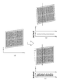
- FIGS. 5A to 5C are diagrams for explaining microarray images read by the scanner according to the present embodiment.
- FIG. 5A is a diagram illustrating an alignment image.
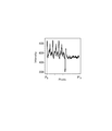
- FIG. 5B is a graph showing a change in light intensity between the arrows P-P ′ in the alignment image of FIG.
- FIG. 5C is a graph showing a difference in height of the DNA chip 100 between the arrows P-P ′ in the alignment image of FIG. From FIG. 5-2, it can be confirmed that the amount of reflected light is reduced at the position corresponding to the side surface of the recess 103 of the DNA chip 100, and the uneven shape on the substrate can be imaged. Based on this, the position of the concave portion 103 of the DNA chip 100 in the alignment image can be determined, and the fluorescent image can be aligned.
- a laser light source for example, wavelengths of 405 nm, 532 nm, and 635 nm
- a laser light source since it is parallel light, the edge (light intensity difference) can be clearly detected in the image data for alignment by the phenomenon described with reference to FIG.
- the excitation light cut filter 15b In general, a band-pass filter that transmits 550 to 600 nm is often used as the excitation light cut filter 15b for Cy3.
- the excitation light cut filter 15b generally uses light having a wavelength of excitation light of Cy5 ( 635 nm) is slightly transmitted (for example, the OD value of light of 635 nm is about 5), so that the uneven shape of the DNA chip 100 can be imaged as shown in FIG. That is, it is possible to receive the reflected light or scattered light from the surface of the substrate, not the fluorescence from the fluorescent molecules excited and emitted by the light of a specific wavelength, and image the uneven shape of the substrate itself.
- the DNA chip 100 When acquiring the alignment image data, it is preferable to place the DNA chip 100 closer to the objective lens 13 than the focal position.
- the focal position the height of the objective lens 13 is fixed, the DNA chip 100 is changed in the height direction (the optical axis direction of the objective lens 13), and the amount of fluorescence from each DNA probe is measured. It can be obtained by measuring the height.
- the height of the DNA chip 100 can be fixed and the height of the objective lens 13 can be raised or lowered.
- the position of the surface of the DNA chip 100 (imaging target surface) may be brought closer to the lens side by 100 ⁇ m or more from the focal position based on the relationship of ⁇ / f described above. preferable.
- the upper limit of the approaching distance is not particularly limited as long as the DNA chip 100 and the objective lens 13 do not collide, but in an apparatus such as the scanner 1, it is usually 3000 ⁇ m or less.
- the light source for acquiring the alignment image data it is preferable to use a light source that emits excitation light for exciting fluorescent molecules because the number of parts of the scanner can be reduced. It does not matter if it is provided.
- a method that does not use a filter when acquiring alignment image data can be adopted.
- the filter when the filter is not used, the amount of light entering the image acquisition unit becomes too large, which may damage the light detection mechanism of the image acquisition unit. Therefore, as described above, when irradiating laser light from the Cy5 laser light source 11, it is preferable to use a filter that slightly transmits the wavelength of the irradiating light source, such as using the excitation light cut filter 15b.
- the excitation light cut filter 15a may be used by irradiating laser light from the Cy3 laser light source 12.
- an ND filter is used in place of the excitation light cut filters 15a and 15b, or the laser light output itself is weakened without using the excitation light cut filters 15a and 15b and the ND filter, thereby obtaining alignment image data. It doesn't matter. Of course, combinations of these can also be applied.
- the substrate (DNA chip 100) was obtained from the focal position close to the 250 ⁇ m lens side.
- the image for alignment in which the edge shape of the substrate surface appears as shown in FIG. 5-1 by actively bringing the substrate closer to the lens side from the focal position and actively receiving the reflected light of the laser beam. Data is obtained.
- FIG. 6 is a flowchart showing image alignment processing according to the present embodiment.
- the DNA chip 100 is set in the scanner 1, and the fluorescence image data of the fluorescent dyes Cy5 and Cy3 is read by the image acquisition unit 17 as described above (step S101). Subsequently, while the DNA chip 100 is set, the laser light is irradiated from the Cy5 laser light source 11 and the excitation image cut filter 15b for Cy3 is used, and the image data for alignment is read by the image acquisition unit 17 (step) S102). At this time, as described above, the DNA chip 100 is disposed at a position closer to the objective lens 13 than the focal position. In step S102, the laser light from the laser light source 12 for Cy3 may be irradiated and the excitation light cut filter 15a for Cy5 may be used.
- step S103 the position of each DNA probe in the fluorescence image data is determined and analyzed using the alignment image data.
- At least three reference points in the alignment image data are detected (step S103).
- at least three reference points for example, as shown in FIG. 7, the coordinates of the four corners in the alignment image can be cited.
- Such a method of detecting the coordinates of the four corners is performed by the detection unit 20a, and includes the above-described position determination of the recess 103 by edge detection using light and dark information.
- regions Ea1 to Ea4 and Eb1 to Eb4 in which the outer edge of the recess 103 can be detected by the detection unit 20a are set in advance, and in each region, as shown in FIG. A change in light intensity between the arrows PP ′ is measured, and a difference in height of the DNA chip 100 is detected. Thereafter, the detection unit 20a linearly connects the center position of the region Ea1 and the center position of the region Ea2 using the center positions of the height differences detected in the regions Ea1 to Ea4 and Eb1 to Eb4. One side of the outer edge 103.
- the center position of the region Ea3 and the center position of the region Ea4 are respectively straight lines. Tie. Thereby, the outer edge of the recess 103 in the alignment image obtained by the image acquisition unit 17 is formed. Further, by obtaining the intersections (coordinates) of the straight lines formed by being connected to each other, the four corners of the recess 103 can be obtained as the reference points 110a to 110d.
- steps S104 and S105 the distortion of the fluorescence image data is corrected based on the reference point.
- the correction unit 20b detects, for example, the inclination angle ⁇ x with respect to the x-axis of each side of the outer edge of the recess 103 and the inclination angle ⁇ y with respect to the y-axis from the coordinates of the reference points 110a to 110d (step S104). ). It is desirable that the inclination angles ⁇ x and ⁇ y take an average value of the angles of the two line segments in the corresponding direction (facing) with respect to the four line segments connecting the coordinates of the four corners. Note that the inclination angles ⁇ x and ⁇ y can be calculated even when there are three reference points. Then, as shown in FIGS.
- the correction unit 20b uses the array angle ⁇ y of the side corresponding to the y-axis (the edge of the outer edge of the recess 103) with respect to the y-axis as the correction angle.
- the data is rotated so that the side corresponding to the y axis of the recess 103 is parallel to the y axis.
- the correction unit 20b uses the array angle ⁇ x of the side corresponding to the x axis (side of the outer edge of the recess 103) with respect to the x axis as a correction angle, and uses the fluorescent image.
- the data is rotated so that the side corresponding to the x-axis of the recess 103 is parallel to the x-axis.
- the correction unit 20b applies the above-described inclination angles ⁇ x and ⁇ y and the following formulas (1) and (2) to the spots 102 regularly arranged in the two directions detected as described above. Based on 2), conversion (shear deformation) is performed (step S105). Thereby, the shear deformation distortion of the image is corrected.
- (x, y) in the following formula (1) is coordinates before conversion
- (X, Y) is coordinates after conversion.
- ⁇ xy corresponding to the deviation of the scanning mechanism of the scanner is obtained by subtracting the inclination angle ⁇ y from the inclination angle ⁇ x as shown in the following formulas (1) and (2).
- the resin may expand due to moisture absorption or temperature change in the hybridization process or the washing process. Although it depends on the processing time in each process, it may expand several tens of ⁇ m, which affects the alignment accuracy.
- the correction unit 20b calculates the chip lengths in the x-axis direction and the y-axis direction from the coordinates of the four corners described above, and performs contraction / expansion correction on the fluorescence image data so as to match the design value. (Steps S106, S107).
- the determination unit 20c refers to the analysis definition file for the fluorescence image data subjected to the angle correction, the shear deformation correction, and the contraction / expansion correction by the correction unit 20b as described above. To do.
- the position information of each spot in the template stored in the analysis definition file in advance is, for example, the center coordinates of each spot with the upper left corner (reference point 110a) as the origin. Therefore, the determination unit 20c determines the position of each spot (probe) by calculating each spot frame with respect to the image after the shrinkage correction in step S107, for example, using the coordinates of the upper left corner as the origin, and FIG. Alignment as shown in 1 to 9-3 is performed (step S108).
- FIG. 9A is an image showing the result of alignment on the Cy3 fluorescence image data
- FIG. 9B is an image showing the result of alignment on the Cy5 fluorescence image data.
- a template (see FIG. 15) corresponding to each spot 102 can be applied to each spot 102 and associated with the detection area.
- FIG. 9-3 shows the result of alignment performed on alignment image data for confirmation.
- FIG. 9C it can be seen that the straight line portion at one corner of the outer edge of the recess 103 of the DNA chip 100 is orthogonal at the reference point 1101 by the alignment process.
- steps S101 and S102 and the order of steps S106 and S107 may be interchanged.
- the fluorescent image data obtained based on the hybridization of the DNA sample to the DNA probe in this way is processed to obtain desired numerical data.
- it is used to analyze the presence of a desired gene, whether or not a certain gene is expressed, and how much it is expressed.
- the image is corrected and aligned using the unevenness formed on the DNA chip 100. For this reason, the sample extracted from the specimen is arranged on the DNA chip 100 even for an image with a small amount of DNA probe that emits less DNA probes, and an image obtained by a reading device with poor scanning mechanism accuracy.
- the detection area positioning process can be executed with high accuracy.
- the image data for alignment is acquired at a position (surface position P2) where the imaging target surface of the DNA chip 100 is closer to the objective lens 13 than the focal position (surface position P0).
- An image capable of accurately detecting a difference in height of the substrate can be acquired.
- FIG. 10 shows another embodiment of an optical system suitable for the scanner used in the present invention.
- the scanner 2 shown in FIG. 10 uses the micro mirror 14a instead of the perforated mirror 14 of the scanner 1 so that the excitation light is reflected by the micro mirror 14a and is incident on the DNA chip 100. It has a function of geometrically separating the reflected light (detection light) of fluorescent light or excitation light and the regular reflected light so as not to guide the regular reflected light from the DNA chip 100 as noise to the image acquisition unit 17 side. Thereby, regular reflection light is separable from the optical path N3. Even in this configuration, the same effect as the scanner 1 described above can be obtained.
- the present invention is also applicable to a chip spotted with RNA, protein, minute sample, low molecular weight compound, cell, etc. Is possible.
- a similar method is used even when a protein (antibody) is immobilized instead of a DNA probe and the presence or absence of a reaction with a sample or quantification is detected by fluorescence.
- the protein present in the sample cell lysate is labeled with Cy5 and the protein present in the control cell lysate is labeled with Cy3 and the two are mixed and reacted with the antibody array, or the protein is labeled with biotin instead of fluorescently labeling.
- biotin instead of fluorescently labeling.
- RNA array this technique can be used when detecting hybridization of RNA immobilized on a substrate having a concavo-convex shape (spot 102) and fluorescently labeled DNA or RNA by fluorescence.
- spot 102 a concavo-convex shape
- the present invention can be applied when detecting a binding reaction between a micro sample or a cell immobilized on a substrate having an uneven shape and a fluorescent labeled specimen (for example, an antibody) by fluorescence. Is possible.
- a die corresponding to a substrate having a shape like the DNA chip 100 shown in FIG. 14 is manufactured by ultraprecision machining, and a substrate made of PMMA (polymethyl methacrylate) is formed by injection molding using this die. 100.
- the mold had a trace of cutting by the tool, and therefore, the tool cutting trace was transferred to the substrate.
- the substrate height disturbance due to the cutting trace was measured to be 1 ⁇ m or less.
- a DNA probe is fixed to the upper surface of the convex portion (spot 102) of the manufactured DNA chip 100, hybridization is performed, and a fluorescence image and an alignment image are obtained with a DNA chip scanner (3D-Gene Scanner (3D-Gene (registered trademark))).
- a DNA chip scanner (3D-Gene Scanner (3D-Gene (registered trademark))
- the apparatus configuration and conditions for acquiring the fluorescence image and the alignment image are as follows (1) to (4).
- the optical system of the scanner 1 shown in FIG. 1 was used as the optical system of the scanner. That is, it has a perforated mirror 14 for allowing laser light to enter the DNA chip 100 and allowing regular reflection light from the substrate to pass therethrough.
- the height of the DNA chip 100 (distance between the objective lens 13 and the DNA chip 100) was changed, and the height position where the fluorescence intensity was strongest was set to zero.
- This position is the focal position (surface position P0) of the laser beam.
- a laser having a wavelength of 635 nm and a bandpass filter for Cy5 were used.
- This scanner has a function that can adjust the distance between the substrate and the lens.
- a laser (wavelength 635 nm) for measuring the fluorescence of Cy5 was used, and the same filter as the bandpass filter used when measuring Cy3 was used.
- the filter for Cy3 used in this example has an OD value of about 5 at 635 nm, and transmits a wavelength of 635 nm.
- the offset position (distance from the focal position to the substrate surface) was changed from ⁇ 500 ⁇ m to +1500 ⁇ m, and the images of reflected and scattered light were compared (FIG. 3).
- the expression that the offset position is 0 indicates that the substrate is at the focal position (surface position P0) of the laser beam focused by the objective lens.
- the sign of the offset position is negative, the substrate is at a position far away from the objective lens (surface position P1) with reference to the focal position.
- the sign is positive, the substrate is close to the objective lens with reference to the focal position. It shows that it exists in a position (surface position P2).
- FIG. 11 is an image (A) of the DNA chip 100 (substrate) read by the scanner 1 according to the example of the present invention and a graph (B) of the light intensity change.
- FIG. 11A is a graph showing an image when the offset position is 0 and a change in light intensity between the arrows P 1 -P 1 ′ in the image.
- FIGS. 11-2 to 11-9 illustrate images when the offset positions are +100, +200, +300, +400, +500, +750, +1000, and +1500, and an arrow P 3 between the arrows P 2 and P 2 ′ in the image.
- FIGS. 11-10 to 11-12 show images when the offset positions are ⁇ 100, ⁇ 200, and ⁇ 500, and arrows P 10 to P 10 ′, arrows P 11 to P 11 ′, and arrows in the image. it is a graph showing the light intensity change between P 12 -P 12 '. Note that the image shown in FIG. 11 is an image corresponding to the alignment image data corrected by the correction unit 20b described above.
- the offset position when acquiring the alignment image is changed to ⁇ 500 ⁇ m, 0 ⁇ m, +100 ⁇ m, +200 ⁇ m, +500 ⁇ m, +1000 ⁇ m, +1250 ⁇ m, and +1500 ⁇ m to determine whether the image alignment processing can be performed appropriately.
- the evaluation was performed by the following procedures (1) ′ to (5) ′.
- a total of 20 DNA chips that had been subjected to the hybridization treatment were prepared.
- the shape of the DNA chip substrate is as shown in FIG.
- the difference in height between the edge portions is 90 ⁇ m, and the angle ⁇ shown in FIG. 4A is 70 degrees.
- the offset position was set to ⁇ 100 ⁇ m, 0 ⁇ m, +100 ⁇ m, +200 ⁇ m, +500 ⁇ m, +750 ⁇ m, +1000 ⁇ m, +1250 ⁇ m, and +1500 ⁇ m, and alignment images were obtained at each position.
- a laser wavelength 635 nm
- the same filter as the band-pass filter used when measuring Cy3 was used.
- Reference points corresponding to the reference points 110a to 110d in FIG. 7 were detected by an edge detection method using light / dark information based on the respective alignment image data.
- the alignment reliability is clearly increased by bringing the DNA chip closer to the objective lens with respect to the focal position when acquiring the alignment image.
- the reliability is greatly increased by setting the substrate closer to the +200 ⁇ m objective lens side than the focal position when acquiring the alignment image.
- the f value of the objective lens mounted on the scanner 1 according to this example was 6.0 mm. Therefore, from the above results, when the offset position ( ⁇ ) is in the range of +100 to +1000, the preferable range of ⁇ / f is in the range of 0.017 (100/6000) to 0.17 (1000/6000). . In this range, the success probability is 95% or more. More preferably, the offset position is in the range of +200 to +1000, and the range of ⁇ / f is 0.033 (200/6000) to 0.17 (1000/6000). Within this range, the success probability of alignment is 100%.
- FIGS. 12-1 to 12-3 are graphs of an image and fluorescence intensity of the slide glass according to this example.
- FIG. 12A is an image obtained by the scanner 1.
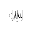
- FIG. 12-2 is a graph showing a change in light intensity between arrows P 13 and P 13 ′ in the image of FIG. 12-1.
- FIG. 12-3 is a graph showing a difference in height on the slide glass between arrows P 13 and P 13 ′ in the image of FIG. 12-1.
- the detection method, the microarray analysis method, and the fluorescence reading apparatus according to the present invention are suitable for acquiring an image capable of accurately detecting a difference in substrate height and appropriately performing alignment processing.
Landscapes
- Health & Medical Sciences (AREA)
- Physics & Mathematics (AREA)
- General Physics & Mathematics (AREA)
- Life Sciences & Earth Sciences (AREA)
- Engineering & Computer Science (AREA)
- Immunology (AREA)
- Chemical & Material Sciences (AREA)
- Analytical Chemistry (AREA)
- Biochemistry (AREA)
- General Health & Medical Sciences (AREA)
- Nuclear Medicine, Radiotherapy & Molecular Imaging (AREA)
- Pathology (AREA)
- Data Mining & Analysis (AREA)
- Theoretical Computer Science (AREA)
- Mathematical Physics (AREA)
- Molecular Biology (AREA)
- Biomedical Technology (AREA)
- Computational Mathematics (AREA)
- Mathematical Analysis (AREA)
- Mathematical Optimization (AREA)
- Algebra (AREA)
- Pure & Applied Mathematics (AREA)
- Databases & Information Systems (AREA)
- Software Systems (AREA)
- General Engineering & Computer Science (AREA)
- Investigating, Analyzing Materials By Fluorescence Or Luminescence (AREA)
- Length Measuring Devices By Optical Means (AREA)
Abstract
Description


平らなスライドガラスの上に厚さ150μmのテープをはり、それを上記のスキャナー1にセットした。オフセット量+250μmの状態で、Cy5の蛍光を測定するレーザー(波長635nm)を使用し、フィルタとしてはCy3を測定する際に使用するバンドパスフィルタと同じものを用いて、アライメント用画像に相当する画像データを得た。この条件は図4-1で示す角度θが90度に相当する。その結果を図12-1~12-3に示す。
11,12 レーザー光源
13 対物レンズ
14 穴あきミラー
14a 微小ミラー
15 カットフィルタ
15a,15b 励起光カットフィルタ
16 結像レンズ
17 画像取得部
18,19 ミラー
20 制御部
20a 検出部
20b 補正部
20c 決定部
21 駆動部
100 DNAチップ
101 ブロック
102 スポット
103 凹部
104 保持部
140 穴
Claims (10)
- レンズによって集光されたレーザー光を、凹凸形状を有する基板に照射し、該基板からの反射光および/または散乱光の光強度を画像データとして取得して前記凹凸形状の高さの差異を検出する検出方法であって、
前記レンズの焦点位置よりも前記レンズに近い位置に前記基板の光照射面を配置し、該光照射面からの反射光および/または散乱光を検出光として受光し、該受光した光の強度の変化に基いて前記基板の高さの差異を検出することを特徴とする検出方法。 - 前記基板の光照射面を前記焦点位置に配置した場合に、該光照射面からの正反射光を前記検出光から分離する光学系を用いることを特徴とする請求項1に記載の検出方法。
- 前記レンズの焦点距離をf、前記基板を前記焦点位置から前記レンズに近づける距離をαとしたとき、α/fが所定の範囲内となるように設定されるαに応じた位置に前記基板の光照射面を配置することを特徴とする請求項1または2に記載の検出方法。
- 凹凸形状が形成され、各々蛍光標識されたサンプルと結合可能な複数のプローブが配置されたマイクロアレイに対し、対物レンズを介して前記蛍光標識の励起波長を含む光を照射し、かつ前記マイクロアレイからの光を受光して、該受光した光に基づく画像をもとに前記マイクロアレイの解析を行うマイクロアレイの解析方法であって、
前記蛍光標識からの蛍光を検出して蛍光画像データを取得する蛍光画像データ取得ステップと、
前記マイクロアレイの表面からの光を検出して、前記蛍光画像データのアライメントを行うアライメント用画像データを取得するアライメント用画像データ取得ステップと、
前記アライメント用画像データの光強度の変化をもとに、前記凹凸形状の高さの差異を検出する検出ステップと、
前記検出ステップによって検出された前記凹凸形状の高さの差異に基づいて前記蛍光画像データを補正する補正ステップと、
前記補正ステップによって補正された前記蛍光画像データにおける各プローブの位置を決定する位置決定ステップと、
を含み、
前記アライメント用画像データ取得ステップは、前記マイクロアレイの表面を、前記対物レンズの焦点位置に対して該対物レンズに近い位置に配置した状態で、前記アライメント用画像データを取得することを特徴とするマイクロアレイの解析方法。 - 前記検出ステップは、前記アライメント用画像データにおいて、前記光強度の変化に基づいて3つ以上の基準点を検出し、
前記補正ステップは、検出した基準点を基に前記蛍光画像データの歪みを補正することを特徴とする請求項4に記載のマイクロアレイの解析方法。 - 前記補正ステップは、前記基準点に基づく前記アライメント用画像データの傾斜角度θx,θyを取得して、該傾斜角度θx,θyおよび下記式(1),(2)をもとに、前記蛍光画像データの剪断変形歪みを補正することを特徴とする請求項5に記載のマイクロアレイの解析方法。

- 前記アライメント用画像データ取得ステップは、前記対物レンズの焦点距離をf、前記マイクロアレイを前記焦点位置から前記対物レンズに近づける距離をαとしたとき、α/fが所定の範囲内となるように設定されるαに応じた位置に前記マイクロアレイの表面を配置して前記アライメント用画像データを取得することを特徴とする請求項4~6のいずれか一つに記載のマイクロアレイの解析方法。
- 前記マイクロアレイは、DNAマイクロアレイであることを特徴とする請求項4~7のいずれか一つに記載のマイクロアレイの解析方法。
- 凹凸形状が形成され、各々蛍光標識されたサンプルと結合可能な複数のプローブが配置された基板から、前記蛍光標識の蛍光を含む光を受光して、該受光した光に基づく画像データを取得する蛍光読取装置であって、
少なくとも所定波長の励起光を含む照明光を出射する光源と、
前記照明光を前記基板に照射するとともに、該照明光が照射された前記基板の表面からの光を受光する対物レンズと、
前記対物レンズが受光した光を検出して、該検出した蛍光による蛍光画像データおよび前記基板からの光による基板画像データを取得する画像取得部と、
画像取得部によって取得された前記基板画像データをもとに、前記凹凸形状の高さの差異を検出する検出部と、
前記検出部によって検出された前記凹凸形状の高さの差異をもとに、前記蛍光画像データを補正する補正部と、
前記基板を保持する保持手段と、
前記保持手段を前記対物レンズの光軸に沿って移動させる駆動部と、
を備え、
前記駆動部は、前記画像取得部により前記基板画像データを取得する際、前記対物レンズの焦点位置に対して、前記対物レンズに近い位置に前記基板を配置するように前記保持手段を移動させることを特徴とする蛍光読取装置。 - 前記駆動部は、前記対物レンズの焦点距離をf、前記基板を前記焦点位置から前記対物レンズに近づける距離をαとしたとき、α/fが所定の範囲内となるように設定されるαに応じた位置に前記基板を配置するように前記保持手段を移動させることを特徴とする請求項9に記載の蛍光読取装置。
Priority Applications (5)
| Application Number | Priority Date | Filing Date | Title |
|---|---|---|---|
| EP13845775.9A EP2908089B1 (en) | 2012-10-12 | 2013-10-04 | Height difference detection method, microarray analysis method and fluorescence reading device |
| KR1020157008883A KR102136648B1 (ko) | 2012-10-12 | 2013-10-04 | 검출 방법, 마이크로어레이의 해석 방법 및 형광 판독 장치 |
| US14/433,972 US9823197B2 (en) | 2012-10-12 | 2013-10-04 | Detecting method, microarray analyzing method, and fluorescence reading device |
| CN201380052862.2A CN104718427B (zh) | 2012-10-12 | 2013-10-04 | 检测方法、微阵列的分析方法及荧光读取装置 |
| JP2013546519A JP6291842B2 (ja) | 2012-10-12 | 2013-10-04 | 検出方法、マイクロアレイの解析方法および蛍光読取装置 |
Applications Claiming Priority (2)
| Application Number | Priority Date | Filing Date | Title |
|---|---|---|---|
| JP2012-227302 | 2012-10-12 | ||
| JP2012227302 | 2012-10-12 |
Publications (1)
| Publication Number | Publication Date |
|---|---|
| WO2014057893A1 true WO2014057893A1 (ja) | 2014-04-17 |
Family
ID=50477360
Family Applications (1)
| Application Number | Title | Priority Date | Filing Date |
|---|---|---|---|
| PCT/JP2013/077159 Ceased WO2014057893A1 (ja) | 2012-10-12 | 2013-10-04 | 検出方法、マイクロアレイの解析方法および蛍光読取装置 |
Country Status (6)
| Country | Link |
|---|---|
| US (1) | US9823197B2 (ja) |
| EP (1) | EP2908089B1 (ja) |
| JP (1) | JP6291842B2 (ja) |
| KR (1) | KR102136648B1 (ja) |
| CN (1) | CN104718427B (ja) |
| WO (1) | WO2014057893A1 (ja) |
Cited By (2)
| Publication number | Priority date | Publication date | Assignee | Title |
|---|---|---|---|---|
| JP2017102013A (ja) * | 2015-12-01 | 2017-06-08 | キヤノン株式会社 | 走査型顕微鏡 |
| JP2017102266A (ja) * | 2015-12-01 | 2017-06-08 | キヤノン株式会社 | 走査型顕微鏡 |
Families Citing this family (13)
| Publication number | Priority date | Publication date | Assignee | Title |
|---|---|---|---|---|
| KR102459817B1 (ko) | 2015-10-01 | 2022-10-27 | 삼성디스플레이 주식회사 | 레이저 결정화 장치 |
| GB201701688D0 (en) | 2017-02-01 | 2017-03-15 | Illumia Inc | System and method with fiducials in non-recliner layouts |
| GB201701689D0 (en) | 2017-02-01 | 2017-03-15 | Illumia Inc | System and method with fiducials of non-closed shapes |
| GB201701686D0 (en) | 2017-02-01 | 2017-03-15 | Illunina Inc | System & method with fiducials having offset layouts |
| GB201701691D0 (en) * | 2017-02-01 | 2017-03-15 | Illumina Inc | System and method with reflective fiducials |
| CN109414673B (zh) | 2017-02-01 | 2021-09-07 | 伊鲁米那股份有限公司 | 具有响应于多个激发频率的基准的系统和方法 |
| CN107723344B (zh) * | 2017-09-05 | 2020-12-08 | 西北工业大学 | 基于dPCR的新型全自动荧光信号采集分析方法 |
| CN108181478B (zh) * | 2017-12-19 | 2021-01-05 | 西北工业大学 | 一种阵列式微流控芯片的荧光采集分析方法 |
| CN111351721A (zh) * | 2020-03-31 | 2020-06-30 | 中国电建集团北京勘测设计研究院有限公司 | 测定原位剪切试验中实际剪切破坏面起伏差的测量仪及其测量方法 |
| CN111879782B (zh) * | 2020-06-30 | 2023-10-03 | 深圳中科飞测科技股份有限公司 | 检测装置及检测方法 |
| DE102021204401A1 (de) | 2021-05-03 | 2022-11-03 | Robert Bosch Gesellschaft mit beschränkter Haftung | Verfahren zum Auslesen eines insbesondere biologischen Arrays und Prozessierungseinrichtung |
| CN114136243B (zh) * | 2021-10-18 | 2024-08-02 | 广州国显科技有限公司 | 一种应用于测量显示面板展平度的装置 |
| EP4616195A1 (en) * | 2022-11-08 | 2025-09-17 | Zhong Li | Methods for detecting target compounds and uses thereof |
Citations (6)
| Publication number | Priority date | Publication date | Assignee | Title |
|---|---|---|---|---|
| JP2003148925A (ja) * | 2001-11-12 | 2003-05-21 | Lasertec Corp | 深さ測定装置及び膜厚測定装置 |
| JP2005024532A (ja) | 2003-06-13 | 2005-01-27 | Institute Of Physical & Chemical Research | 生体分子マイクロアレイ用基板、生体分子マイクロアレイ、相互作用促進用装置および方法、ならびに、相互作用の検出方法 |
| JP2005049282A (ja) * | 2003-07-30 | 2005-02-24 | Hamamatsu Photonics Kk | 蛍光観察装置及びレーザ光照射装置 |
| JP2005172840A (ja) | 2002-02-14 | 2005-06-30 | Ngk Insulators Ltd | 試料解析装置および試料解析方法 |
| WO2012101943A1 (ja) * | 2011-01-28 | 2012-08-02 | 東レ株式会社 | マイクロアレイの解析方法および読取り装置 |
| JP2013224894A (ja) * | 2012-04-23 | 2013-10-31 | Toray Ind Inc | マイクロアレイの解析方法 |
Family Cites Families (4)
| Publication number | Priority date | Publication date | Assignee | Title |
|---|---|---|---|---|
| US20030152255A1 (en) | 2002-02-14 | 2003-08-14 | Ngk Insulators, Ltd. | Probe reactive chip, apparatus for analyzing sample and method thereof |
| US7200254B2 (en) | 2002-02-14 | 2007-04-03 | Ngk Insulators, Ltd. | Probe reactive chip, sample analysis apparatus, and method thereof |
| KR100622243B1 (ko) | 2004-02-17 | 2006-09-14 | 오므론 가부시키가이샤 | 광학식 측정 장치 및 광학식 측정 방법 |
| KR101513602B1 (ko) | 2009-02-11 | 2015-04-22 | 삼성전자주식회사 | 바이오칩 스캐닝 방법 |
-
2013
- 2013-10-04 JP JP2013546519A patent/JP6291842B2/ja active Active
- 2013-10-04 CN CN201380052862.2A patent/CN104718427B/zh active Active
- 2013-10-04 WO PCT/JP2013/077159 patent/WO2014057893A1/ja not_active Ceased
- 2013-10-04 KR KR1020157008883A patent/KR102136648B1/ko active Active
- 2013-10-04 US US14/433,972 patent/US9823197B2/en active Active
- 2013-10-04 EP EP13845775.9A patent/EP2908089B1/en active Active
Patent Citations (6)
| Publication number | Priority date | Publication date | Assignee | Title |
|---|---|---|---|---|
| JP2003148925A (ja) * | 2001-11-12 | 2003-05-21 | Lasertec Corp | 深さ測定装置及び膜厚測定装置 |
| JP2005172840A (ja) | 2002-02-14 | 2005-06-30 | Ngk Insulators Ltd | 試料解析装置および試料解析方法 |
| JP2005024532A (ja) | 2003-06-13 | 2005-01-27 | Institute Of Physical & Chemical Research | 生体分子マイクロアレイ用基板、生体分子マイクロアレイ、相互作用促進用装置および方法、ならびに、相互作用の検出方法 |
| JP2005049282A (ja) * | 2003-07-30 | 2005-02-24 | Hamamatsu Photonics Kk | 蛍光観察装置及びレーザ光照射装置 |
| WO2012101943A1 (ja) * | 2011-01-28 | 2012-08-02 | 東レ株式会社 | マイクロアレイの解析方法および読取り装置 |
| JP2013224894A (ja) * | 2012-04-23 | 2013-10-31 | Toray Ind Inc | マイクロアレイの解析方法 |
Non-Patent Citations (1)
| Title |
|---|
| See also references of EP2908089A4 |
Cited By (3)
| Publication number | Priority date | Publication date | Assignee | Title |
|---|---|---|---|---|
| JP2017102013A (ja) * | 2015-12-01 | 2017-06-08 | キヤノン株式会社 | 走査型顕微鏡 |
| JP2017102266A (ja) * | 2015-12-01 | 2017-06-08 | キヤノン株式会社 | 走査型顕微鏡 |
| US10845583B2 (en) | 2015-12-01 | 2020-11-24 | Canon Kabushiki Kaisha | Scanning microscope |
Also Published As
| Publication number | Publication date |
|---|---|
| EP2908089A4 (en) | 2016-06-08 |
| CN104718427B (zh) | 2018-01-30 |
| CN104718427A (zh) | 2015-06-17 |
| EP2908089A1 (en) | 2015-08-19 |
| US20150276604A1 (en) | 2015-10-01 |
| US9823197B2 (en) | 2017-11-21 |
| JP6291842B2 (ja) | 2018-03-14 |
| JPWO2014057893A1 (ja) | 2016-09-05 |
| EP2908089B1 (en) | 2022-04-13 |
| KR102136648B1 (ko) | 2020-07-22 |
| KR20150064067A (ko) | 2015-06-10 |
Similar Documents
| Publication | Publication Date | Title |
|---|---|---|
| JP6291842B2 (ja) | 検出方法、マイクロアレイの解析方法および蛍光読取装置 | |
| JP5817378B2 (ja) | マイクロアレイの解析方法および読取り装置 | |
| US20250377527A1 (en) | Methods and systems for multidimensional imaging | |
| ES2407968T3 (es) | Procedimientos y aparatos para la formación confocal de imágenes | |
| US8023162B2 (en) | Hexagonal site line scanning method and system | |
| US8867029B2 (en) | Systems for and methods of facilitating focusing an optical scanner | |
| JPWO2007091530A1 (ja) | 光検出装置及び測定対象読取装置 | |
| US20080117518A1 (en) | Microarray line scanning method and system | |
| US7173701B2 (en) | CCD-based biochip reader | |
| US20110081098A1 (en) | Method of correcting distortion of scanned image | |
| JP2013224894A (ja) | マイクロアレイの解析方法 | |
| JP2004184379A (ja) | マイクロアレイの読取方法 | |
| KR101188233B1 (ko) | 바이오칩을 위한 진단장치 | |
| US20240100518A1 (en) | Flow cell based motion system calibration and control methods | |
| WO2025059293A1 (en) | Methods and compositions for assessing the performance of instruments adapted for single-molecule tracking |
Legal Events
| Date | Code | Title | Description |
|---|---|---|---|
| ENP | Entry into the national phase |
Ref document number: 2013546519 Country of ref document: JP Kind code of ref document: A |
|
| 121 | Ep: the epo has been informed by wipo that ep was designated in this application |
Ref document number: 13845775 Country of ref document: EP Kind code of ref document: A1 |
|
| ENP | Entry into the national phase |
Ref document number: 20157008883 Country of ref document: KR Kind code of ref document: A |
|
| WWE | Wipo information: entry into national phase |
Ref document number: 14433972 Country of ref document: US |
|
| WWE | Wipo information: entry into national phase |
Ref document number: 2013845775 Country of ref document: EP |
|
| NENP | Non-entry into the national phase |
Ref country code: DE |