WO2014069306A1 - 基板及び金属層の製造方法 - Google Patents
基板及び金属層の製造方法 Download PDFInfo
- Publication number
- WO2014069306A1 WO2014069306A1 PCT/JP2013/078712 JP2013078712W WO2014069306A1 WO 2014069306 A1 WO2014069306 A1 WO 2014069306A1 JP 2013078712 W JP2013078712 W JP 2013078712W WO 2014069306 A1 WO2014069306 A1 WO 2014069306A1
- Authority
- WO
- WIPO (PCT)
- Prior art keywords
- outer peripheral
- metal layer
- peripheral portion
- bent
- bent portion
- Prior art date
- Legal status (The legal status is an assumption and is not a legal conclusion. Google has not performed a legal analysis and makes no representation as to the accuracy of the status listed.)
- Ceased
Links
Images


Classifications
-
- H—ELECTRICITY
- H05—ELECTRIC TECHNIQUES NOT OTHERWISE PROVIDED FOR
- H05K—PRINTED CIRCUITS; CASINGS OR CONSTRUCTIONAL DETAILS OF ELECTRIC APPARATUS; MANUFACTURE OF ASSEMBLAGES OF ELECTRICAL COMPONENTS
- H05K1/00—Printed circuits
- H05K1/02—Details
- H05K1/11—Printed elements for providing electric connections to or between printed circuits
- H05K1/115—Via connections; Lands around holes or via connections
-
- H—ELECTRICITY
- H05—ELECTRIC TECHNIQUES NOT OTHERWISE PROVIDED FOR
- H05K—PRINTED CIRCUITS; CASINGS OR CONSTRUCTIONAL DETAILS OF ELECTRIC APPARATUS; MANUFACTURE OF ASSEMBLAGES OF ELECTRICAL COMPONENTS
- H05K1/00—Printed circuits
- H05K1/02—Details
- H05K1/0201—Thermal arrangements, e.g. for cooling, heating or preventing overheating
- H05K1/0203—Cooling of mounted components
- H05K1/0204—Cooling of mounted components using means for thermal conduction connection in the thickness direction of the substrate
- H05K1/0206—Cooling of mounted components using means for thermal conduction connection in the thickness direction of the substrate by printed thermal vias
-
- H—ELECTRICITY
- H05—ELECTRIC TECHNIQUES NOT OTHERWISE PROVIDED FOR
- H05K—PRINTED CIRCUITS; CASINGS OR CONSTRUCTIONAL DETAILS OF ELECTRIC APPARATUS; MANUFACTURE OF ASSEMBLAGES OF ELECTRICAL COMPONENTS
- H05K3/00—Apparatus or processes for manufacturing printed circuits
- H05K3/40—Forming printed elements for providing electric connections to or between printed circuits
- H05K3/4038—Through-connections; Vertical interconnect access [VIA] connections
- H05K3/4084—Through-connections; Vertical interconnect access [VIA] connections by deforming at least one of the conductive layers
-
- H—ELECTRICITY
- H05—ELECTRIC TECHNIQUES NOT OTHERWISE PROVIDED FOR
- H05K—PRINTED CIRCUITS; CASINGS OR CONSTRUCTIONAL DETAILS OF ELECTRIC APPARATUS; MANUFACTURE OF ASSEMBLAGES OF ELECTRICAL COMPONENTS
- H05K1/00—Printed circuits
- H05K1/02—Details
- H05K1/0201—Thermal arrangements, e.g. for cooling, heating or preventing overheating
- H05K1/0203—Cooling of mounted components
- H05K1/0209—External configuration of printed circuit board adapted for heat dissipation, e.g. lay-out of conductors, coatings
-
- H—ELECTRICITY
- H05—ELECTRIC TECHNIQUES NOT OTHERWISE PROVIDED FOR
- H05K—PRINTED CIRCUITS; CASINGS OR CONSTRUCTIONAL DETAILS OF ELECTRIC APPARATUS; MANUFACTURE OF ASSEMBLAGES OF ELECTRICAL COMPONENTS
- H05K1/00—Printed circuits
- H05K1/02—Details
- H05K1/11—Printed elements for providing electric connections to or between printed circuits
- H05K1/111—Pads for surface mounting, e.g. lay-out
- H05K1/112—Pads for surface mounting, e.g. lay-out directly combined with via connections
-
- H—ELECTRICITY
- H05—ELECTRIC TECHNIQUES NOT OTHERWISE PROVIDED FOR
- H05K—PRINTED CIRCUITS; CASINGS OR CONSTRUCTIONAL DETAILS OF ELECTRIC APPARATUS; MANUFACTURE OF ASSEMBLAGES OF ELECTRICAL COMPONENTS
- H05K2201/00—Indexing scheme relating to printed circuits covered by H05K1/00
- H05K2201/06—Thermal details
- H05K2201/066—Heatsink mounted on the surface of the printed circuit board [PCB]
Definitions
- the technology of the present disclosure relates to a substrate in which a metal layer made of a metal plate is adhered to an insulating substrate, and a method of manufacturing a metal layer used for the substrate.
- Patent Document 1 discloses a substrate in which a metal layer formed by punching a metal plate in a predetermined pattern shape is bonded to one surface of an insulating substrate.
- the metal layer made of a metal plate can be bent to change its shape. Therefore, a bending portion formed by bending a part of the metal layer is provided in a metal layer made of a metal plate, and a function is added to the metal layer using the bending portion.
- an end portion of a metal layer is bent to form a bent portion rising from an insulating substrate, and the bent portion is used as a connection terminal to an external circuit.
- providing various bent portions in the metal layer is also performed depending on the shape and the like of the insulating substrate to which the metal layer is adhered.
- the bent portion is formed by bending a metal plate punched into a predetermined pattern shape into a predetermined three-dimensional shape by press molding. At this time, depending on the shape of the bent portion, a crease may be formed in the peripheral portion of the bent portion. For example, in the case where a bent portion which bulges in the thickness direction of the metal layer is formed at the central portion of the metal layer, the peripheral portion of the bent portion is moved toward the bent portion by the amount of pushing the bent portion in the thickness direction. As a result, distortion occurs in the peripheral portion of the bent portion to form wrinkles in the metal layer. Then, if a wrinkle is formed in the metal layer, when the metal layer is bonded to the insulating substrate, a gap may be generated between the metal layer and the insulating substrate, and the adhesion strength of the substrate may be reduced.
- An object of the present disclosure is to preferably bond a metal layer and an insulating substrate by suppressing the formation of wrinkles on the metal layer in a substrate formed of a metal plate and having a metal layer having a bent portion bonded to the insulating substrate. It is to let
- a substrate for achieving the above object comprises an insulating substrate having a first surface and a second surface, and a metal layer made of a metal plate and bonded to the first surface.
- the insulating substrate has a through hole.
- the metal layer is disposed in a bent portion inserted into the through hole and expanding in a direction from the first surface toward the second surface, and is positioned around the same bent portion and bonded to the first surface And an outer peripheral portion.
- the bend has opposite first and second ends and is bent relative to the outer circumference at the first and second ends.
- the outer circumferential portion is divided into a first outer circumferential portion continuous with the first end of the bent portion and a second outer circumferential portion continuous with the second end of the bent portion.
- a method of manufacturing a metal layer for achieving the above object is a method of manufacturing a metal layer having a bent portion which bulges in a bridge shape, and a bend forming portion which is a portion to be the bend later and the bend formation
- the primary forming is performed by punching out a predetermined pattern shape from a metal plate and using a mold having an inner surface shape corresponding to the bent portion. And press-molding an article. The punching forms two parallel first notches in the primary molded product, thereby forming the bend with the first end and the second end opposite to each other in the direction in which the first notches extend.
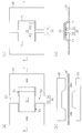
- the bottom view of the substrate of an embodiment. (A) is a top view of the primary molded product, (b) is a cross-sectional view of the primary molded product, (c) is a top view of the lower metal layer, and (d) is a cross-sectional view of the lower metal layer.
- the substrate 10 is provided with an insulating substrate 11 in which a rectangular through hole 12 is formed at the center.
- a flat plate-like upper metal layer 20 made of a metal plate and having a predetermined pattern shape is adhered to the upper surface (second surface) of the insulating substrate 11.
- a rectangular through hole 21 slightly larger than the through hole 12 is formed in a portion of the upper metal layer 20 corresponding to the through hole 12 of the insulating substrate 11.
- a lower metal layer 30 having a predetermined pattern shape and made of a metal plate is adhered on the lower surface (first surface) of the insulating substrate 11.
- the lower metal layer 30 is formed of a single metal plate, and includes a bending portion 31 located at the center thereof and an outer peripheral portion 32 continuous with the first and second ends of the bending portion. There is.
- the bent portion 31 functions as a mounting portion for mounting a heat generating element 40 described later, has a bridge shape that bulges upward, and is provided with a flat portion 31 a having a square shape in top view.
- the bending portion 31 bends a part of the lower metal layer 30. Specifically, the bending portion 31 bends upward (valley fold) at a first fold line P1 and lower side (peak fold) at a second fold line P2. It is formed by bending into.
- the first bending line P1 corresponds to both ends of the bending portion 31, that is, the first end and the second end.
- the bent portion 31 overlaps the through hole 12 of the insulating substrate 11 and the through hole 21 of the upper metal layer 20 when viewed from the thickness direction of the substrate 10.
- the bent portion 31 is inserted into the through holes 12 and 21 from the lower surface of the insulating substrate 11 to expose the plane portion 31 a from the upper surface of the insulating substrate 11.
- the upper surface of the flat portion 31 a of the bent portion 31 is located on the same plane as the upper surface of the upper metal layer 20. That is, the height of the upper surface of the flat portion 31 a and the upper metal layer 20 are set by setting the amount of expansion of the bent portion 31 to a value corresponding to the total value of the thickness of the insulating substrate 11 and the thickness of the upper metal layer 20. Align with the height of the top of the
- the outer peripheral portion 32 functions as a bonding portion for bonding the lower metal layer 30 to the insulating substrate 11 and a heat radiating portion for diffusing and radiating the heat transmitted to the bending portion 31.
- the outer peripheral portion 32 has a first outer peripheral portion 33 continuous with the first end (P1) of the bent portion 31 and a second outer peripheral portion 34 continuous with the second end (P2) of the bent portion 31. And divided into That is, the first outer peripheral portion 33 and the second outer peripheral portion 34 are connected to each other only through the bending portion 31.
- the first outer peripheral portion 33 is continuous with the first end of the bending portion 31, and is continuous with the side portion 33a located to the side of the bending portion 31, and the side portion 33a, and is more than the first bending line P1. It extends inward and has an extending portion 33 b located in front of and behind the bent portion 31.
- the second outer peripheral portion 34 is continuous with the second end of the bending portion 31, and is continuous with the side portion 34a and the side portion 34a located on the side of the bending portion 31, and also the first bending curve It has an extending portion 34 b which extends inward of P 1 and is located in front of and behind the bent portion 31.
- the positional relationship between the bending portion 31 and the first folding line P1 is the side
- the positional relationship between the bending section 31 and the first bending line P1 is the front and back. .
- the portion adjacent to the bending portion 31 in plan view coincides with the periphery of the through hole 12 of the insulating substrate 11. Further, at each end portion of the opposing extending portions 33b and 34b, two sides opposing each other with a gap S are provided. The first outer peripheral portion 33 and the second outer peripheral portion 34 are divided by the gap S.
- the outer shape of the entire outer peripheral portion 32 is substantially the same as the outer shape of the upper metal layer 20.
- the upper metal layer 20 and the lower metal layer 30 are straddled on the upper surface of the upper metal layer 20 and the upper surface of the flat portion 31 a of the bent portion 31 in the lower metal layer 30.
- the heating element 40 is joined.
- the heat dissipation member 41 is joined to the lower surface of the lower metal layer 30.
- the heat radiating member 41 has a projecting portion, and the projecting portion is joined to the lower surface of the flat portion 31 a of the bending portion 31.
- a flat plate-shaped primary molded product 30 'shown in FIG. 4A is formed by punching out a predetermined pattern shape from a metal plate with a press. At this time, two parallel first notches 51 extending in the lateral direction are formed in the central portion of the primary molded product 30 '. Thus, a bend forming portion 31 ′ which is a portion to be the bending portion 31 later is formed between the two first notches 51.
- a second cut 52 extending in the longitudinal direction from the central portion of the first cut 51 is formed in the primary molded product 30 ′.
- the outer peripheral portion 32 located around the bend forming portion 31 ′ is a first outer peripheral portion 33 continuous with the first end of the bend forming portion 31 ′ by the second cut 52, and a second outer peripheral portion continuous with the second end It is divided into 34 and.
- the width of the second cut 52 is set to a value larger than the amount of expansion of the bent portion 31, that is, the total value of the thicknesses of the insulating substrate 11 and the upper metal layer 20.
- the primary molded article 30 ′ is press-molded by a mold 60 having an inner surface shape corresponding to the bending portion 31.
- the bend forming portion 31 ' is bent in a bridge shape at the dashed dotted line portion shown in FIG. 4A to form the bent portion 31, and from the primary formed product 30' to FIG. 4C and FIG.
- the lower metal layer 30 shown is molded.
- a force that pulls inward along the first cut 51 acts on the outer peripheral portion 32 of the primary molded product 30 ′.
- the outer peripheral portion 32 is divided into the first outer peripheral portion 33 and the second outer peripheral portion 34 by the second cut 52. Therefore, the outer peripheral portion 32 moves only in the direction in which the first outer peripheral portion 33 and the second outer peripheral portion 34 approach each other, and distortion due to the pulling force does not occur in the outer peripheral portion 32. Therefore, the formation of a ridge on the outer peripheral portion 32 of the lower metal layer 30 is suppressed.
- the lower metal layer 30 manufactured as described above is disposed on the lower surface of the insulating substrate 11 such that the bent portion 31 is inserted into the through hole 12 of the insulating substrate 11, and the lower surface of the insulating substrate 11 at the outer peripheral portion 32. Glued to.
- the outer peripheral portion 32 bonded to the insulating substrate 11 is a first outer peripheral portion 33 continuous with the first end of the bent portion 31 and a second outer peripheral portion connected with the second end of the bent portion 31. It is divided into 34 and. Therefore, when press molding the lower metal layer 30 having the bending portion 31 from the primary molded product 30 ′, no strain occurs in the outer peripheral portion 32, and a wrinkle formed in the lower metal layer 30 due to it. Can be suppressed. Thereby, the upper surface of the outer peripheral portion 32 of the lower metal layer 30 is formed to be a smooth surface. As a result, the adhesion state between the insulating substrate 11 and the lower metal layer 30 in the substrate 10 is improved.
- the substrate 10 includes the insulating substrate 11 having the through holes 12 and the lower metal layer 30 bonded to the lower surface of the insulating substrate 11.
- the lower metal layer 30 is made of a metal plate, and the lower metal layer 30 is inserted into the through hole 12 of the insulating substrate 11 from the lower surface of the insulating substrate 11 and bent to bulge toward the upper surface of the insulating substrate 11 And an outer peripheral portion 32 positioned around the bent portion 31 and bonded to the insulating substrate 11.
- the outer peripheral portion 32 is divided into a first outer peripheral portion 33 continuous with the first end of the bending portion 31 and a second outer peripheral portion 34 continuous with the second end of the bending portion 31.
- the outer peripheral portion 32 is divided into the first outer peripheral portion 33 and the second outer peripheral portion 34, when the lower metal layer 30 is press-formed from the primary molded product 30 ′, the outer peripheral portion 32 is Distortion does not occur. And the wrinkles formed in lower metal layer 30 resulting from the above-mentioned distortion can be controlled. As a result, the upper surface of the outer peripheral portion 32 which is a bonding portion with the insulating substrate 11 is formed to be a smooth surface, and the bonding state between the insulating substrate 11 and the lower metal layer 30 can be made better.
- the first outer peripheral portion 33 and the second outer peripheral portion 34 have side portions 33 a and 34 a which are continuous with the bending portion 31 and located to the side of the bending portion 31. Moreover, the 1st outer peripheral part 33 and the 2nd outer peripheral part 34 have the extending part 33b, 34b which follows the side part 33a, 34a.
- the side portions 33a and 34a and the extended portions 33b and 34b both improve the adhesion of the lower metal layer 30 to the insulating substrate 11, and improve the heat dissipation to diffuse and dissipate the heat transmitted to the bent portion 31.
- the extended portions 33 b and 34 b greatly contribute to the improvement of the adhesion of the lower metal layer 30 to the insulating substrate 11.
- the side portions 33a and 34a may have to be formed smaller.
- the influence of the bending at the first folding line P1 with respect to the entire side portions 33a and 34a becomes large, and it becomes difficult to sufficiently improve the flatness of the side portions 33a and 34a.
- the extension portions 33b and 34b are provided at positions away from the bending portion 31, the influence of the bending is small, and it is easy to improve the flatness.
- the adhesion of the lower metal layer 30 to the insulating substrate 11 can be achieved by further providing the extended portions 33b and 34b having high flatness. It is possible to improve the quality.
- a part of the edge of the extended portions 33 b and 34 b is made to coincide with the periphery of the through hole 12 of the insulating substrate 11.
- the outer shape of the entire outer peripheral portion 32 of the lower metal layer 30 is substantially the same as the outer shape of the upper metal layer 20. Specifically, the side portions 33a and 34a and the extended portions 33b and 34b are formed to match the outer shape of the upper metal layer 20. According to the above configuration, when bonding the upper metal layer 20 and the lower metal layer 30 to the insulating substrate 11, the pressure applied to both metal layers can be made uniform overall. Thereby, the upper metal layer 20 and the lower metal layer 30 can be more preferably adhered to the insulating substrate 11.
- the heating element 40 is bonded to the upper surface of the flat portion 31a of the bent portion 31 of the lower metal layer 30, and the heat dissipation member 41 is bonded to the lower surface of the flat portion 31a.
- the heat radiating member 41 is joined to the lower metal layer 30 to which the heat generating element 40 is joined without the intervention of other members, so that the heat emitting element 40 and the lower metal layer 30 are effectively made by the heat radiating member 41. Can be cooled.
- the upper and lower sides of the substrate 10 are not particularly limited. That is, the substrate 10 of the above embodiment may be inverted to use the upper metal layer 20 as the lower metal layer and the lower metal layer 30 as the upper metal layer.
- the type of the substrate 10 is not limited to the double-sided substrate, and may be a multilayer substrate further having an inner layer having a predetermined pattern.
- the metal plate which forms the upper side metal layer 20 and the lower side metal layer 30 the metal plate which consists of electroconductive metal materials, such as copper and aluminum, can be used.
- the thickness of the metal plate is preferably 0.4 to 2.0 mm, more preferably 0.5 to 1.0 mm.
- first outer peripheral portion 33 and the second outer peripheral portion 34 of the lower metal layer 30 are not particularly limited.
- the side portions 33a and 34a may be formed larger than the extension portions 33b and 34b, or the extension portions 33b and 34b may be formed larger than the side portions 33a and 34a. Further, at least one of the extension portions 33b and 34b may be omitted.
- the extended portion 33 b of the first outer peripheral portion 33 and the extended portion 34 b of the second outer peripheral portion 34 may be in contact with each other.
- the extension in the lower metal layer 30 is The opposing tips of the installation portion 33b and the extension portion 34b are in contact with each other without pushing each other.
- the heating element 40 may be replaced with another electronic component generally mounted on the substrate.
- the heating element 40 and the heat dissipation member 41 may be omitted as appropriate.
- the first cuts 51 formed in the primary molded product 30 ′ may be linear cuts without a width.
Landscapes
- Engineering & Computer Science (AREA)
- Microelectronics & Electronic Packaging (AREA)
- Manufacturing & Machinery (AREA)
- Structure Of Printed Boards (AREA)
- Cooling Or The Like Of Semiconductors Or Solid State Devices (AREA)
- Insulated Metal Substrates For Printed Circuits (AREA)
- Laminated Bodies (AREA)
- Surface Heating Bodies (AREA)
Abstract
Description
Claims (8)
- 第1面及び第2面を有する絶縁基板と、
前記第1面に接着される、金属板からなる金属層と、を備え、
前記絶縁基板は貫通孔を有し、
前記金属層は、前記貫通孔に挿入されて前記第1面から前記第2面に向かう方向に膨出する曲げ部と、同曲げ部の周囲に位置するとともに、前記第1面に接着される外周部と、を有し、
前記曲げ部は、互いに反対側に位置する第1端及び第2端を有し、該第1端及び第2端にて前記外周部に対して折り曲げられ、
前記外周部は、前記曲げ部の前記第1端に連続する第1外周部と、前記曲げ部の前記第2端に連続する第2外周部とに分断されている基板。 - 前記第1外周部は第1辺を有し
前記第2外周部は、前記第1辺に対向する第2辺を有し、
前記第1辺と第2辺との間には、前記第1外周部を前記第2外周部から分断する隙間が形成される、請求項1に記載の基板。 - 前記第1外周部は、前記曲げ部の前記第1端に連続する第1側方部を有し、前記第2外周部は、前記曲げ部の前記第2端に連続する第2側方部を有し、
前記第1及び第2側方部は前記曲げ部を挟んで反対側に位置する、請求項1又は請求項2に記載の基板。 - 前記第1外周部及び前記第2外周部は、それぞれ対応する側方部から互いに向かって連続して延びる延設部を有する、請求項3に記載の基板。
- 前記外周部の縁部の一部は、前記絶縁基板の前記貫通孔の周縁に一致する、請求項1~4のいずれか一項に記載の基板。
- 前記絶縁基板の前記第2面に接着された別の金属層をさらに備える、請求項1~5のいずれか一項に記載の基板。
- 前記曲げ部において前記第2面と同じ方向を向く面には発熱素子が接合されるとともに、前記曲げ部において前記第1面と同じ方向を向く面には放熱部材が接合されている、請求項1~6のいずれか一項に記載の基板。
- ブリッジ形状に膨出する曲げ部を有する金属層の製造方法であって、
後に前記曲げ部となる部位である曲げ形成部と該曲げ形成部の周囲に位置する外周部とを有する平板状の一次成形品を得るために、金属板から所定のパターン形状を打ち抜くことと、
前記曲げ部に対応する内面形状を有する成形型によって前記一次成形品をプレス成型することと、を有し、
前記打ち抜くことは、
並列する二本の第1切り込みを前記一次成形品に形成し、それによって、第1切り込みの延びる方向において互いに反対側に位置する第1端及び第2端を有する前記曲げ形成部を、前記第1切り込み間に設けることと、
前記外周部を、前記曲げ形成部の前記第1端に連続する第1外周部と、前記曲げ形成部の前記第2端に連続する第2外周部とに分断する第2切り込みを、前記一次成形品に形成することと、を含む方法。
Priority Applications (5)
| Application Number | Priority Date | Filing Date | Title |
|---|---|---|---|
| BR112015009610A BR112015009610A2 (pt) | 2012-11-01 | 2013-10-23 | método de fabricação de substrato e camada de metal |
| KR1020157013271A KR20150074121A (ko) | 2012-11-01 | 2013-10-23 | 기판 및 금속층의 제조 방법 |
| CN201380056214.4A CN104756609A (zh) | 2012-11-01 | 2013-10-23 | 基板以及金属层的制造方法 |
| EP13852017.6A EP2916625B1 (en) | 2012-11-01 | 2013-10-23 | Substrate and metal layer manufacturing method |
| US14/438,968 US9693456B2 (en) | 2012-11-01 | 2013-10-23 | Substrate and metal layer manufacturing method |
Applications Claiming Priority (2)
| Application Number | Priority Date | Filing Date | Title |
|---|---|---|---|
| JP2012-241897 | 2012-11-01 | ||
| JP2012241897A JP5594346B2 (ja) | 2012-11-01 | 2012-11-01 | 基板 |
Publications (1)
| Publication Number | Publication Date |
|---|---|
| WO2014069306A1 true WO2014069306A1 (ja) | 2014-05-08 |
Family
ID=50627215
Family Applications (1)
| Application Number | Title | Priority Date | Filing Date |
|---|---|---|---|
| PCT/JP2013/078712 Ceased WO2014069306A1 (ja) | 2012-11-01 | 2013-10-23 | 基板及び金属層の製造方法 |
Country Status (7)
| Country | Link |
|---|---|
| US (1) | US9693456B2 (ja) |
| EP (1) | EP2916625B1 (ja) |
| JP (1) | JP5594346B2 (ja) |
| KR (1) | KR20150074121A (ja) |
| CN (1) | CN104756609A (ja) |
| BR (1) | BR112015009610A2 (ja) |
| WO (1) | WO2014069306A1 (ja) |
Families Citing this family (3)
| Publication number | Priority date | Publication date | Assignee | Title |
|---|---|---|---|---|
| JP2017079268A (ja) * | 2015-10-20 | 2017-04-27 | 株式会社豊田自動織機 | 半導体装置 |
| CN105407673B (zh) * | 2015-12-14 | 2019-02-15 | 重庆瑞阳科技股份有限公司 | 装饰条 |
| KR101980151B1 (ko) * | 2017-02-22 | 2019-05-21 | 주식회사 엘지화학 | 인쇄회로기판 및 인쇄회로기판과 배터리의 전극 리드의 접합 방법 |
Citations (6)
| Publication number | Priority date | Publication date | Assignee | Title |
|---|---|---|---|---|
| JPH03117862U (ja) | 1990-03-16 | 1991-12-05 | ||
| JPH06275940A (ja) * | 1993-03-23 | 1994-09-30 | Meiki Co Ltd | 凸部または凹部を有する成形回路基板の製造方法および成形用回路フィルム |
| JPH08186339A (ja) * | 1994-12-28 | 1996-07-16 | Toshiba Corp | 配線基板 |
| JP2000031606A (ja) * | 1998-07-10 | 2000-01-28 | Matsushita Electric Ind Co Ltd | モールド配線板とその製造方法 |
| JP2000307202A (ja) * | 1999-04-22 | 2000-11-02 | Sumitomo Wiring Syst Ltd | 回路板および該回路板を収容した電気接続箱 |
| WO2011013673A1 (ja) * | 2009-07-27 | 2011-02-03 | 株式会社ティーアイビーシー | 配線基板および配線基板の製造方法 |
Family Cites Families (5)
| Publication number | Priority date | Publication date | Assignee | Title |
|---|---|---|---|---|
| US4132856A (en) * | 1977-11-28 | 1979-01-02 | Burroughs Corporation | Process of forming a plastic encapsulated molded film carrier CML package and the package formed thereby |
| JPH0715340B2 (ja) | 1989-09-29 | 1995-02-22 | 株式会社ゼクセル | フロンガス回収装置 |
| JPH0992937A (ja) * | 1995-09-25 | 1997-04-04 | Mitsubishi Electric Corp | 印刷配線基板 |
| US7533793B2 (en) * | 2004-02-20 | 2009-05-19 | Fry's Metals, Inc. | Solder preforms for use in electronic assembly |
| JP2010110170A (ja) * | 2008-10-31 | 2010-05-13 | Autonetworks Technologies Ltd | 回路構成体および電気接続箱 |
-
2012
- 2012-11-01 JP JP2012241897A patent/JP5594346B2/ja not_active Expired - Fee Related
-
2013
- 2013-10-23 EP EP13852017.6A patent/EP2916625B1/en not_active Not-in-force
- 2013-10-23 WO PCT/JP2013/078712 patent/WO2014069306A1/ja not_active Ceased
- 2013-10-23 CN CN201380056214.4A patent/CN104756609A/zh active Pending
- 2013-10-23 KR KR1020157013271A patent/KR20150074121A/ko not_active Abandoned
- 2013-10-23 BR BR112015009610A patent/BR112015009610A2/pt not_active IP Right Cessation
- 2013-10-23 US US14/438,968 patent/US9693456B2/en not_active Expired - Fee Related
Patent Citations (6)
| Publication number | Priority date | Publication date | Assignee | Title |
|---|---|---|---|---|
| JPH03117862U (ja) | 1990-03-16 | 1991-12-05 | ||
| JPH06275940A (ja) * | 1993-03-23 | 1994-09-30 | Meiki Co Ltd | 凸部または凹部を有する成形回路基板の製造方法および成形用回路フィルム |
| JPH08186339A (ja) * | 1994-12-28 | 1996-07-16 | Toshiba Corp | 配線基板 |
| JP2000031606A (ja) * | 1998-07-10 | 2000-01-28 | Matsushita Electric Ind Co Ltd | モールド配線板とその製造方法 |
| JP2000307202A (ja) * | 1999-04-22 | 2000-11-02 | Sumitomo Wiring Syst Ltd | 回路板および該回路板を収容した電気接続箱 |
| WO2011013673A1 (ja) * | 2009-07-27 | 2011-02-03 | 株式会社ティーアイビーシー | 配線基板および配線基板の製造方法 |
Non-Patent Citations (1)
| Title |
|---|
| See also references of EP2916625A4 |
Also Published As
| Publication number | Publication date |
|---|---|
| US20150351239A1 (en) | 2015-12-03 |
| JP5594346B2 (ja) | 2014-09-24 |
| KR20150074121A (ko) | 2015-07-01 |
| US9693456B2 (en) | 2017-06-27 |
| JP2014093359A (ja) | 2014-05-19 |
| BR112015009610A2 (pt) | 2017-07-04 |
| CN104756609A (zh) | 2015-07-01 |
| EP2916625B1 (en) | 2017-07-05 |
| EP2916625A1 (en) | 2015-09-09 |
| EP2916625A4 (en) | 2016-07-13 |
Similar Documents
| Publication | Publication Date | Title |
|---|---|---|
| JP6745904B2 (ja) | 半導体装置およびその製造方法 | |
| CN103702779B (zh) | 一种生产隔热防护部件周边连接的新方法 | |
| US20130118717A1 (en) | Heat-dissipating device and method for fabricating the same | |
| JP2018041973A (ja) | 回路基板用金属板、回路基板用金属板成形品、回路基板およびパワーモジュールならびに、パワーモジュールの製造方法 | |
| JP5734153B2 (ja) | 積層鉄心の製造方法 | |
| WO2014069306A1 (ja) | 基板及び金属層の製造方法 | |
| JP5380242B2 (ja) | 電子部品搭載用基板の製造方法及び電子部品搭載用基板 | |
| CN107210276A (zh) | 传热片 | |
| WO2018211640A1 (ja) | 回路基板用金属板、回路基板用金属板成形品、回路基板およびパワーモジュールならびに、パワーモジュールの製造方法 | |
| JP5166976B2 (ja) | フレキシブル回路基板、及びその製造方法 | |
| CN103008417B (zh) | 电子装置金属壳体的冲压制造方法及壳体 | |
| JP2016035979A (ja) | ヒートシンク | |
| JP2017103366A5 (ja) | ||
| CN208520247U (zh) | 组接式散热鳍片组 | |
| CN104703436B (zh) | 热管及基座固定结构 | |
| US10641557B2 (en) | Combined heat sink | |
| US8240185B2 (en) | Method for manufacturing cover of electronic device and cover obtained thereby | |
| CN210127999U (zh) | 板对板并接结构 | |
| KR101251886B1 (ko) | 적층형 방열기 및 그 제조 방법 | |
| KR20120041925A (ko) | 클래드 강판 및 그 제조방법과 이를 이용한 전자제품 | |
| TWI574825B (zh) | Stamping and bonding of metal parts and insulators | |
| TWI468638B (zh) | Radiator fin and base stamping combination method | |
| JP5627516B2 (ja) | 半導体モジュール | |
| CN2736930Y (zh) | 散热器 | |
| JP2018500765A (ja) | リードフレーム |
Legal Events
| Date | Code | Title | Description |
|---|---|---|---|
| 121 | Ep: the epo has been informed by wipo that ep was designated in this application |
Ref document number: 13852017 Country of ref document: EP Kind code of ref document: A1 |
|
| WWE | Wipo information: entry into national phase |
Ref document number: 14438968 Country of ref document: US |
|
| NENP | Non-entry into the national phase |
Ref country code: DE |
|
| REEP | Request for entry into the european phase |
Ref document number: 2013852017 Country of ref document: EP |
|
| WWE | Wipo information: entry into national phase |
Ref document number: 2013852017 Country of ref document: EP |
|
| REG | Reference to national code |
Ref country code: BR Ref legal event code: B01A Ref document number: 112015009610 Country of ref document: BR |
|
| ENP | Entry into the national phase |
Ref document number: 20157013271 Country of ref document: KR Kind code of ref document: A |
|
| ENP | Entry into the national phase |
Ref document number: 112015009610 Country of ref document: BR Kind code of ref document: A2 Effective date: 20150429 |