WO2014072362A1 - Recepteur d'un signal lumineux impulsionnel a forte dynamique - Google Patents
Recepteur d'un signal lumineux impulsionnel a forte dynamique Download PDFInfo
- Publication number
- WO2014072362A1 WO2014072362A1 PCT/EP2013/073198 EP2013073198W WO2014072362A1 WO 2014072362 A1 WO2014072362 A1 WO 2014072362A1 EP 2013073198 W EP2013073198 W EP 2013073198W WO 2014072362 A1 WO2014072362 A1 WO 2014072362A1
- Authority
- WO
- WIPO (PCT)
- Prior art keywords
- receiver
- light signal
- capacitance
- pulsed light
- attenuation
- Prior art date
- Legal status (The legal status is an assumption and is not a legal conclusion. Google has not performed a legal analysis and makes no representation as to the accuracy of the status listed.)
- Ceased
Links
Classifications
-
- G—PHYSICS
- G01—MEASURING; TESTING
- G01J—MEASUREMENT OF INTENSITY, VELOCITY, SPECTRAL CONTENT, POLARISATION, PHASE OR PULSE CHARACTERISTICS OF INFRARED, VISIBLE OR ULTRAVIOLET LIGHT; COLORIMETRY; RADIATION PYROMETRY
- G01J1/00—Photometry, e.g. photographic exposure meter
- G01J1/42—Photometry, e.g. photographic exposure meter using electric radiation detectors
- G01J1/44—Electric circuits
- G01J1/46—Electric circuits using a capacitor
-
- G—PHYSICS
- G01—MEASURING; TESTING
- G01S—RADIO DIRECTION-FINDING; RADIO NAVIGATION; DETERMINING DISTANCE OR VELOCITY BY USE OF RADIO WAVES; LOCATING OR PRESENCE-DETECTING BY USE OF THE REFLECTION OR RERADIATION OF RADIO WAVES; ANALOGOUS ARRANGEMENTS USING OTHER WAVES
- G01S17/00—Systems using the reflection or reradiation of electromagnetic waves other than radio waves, e.g. lidar systems
- G01S17/02—Systems using the reflection of electromagnetic waves other than radio waves
- G01S17/06—Systems determining position data of a target
- G01S17/08—Systems determining position data of a target for measuring distance only
-
- G—PHYSICS
- G01—MEASURING; TESTING
- G01S—RADIO DIRECTION-FINDING; RADIO NAVIGATION; DETERMINING DISTANCE OR VELOCITY BY USE OF RADIO WAVES; LOCATING OR PRESENCE-DETECTING BY USE OF THE REFLECTION OR RERADIATION OF RADIO WAVES; ANALOGOUS ARRANGEMENTS USING OTHER WAVES
- G01S7/00—Details of systems according to groups G01S13/00, G01S15/00, G01S17/00
- G01S7/48—Details of systems according to groups G01S13/00, G01S15/00, G01S17/00 of systems according to group G01S17/00
- G01S7/483—Details of pulse systems
- G01S7/486—Receivers
- G01S7/4861—Circuits for detection, sampling, integration or read-out
-
- H—ELECTRICITY
- H03—ELECTRONIC CIRCUITRY
- H03F—AMPLIFIERS
- H03F3/00—Amplifiers with only discharge tubes or only semiconductor devices as amplifying elements
- H03F3/04—Amplifiers with only discharge tubes or only semiconductor devices as amplifying elements with semiconductor devices only
- H03F3/08—Amplifiers with only discharge tubes or only semiconductor devices as amplifying elements with semiconductor devices only controlled by light
-
- G—PHYSICS
- G01—MEASURING; TESTING
- G01J—MEASUREMENT OF INTENSITY, VELOCITY, SPECTRAL CONTENT, POLARISATION, PHASE OR PULSE CHARACTERISTICS OF INFRARED, VISIBLE OR ULTRAVIOLET LIGHT; COLORIMETRY; RADIATION PYROMETRY
- G01J1/00—Photometry, e.g. photographic exposure meter
- G01J1/42—Photometry, e.g. photographic exposure meter using electric radiation detectors
- G01J2001/4238—Pulsed light
-
- G—PHYSICS
- G01—MEASURING; TESTING
- G01J—MEASUREMENT OF INTENSITY, VELOCITY, SPECTRAL CONTENT, POLARISATION, PHASE OR PULSE CHARACTERISTICS OF INFRARED, VISIBLE OR ULTRAVIOLET LIGHT; COLORIMETRY; RADIATION PYROMETRY
- G01J1/00—Photometry, e.g. photographic exposure meter
- G01J1/42—Photometry, e.g. photographic exposure meter using electric radiation detectors
- G01J1/44—Electric circuits
- G01J2001/4406—Plural ranges in circuit, e.g. switchable ranges; Adjusting sensitivity selecting gain values
-
- G—PHYSICS
- G01—MEASURING; TESTING
- G01J—MEASUREMENT OF INTENSITY, VELOCITY, SPECTRAL CONTENT, POLARISATION, PHASE OR PULSE CHARACTERISTICS OF INFRARED, VISIBLE OR ULTRAVIOLET LIGHT; COLORIMETRY; RADIATION PYROMETRY
- G01J1/00—Photometry, e.g. photographic exposure meter
- G01J1/42—Photometry, e.g. photographic exposure meter using electric radiation detectors
- G01J1/44—Electric circuits
- G01J2001/4446—Type of detector
- G01J2001/446—Photodiode
Definitions
- the field of the invention is that of a photodiode receiver which receives light pulses in a very large dynamic range (from a few nanoamperes to a few tens of milliamperes).
- This dynamic implements a device for switching the gain by discrete values, called "pads".
- a photodiode 1 is conventionally represented by the assembly shown in FIG. As shown in the figure on the left, this photodiode is preferably charged by a resistor R ' d between the anode and the ground so as to absorb the direct current associated with ambient lighting, also referred to as background current, and which is included in the light signal received by the photodiode. According to the equivalent representation shown in the figure on the right, this resistance R ' d in parallel with the internal resistance of the photodiode forms an equivalent resistance Rd.
- the photodiode is generally characterized by a capacitance Cd between the anode and the ground, shown in FIG. the figure on the right.
- a photodiode 1 is associated with an amplifier TIA 2 through a connection capacitance C
- iAIS it is typically greater than 10 nF.
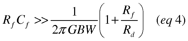
- an amplifier TIA comprises in parallel an operational amplifier AOP or an amplifier with discrete components, a feedback resistance R f and a stability capacitance C f .
- Such a receiver makes it possible to neutralize the influence of the parasitic capacitance C d of the photodiode by means of a virtual mass. It is in first approximation a second order system
- V s being the output voltage of the assembly
- Î D the current generated by the photodiode
- R f the TIA feedback resistance
- ⁇ damping of the receiver
- i + + ⁇ (eq 6)
- i n - and e n being respectively the equivalent noise current at the negative input of the operational amplifier AOP and the equivalent noise voltage at the input of AOP which characterize the amplifier used, k the Boltzmann constant and T the temperature in degrees Kelvin.
- the sensitivity is optimized by choosing the highest possible resistor R f compatible with the pulse processing band.
- the subject of the invention is a receiver of a pulsed light signal which comprises:
- a photodiode capable of generating an electric current l d in response to this light signal, having as characteristic a parasitic capacitance C d ,
- a transimpedance amplifier connected at the input of the photodiode by a connection capacitance C
- It is mainly characterized in that it comprises a series-parallel reactive circuit, constituted by a capacitance C p which, combined with the capacitance C d of the diode, produces a current divider, called an attenuation pad, upstream of the transimpedance amplifier.
- This current divider attenuates the signal without degrading the noise.
- the capacity Cp is typically located in series with the link capacity and integrates it in general.
- the receiver comprises a resistance R d of background current located between the photodiode and the electrical mass, the capacitance C d and said resistor R d having an impedance Z d , and the pad of attenuation is furthermore constituted by a resistor R p in parallel with the capacitance C p , thus forming a parallel electrical network designated aperiodic attenuation pad, of impedance Z p with
- This aperiodic attenuation pad makes it possible to compensate the influence of the resistor Rd and thus to maintain the receiver's response at low frequency.
- the attenuation pad further comprises a switch in parallel with the capacitance C p , so as to obtain a switchable attenuation pad.
- This switch makes it possible to short-circuit or switch the network R p C p .
- the attenuation pad may furthermore comprise a capacitor C op t in parallel with C d , this capacitance C op t possibly being itself switchable.
- the receiver further comprises a reception channel without an attenuation pad comprising another transimpedance amplifier, these reception channels being multiplexed by means of an input switch of these channels and an output switch of these channels synchronized with each other so as to obtain a receiver of different gains.
- these reception channels may be multiplexed with said reception channels, each attenuation pad reception channel having a different attenuation.
- the light signal is typically capable of generating in the photodiode current pulses between 10 nA and 100 mA.
- Figure 1 has already described shows two equivalent schematic representations of a photodiode provided with a stage background resistance
- FIG. 1 b shows schematically a receiver arrangement according to the state of the art comprising a photodiode and an amplifier TIA;
- FIG. 2 diagrammatically represents an example of receiver mounting according to a first embodiment of the invention with a purely capacitive attenuation pad
- FIG. 3a diagrammatically represents an example of receiver mounting according to a second embodiment of the invention, with an aperiodic attenuation pad switched around Rp Cp;
- FIG. 3b diagrammatically represents an example of receiver mounting according to a third embodiment of the invention, with an aperiodic attenuation pad switched around Cd;
- FIG. 3c schematically represents an example of receiver mounting according to a fourth embodiment of the invention, with a compensated aperiodic attenuation pad;
- FIG. 4 diagrammatically shows an example of receiver mounting according to a fifth embodiment of the invention, with several switched reception channels;
- Figure 5a shows the frequency response of a conventional constant bandwidth receiver for three gain values, showing a variation in damping
- Figure 5b shows the frequency response of a constant bandwidth compensated aperiodic pad receiver for three gain values, showing the maintenance of damping.
- the receiver according to the invention is based on the principle of a capacitive current divider bridge instead of being resistive.
- FIG. 2 An example of a capacitive attenuation pad associated with a photodiode 1 equipped with a TIA 2 is shown in FIG. 2. In this figure, particular attention is given to indicating the electric currents.
- the photodiode is an ideal current generator, capacitive due to the parasitic capacitance Cd.
- the signal is attenuated without adding additional noise.
- This attenuation pad 30 constituted by the capacitance Cp is optionally provided with a switch 31 placed in parallel with this capacitor Cp to adapt the gain to the received level.
- the photodiode 1 is generally charged by a resistor Rd so as to absorb the direct current related to the ambient illumination.
- This resistance Rd modifies the impedance of the photodiode which can no longer be considered as purely capacitive.
- the capacitance Cp is then completed with a resistor Rp in parallel, which forms with this capacitance a parallel electrical network designated an aperiodic attenuation pad 30 of impedance Zp proportional to Zd which is the impedance of the circuit of the diode having the resistor R d and the capacitance C d in parallel.
- I F is the current at the output of attenuation pad 30.
- the attenuation of the current becomes independent of the frequency, the additive noise remaining very low since the resistance Rp is large in front of Rd because of the attenuation ratio a.
- This aperiodic attenuation pad 30 is optionally provided with a switch 31 arranged in parallel with Rp and Cp.
- the TIA 2 amplifier no longer sees the same impedance when the attenuation pad is engaged and its transfer function is affected as shown in FIG. 5a for frequency-dependent gain curves for three depreciations ⁇ (of 0.9, 0.7 and 0.5).
- the assembly behaves like a second order system.
- the proper pulsation ⁇ ⁇ corresponds to that of an assembly whose photodiode has a lower parasitic capacitance of a ratio a:
- the static gain Z T is divided by a, which is desired: As soon as an attenuation a is achieved, the receiver's own pulse ⁇ ⁇ increases but the damping ⁇ increases since the damping / pulsation ratio remains constant.
- aperiodic attenuation pad thus modified is then designated "compensated aperiodic attenuation pad”.
- Such a receiver respects the same transfer transfer function engaged or not.
- another switch 44 may be placed in series with the compensation capacitance Ccomp, between it and the ground.
- the compensated aperiodic attenuation pad 30 functions when this other switch 44 is closed and the first one 31 is open and vice versa.
- C p is related to the capacitance Cd of the detector and the attenuation ratio. For a value of Cd between 12 and 18 pF, we thus obtain by the formula
- the proposed solution fig 3b is to increase artificially the capacitance Cd by adding in parallel a capacitance C op t 41, which at equal attenuation makes it possible to increase the value of Cp.
- This capacitance C op t can be switched by a switch 42 placed in series towards ground.
- the attenuation pad assembly 30 and the transimpedance amplifier 2 are designated by reception with attenuation pad 50.
- the attenuation pad can be aperiodic or not, switchable or not, compensated or not, etc.
- a proposed alternative is to use a plurality of receive channels, each of different gain, as in Figure 4 with two gain values.
- the receiver has two reception channels:
- a reception channel 50 with pad optimized with a compensated aperiodic attenuation pad
- a track 50 'of reception without pad comprising only a transimpedance amplifier 2 optimized at maximum gain.
- the channel is typically selected by a switch 61 located at the input of these channels and a switch 62 at the output of these channels, synchronized with each other to obtain a receiver with different gains.
- the input switch 61 is advantageously provided with a link capacity on each of its outputs to a reception channel.
- This receiver is typically integrated with a LIDAR. It can be used as part of a devometer, in particular a semi-differential active that is to say equipped with a designation laser capable of illuminating the target whose backscattering is measured by this receiver.
- the target emits, for example, constant level light pulses, but when the receiver is at a great distance, it can only measure very low level pulses, whereas when it is at short range, it can measure pulses of strong level.
Landscapes
- Engineering & Computer Science (AREA)
- Physics & Mathematics (AREA)
- General Physics & Mathematics (AREA)
- Power Engineering (AREA)
- Electromagnetism (AREA)
- Computer Networks & Wireless Communication (AREA)
- Radar, Positioning & Navigation (AREA)
- Remote Sensing (AREA)
- Spectroscopy & Molecular Physics (AREA)
- Amplifiers (AREA)
Abstract
Description




Claims
Priority Applications (4)
| Application Number | Priority Date | Filing Date | Title |
|---|---|---|---|
| HK16102467.2A HK1214648B (en) | 2012-11-09 | 2013-11-06 | Receiver of a pulsed light signal with wide dynamic range |
| US14/441,822 US9746372B2 (en) | 2012-11-09 | 2013-11-06 | Receiver of a pulsed light signal with wide dynamic range |
| EP13786288.4A EP2917707B1 (fr) | 2012-11-09 | 2013-11-06 | Recepteur d'un signal lumineux impulsionnel a forte dynamique |
| IL238670A IL238670B (en) | 2012-11-09 | 2015-05-07 | Receiver of a pulsed light signal with a wide dynamic range |
Applications Claiming Priority (2)
| Application Number | Priority Date | Filing Date | Title |
|---|---|---|---|
| FR12/03012 | 2012-11-09 | ||
| FR1203012A FR2998051B1 (fr) | 2012-11-09 | 2012-11-09 | Recepteur d'un signal lumineux impulsionnel a forte dynamique |
Publications (1)
| Publication Number | Publication Date |
|---|---|
| WO2014072362A1 true WO2014072362A1 (fr) | 2014-05-15 |
Family
ID=48050794
Family Applications (1)
| Application Number | Title | Priority Date | Filing Date |
|---|---|---|---|
| PCT/EP2013/073198 Ceased WO2014072362A1 (fr) | 2012-11-09 | 2013-11-06 | Recepteur d'un signal lumineux impulsionnel a forte dynamique |
Country Status (5)
| Country | Link |
|---|---|
| US (1) | US9746372B2 (fr) |
| EP (1) | EP2917707B1 (fr) |
| FR (1) | FR2998051B1 (fr) |
| IL (1) | IL238670B (fr) |
| WO (1) | WO2014072362A1 (fr) |
Families Citing this family (5)
| Publication number | Priority date | Publication date | Assignee | Title |
|---|---|---|---|---|
| CN107370461B (zh) * | 2017-07-17 | 2020-07-10 | 电子科技大学 | 一种应用于跨阻放大器的补偿结构 |
| KR102019382B1 (ko) * | 2017-09-29 | 2019-09-06 | 현대오트론 주식회사 | 거리 검출 센서 및 그것의 동작 방법 |
| WO2022090672A1 (fr) * | 2020-10-30 | 2022-05-05 | Oledcomm | Dispositif optoélectronique discret pour un point d'accès ou terminal d'un réseau optique non filaire |
| US11754444B2 (en) * | 2021-03-19 | 2023-09-12 | Rockwell Collins, Inc. | Distributed integrate and dump circuit |
| US12301174B2 (en) * | 2022-03-01 | 2025-05-13 | Bae Systems Information And Electronic Systems Integration Inc. | Transimpedance amplifier having T-network feedback architecture and method thereof |
Citations (4)
| Publication number | Priority date | Publication date | Assignee | Title |
|---|---|---|---|---|
| US4415803A (en) * | 1980-10-22 | 1983-11-15 | Bell Telephone Laboratories, Incorporated | Optical receiver with improved dynamic range |
| US20040036012A1 (en) * | 2002-08-26 | 2004-02-26 | Atsushi Horiguchi | Photodetector |
| US6862322B1 (en) * | 2000-05-19 | 2005-03-01 | International Business Machines Corporation | Switchable-bandwidth optical receiver |
| US20060001493A1 (en) * | 2004-07-02 | 2006-01-05 | Infineon Technologies Fiber Optics Gmbh | Amplifier circuit for converting the current signal from an optical receiving element into a voltage signal |
Family Cites Families (1)
| Publication number | Priority date | Publication date | Assignee | Title |
|---|---|---|---|---|
| US7418213B2 (en) * | 2004-08-12 | 2008-08-26 | Finisar Corporation | Transimpedance amplifier with integrated filtering and reduced parasitic capacitance |
-
2012
- 2012-11-09 FR FR1203012A patent/FR2998051B1/fr active Active
-
2013
- 2013-11-06 US US14/441,822 patent/US9746372B2/en active Active
- 2013-11-06 EP EP13786288.4A patent/EP2917707B1/fr active Active
- 2013-11-06 WO PCT/EP2013/073198 patent/WO2014072362A1/fr not_active Ceased
-
2015
- 2015-05-07 IL IL238670A patent/IL238670B/en active IP Right Grant
Patent Citations (4)
| Publication number | Priority date | Publication date | Assignee | Title |
|---|---|---|---|---|
| US4415803A (en) * | 1980-10-22 | 1983-11-15 | Bell Telephone Laboratories, Incorporated | Optical receiver with improved dynamic range |
| US6862322B1 (en) * | 2000-05-19 | 2005-03-01 | International Business Machines Corporation | Switchable-bandwidth optical receiver |
| US20040036012A1 (en) * | 2002-08-26 | 2004-02-26 | Atsushi Horiguchi | Photodetector |
| US20060001493A1 (en) * | 2004-07-02 | 2006-01-05 | Infineon Technologies Fiber Optics Gmbh | Amplifier circuit for converting the current signal from an optical receiving element into a voltage signal |
Also Published As
| Publication number | Publication date |
|---|---|
| EP2917707A1 (fr) | 2015-09-16 |
| IL238670A0 (en) | 2015-06-30 |
| HK1214648A1 (zh) | 2016-07-29 |
| US20150292942A1 (en) | 2015-10-15 |
| EP2917707B1 (fr) | 2016-09-07 |
| IL238670B (en) | 2019-05-30 |
| FR2998051B1 (fr) | 2014-12-26 |
| US9746372B2 (en) | 2017-08-29 |
| FR2998051A1 (fr) | 2014-05-16 |
Similar Documents
| Publication | Publication Date | Title |
|---|---|---|
| EP2917707B1 (fr) | Recepteur d'un signal lumineux impulsionnel a forte dynamique | |
| JP5165792B2 (ja) | 高利得増幅器と等化回路とを用いた高感度光受信機 | |
| FR2819064A1 (fr) | Regulateur de tension a stabilite amelioree | |
| WO2015110307A1 (fr) | Procede et dispositif de determination de l'impedance d'un element de stockage d'energie d'une batterie | |
| FR2946201A1 (fr) | Annulation d'offset pour amplificateur audio | |
| FR2740924A1 (fr) | Protection d'entree pour un amplificateur a bande passante elevee | |
| FR2482383A1 (fr) | Amplificateur operationnel | |
| WO2014029942A1 (fr) | Dispositif d'amplification analogique destine notamment a un anemometre laser | |
| WO2010072941A2 (fr) | Dispositif pour quantifier et localiser un signal lumineux module a une frequence predeterminee | |
| EP3275083A1 (fr) | Coupleur électrique puissance/données | |
| EP3206038B1 (fr) | Dispositif de mesure d'un courant électrique généré par un amplificateur acoustique pour actionner une enceinte acoustique | |
| FR3018419A1 (fr) | Dispositif et procede de filtrage du pic de resonance dans un circuit d'alimentation d'au moins un haut-parleur en amont de celui-ci | |
| EP0280381B1 (fr) | Circuit de commande de gain d'un amplificateur d'écoute par haut-parleur pour la suppression de l'effet Larsen | |
| WO2011107671A1 (fr) | Convertisseur courant-tension à réflecteur de courant, étage d'entrée d'un amplificateur et amplificateur correspondant | |
| EP1762854A2 (fr) | Dispositif de mesure d'impulsions de courant très brèves | |
| EP3249949B1 (fr) | Dispositif et procede de filtrage du pic de resonance dans un circuit d'alimentation d'au moins un haut-parleur | |
| FR3073283A1 (fr) | Dispositif de protection contre la foudre ameliore pour une entree differentielle | |
| CA2051882A1 (fr) | Dispositif de traitement d'un signal provenant d'un capteur ayant une reponse du type derivatif | |
| FR3054766A1 (fr) | Ensemble a haut-parleur a armature equilibree ameliore | |
| EP4473658B1 (fr) | Amplificateur audio haute performance | |
| EP2568600A1 (fr) | Dispositif de détection doté d'un montage transimpédance | |
| EP0656685B1 (fr) | Dispositif d'amplification à rétroaction | |
| FR2619972A1 (fr) | Etage amplificateur differentiel et configurations de circuits utilisant un tel etage | |
| FR2731078A1 (fr) | Circuit d'adaptation pour un appareil de mesure de champs electriques et appareil de mesure de champs electriques equipe d'un tel circuit | |
| CA2103403A1 (fr) | Capteurs electromagnetiques semi-actifs a fonction de transfert distribuee |
Legal Events
| Date | Code | Title | Description |
|---|---|---|---|
| 121 | Ep: the epo has been informed by wipo that ep was designated in this application |
Ref document number: 13786288 Country of ref document: EP Kind code of ref document: A1 |
|
| REEP | Request for entry into the european phase |
Ref document number: 2013786288 Country of ref document: EP |
|
| WWE | Wipo information: entry into national phase |
Ref document number: 2013786288 Country of ref document: EP |
|
| WWE | Wipo information: entry into national phase |
Ref document number: 238670 Country of ref document: IL |
|
| WWE | Wipo information: entry into national phase |
Ref document number: 14441822 Country of ref document: US |
|
| NENP | Non-entry into the national phase |
Ref country code: DE |