WO2014076966A1 - スパークプラグ - Google Patents
スパークプラグ Download PDFInfo
- Publication number
- WO2014076966A1 WO2014076966A1 PCT/JP2013/006725 JP2013006725W WO2014076966A1 WO 2014076966 A1 WO2014076966 A1 WO 2014076966A1 JP 2013006725 W JP2013006725 W JP 2013006725W WO 2014076966 A1 WO2014076966 A1 WO 2014076966A1
- Authority
- WO
- WIPO (PCT)
- Prior art keywords
- ground electrode
- chip
- tip
- spark plug
- fuel gas
- Prior art date
- Legal status (The legal status is an assumption and is not a legal conclusion. Google has not performed a legal analysis and makes no representation as to the accuracy of the status listed.)
- Ceased
Links
Images









Classifications
-
- H—ELECTRICITY
- H01—ELECTRIC ELEMENTS
- H01T—SPARK GAPS; OVERVOLTAGE ARRESTERS USING SPARK GAPS; SPARKING PLUGS; CORONA DEVICES; GENERATING IONS TO BE INTRODUCED INTO NON-ENCLOSED GASES
- H01T13/00—Sparking plugs
- H01T13/20—Sparking plugs characterised by features of the electrodes or insulation
- H01T13/32—Sparking plugs characterised by features of the electrodes or insulation characterised by features of the earthed electrode
-
- F—MECHANICAL ENGINEERING; LIGHTING; HEATING; WEAPONS; BLASTING
- F02—COMBUSTION ENGINES; HOT-GAS OR COMBUSTION-PRODUCT ENGINE PLANTS
- F02M—SUPPLYING COMBUSTION ENGINES IN GENERAL WITH COMBUSTIBLE MIXTURES OR CONSTITUENTS THEREOF
- F02M57/00—Fuel-injectors combined or associated with other devices
- F02M57/06—Fuel-injectors combined or associated with other devices the devices being sparking plugs
-
- H—ELECTRICITY
- H01—ELECTRIC ELEMENTS
- H01T—SPARK GAPS; OVERVOLTAGE ARRESTERS USING SPARK GAPS; SPARKING PLUGS; CORONA DEVICES; GENERATING IONS TO BE INTRODUCED INTO NON-ENCLOSED GASES
- H01T13/00—Sparking plugs
- H01T13/20—Sparking plugs characterised by features of the electrodes or insulation
- H01T13/39—Selection of materials for electrodes
-
- H—ELECTRICITY
- H01—ELECTRIC ELEMENTS
- H01T—SPARK GAPS; OVERVOLTAGE ARRESTERS USING SPARK GAPS; SPARKING PLUGS; CORONA DEVICES; GENERATING IONS TO BE INTRODUCED INTO NON-ENCLOSED GASES
- H01T13/00—Sparking plugs
- H01T13/40—Sparking plugs structurally combined with other devices
Definitions
- the present invention relates to a spark plug used for an internal combustion engine or the like.
- a spark plug used for an internal combustion engine or the like includes, for example, an insulator having an axial hole extending in the axial direction, a center electrode inserted on the distal end side of the axial hole, and a cylinder provided on the outer periphery of the insulator And a bar-shaped ground electrode fixed to the tip of the metal shell. Further, a gap is formed between the tip of the ground electrode and the tip of the center electrode, and a spark discharge is generated by applying a voltage to the gap.
- the spark discharge generated in the gap may be blown toward the side surface adjacent to the facing surface of the ground electrode due to the influence of the fuel gas flowing in the combustion chamber. If the spark discharge is blown in this way, a spark discharge is formed between the portion of the ground electrode on the side surface where the chip does not exist and the tip of the center electrode, and the side surface of the ground electrode is It will wear out rapidly. As a result, the voltage required for spark discharge (required voltage) is suddenly increased, and it becomes impossible to generate spark discharge at a relatively early time from the start of use (that is, misfire occurs). There is a risk.
- the chip when the chip is bonded to the facing surface of the ground electrode, the fuel gas is likely to directly hit the chip, and the chip is likely to be cooled rapidly. If the chip is cooled rapidly, the difference in thermal stress generated between the chip and the ground electrode becomes large. As a result, there is a possibility that a crack occurs at the joint between the chip and the ground electrode, and the chip is peeled off from the ground electrode.
- the fuel gas flows faster in the combustion chamber in order to improve fuel consumption
- the fuel gas is likely to blow more easily and the tip is likely to be cooled more rapidly. Therefore, the side surface of the ground electrode may be consumed extremely rapidly, or the chip may be easily peeled off from the ground electrode.
- the present invention has been made in view of the above circumstances, and its purpose is to effectively suppress the rapid consumption of the side surface of the ground electrode due to the blowing flow of the spark discharge, and to further remove the chip from the ground electrode.
- An object of the present invention is to provide a spark plug that can be surely prevented.
- the spark plug of this configuration includes a cylindrical insulator having an axial hole penetrating in the axial direction; A center electrode inserted on the tip side of the shaft hole; A cylindrical metal shell provided on the outer periphery of the insulator; A spark plug that is disposed at a tip of the metal shell and includes a ground electrode that forms a gap with the tip of the center electrode; At least a part of itself has a chip joined to a surface disposed at least in the downstream direction of the fuel gas among both side surfaces of the ground electrode, When the size of the gap is G (mm), When the discharge surface of the chip is projected along the axis with respect to a virtual plane including the tip surface of the center electrode, at least a part of the projected area of the discharge surface is the tip of the center electrode in the virtual plane. It is located within the range of 2.5G from the outer periphery of the surface.
- the “gap size G” refers to the shortest distance from the virtual plane including the tip surface of the center electrode to the virtual plane including the surface (facing surface) facing the center electrode of the ground electrode.
- the term “side surface of the ground electrode” refers to a surface other than the tip surface of the ground electrode among the surfaces adjacent to the facing surface of the ground electrode.
- the “discharge surface” refers to a surface located behind the surface of the chip that faces the bonding surface of the ground electrode (the surface of the ground electrode on which the chip is bonded).
- the “surface disposed in the downstream direction of the fuel gas” differs depending on the type of the internal combustion engine (engine), but in general, among the side surfaces of the ground electrode adjacent to the surface facing the center electrode, This is a side surface where wear is advanced with respect to the other side surface when chips are not provided on both side surfaces.
- the chip is bonded to the surface of the ground electrode that is disposed in the downstream direction of the fuel gas. That is, the chip is provided at a position corresponding to the blown spark discharge. Further, when the discharge surface of the chip is projected onto a virtual plane including the front end surface of the center electrode, at least a part of the projected area of the discharge surface is located within a range of 2.5 G from the outer periphery of the front end surface of the center electrode. It is configured. That is, it is configured such that at least a part of the discharge surface is located at a portion where a spark discharge can be formed between the ground electrode and the center electrode.
- the configuration 1 it is possible to prevent the fuel gas from directly hitting the chip, and it is possible to more surely prevent the chip from being rapidly cooled. Therefore, the thermal stress difference generated between the ground electrode and the chip during cooling can be effectively reduced. As a result, the generation of cracks at the joint between the ground electrode and the chip can be effectively suppressed, and the chip can be more reliably prevented from peeling off from the ground electrode.
- the spark plug of this configuration is the above configuration 1, wherein the tip has a thickness of 0.1 mm or more, A portion of 0.1 mm or more from the surface bonded to the ground electrode of the chip is projected from a direction orthogonal to the axis onto a second virtual plane including the side surface of the ground electrode to which the chip is bonded. Then, the area of the projection region of the portion is 0.1 mm 2 or more.
- the “chip thickness” refers to the maximum thickness of the chip based on the surface of the chip bonded to the side surface of the ground electrode.
- the spark plug of the present configuration has the above configuration 1 or 2, when the downstream direction of the fuel gas is defined as the + side and the upstream direction of the fuel gas is defined as the ⁇ side with respect to the front end surface of the center electrode.
- the shortest distance along the direction orthogonal to the axis from the tip surface of the center electrode to the discharge surface of the chip is +1.5 mm or less.
- the distance from the tip surface of the center electrode along the blowing direction of the spark discharge to the discharge surface of the chip is made sufficiently small, and consequently the tip surface of the center electrode along the blowing direction.
- the distance from the ground electrode to the side surface of the ground electrode (the surface to which the chip is bonded) is sufficiently small. Therefore, the growth of the blown-off spark discharge (flame core) can be more reliably prevented from being inhibited by the ground electrode, and the spark discharge (flame core) can be grown larger. As a result, excellent ignitability can be realized.
- a part of the chip includes a facing surface located on the center electrode side of the ground electrode and a back surface located behind the facing surface. It arrange
- the bonding strength of the chip to the ground electrode can be further increased, and the peeling resistance of the chip can be further improved.
- the spark discharge when the spark discharge is blown, the spark discharge can be brought into contact with a portion of the chip that protrudes from the facing surface, and further blowing of the spark discharge can be prevented. Thereby, spark discharge can be maintained over a longer period, and the occurrence of misfire can be effectively suppressed. As a result, the ignitability can be further improved.
- the spark plug of this configuration is characterized in that, in any one of the above configurations 1 to 5, the tip is joined only to a surface disposed in a downstream direction of the fuel gas among both side surfaces of the ground electrode. .
- the spark plug mounting position with respect to the internal combustion engine or the like has shifted from the normal position (for example, the internal combustion engine or the like with the spark plug rotated from the normal position). Even if it is attached to the tip, the tip can be more reliably provided on the surface of the ground electrode that is disposed in the downstream direction of the fuel gas.
- the tip disposed in the upstream direction of the fuel gas may hinder the flow of fuel gas into the gap. Further, the tip disposed in the upstream direction of the fuel gas is likely to be rapidly cooled by the fuel gas and easily peeled off. And there exists a possibility of causing misfire because the chip
- the configuration 6 is configured such that the chip is bonded only to the surface of the ground electrode that is disposed in the downstream direction of the fuel gas. Therefore, the fuel gas can smoothly flow into the gap, and the ignitability can be further improved. In addition, it is possible to more reliably prevent misfires due to chip peeling and to reduce costs.
- the spark plug mounting structure of this configuration is an internal combustion engine to which the spark plug of any of the above configurations 1 to 6 is mounted, and the tip is disposed at least in the downstream direction of the fuel gas on both side surfaces of the ground electrode. It is characterized by being bonded to the surface to be processed.
- the fuel gas can be prevented from directly hitting the tip of the spark plug, and the rapid cooling of the tip can be prevented more reliably. Therefore, the thermal stress difference generated between the ground electrode and the chip during cooling can be effectively reduced. As a result, the generation of cracks at the joint between the ground electrode and the chip can be effectively suppressed, and the chip can be more reliably prevented from peeling off from the ground electrode.
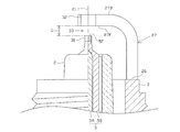
- FIG. 1 is a partially broken front view showing the spark plug 1.
- the direction of the axis CL ⁇ b> 1 of the spark plug 1 is the vertical direction in the drawing, the lower side is the front end side of the spark plug 1, and the upper side is the rear end side.
- the spark plug 1 includes an insulator 2 as a cylindrical insulator, a cylindrical metal shell 3 that holds the insulator 2, and the like.
- the insulator 2 is formed by firing alumina or the like, and in its outer portion, a rear end side body portion 10 formed on the rear end side, and a front end than the rear end side body portion 10.
- a large-diameter portion 11 that protrudes radially outward on the side, a middle body portion 12 that is smaller in diameter than the large-diameter portion 11, and a tip portion that is more distal than the middle body portion 12.
- the leg length part 13 formed in diameter smaller than this on the side is provided.
- the large diameter portion 11, the middle trunk portion 12, and most of the leg length portions 13 are accommodated inside the metal shell 3, while the tip portion of the insulator 2 is The metal shell 3 protrudes further to the front end side than the front end.
- a tapered step portion 14 is formed at the connecting portion between the middle body portion 12 and the long leg portion 13, and the insulator 2 is locked to the metal shell 3 at the step portion 14.
- the insulator 2 is formed with a shaft hole 4 penetrating along the axis CL1, and a center electrode 5 is inserted on the tip side of the shaft hole 4.
- the center electrode 5 includes an inner layer 5A made of a metal having excellent thermal conductivity [for example, copper, copper alloy, pure nickel (Ni)], etc., and an outer layer 5B made of an alloy containing Ni as a main component. . Further, the center electrode 5 has a rod shape (cylindrical shape) as a whole and protrudes from the tip of the insulator 2.
- a predetermined metal for example, iridium (Ir), platinum (Pt), rhodium (Rh), ruthenium (Ru), rhenium (Re), tungsten (W), palladium (Pd ) Or an alloy containing at least one of them as a main component
- a predetermined metal for example, iridium (Ir), platinum (Pt), rhodium (Rh), ruthenium (Ru), rhenium (Re), tungsten (W), palladium (Pd ) Or an alloy containing at least one of them as a main component
- a terminal electrode 6 is inserted and fixed on the rear end side of the shaft hole 4 in a state of protruding from the rear end of the insulator 2.
- a cylindrical resistor 7 is disposed between the center electrode 5 and the terminal electrode 6 of the shaft hole 4. Both ends of the resistor 7 are electrically connected to the center electrode 5 and the terminal electrode 6 through conductive glass seal layers 8 and 9, respectively.
- the metal shell 3 is formed in a cylindrical shape from a metal such as low carbon steel, and a screw portion (male screw portion) 15 for attaching the spark plug 1 to a mounting hole of an internal combustion engine or the like on its outer peripheral surface. Is formed.
- a flange-shaped seat 16 is formed on the rear end side of the screw portion 15, and a ring-shaped gasket 18 is fitted on the screw neck 17 at the rear end of the screw portion 15.
- a tool engaging portion 19 having a hexagonal cross section for engaging a tool such as a wrench when the metal shell 3 is attached to an internal combustion engine or the like is provided.
- 1 is provided with a caulking portion 20 for holding the insulator 2.
- a tapered step portion 21 for locking the insulator 2 is provided on the inner peripheral surface of the metal shell 3.
- the insulator 2 is inserted from the rear end side to the front end side of the metal shell 3, and the step 14 of the metal shell 3 is locked to the step 21 of the metal shell 3. It is fixed by caulking the rear end side opening portion radially inward, that is, by forming the caulking portion 20.
- An annular plate packing 22 is interposed between the step portions 14 and 21. Thereby, the airtightness in the combustion chamber is maintained, and the fuel gas entering the gap between the leg long portion 13 of the insulator 2 exposed to the combustion chamber and the inner peripheral surface of the metal shell 3 is prevented from leaking outside.
- annular ring members 23 and 24 are interposed between the metal shell 3 and the insulator 2 on the rear end side of the metal shell 3, and the ring member 23 , 24 is filled with powder of talc (talc) 25. That is, the metal shell 3 holds the insulator 2 via the plate packing 22, the ring members 23 and 24, and the talc 25.
- the distal end portion 26 of the metal shell 3 is bent back almost in the middle so that the distal end portion is opposed to the distal end portion (center electrode side tip 31) of the center electrode 5.
- a ground electrode 27 is joined.
- the ground electrode 27 is made of an alloy containing Ni as a main component (for example, an alloy containing Ni as a main component and containing at least one of silicon, aluminum, and a rare earth element).
- a gap 33 is formed between the tip of the center electrode 5 (the center electrode side chip 31).
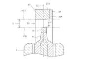
- the size G of the gap 33 is set within a predetermined range (for example, 0.2 mm or more and 2 mm or less). Note that “the size G of the gap 33” is, as shown in FIG.
- the screw portion 15 for the portion of the metal shell 3 to which the ground electrode 27 is fixed is assembled to the internal combustion engine EN by setting the relative formation position of the screw thread to a position corresponding to the starting position of the female thread portion FS formed in the mounting hole HO of the internal combustion engine EN.
- the ground electrode 27 is not disposed between the fuel supply device FJ for supplying the fuel gas to the combustion chamber ER and the gap 33.
- the internal combustion engine EN is configured such that the flow of the fuel gas becomes relatively fast (for example, 10 m / s or more) in the combustion chamber ER in order to improve fuel consumption.
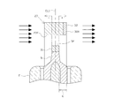
- the ground electrode 27 is disposed at the above-described position, so that the arrow shown by the bold line in FIG. 5 indicates the flow direction of the fuel gas.
- one of the side surfaces 27S1 and 27S2 of the ground electrode 27 is disposed in the upstream direction of the fuel gas, and the other of the side surfaces 27S1 and 27S2 is disposed in the downstream direction of the fuel gas. Therefore, when a voltage is applied to the gap 33 to generate a spark discharge, the spark discharge may be blown by the fuel gas. When the spark discharge is blown, a spark discharge is formed between the side surface of the ground electrode 27 arranged in the downstream direction of the fuel gas and the tip of the center electrode 5 (center electrode tip 31). . As a result, the side surface of the ground electrode 27 disposed in the downstream direction of the fuel gas may be partially consumed due to the spark discharge.
- a rectangular parallelepiped ground electrode side chip 32 is joined.
- the ground electrode side chip 32 is made of a metal having excellent wear resistance (for example, Ir, Pt, Rh, Ru, Re, W, Pd, or an alloy containing at least one of these as a main component). It is joined to the ground electrode 27 while being buried in the ground electrode 27 by resistance welding or the like. In the present embodiment, the ground electrode side chip 32 is joined only to the surface 27S1 arranged in the downstream direction of the fuel gas. Further, the surface of the ground electrode side chip 32 located on the center electrode 5 side is configured to be flush with the opposing surface 27F of the ground electrode 27.
- the shape of the ground electrode side chip 32 is not particularly limited.
- the ground electrode side chip 41 may have a cylindrical shape.
- the first virtual plane VS1 when the discharge surface 32A of the ground electrode side chip 32 is projected along the axis CL1 with respect to the first virtual plane VS1, the first virtual plane VS1
- at least a part of the projection region PR1 of the discharge surface 32A is in a range RA of 2.5 G from the outer periphery of the front end surface 5F of the center electrode 5 (in FIG. 7, a dotted pattern is given). It is comprised so that it may be located in a site
- the “discharge surface 32A” refers to the joint surface of the ground electrode 27 in the ground electrode side chip 32 (the downstream side of the fuel gas among the side surfaces 27S1 and 27S2 of the ground electrode 27). It is a surface arranged in the direction and to which the ground electrode side chip 32 is bonded, and in this embodiment, refers to a surface located behind the surface facing the side surface 27S1).
- the thickness T of the ground electrode side chip 32 (more specifically, the maximum of the ground electrode side chip 32 on the basis of the surface bonded to the side surface 27S1 of the ground electrode side chip 32) Thickness) is 0.1 mm or more.
- a portion 32P of 0.1 mm or more along the thickness direction of the ground electrode side chip 32 from the surface joined to the ground electrode 27 of the ground electrode side chip 32 (a dotted pattern is given in FIG. 8). Portion) is projected from the direction orthogonal to the axis CL1 onto the second virtual plane VS2 including the side surface 27S1 (surface to which the chip 32 is bonded) of the ground electrode 27, the projection region PR2 (in FIG. 8, The area S of the hatched portion) is 0.1 mm 2 or more. That is, the ground electrode side chip 32 is sufficiently thick and has a sufficiently large cross-sectional area at a portion located on the discharge surface 32A side.
- the downstream direction of the fuel gas is defined as the + side with respect to the front end surface 5F of the center electrode 5, and the fuel gas ,
- the shortest distance K along the direction perpendicular to the axis CL1 from the tip surface 5F of the center electrode 5 to the discharge surface 32A is set to +1.5 mm or less. That is, when the spark discharge (flame core) blown by the fuel gas grows, the growth is not suppressed as much as possible by the ground electrode 27.
- the discharge surface 32A When the discharge surface 32A is located on the front end surface 5F of the center electrode 5 (more specifically, the discharge surface 32A extends on the virtual surface obtained by extending the outer periphery of the front end surface 5F along the axis CL1, or The shortest distance K is 0.0 mm).
- the ground electrode side chip 32 is joined to the side surface 27S1 of the ground electrode 27 disposed in the downstream direction of the fuel gas. That is, the ground electrode side chip 32 is provided at a position corresponding to the blown spark discharge. Further, when the discharge surface 32A is projected onto the first virtual plane VS1, at least a part of the projection region PR1 of the discharge surface 32A is located within the range RA of 2.5G from the outer periphery of the front end surface 5F of the center electrode 5. It is configured. In other words, at least a part of the discharge surface 32 ⁇ / b> A is located in a portion of the ground electrode 27 that can form a spark discharge with the center electrode 5.
- a spark discharge can be formed between the ground electrode side tip 32 and the center electrode 5 when a spark discharge is blown by the fuel gas.
- a spark discharge is blown by the fuel gas.
- the present embodiment it is possible to prevent the fuel gas from directly hitting the ground electrode side chip 32, and it is possible to more surely prevent the ground electrode side chip 32 from being rapidly cooled. Therefore, the thermal stress difference generated between the ground electrode 27 and the ground electrode side chip 32 during cooling can be effectively reduced. As a result, the generation of cracks at the joint between the ground electrode 27 and the ground electrode side chip 32 can be effectively suppressed, and the separation of the ground electrode side chip 32 can be more reliably prevented.
- the spark plug 1 when the spark plug 1 is attached to the internal combustion engine EN configured to increase the flow of fuel gas (for example, 10 m / s or more) as in the present embodiment, uneven wear of the ground electrode 27 is caused.
- the above-described configuration can more reliably prevent uneven wear of the ground electrode 27 and peeling of the ground electrode side chip 32.
- joining the ground electrode side tip 31 to at least the side surface disposed in the downstream direction of the fuel gas among the side surfaces 27S1 and 27S2 of the ground electrode 27 increases the flow of the fuel gas (for example, 10 m / s). This is particularly effective in the spark plug used in the internal combustion engine EN configured as described above.
- the thickness T of the ground electrode side chip 32 is set to 0.1 mm or more, and the area S is set to 0.1 mm 2 or more. Therefore, a sufficient consumption volume of the ground electrode side chip 32 can be secured, and the wear resistance can be further improved.
- the shortest distance K is set to +1.5 mm or less, and the distance from the front end surface 5F of the center electrode 5 to the side surface 27S1 of the ground electrode 27 along the blowing direction of the spark discharge is made sufficiently small. Therefore, the growth of the blown-off spark discharge (flame core) can be more reliably prevented from being inhibited by the ground electrode 27, and the spark discharge (flame core) can be grown larger. As a result, excellent ignitability can be realized.
- the ground electrode side tip 32 is joined only to the side surface 27S1 disposed in the downstream direction of the fuel gas in the ground electrode 27, the fuel gas can smoothly flow into the gap 33, and ignition is performed. Further improvement in sex can be achieved.
- a spark plug sample 1 (corresponding to a comparative example) in which the ground electrode side tip is joined to the opposing surface of the ground electrode, and the fuel gas of the ground electrode
- a spark plug sample 2 (corresponding to the example) in which the ground electrode side chip was joined to the side surface arranged in the downstream direction was produced, and a desktop cooling test was performed on both samples.
- the outline of the desk cooling test is as follows. That is, after heating the sample for 2 minutes with a burner so that the ambient temperature of the ground electrode side chip becomes 1000 ° C. in an air atmosphere, the side surface of the ground electrode (sample 2 is the side surface to which the chip is bonded).
- One cycle of blowing air assuming fuel gas to the opposite side surface for 1 minute was performed 1000 cycles. Then, by observing the cross section of the sample after 1000 cycles, the ratio of the length of the oxide scale formed at the boundary portion to the length of the boundary portion between the ground electrode and the ground electrode side chip (oxide scale ratio) is obtained. Measured. Table 1 shows the oxide scale ratio in both samples.
- the outer diameter of the tip surface of the center electrode was 0.8 mm.
- the ground electrode had a thickness of 1.5 mm and a width of 2.8 mm. Further, the ground electrode side tip was formed in a columnar shape, its thickness was 0.3 mm, and its outer diameter was 0.7 mm.
- Sample 2 has a sufficiently small oxide scale ratio and can more reliably prevent the separation of the ground electrode side chip from the ground electrode. This is presumably because rapid cooling of the ground electrode side tip by air (fuel gas) was suppressed, and as a result, the thermal stress difference generated between the ground electrode and the ground electrode side tip was effectively reduced.
- a spark plug sample having a gap size G of 0.8 mm, 1.1 mm, or 1.5 mm is produced, and the center electrode is made negative and the ground electrode is made positive, and spark discharge occurs.
- each sample and the power supply were connected.
- a voltage was applied to the sample in an air atmosphere of 1 MPa while blowing air at a flow rate of 10 m / s or more to the gap (note that the frequency of the applied voltage was set to 100 Hz and 6000 times per minute. A spark discharge was performed).
- size of the said discharge generation distance is corresponded to the magnitude
- FIG. 10 is a graph showing the relationship between the gap size G and the discharge generation distance.
- the outer diameter of the tip surface of the center electrode was set to 0.8 mm.
- the ground electrode had a thickness of 1.5 mm and a width of 2.8 mm. Further, the ground electrode side tip was formed in a columnar shape, its thickness was 0.3 mm, and its outer diameter was 0.7 mm.
- the discharge generation distance is 2.5 times the gap size G. That is, when a virtual surface is formed by extending an annular portion separated by 2.5 G from the outer periphery of the front end surface of the center electrode to the outer peripheral side toward the front end side in the axial direction, the portion of the ground electrode located within the virtual surface is sparked. It was confirmed that it was a part that could be consumed by discharge.
- the ground electrode side chip when providing the ground electrode side chip, it can be said that it is preferable that at least a part of the discharge surface of the ground electrode side chip is located in a portion of the ground electrode located in the virtual plane. .
- the discharge surface of the ground electrode side chip when the discharge surface of the ground electrode side chip is projected along the axis with respect to a virtual plane including the tip surface of the center electrode, at least a part of the projected portion of the discharge surface is the center electrode in the virtual plane. It can be said that it is preferable to be configured so as to be located within a range of 2.5 G from the outer periphery of the tip surface.
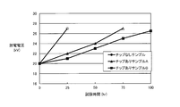
- a sample without a chip and samples A and B with a chip were prepared, and a desktop spark durability test was performed on each sample.
- the outline of the desktop spark durability test is as follows. That is, while connecting each sample and the power supply device so that spark discharge occurs with the center electrode being negative and the ground electrode being positive, while blowing air at a flow rate of 10 m / s or more to the gap, A voltage was applied to the sample over a maximum of 100 hours in an atmospheric atmosphere of 1 MPa (note that the frequency of the applied voltage was 100 Hz and 6000 spark discharges per minute were performed). And the time change of the discharge voltage in each sample was measured for every predetermined time.
- Fig. 11 shows the results of the test.
- the test result of the sample without the chip is indicated by a circle
- the test result of the sample A with the chip is indicated by a triangle
- the test result of the sample B with the chip is indicated by a square mark.
- the occurrence of misfire is indicated by a white mark.
- the tipless sample is a sample of a spark plug configured without providing a ground electrode side tip.
- the ground electrode side tip is provided on the side surface of the ground electrode disposed in the downstream direction of the fuel gas (air in this test), and the thickness T of the ground electrode side tip is 0.1 mm.
- a sample of a spark plug in which the area S is 0.05 mm 2 is provided in the sample B with tip.
- the ground electrode side tip is provided on the side surface of the ground electrode arranged in the downstream direction of the fuel gas (air in this test), and the thickness T of the ground electrode side tip is 0.1 mm.
- a spark plug sample in which the area S is 0.1 mm 2 .
- a sample with a thickness T of 0.1 mm and an area S of 0.1 mm 2 causes misfire even when discharge is caused for 100 hours. It was also found that the discharge voltage rise suppression effect was excellent.
- the thickness T of the ground electrode side tip is set to 0.1 mm or more, and the area S is set to 0. It can be said that the thickness is preferably 1 mm 2 or more.
- the axis from the tip surface of the center electrode to the discharge surface of the tip of the ground electrode side when the downstream direction of the fuel gas is the + side and the upstream direction of the fuel gas is the-side Samples of spark plugs with various changes in the shortest distance K (mm) along the direction perpendicular to the angle were prepared, and an ignition limit evaluation test was performed on each sample.
- the outline of the ignition limit evaluation test is as follows. That is, after each sample was attached to a predetermined engine, the air-fuel ratio (A / F) of the fuel gas was gradually decreased while operating the engine at a rotational speed of 2000 rpm.
- FIG. 12 shows the results of the test. In addition, it can be said that it is excellent in ignitability, so that a limit air fuel ratio is large.
- the shortest distance K along the direction perpendicular to the axis line from the tip surface of the center electrode to the discharge surface of the ground electrode side chip is set to +1.5 mm or less. It can be said that it is preferable.
- the ground electrode side chip 32 is configured such that the surface located on the center electrode 5 side is flush with the opposing surface 27F of the ground electrode 27.
- the relative position of the electrode side tip 32 is not limited to this. Therefore, for example, as shown in FIG. 13, the entire region of the ground electrode side chip 42 may be located on the side farther from the center electrode 5 than the facing surface 27F.
- the surface located on the center electrode 5 side of the ground electrode side chip is made sufficiently close to the opposing surface 27F from the viewpoint of more reliably preventing the ground electrode 27 from being consumed. Is preferred. Therefore, the distance between the surface located on the center electrode 5 side of the ground electrode side chip and the facing surface 27F can be made to be half or less of the thickness of the ground electrode 27 at the portion where the ground electrode side chip is joined. Preferably, it is more preferable to set it to 1/4 or less of the said thickness.
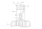
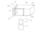
- a part of the ground electrode side chip 43 may protrude from the facing surface 27F toward the center electrode 5 side.
- the ground electrode side chip 32 is joined only to the side surface 27S1 of the ground electrode 27.
- the ground electrode side chips 44, 45 are provided on both side surfaces 27S1, 27S2. You may join.
- the ground electrode side chip 46 is joined to at least the side surface disposed in the downstream direction of the fuel gas among the side surfaces 27S1 and 27S2 of the ground electrode 27, and the tip surface 27A of the ground electrode 27
- a tip surface tip 47 made of a predetermined metal for example, Ir, Pt, Rh, Ru, Re, W, Pd, or an alloy containing at least one of them as a main component
- a predetermined metal for example, Ir, Pt, Rh, Ru, Re, W, Pd, or an alloy containing at least one of them as a main component
- a part of the ground electrode side chip 48 may be arranged on the facing surface 27 ⁇ / b> F located on the center electrode 5 side of the ground electrode 27.
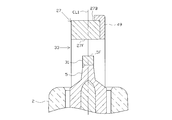
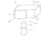
- a part of the ground electrode side chip 49 may be arranged on the back surface 27 ⁇ / b> B located behind the facing surface 27 ⁇ / b> F in the ground electrode 27.
- a part of the ground electrode side chip may be arranged on both the facing surface 27F and the back surface 27B. In this case, the bonding strength of the ground electrode side chip with respect to the ground electrode 27 can be further increased, and peeling of the ground electrode side chip can be more reliably prevented.
- the ground electrode side chip 32 is buried in the ground electrode 27. However, as shown in FIGS. 19 and 20, at least a part of the ground electrode side chips 50 and 51 is formed.
- the ground electrode 27 may protrude from the side surface 27S1.
- the ground electrode 27 is made of a single metal.
- the ground electrode 27 is provided with an inner layer made of copper, a copper alloy or the like having excellent heat conductivity. It is good also as a multilayer structure which consists of an outer layer and an inner layer.
- the tool engaging portion 19 has a hexagonal cross section, but the shape of the tool engaging portion 19 is not limited to such a shape.
- it may be a Bi-HEX (deformed 12-angle) shape [ISO 22777: 2005 (E)].
Landscapes
- Spark Plugs (AREA)
- Ignition Installations For Internal Combustion Engines (AREA)
Abstract
Description
前記軸孔の先端側に挿設された中心電極と、
前記絶縁体の外周に設けられた筒状の主体金具と、
前記主体金具の先端部に配置され、前記中心電極の先端部との間で間隙を形成する接地電極とを備えるスパークプラグであって、
自身の少なくとも一部が、前記接地電極の両側面のうち少なくとも燃料ガスの下流方向に配置される面に接合されるチップを有し、
前記間隙の大きさをG(mm)としたときにおいて、
前記中心電極の先端面を含む仮想平面に対して、前記チップにおける放電面を前記軸線に沿って投影したとき、前記仮想平面において、前記放電面の投影領域の少なくとも一部が前記中心電極の先端面外周から2.5Gの範囲内に位置することを特徴とする。
前記チップのうち前記接地電極に接合されている面から0.1mm以上の部分を前記軸線に直交する方向から前記接地電極のうち前記チップが接合されている前記側面を含む第2仮想平面に投影したとき、前記部分の投影領域の面積が0.1mm2以上であることを特徴とする。
前記中心電極の先端面から前記チップの前記放電面までの前記軸線に直交する方向に沿った最短距離が+1.5mm以下であることを特徴とする。

2…絶縁碍子(絶縁体)
3…主体金具
4…軸孔
5…中心電極
5F…(中心電極の)先端面
27…接地電極
27B…(接地電極の)背面
27F…(接地電極の)対向面
27S1,27S2…(接地電極の)側面
32…接地電極側チップ(チップ)
32A…放電面
33…間隙
VS1…第1仮想平面(仮想平面)
VS2…第2仮想平面
CL1…軸線
PR1…放電面の投影領域
Claims (7)
- 軸線方向に貫通する軸孔を有する筒状の絶縁体と、
前記軸孔の先端側に挿設された中心電極と、
前記絶縁体の外周に設けられた筒状の主体金具と、
前記主体金具の先端部に配置され、前記中心電極の先端部との間で間隙を形成する接地電極とを備えるスパークプラグであって、
自身の少なくとも一部が、前記接地電極の両側面のうち少なくとも燃料ガスの下流方向に配置される面に接合されるチップを有し、
前記間隙の大きさをG(mm)としたときにおいて、
前記中心電極の先端面を含む仮想平面に対して、前記チップにおける放電面を前記軸線に沿って投影したとき、前記仮想平面において、前記放電面の投影領域の少なくとも一部が前記中心電極の先端面外周から2.5Gの範囲内に位置することを特徴とするスパークプラグ。 - 前記チップの厚さが0.1mm以上であり、
前記チップのうち前記接地電極に接合されている面から0.1mm以上の部分を前記軸線に直交する方向から前記接地電極のうち前記チップが接合されている前記側面を含む第2仮想平面に投影したとき、前記部分の投影領域の面積が0.1mm2以上であることを特徴とする請求項1に記載のスパークプラグ。 - 前記中心電極の先端面を基準として、前記燃料ガスの下流方向を+側、前記燃料ガスの上流方向を-側としたとき、
前記中心電極の先端面から前記チップの前記放電面までの前記軸線に直交する方向に沿った最短距離が+1.5mm以下であることを特徴とする請求項1又は2に記載のスパークプラグ。 - 前記チップの一部は、前記接地電極のうち前記中心電極側に位置する対向面、及び、当該対向面の背後に位置する背面のうちの少なくとも一方に配設されることを特徴とする請求項1乃至3のいずれか1項に記載のスパークプラグ。
- 前記チップの一部は、前記接地電極のうち前記中心電極側に位置する対向面よりも前記中心電極側に突出していることを特徴とする請求項1乃至4のいずれか1項に記載のスパークプラグ。
- 前記チップは、前記接地電極の両側面のうち前記燃料ガスの下流方向に配置される面のみに接合されることを特徴とする請求項1乃至5のいずれか1項に記載のスパークプラグ。
- 請求項1~6のいずれか1項に記載のスパークプラグを内燃機関に取り付けてなるスパークプラグの取付構造であって、前記チップは、前記接地電極の両側面のうち少なくとも前記燃料ガスの下流方向に配置される面に接合されていることを特徴とするスパークプラグの取付構造。
Priority Applications (5)
| Application Number | Priority Date | Filing Date | Title |
|---|---|---|---|
| CN201380060309.3A CN104798272B (zh) | 2012-11-19 | 2013-11-15 | 火花塞 |
| EP13855482.9A EP2922157B1 (en) | 2012-11-19 | 2013-11-15 | Spark plug |
| KR1020157012991A KR101738798B1 (ko) | 2012-11-19 | 2013-11-15 | 스파크 플러그 |
| US14/443,764 US9252569B2 (en) | 2012-11-19 | 2013-11-15 | Spark plug |
| JP2014508625A JP5658848B2 (ja) | 2012-11-19 | 2013-11-15 | スパークプラグ |
Applications Claiming Priority (2)
| Application Number | Priority Date | Filing Date | Title |
|---|---|---|---|
| JP2012252980 | 2012-11-19 | ||
| JP2012-252980 | 2012-11-19 |
Publications (1)
| Publication Number | Publication Date |
|---|---|
| WO2014076966A1 true WO2014076966A1 (ja) | 2014-05-22 |
Family
ID=50730897
Family Applications (1)
| Application Number | Title | Priority Date | Filing Date |
|---|---|---|---|
| PCT/JP2013/006725 Ceased WO2014076966A1 (ja) | 2012-11-19 | 2013-11-15 | スパークプラグ |
Country Status (6)
| Country | Link |
|---|---|
| US (1) | US9252569B2 (ja) |
| EP (1) | EP2922157B1 (ja) |
| JP (1) | JP5658848B2 (ja) |
| KR (1) | KR101738798B1 (ja) |
| CN (1) | CN104798272B (ja) |
| WO (1) | WO2014076966A1 (ja) |
Cited By (5)
| Publication number | Priority date | Publication date | Assignee | Title |
|---|---|---|---|---|
| CN110021880A (zh) * | 2018-01-10 | 2019-07-16 | 日本特殊陶业株式会社 | 火花塞 |
| JP2019121590A (ja) * | 2018-01-10 | 2019-07-22 | 日本特殊陶業株式会社 | スパークプラグ |
| JP2021002479A (ja) * | 2019-06-21 | 2021-01-07 | 日本特殊陶業株式会社 | スパークプラグ |
| JP2021002480A (ja) * | 2019-06-21 | 2021-01-07 | 日本特殊陶業株式会社 | スパークプラグ |
| JP2021128869A (ja) * | 2020-02-14 | 2021-09-02 | 日本特殊陶業株式会社 | スパークプラグ |
Families Citing this family (3)
| Publication number | Priority date | Publication date | Assignee | Title |
|---|---|---|---|---|
| DE102017218313B4 (de) * | 2017-10-13 | 2019-08-29 | Ford Global Technologies, Llc | Zündkerze, Brennkammeranordnung und Kraftfahrzeug |
| KR102402639B1 (ko) | 2017-11-24 | 2022-05-26 | 삼성전자주식회사 | 전자 장치 및 그의 통신 방법 |
| CN116852083B (zh) * | 2023-07-03 | 2025-09-23 | 中国北方发动机研究所 | 一种非接触式衔铁气隙调整方法 |
Citations (3)
| Publication number | Priority date | Publication date | Assignee | Title |
|---|---|---|---|---|
| JPS6113588A (ja) * | 1984-06-27 | 1986-01-21 | 日本特殊陶業株式会社 | 点火プラグ用外側電極の製造方法 |
| JP2006236906A (ja) | 2005-02-28 | 2006-09-07 | Ngk Spark Plug Co Ltd | スパークプラグの製造方法 |
| JP2012069376A (ja) | 2010-09-24 | 2012-04-05 | Denso Corp | スパークプラグ及びその製造方法 |
Family Cites Families (13)
| Publication number | Priority date | Publication date | Assignee | Title |
|---|---|---|---|---|
| US4211952A (en) * | 1977-04-07 | 1980-07-08 | Nippon Soken, Inc. | Spark plug |
| JP4543559B2 (ja) * | 2001-02-08 | 2010-09-15 | 株式会社デンソー | スパークプラグ |
| JP4125060B2 (ja) * | 2002-07-16 | 2008-07-23 | 日本特殊陶業株式会社 | スパークプラグ |
| JP4453024B2 (ja) | 2005-08-01 | 2010-04-21 | 株式会社デンソー | 筒内噴射式内燃機関 |
| JP4714046B2 (ja) * | 2006-03-09 | 2011-06-29 | 日本特殊陶業株式会社 | 内燃機関用スパークプラグ |
| US7906894B2 (en) * | 2007-12-19 | 2011-03-15 | Ngk Spark Plug Co., Ltd. | Spark plug for internal combustion engine |
| WO2009087894A1 (ja) * | 2008-01-10 | 2009-07-16 | Ngk Spark Plug Co., Ltd. | 内燃機関用スパークプラグ及びその製造方法 |
| JP5476123B2 (ja) * | 2008-04-09 | 2014-04-23 | 日本特殊陶業株式会社 | 内燃機関用スパークプラグ |
| WO2010038611A1 (ja) * | 2008-09-30 | 2010-04-08 | 日本特殊陶業株式会社 | 内燃機関用スパークプラグ |
| JP4996723B2 (ja) * | 2010-07-02 | 2012-08-08 | 日本特殊陶業株式会社 | スパークプラグ及びその製造方法 |
| JP5238096B2 (ja) * | 2010-12-20 | 2013-07-17 | 日本特殊陶業株式会社 | スパークプラグ及びその製造方法 |
| JP5530942B2 (ja) * | 2011-01-19 | 2014-06-25 | 日本特殊陶業株式会社 | スパークプラグの取付構造およびスパークプラグ |
| US8823251B2 (en) * | 2012-07-06 | 2014-09-02 | Denso International America, Inc. | Partial shroud of spark plug for ground electrode heat dispersion |
-
2013
- 2013-11-15 JP JP2014508625A patent/JP5658848B2/ja active Active
- 2013-11-15 CN CN201380060309.3A patent/CN104798272B/zh active Active
- 2013-11-15 WO PCT/JP2013/006725 patent/WO2014076966A1/ja not_active Ceased
- 2013-11-15 KR KR1020157012991A patent/KR101738798B1/ko not_active Expired - Fee Related
- 2013-11-15 EP EP13855482.9A patent/EP2922157B1/en active Active
- 2013-11-15 US US14/443,764 patent/US9252569B2/en active Active
Patent Citations (3)
| Publication number | Priority date | Publication date | Assignee | Title |
|---|---|---|---|---|
| JPS6113588A (ja) * | 1984-06-27 | 1986-01-21 | 日本特殊陶業株式会社 | 点火プラグ用外側電極の製造方法 |
| JP2006236906A (ja) | 2005-02-28 | 2006-09-07 | Ngk Spark Plug Co Ltd | スパークプラグの製造方法 |
| JP2012069376A (ja) | 2010-09-24 | 2012-04-05 | Denso Corp | スパークプラグ及びその製造方法 |
Cited By (9)
| Publication number | Priority date | Publication date | Assignee | Title |
|---|---|---|---|---|
| CN110021880A (zh) * | 2018-01-10 | 2019-07-16 | 日本特殊陶业株式会社 | 火花塞 |
| JP2019121590A (ja) * | 2018-01-10 | 2019-07-22 | 日本特殊陶業株式会社 | スパークプラグ |
| CN110021880B (zh) * | 2018-01-10 | 2020-07-14 | 日本特殊陶业株式会社 | 火花塞 |
| JP2021002479A (ja) * | 2019-06-21 | 2021-01-07 | 日本特殊陶業株式会社 | スパークプラグ |
| JP2021002480A (ja) * | 2019-06-21 | 2021-01-07 | 日本特殊陶業株式会社 | スパークプラグ |
| JP7060550B2 (ja) | 2019-06-21 | 2022-04-26 | 日本特殊陶業株式会社 | スパークプラグ |
| JP7060551B2 (ja) | 2019-06-21 | 2022-04-26 | 日本特殊陶業株式会社 | スパークプラグ |
| JP2021128869A (ja) * | 2020-02-14 | 2021-09-02 | 日本特殊陶業株式会社 | スパークプラグ |
| JP7227933B2 (ja) | 2020-02-14 | 2023-02-22 | 日本特殊陶業株式会社 | スパークプラグ |
Also Published As
| Publication number | Publication date |
|---|---|
| JP5658848B2 (ja) | 2015-01-28 |
| KR101738798B1 (ko) | 2017-05-22 |
| KR20150074091A (ko) | 2015-07-01 |
| CN104798272A (zh) | 2015-07-22 |
| EP2922157A1 (en) | 2015-09-23 |
| US9252569B2 (en) | 2016-02-02 |
| EP2922157A4 (en) | 2016-07-13 |
| JPWO2014076966A1 (ja) | 2017-01-05 |
| EP2922157B1 (en) | 2017-10-18 |
| US20150288149A1 (en) | 2015-10-08 |
| CN104798272B (zh) | 2016-12-21 |
Similar Documents
| Publication | Publication Date | Title |
|---|---|---|
| JP5658848B2 (ja) | スパークプラグ | |
| JP5476123B2 (ja) | 内燃機関用スパークプラグ | |
| JP5271420B2 (ja) | スパークプラグ | |
| JP5525575B2 (ja) | スパークプラグ | |
| CN104782006A (zh) | 火花塞 | |
| CN101682174A (zh) | 火花塞 | |
| KR101348019B1 (ko) | 플라즈마 젯 점화 플러그 | |
| JP5622991B2 (ja) | スパークプラグ | |
| JP5227466B2 (ja) | プラズマジェット点火プラグ | |
| CN103959581B (zh) | 火花塞 | |
| JP5809664B2 (ja) | スパークプラグ | |
| JP5167334B2 (ja) | スパークプラグ | |
| JP5606404B2 (ja) | スパークプラグ | |
| JP2019139946A (ja) | スパークプラグ | |
| JP5698686B2 (ja) | スパークプラグ | |
| JP4699918B2 (ja) | スパークプラグ | |
| JP2013254670A (ja) | スパークプラグ | |
| JP2006202684A (ja) | スパークプラグ | |
| JP6875301B2 (ja) | スパークプラグ | |
| JP2019102409A (ja) | スパークプラグ |
Legal Events
| Date | Code | Title | Description |
|---|---|---|---|
| ENP | Entry into the national phase |
Ref document number: 2014508625 Country of ref document: JP Kind code of ref document: A |
|
| 121 | Ep: the epo has been informed by wipo that ep was designated in this application |
Ref document number: 13855482 Country of ref document: EP Kind code of ref document: A1 |
|
| ENP | Entry into the national phase |
Ref document number: 20157012991 Country of ref document: KR Kind code of ref document: A |
|
| REEP | Request for entry into the european phase |
Ref document number: 2013855482 Country of ref document: EP |
|
| WWE | Wipo information: entry into national phase |
Ref document number: 2013855482 Country of ref document: EP |
|
| NENP | Non-entry into the national phase |
Ref country code: DE |
|
| WWE | Wipo information: entry into national phase |
Ref document number: 14443764 Country of ref document: US |