WO2014092066A1 - 光電変換素子 - Google Patents
光電変換素子 Download PDFInfo
- Publication number
- WO2014092066A1 WO2014092066A1 PCT/JP2013/083045 JP2013083045W WO2014092066A1 WO 2014092066 A1 WO2014092066 A1 WO 2014092066A1 JP 2013083045 W JP2013083045 W JP 2013083045W WO 2014092066 A1 WO2014092066 A1 WO 2014092066A1
- Authority
- WO
- WIPO (PCT)
- Prior art keywords
- photoelectric conversion
- dye
- group
- layer
- pyrazole
- Prior art date
- Legal status (The legal status is an assumption and is not a legal conclusion. Google has not performed a legal analysis and makes no representation as to the accuracy of the status listed.)
- Ceased
Links
- 0 *c1cc(-c2cc(*)cc(-c3*4ccc(*)c3)*2-*2c3cccc2CO*42OC3)*2cc1 Chemical compound *c1cc(-c2cc(*)cc(-c3*4ccc(*)c3)*2-*2c3cccc2CO*42OC3)*2cc1 0.000 description 2
Images


Classifications
-
- C—CHEMISTRY; METALLURGY
- C07—ORGANIC CHEMISTRY
- C07D—HETEROCYCLIC COMPOUNDS
- C07D213/00—Heterocyclic compounds containing six-membered rings, not condensed with other rings, with one nitrogen atom as the only ring hetero atom and three or more double bonds between ring members or between ring members and non-ring members
- C07D213/02—Heterocyclic compounds containing six-membered rings, not condensed with other rings, with one nitrogen atom as the only ring hetero atom and three or more double bonds between ring members or between ring members and non-ring members having three double bonds between ring members or between ring members and non-ring members
- C07D213/04—Heterocyclic compounds containing six-membered rings, not condensed with other rings, with one nitrogen atom as the only ring hetero atom and three or more double bonds between ring members or between ring members and non-ring members having three double bonds between ring members or between ring members and non-ring members having no bond between the ring nitrogen atom and a non-ring member or having only hydrogen or carbon atoms directly attached to the ring nitrogen atom
- C07D213/60—Heterocyclic compounds containing six-membered rings, not condensed with other rings, with one nitrogen atom as the only ring hetero atom and three or more double bonds between ring members or between ring members and non-ring members having three double bonds between ring members or between ring members and non-ring members having no bond between the ring nitrogen atom and a non-ring member or having only hydrogen or carbon atoms directly attached to the ring nitrogen atom with hetero atoms or with carbon atoms having three bonds to hetero atoms with at the most one bond to halogen, e.g. ester or nitrile radicals, directly attached to ring carbon atoms
- C07D213/78—Carbon atoms having three bonds to hetero atoms, with at the most one bond to halogen, e.g. ester or nitrile radicals
- C07D213/79—Acids; Esters
-
- H—ELECTRICITY
- H01—ELECTRIC ELEMENTS
- H01G—CAPACITORS; CAPACITORS, RECTIFIERS, DETECTORS, SWITCHING DEVICES, LIGHT-SENSITIVE OR TEMPERATURE-SENSITIVE DEVICES OF THE ELECTROLYTIC TYPE
- H01G9/00—Electrolytic capacitors, rectifiers, detectors, switching devices, light-sensitive or temperature-sensitive devices; Processes of their manufacture
- H01G9/20—Light-sensitive devices
- H01G9/2059—Light-sensitive devices comprising an organic dye as the active light absorbing material, e.g. adsorbed on an electrode or dissolved in solution
- H01G9/2063—Light-sensitive devices comprising an organic dye as the active light absorbing material, e.g. adsorbed on an electrode or dissolved in solution comprising a mixture of two or more dyes
-
- C—CHEMISTRY; METALLURGY
- C07—ORGANIC CHEMISTRY
- C07D—HETEROCYCLIC COMPOUNDS
- C07D409/00—Heterocyclic compounds containing two or more hetero rings, at least one ring having sulfur atoms as the only ring hetero atoms
- C07D409/14—Heterocyclic compounds containing two or more hetero rings, at least one ring having sulfur atoms as the only ring hetero atoms containing three or more hetero rings
-
- C—CHEMISTRY; METALLURGY
- C07—ORGANIC CHEMISTRY
- C07F—ACYCLIC, CARBOCYCLIC OR HETEROCYCLIC COMPOUNDS CONTAINING ELEMENTS OTHER THAN CARBON, HYDROGEN, HALOGEN, OXYGEN, NITROGEN, SULFUR, SELENIUM OR TELLURIUM
- C07F15/00—Compounds containing elements of Groups 8, 9, 10 or 18 of the Periodic Table
- C07F15/0006—Compounds containing elements of Groups 8, 9, 10 or 18 of the Periodic Table compounds of the platinum group
- C07F15/0046—Ruthenium compounds
- C07F15/0053—Ruthenium compounds without a metal-carbon linkage
-
- C—CHEMISTRY; METALLURGY
- C09—DYES; PAINTS; POLISHES; NATURAL RESINS; ADHESIVES; COMPOSITIONS NOT OTHERWISE PROVIDED FOR; APPLICATIONS OF MATERIALS NOT OTHERWISE PROVIDED FOR
- C09B—ORGANIC DYES OR CLOSELY-RELATED COMPOUNDS FOR PRODUCING DYES, e.g. PIGMENTS; MORDANTS; LAKES
- C09B23/00—Methine or polymethine dyes, e.g. cyanine dyes
- C09B23/10—The polymethine chain containing an even number of >CH- groups
- C09B23/105—The polymethine chain containing an even number of >CH- groups two >CH- groups
-
- C—CHEMISTRY; METALLURGY
- C09—DYES; PAINTS; POLISHES; NATURAL RESINS; ADHESIVES; COMPOSITIONS NOT OTHERWISE PROVIDED FOR; APPLICATIONS OF MATERIALS NOT OTHERWISE PROVIDED FOR
- C09B—ORGANIC DYES OR CLOSELY-RELATED COMPOUNDS FOR PRODUCING DYES, e.g. PIGMENTS; MORDANTS; LAKES
- C09B49/00—Sulfur dyes
-
- C—CHEMISTRY; METALLURGY
- C09—DYES; PAINTS; POLISHES; NATURAL RESINS; ADHESIVES; COMPOSITIONS NOT OTHERWISE PROVIDED FOR; APPLICATIONS OF MATERIALS NOT OTHERWISE PROVIDED FOR
- C09B—ORGANIC DYES OR CLOSELY-RELATED COMPOUNDS FOR PRODUCING DYES, e.g. PIGMENTS; MORDANTS; LAKES
- C09B57/00—Other synthetic dyes of known constitution
- C09B57/10—Metal complexes of organic compounds not being dyes in uncomplexed form
-
- H—ELECTRICITY
- H01—ELECTRIC ELEMENTS
- H01G—CAPACITORS; CAPACITORS, RECTIFIERS, DETECTORS, SWITCHING DEVICES, LIGHT-SENSITIVE OR TEMPERATURE-SENSITIVE DEVICES OF THE ELECTROLYTIC TYPE
- H01G9/00—Electrolytic capacitors, rectifiers, detectors, switching devices, light-sensitive or temperature-sensitive devices; Processes of their manufacture
- H01G9/20—Light-sensitive devices
- H01G9/2004—Light-sensitive devices characterised by the electrolyte, e.g. comprising an organic electrolyte
- H01G9/2013—Light-sensitive devices characterised by the electrolyte, e.g. comprising an organic electrolyte the electrolyte comprising ionic liquids, e.g. alkyl imidazolium iodide
-
- H—ELECTRICITY
- H01—ELECTRIC ELEMENTS
- H01G—CAPACITORS; CAPACITORS, RECTIFIERS, DETECTORS, SWITCHING DEVICES, LIGHT-SENSITIVE OR TEMPERATURE-SENSITIVE DEVICES OF THE ELECTROLYTIC TYPE
- H01G9/00—Electrolytic capacitors, rectifiers, detectors, switching devices, light-sensitive or temperature-sensitive devices; Processes of their manufacture
- H01G9/20—Light-sensitive devices
- H01G9/2059—Light-sensitive devices comprising an organic dye as the active light absorbing material, e.g. adsorbed on an electrode or dissolved in solution
-
- H—ELECTRICITY
- H01—ELECTRIC ELEMENTS
- H01M—PROCESSES OR MEANS, e.g. BATTERIES, FOR THE DIRECT CONVERSION OF CHEMICAL ENERGY INTO ELECTRICAL ENERGY
- H01M14/00—Electrochemical current or voltage generators not provided for in groups H01M6/00 - H01M12/00; Manufacture thereof
-
- H—ELECTRICITY
- H10—SEMICONDUCTOR DEVICES; ELECTRIC SOLID-STATE DEVICES NOT OTHERWISE PROVIDED FOR
- H10K—ORGANIC ELECTRIC SOLID-STATE DEVICES
- H10K85/00—Organic materials used in the body or electrodes of devices covered by this subclass
- H10K85/30—Coordination compounds
- H10K85/341—Transition metal complexes, e.g. Ru(II)polypyridine complexes
- H10K85/344—Transition metal complexes, e.g. Ru(II)polypyridine complexes comprising ruthenium
-
- H—ELECTRICITY
- H10—SEMICONDUCTOR DEVICES; ELECTRIC SOLID-STATE DEVICES NOT OTHERWISE PROVIDED FOR
- H10K—ORGANIC ELECTRIC SOLID-STATE DEVICES
- H10K85/00—Organic materials used in the body or electrodes of devices covered by this subclass
- H10K85/60—Organic compounds having low molecular weight
- H10K85/649—Aromatic compounds comprising a hetero atom
- H10K85/657—Polycyclic condensed heteroaromatic hydrocarbons
- H10K85/6572—Polycyclic condensed heteroaromatic hydrocarbons comprising only nitrogen in the heteroaromatic polycondensed ring system, e.g. phenanthroline or carbazole
-
- H—ELECTRICITY
- H01—ELECTRIC ELEMENTS
- H01G—CAPACITORS; CAPACITORS, RECTIFIERS, DETECTORS, SWITCHING DEVICES, LIGHT-SENSITIVE OR TEMPERATURE-SENSITIVE DEVICES OF THE ELECTROLYTIC TYPE
- H01G9/00—Electrolytic capacitors, rectifiers, detectors, switching devices, light-sensitive or temperature-sensitive devices; Processes of their manufacture
- H01G9/20—Light-sensitive devices
- H01G9/2004—Light-sensitive devices characterised by the electrolyte, e.g. comprising an organic electrolyte
-
- H—ELECTRICITY
- H01—ELECTRIC ELEMENTS
- H01G—CAPACITORS; CAPACITORS, RECTIFIERS, DETECTORS, SWITCHING DEVICES, LIGHT-SENSITIVE OR TEMPERATURE-SENSITIVE DEVICES OF THE ELECTROLYTIC TYPE
- H01G9/00—Electrolytic capacitors, rectifiers, detectors, switching devices, light-sensitive or temperature-sensitive devices; Processes of their manufacture
- H01G9/20—Light-sensitive devices
- H01G9/2027—Light-sensitive devices comprising an oxide semiconductor electrode
- H01G9/2031—Light-sensitive devices comprising an oxide semiconductor electrode comprising titanium oxide, e.g. TiO2
-
- Y—GENERAL TAGGING OF NEW TECHNOLOGICAL DEVELOPMENTS; GENERAL TAGGING OF CROSS-SECTIONAL TECHNOLOGIES SPANNING OVER SEVERAL SECTIONS OF THE IPC; TECHNICAL SUBJECTS COVERED BY FORMER USPC CROSS-REFERENCE ART COLLECTIONS [XRACs] AND DIGESTS
- Y02—TECHNOLOGIES OR APPLICATIONS FOR MITIGATION OR ADAPTATION AGAINST CLIMATE CHANGE
- Y02E—REDUCTION OF GREENHOUSE GAS [GHG] EMISSIONS, RELATED TO ENERGY GENERATION, TRANSMISSION OR DISTRIBUTION
- Y02E10/00—Energy generation through renewable energy sources
- Y02E10/50—Photovoltaic [PV] energy
- Y02E10/542—Dye sensitized solar cells
Definitions
- the present invention relates to a photoelectric conversion element.
- Patent Document 1 Japanese Patent Laid-Open No. 1-220380
- a photoelectric conversion material and an electrolyte material having an absorption spectrum in the visible light region by adsorbing a photosensitizing dye between two electrodes formed on the surface of a glass substrate A photoelectric conversion layer made of is sandwiched (such a solar cell may be referred to as a “dye-sensitized solar cell”).
- Patent Document 2 Japanese Patent Application Laid-Open No. 2003-331936
- Patent Document 3 Japanese Patent Application Laid-Open No. 2004-47229
- Patent Document 4 Japanese Patent Application Laid-Open No. 2005-216490
- 2-n-propylpyridine, an aminopyridine-based compound and a pyrazole-based compound are added to an electrolyte solution mainly for the purpose of improving the above.
- Patent Document 5 Japanese Patent Application Laid-Open No.
- 2006-134615 discloses a 5-membered or 6-membered ring containing two or more nitrogen atoms and having no substituent for the main purpose of improving the open circuit voltage of a solar cell.
- a solar cell containing a nitrogen-containing heterocyclic compound comprising an aromatic ring is described.
- the molecular weight of the additive to the electrolyte solution may be increased.
- the viscosity of the electrolyte solution is increased, and further, the photoelectric conversion efficiency of the solar cell is decreased.
- Patent Document 5 by using a cyclic base having a small molecular size but a high boiling point, volatilization of the base is suppressed, and the photoelectric conversion efficiency of the solar cell is improved and its durability is also improved.
- This invention is made
- the place made into the objective is to provide the photoelectric conversion element by which the performance fall by the heat
- a conductive layer, a photoelectric conversion layer, and a counter electrode are provided, and at least the photoelectric conversion layer is filled with an electrolyte.
- an electrolyte In the photoelectric conversion layer, at least one of a dye made of a compound having one thiocyanate group and a dye made of a compound not having a thiocyanate group is adsorbed to the porous semiconductor layer made of a semiconductor material.
- the electrolyte includes at least one of pyrazole and a pyrazole derivative.
- the dye may be a first metal complex having a terpyridyl group and having no more than one thiocyanate group.
- the dye may be a second metal complex having two or more bipyridyl groups and no thiocyanate group.
- the pyrazole derivative may be one in which one or two of the hydrogen atoms constituting the pyrazole are substituted by an atom or atomic group other than a hydrogen atom, and the hydrogen atom constituting the pyrazole is a methyl group or an ethyl group. , Substituted with at least one of a propyl group and a butyl group.
- FIG. 1 is a cross-sectional view illustrating an example of a configuration of a photoelectric conversion element according to the present invention.
- the conductive layer 2, the photoelectric conversion layer 3, and the counter electrode 8 are sequentially provided on the support substrate 1, and an electrolyte is filled between the photoelectric conversion layer 3 and the counter electrode 8.
- the charge transport layer 4 is formed.
- the photoelectric conversion layer 3 and the charge transport layer 4 are preferably sealed with a sealing portion 9.
- At least one of a dye made of a compound having one thiocyanate group and a dye made of a compound not having a thiocyanate group is adsorbed to the porous semiconductor layer made of a semiconductor material.
- the electrolyte includes at least one of pyrazole and a pyrazole derivative.
- the thiocyanate group is negatively charged. Therefore, a repulsive force based on electrostatic interaction is generated between the unshared electron pair of the nitrogen atom in the pyrazole or the pyrazole derivative and the thiocyanate group.
- the dye has two or more thiocyanate groups, the interaction between the lone pair of nitrogen atom in the pyrazole or pyrazole derivative and the dye may be weakened by the repulsive force. May be invited.
- the photoelectric conversion efficiency of the photoelectric conversion element is increased. However, its heat resistance is significantly reduced.
- at least one of a dye comprising a compound having one thiocyanate group and a dye comprising a compound not having a thiocyanate group is used, and at least one of pyrazole and a pyrazole derivative is an electrolyte. Therefore, the heat resistance is remarkably improved.
- the material which comprises the support substrate 1 will not be specifically limited if it is a material which can generally be used for the support substrate of a photoelectric conversion element, and can exhibit the effect of this invention. However, since light transmissivity is required in the portion that becomes the light receiving surface of the photoelectric conversion element, the support substrate 1 is preferably made of a material having light transmissivity.
- the support substrate 1 may be, for example, a glass substrate made of soda glass, fused silica glass, crystal quartz glass, or the like, or may be a flexible film made of a heat resistant resin material.
- the support substrate 1 when used as a light receiving surface, it substantially transmits at least light having a wavelength having effective sensitivity to a dye described later (the transmittance of the light is, for example, 80% or more). (Preferably 90% or more), and need not necessarily be transparent to light in all wavelength regions.
- film examples include tetraacetyl cellulose (TAC), polyethylene terephthalate (PET), polyphenylene sulfide (PPS), polycarbonate (PC), and polyarylate (PA). ), Polyetherimide (PEI), phenoxy resin or polytetrafluoroethylene.
- TAC tetraacetyl cellulose
- PET polyethylene terephthalate
- PPS polyphenylene sulfide
- PC polycarbonate
- PA polyarylate
- PEI Polyetherimide
- phenoxy resin examples include polytetrafluoroethylene.
- the support substrate 1 can be used when the completed photoelectric conversion element 10 is attached to another structure. That is, it is possible to easily attach the peripheral portion of the support substrate 1 made of a glass substrate or the like to another support using metal processed parts and screws.
- the thickness of the support substrate 1 is not particularly limited, but is preferably about 0.2 to 5 mm in consideration of light transmittance and the like.
- the material which comprises the conductive layer 2 will not be specifically limited if it is a material which can generally be used for the conductive layer of a photoelectric conversion element, and can exhibit the effect of this invention. However, since the conductive layer 2 serves as a light receiving surface of the photoelectric conversion element 10, it requires light transmission, and therefore is preferably made of a material having light transmission.
- the conductive layer 2 is preferably made of, for example, indium tin composite oxide (ITO), tin oxide doped with fluorine (FTO), zinc oxide (ZnO), or the like.
- the conductive layer 2 substantially transmits light having a wavelength having an effective sensitivity to at least a dye described later (the transmittance of the light is, for example, 80% or more, preferably 90% or more). ), And need not be transparent to light in all wavelength regions.
- the thickness of the conductive layer 2 is not particularly limited, but is preferably about 0.02 to 5 ⁇ m.
- the film resistance of the conductive layer 2 is preferably as low as possible, and is preferably 40 ⁇ / sq or less.
- the conductive layer 2 may be provided with a metal lead wire to reduce resistance.
- the metal lead wire material include platinum, gold, silver, copper, aluminum, nickel, and titanium.
- the thickness of the metal lead wire is not particularly limited, but if the metal lead wire is too thick, the amount of incident light from the light receiving surface may be reduced. Therefore, the thickness of the metal lead wire is preferably about 0.1 to 4 mm.
- a structure in which the conductive layer 2 is formed on the surface of the support substrate 1 may be referred to as a “transparent electrode substrate 11”.
- a transparent electrode substrate 11 examples include a transparent electrode substrate in which a conductive layer 2 made of FTO is formed on a support substrate 1 made of soda-lime float glass. This transparent electrode substrate is suitably used in the present invention.
- the photoelectric conversion layer 3 has a porous semiconductor layer made of a semiconductor material. At least one of a dye made of a compound having one thiocyanate group and a dye made of a compound not having a thiocyanate group is adsorbed to the porous semiconductor layer, and preferably filled with an electrolyte.
- porous semiconductor layer examples include a bulk made of a semiconductor material, a layer containing a particulate semiconductor material, or a film made of a semiconductor material in which a large number of micropores are formed.
- the film is preferably made of a semiconductor material having holes formed therein.
- the porosity of the porous semiconductor layer means that the porosity is 20% or more, and the specific surface area is 0.5 to 300 m 2 / g. If the specific surface area of the porous semiconductor layer is 0.5 to 300 m 2 / g, many dyes can be adsorbed, and sunlight can be absorbed efficiently. From the viewpoint of sufficiently securing the amount of dye adsorbed, the specific surface area of the porous semiconductor layer is more preferably about 10 to 200 m 2 / g. Moreover, if the porosity of the porous semiconductor layer is 20% or more, the electrolyte can be sufficiently diffused, and thus electrons can be smoothly returned to the photoelectric conversion layer 3.
- the porosity of the porous semiconductor layer is obtained by calculation from the thickness of the porous semiconductor layer, the mass of the porous semiconductor layer, and the density of the semiconductor material.
- the specific surface area of the porous semiconductor layer is determined by the BET method which is a gas adsorption method.
- the semiconductor material constituting the porous semiconductor layer (hereinafter simply referred to as “semiconductor material”) is not particularly limited as long as it is generally used for a photoelectric conversion material.
- the semiconductor material may be a metal oxide such as titanium oxide, zinc oxide, tin oxide, iron oxide, niobium oxide, cerium oxide, tungsten oxide, nickel oxide or strontium titanate, cadmium sulfide, lead sulfide, etc.
- Zinc sulfide, indium phosphide, copper-indium sulfide (CuInS 2 ), CuAlO 2, or SrCu 2 O 2 may be used.
- one of the listed materials may be used alone, or two or more of the listed materials may be used in combination. From the viewpoint of photoelectric conversion efficiency, stability and safety, it is preferable to use titanium oxide as a material constituting the porous semiconductor layer.
- the titanium oxide to be used is variously narrowly defined such as anatase type titanium oxide, rutile type titanium oxide, amorphous titanium oxide, metatitanic acid or orthotitanic acid. It may be titanium oxide, titanium hydroxide, or hydrous titanium oxide. These titanium oxides may be used alone or in combination. Anatase-type titanium oxide and rutile-type titanium oxide can be in either form depending on the production method or thermal history, but anatase-type titanium oxide is common.
- the average particle size of the semiconductor material is not particularly limited. However, since the light scattering property of the photoelectric conversion layer 3 can be adjusted by changing the average particle size of the semiconductor material, it is preferable to appropriately set the average particle size of the semiconductor material in consideration of this. Specifically, the light scattering property is improved when the average particle size of the semiconductor material is increased, although it cannot be generally described because of the formation conditions of the photoelectric conversion layer 3 and the like. Therefore, when the porous semiconductor layer includes a semiconductor material having a large average particle diameter, the photoelectric conversion layer 3 including the porous semiconductor layer is excellent in light scattering properties, which contributes to an improvement in the light capture rate. On the other hand, when the average particle size of the semiconductor material becomes small, the adsorption point of the dye increases.
- the porous semiconductor layer may be a single layer made of a semiconductor material having substantially the same average particle diameter, but a layer made of a semiconductor material having a relatively small average particle diameter and a semiconductor material having a relatively large average particle diameter
- a layer made of The semiconductor material having a relatively small average particle diameter preferably has an average particle diameter of 5 nm or more and less than 50 nm, and more preferably has an average particle diameter of 10 nm or more and 30 nm or less.
- the semiconductor material having a relatively large average particle size preferably has an average particle size of 50 nm or more, more preferably 50 nm or more and 600 nm or less, and more preferably 50 nm or more and 100 nm or less. More preferably, it has an average particle size. In terms of effective use of incident light for photoelectric conversion, it is preferable that the average particle size of the semiconductor material is uniform to some extent as in a commercially available semiconductor material.
- the semiconductor material is preferably titanium oxide having an average particle size of 50 nm or more, and more preferably titanium oxide having an average particle size of 50 nm to 100 nm. .
- the average particle diameter is a value obtained using a diffraction peak obtained by XRD (X-ray diffraction).
- the average particle diameter can be obtained from the half-value width of the diffraction angle in XRD ⁇ / 2 ⁇ measurement and Scherrer's equation.
- the semiconductor material is anatase-type titanium oxide
- the thickness of the porous semiconductor layer is not particularly limited, but is preferably about 0.5 to 50 ⁇ m from the viewpoint of photoelectric conversion efficiency.
- the thickness of the porous semiconductor layer is preferably 0.1 to 40 ⁇ m, more preferably 5 to 20 ⁇ m.
- the thickness of the porous semiconductor layer is preferably 0.1 to 50 ⁇ m, more preferably 10 to 40 ⁇ m.
- a photoelectric conversion element provided with a commercially available glass plate with SnO 2 film (corresponding to the conductive layer 2) (corresponding to the support substrate 1), an insulating layer is provided between the photoelectric conversion layer made of a porous semiconductor layer and the counter electrode.
- the mechanical strength of the photoelectric conversion layer is reduced. Problems may arise as a structure. In such a case, a semiconductor material having a relatively small average particle diameter is blended with a semiconductor material having a relatively large average particle diameter. You may mix
- the dye used in the present invention functions as a photosensitizing dye and is at least one of a dye made of a compound having one thiocyanate group and a dye made of a compound not having a thiocyanate group.
- the dye used in the present invention is preferably a first metal complex having a terpyridyl group and having no more than one thiocyanate group.
- the portion other than the terpyridyl group in the first metal complex interacts with the unshared electron pair of the nitrogen atom in the pyrazole or pyrazole derivative contained in the electrolyte (static It is considered that an attractive force based on the electric interaction) occurs.
- the 1st metal complex has only one thiocyanate group or less, it is thought that the fall of the said interaction by a thiocyanate group can be prevented.
- the first metal complex has one or less thiocyanate group includes a case where the first metal complex does not have a thiocyanate group.
- a metal complex having one thiocyanate group described in JP-A-2005-120042 or JP-A-2005-162718 can be mentioned.
- the dye having one thiocyanate group described in JP-A-2005-120042 include a metal complex represented by the general formula RuLL ′ (NCS).
- L is a terpyridyl group, which may have at least one interlock group such as a carboxyl group in the molecule, and each bonding group forms a salt with an alkali metal or a quaternary ammonium ion. Also good.
- L ′ is represented by the following general formula (a).
- R 1 is preferably CF 3
- R 2 is preferably H
- R 3 is preferably CN.
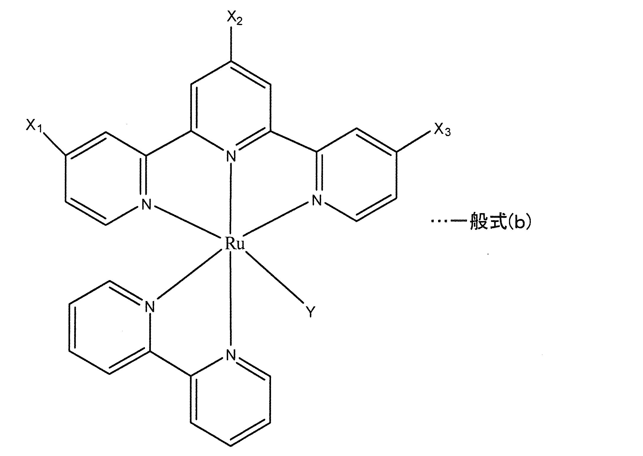
- Examples of the dye having one thiocyanate group described in JP-A-2005-162718 include metal complexes represented by the following general formula (b).
- at least one of X 1 to X 3 may be a linking group such as a carboxyl group or an ammonium carboxylate group, at least one may be an alkyl group having 8 to 40 carbon atoms, and the rest Any hydrogen can be used.
- Y is a thiocyanate group.
- the dye used in the present invention may be a second metal complex having two or more bipyridyl groups and no thiocyanate group. If the dye used in the present invention is the second metal complex, the portion other than the bipyridyl group in the second metal complex interacts with the unshared electron pair of the nitrogen atom in the pyrazole or pyrazole derivative contained in the electrolyte (static It is considered that an attractive force based on the electric interaction) occurs. Moreover, since the 2nd metal complex does not have a thiocyanate group, the fall of the said interaction by a thiocyanate group can be suppressed.
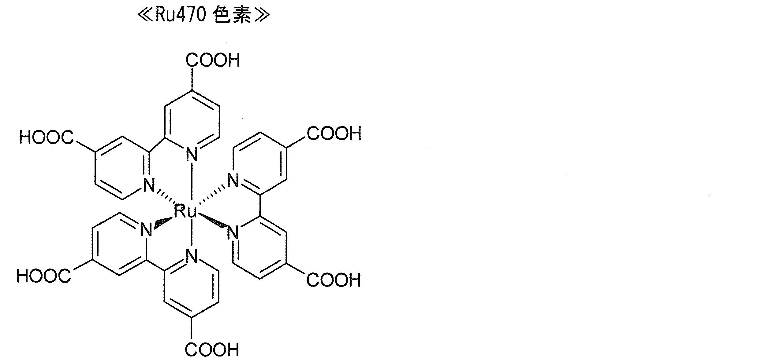
- Examples of the second metal complex include organic dyes typified by commercially available Ru470 (manufactured by Solaronix) or dyes having no thiocyanate group described in JP-A-2005-162717. it can.
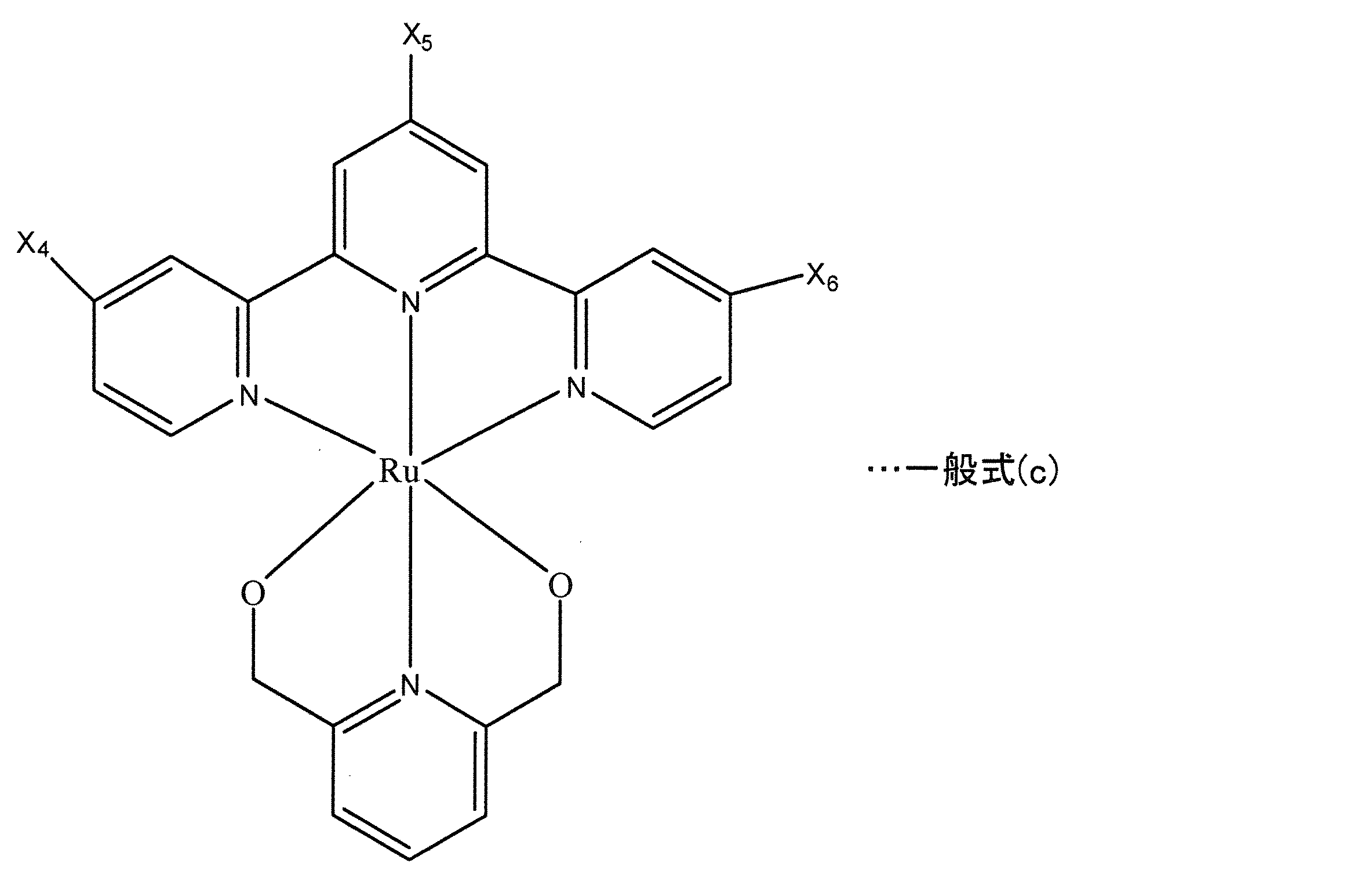
- Examples of the dye having no thiocyanate group described in JP-A-2005-162717 include a dye represented by the following general formula (c).
- at least one of X 4 to X 6 may be a linking group such as a carboxyl group or an ammonium carboxylate group, and the rest may be an alkyl group or hydrogen.
- the dye used in the present invention may be the first metal complex alone, the second metal complex alone, or a mixture of the first metal complex and the second metal complex. There may be.
- the dye used in the present invention is not limited to a metal complex, and may be an organic dye having one thiocyanate group, an organic dye having no thiocyanate group, or a mixture thereof. There may be.
- organic dyes include azo dyes, quinone dyes, quinone imine dyes, quinacridone dyes, squarylium dyes, cyanine dyes, merocyanine dyes, triphenylmethane dyes, xanthene dyes, porphyrin dyes, and perylenes.
- dyes such as indigo dyes, indigo dyes, phthalocyanine dyes, and naphthalocyanine dyes.
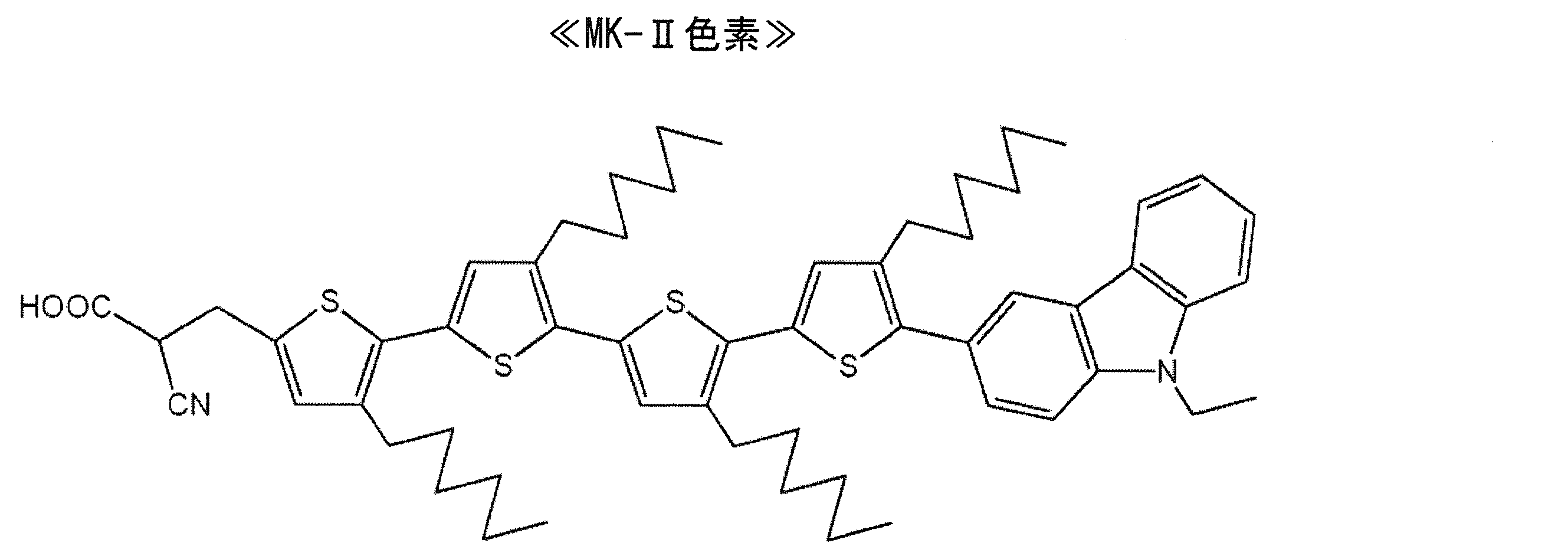
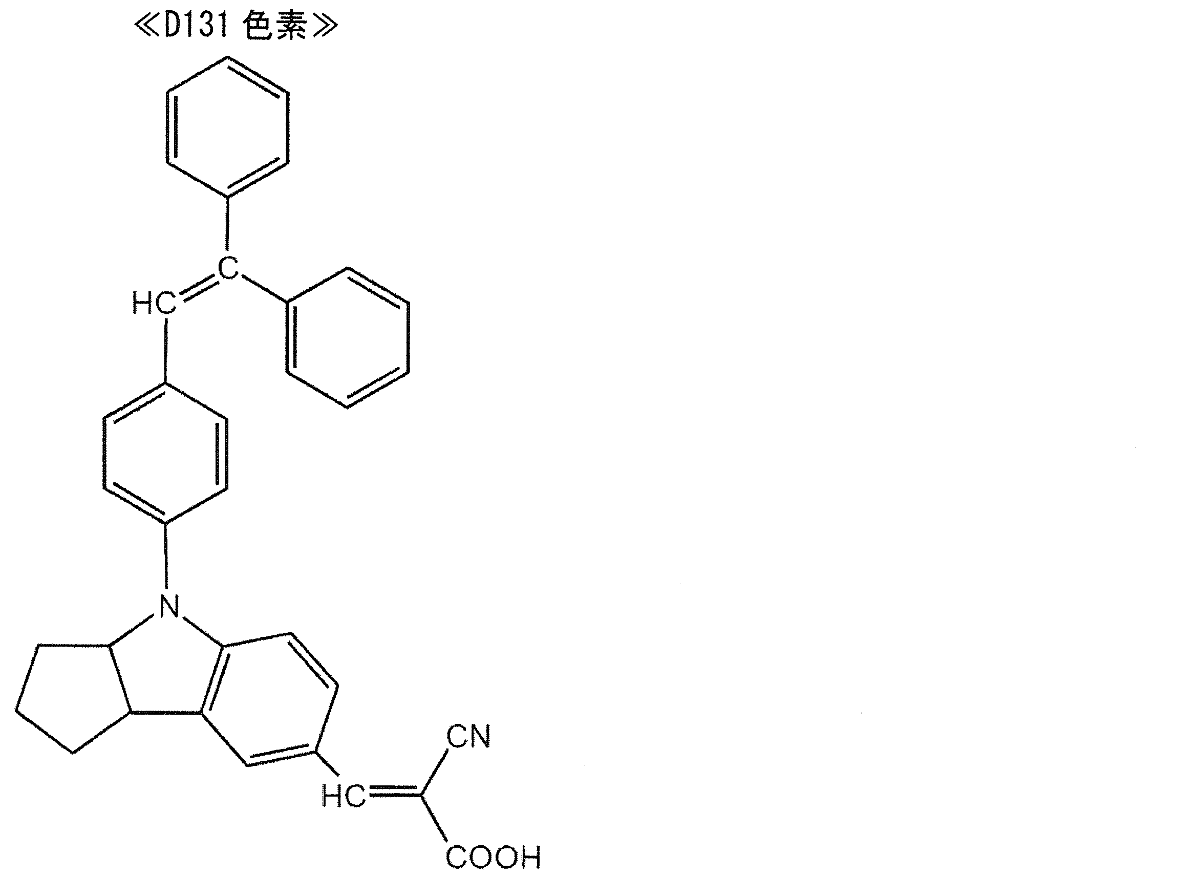
- organic dye having no thiocyanate group examples include MK-II dye (manufactured by Soken Chemical) or D131 dye (manufactured by Mitsubishi Chemical).
- the extinction coefficient of the organic dye is larger than the extinction coefficient of the dye made of the metal complex.
- the central metal is not limited to ruthenium.
- the central metal is not limited to ruthenium.
- ruthenium Cu, Ni, Fe, Co, V, Sn, Si, Ti, Ge, Cr, Zn, Ru, Mg, Al, Pb, Mn, In, Mo, Y, Zr, Nb, Sb, La, W, Pt, Ta, Ir, Pd, Os, Ga, Tb, Eu, Rb, Bi, Se, As, Sc, Ag, Cd, Hf, Re, Au, Ac, Tc or Te may be used.
- the dye used in the present invention may be a phthalocyanine metal complex dye having one thiocyanate group, or may be a phthalocyanine metal complex dye having no thiocyanate group, or one thiocyanate group. It may be a ruthenium-based metal complex dye or a ruthenium-based metal complex dye having no thiocyanate group. Among them, the dye used in the present invention is preferably a ruthenium metal complex dye having one thiocyanate group or a ruthenium metal complex dye having no thiocyanate group.
- the dye contains carboxylic acid group, carboxylic acid anhydride group, alkoxy group, hydroxyl group, hydroxyalkyl group, sulfonic acid group, ester group, mercapto group in the molecule.
- it preferably has an interlock group such as a phosphonyl group, and more preferably has a carboxylic acid group or a carboxylic anhydride group.
- the interlock group provides an electrical bond that facilitates the transfer of electrons between the excited state of the dye and the conduction band of the semiconductor material.
- the amount of dye adsorbed to the porous semiconductor layer is preferably 1 ⁇ 10 ⁇ 8 mol / cm 2 or more and 1 ⁇ 10 ⁇ 6 mol / cm 2 or less, preferably 5 ⁇ 10 ⁇ 8 mol / cm 2 or more and 5 ⁇ 10. More preferably, it is ⁇ 7 mol / cm 2 . If the amount of dye adsorbed is less than 1 ⁇ 10 ⁇ 8 mol / cm 2 , the photoelectric conversion efficiency may be reduced. On the other hand, if the adsorption amount of the dye exceeds 1 ⁇ 10 ⁇ 6 mol / cm 2 , the open circuit voltage may be lowered.
- the amount of dye adsorbed is 1 ⁇ 10 ⁇ 8 mol / cm 2 or more and 1 ⁇ 10 ⁇ 6 mol / cm 2 or less, it is possible to prevent a decrease in photoelectric conversion efficiency and a decrease in release voltage.
- the total adsorbed amount of the dye preferably satisfies the above range.
- the method shown next is mentioned as a measuring method of the adsorption amount of the pigment
- the electrolyte is filled between the photoelectric conversion layer 3 and the counter electrode 8.
- the charge transport layer 4 filled with the electrolyte exists between the photoelectric conversion layer 3 and the counter electrode 8.
- the electrolyte is preferably filled also in the porous semiconductor layer of the photoelectric conversion layer 3.
- an electrolyte containing a conductive polymer or a redox species can be used.
- the highest occupied orbital level of the dye is preferably lower than the Fermi level of the electrolyte (specifically, the redox species) or its redox level. .
- the electrolyte containing a conductive polymer is not particularly limited as long as it is an electrolyte generally used for a battery or a solar battery.
- a conductive polymer for example, a hole transport material such as polyvinyl carbazole or triphenylamine may be used, an electron transport material such as a fullerene derivative or tetranitrofluorenone may be used, or a conductive property such as polypyrrole.
- a polymer may be used, and an inorganic p-type semiconductor such as copper iodide, copper thiocyanate, or nickel oxide may be used.
- the electrolyte containing the redox species is not particularly limited as long as it is an electrolyte generally used for a battery or a solar battery.
- I ⁇ / I 3 ⁇ system, Br 2 ⁇ / Br 3 ⁇ system, Fe 2 + / Fe 3+ system, Na 2 S x / Na 2 S system, (SeCN) 2 / SeCN ⁇ system are used.
- I ⁇ / I 3 ⁇ type redox species examples include metal iodides such as lithium iodide (LiI), sodium iodide (NaI), potassium iodide (KI), and calcium iodide (CaI 2 ).
- metal iodides such as lithium iodide (LiI), sodium iodide (NaI), potassium iodide (KI), and calcium iodide (CaI 2 ).
- I 2 tetraethylammonium iodide
- TPAI tetrapropylammonium iodide
- TBAI tetrabutylammonium iodide
- THAI tetrahexylammonium iodide
- a combination of tetraalkylammonium salt and iodine may be used.
- Examples of the redox species of Br 2 ⁇ / Br 3 ⁇ include, for example, metal bromides such as lithium bromide (LiBr), sodium bromide (NaBr), potassium bromide (KBr), or calcium bromide (CaBr 2 ) A combination with bromine can be used.
- metal bromides such as lithium bromide (LiBr), sodium bromide (NaBr), potassium bromide (KBr), or calcium bromide (CaBr 2 )
- Fe 2+ / Fe 3+ series redox species for example, a combination of iron chloride (II) and iron chloride (III) may be used, or K 3 Fe (CN) 6 and K 4 Fe ( CN) 6 may be used in combination.
- As the (SCN) 2 / SCN ⁇ -based redox species for example, a combination of Pb (SCN) 2 and NaSCN can be used.
- the electrolyte solvent examples include carbonate compounds such as propylene carbonate, nitrile compounds such as acetonitrile, alcohols such as ethanol, water, and aprotic polar substances. Among these, it is particularly preferable to use a carbonate compound or a nitrile compound. These solvents can be used alone or in combination of two or more.
- An additive may be added to the electrolyte as necessary.
- a nitrogen-containing aromatic compound such as t-butylpyridine (TBP) may be used, dimethylpropylimidazole iodide (DMPII), methylpropylimidazole iodide (MPII), ethylmethylimidazoleioio.
- TBP t-butylpyridine
- DMPII dimethylpropylimidazole iodide
- MPII methylpropylimidazole iodide
- EMII dye
- EII ethylimidazole iodide
- HMII hexylmethylimidazole iodide
- the concentration of the redox species in the electrolyte is, for example, preferably 0.001 to 1.5 mol / L, and more preferably 0.01 to 0.7 mol / L.
- the electrolyte further contains at least one of pyrazole and a pyrazole derivative.
- the unshared electron pair of the nitrogen atom in the pyrazole or the pyrazole derivative interacts with the dye used in the present invention, and deterioration of the dye or the like due to heat is prevented.
- the heat resistance of the photoelectric conversion element 10 is remarkably improved, and for example, a decrease in photoelectric conversion efficiency due to heat is suppressed.
- At least one of the hydrogen atoms constituting the pyrazole is an atom other than a hydrogen atom or an arbitrary atomic group (hereinafter, “an atom other than a hydrogen atom or an arbitrary atomic group” is referred to as a “substituent”. It may be substituted by (sometimes).
- examples of atoms other than hydrogen atoms include F, Cl, Br, and I.
- the atomic group may be an alkyl group such as a methyl group, an ethyl group, a propyl group, or a butyl group, an atomic group containing these alkyl groups, an amino group, a phenyl group, a thiophene group, or It may be other than an alkyl group such as a methoxyphenyl group.
- the pyrazole derivative may be one in which one or two hydrogen atoms constituting the pyrazole are substituted with a substituent, and the hydrogen atom constituting the pyrazole is at least a methyl group, an ethyl group, a propyl group or a butyl group.
- the pyrazole derivative is preferably one in which the hydrogen atom at the 1-position of the pyrazole ring is not substituted.
- pyrazole derivative examples include 1-methylpyrazole, 3-methylpyrazole, 3,5-dimethylpyrazole, 3,5-diisopropylpyrazole, 3-amino-5-methylpyrazole, and the like.
- the electrolyte preferably contains at least one of pyrazole and a pyrazole derivative of 0.01 mol / L or more and 10 mol / L or less, and more preferably contains at least one of the pyrazole or the pyrazole derivative of 0.05 mol / L or more and 5 mol / L or less. If the content of at least one of pyrazole and pyrazole derivative in the electrolyte is less than 0.01 mol / L%, it is difficult for the pigment and pyrazole to interact with each other, and thus the degradation of the pigment due to heat is caused. There is.
- electrolyte when the content exceeds 10 mol / L, there may be a problem that pyrazole or a pyrazole derivative is difficult to dissolve in a solvent.
- electrolyte when electrolyte contains a pyrazole and 1 or more types of pyrazole derivatives, it is preferable that the total content of the pyrazole and 1 or more types of pyrazole derivative in electrolyte fills the said range. The same can be said when the electrolyte does not contain pyrazole but contains two or more types of pyrazole derivatives.
- the second conductive layer 6 and the catalyst layer 5 are preferably formed in order on the second support substrate 7, and the catalyst layer 5 is preferably opposed to the photoelectric conversion layer 3. .
- the configuration of the second support substrate 7 is preferably the same as that of the support substrate 1, and the configuration of the second conductive layer 6 is preferably the same as that of the conductive layer 2.
- the second conductive layer 6 also functions as the catalyst layer 5, for example, when the second conductive layer 6 also has a function of activating the oxidation-reduction reaction of the electrolyte, the counter electrode 8 is provided with the catalyst layer 5. Any one of the second conductive layer 6 and the second conductive layer 6 may be provided.
- the material constituting the catalyst layer 5 is not particularly limited as long as it is a material that can generally be used for the catalyst layer of the photoelectric conversion element.
- Examples of the material constituting the catalyst layer 5 include platinum, carbon black, ketjen black, carbon nanotube, or fullerene.
- the form of the catalyst layer 5 is not particularly limited, and examples thereof include a dense film shape, a porous film shape, and a cluster shape.
- the catalyst layer 5 can be formed on the second conductive layer 6 by a known method such as sputtering, thermal decomposition of chloroplatinic acid, or electrodeposition. .
- the thickness of the catalyst layer 5 is preferably about 0.5 nm to 1000 nm, for example.
- the catalyst layer 5 made of carbon such as carbon black, ketjen black, carbon nanotube or fullerene, for example, carbon is dispersed in a solvent to form a paste, and the paste is then subjected to screen printing or the like. It is preferable to apply on the second conductive layer 6.
- the sealing portion 9 has a function of holding the transparent electrode substrate 11 and the counter electrode 8, a function of preventing leakage of the charge transport layer 4, a function of absorbing a fallen object or stress (impact), and a transparent electrode substrate when used over a long period of time.
- 11 and the counter electrode 8 have a function of absorbing the deflection acting on each of them.
- the material which comprises the sealing part 9 will not be specifically limited if it is a material which can generally be used for the sealing part of a photoelectric conversion element, and can exhibit the said function.
- a material include an ultraviolet curable resin or a thermosetting resin, and specifically include a silicone resin, an epoxy resin, a polyisobutylene resin, a hot melt resin, a glass frit, and the like.
- the sealing part 9 may be formed using these alone, or the sealing part 9 may be formed by stacking two or more kinds of these materials in two or more layers.
- the sealing part 9 When forming the sealing part 9 made of silicone resin, epoxy resin or glass frit, the sealing part 9 can be formed using a dispenser. When forming the sealing part 9 which consists of hot-melt resin, the sealing part 9 can be formed by making the hole patterned in the sheet-like hot-melt resin.
- a transparent electrode substrate 11 having a conductive layer 2 formed on a support substrate 1 is prepared.
- a commercially available transparent electrode substrate may be prepared, or the conductive layer 2 may be formed on the support substrate 1 by a method such as sputtering or thermal CVD.
- the photoelectric conversion layer 3 is formed on the conductive layer 2.
- the method for forming the photoelectric conversion layer 3 is not particularly limited.
- the porous semiconductor layer can be formed by any one of the following methods (i) to (iv). Among the following (i) to (iv), it is preferable to use the screen printing method shown in the following (i). Accordingly, a relatively thick porous semiconductor layer tends to be manufactured at low cost.
- a paste containing fine particles made of a semiconductor material is applied on the conductive layer 2 by a screen printing method or an ink jet method and then baked.
- a porous semiconductor layer is formed on the conductive layer 2 using a desired source gas by a CVD method or an MOCVD method.
- a solution in which the dye is dissolved (hereinafter referred to as “dye adsorption solution”) is prepared. It is preferable to use at least one of the compounds listed in the above ⁇ Dye> as the dye.
- the solvent of the dye adsorption solution for example, at least one of a carbonate compound such as propylene carbonate, a nitrile compound such as acetonitrile, an alcohol such as ethanol, water, an aprotic polar substance, or the like can be used.
- the concentration of the dye in the dye adsorption solution is preferably adjusted as appropriate depending on the kind of the dye and the solvent.
- the concentration of the dye in the dye adsorption solution is preferably high, for example, 5 ⁇ 10 ⁇ 4 mol / L or more. preferable.
- a colorless hydrophobic compound such as a steroid compound having a carboxyl group may be co-adsorbed.
- the transparent electrode substrate 11 on which the porous semiconductor layer is formed is immersed in the dye adsorption solution.
- the dye in the dye adsorption solution is adsorbed to the porous semiconductor layer.
- immersion conditions are adjusted suitably.
- the second conductive layer 6 and the catalyst layer 5 are sequentially formed on the second support substrate 7.
- a method for forming the second conductive layer 6 the same method as the method for forming the conductive layer 2 can be used.
- an electrolyte containing at least one of pyrazole and a pyrazole derivative is prepared. Specifically, the electrolyte described in ⁇ Electrolyte> may be prepared.
- the sealing portion 9 is arranged so as to surround the periphery of the porous semiconductor layer on which the dye is adsorbed.
- the transparent electrode substrate 11 and the counter electrode 8 are arranged so that the porous semiconductor layer and the catalyst layer 5 of the counter electrode 8 face each other, the transparent electrode substrate 11 and the counter electrode 8 are fixed by the sealing portion 9. Thereafter, an electrolyte is injected from a hole previously formed in the transparent electrode substrate 11 or the counter electrode 8 into a region surrounded by the sealing portion 9. Thereafter, when the hole is closed, the photoelectric conversion element shown in FIG. 1 is manufactured.
- the photoelectric conversion elements according to the present invention are connected in series. Thereby, the solar cell module which the performance degradation by the heat
- the thickness of each layer was measured using a surface roughness / contour shape measuring instrument (trade name: Surfcom 1400A, manufactured by Tokyo Seimitsu Co., Ltd.).
- Examples 1 to 7> (Formation of photoelectric conversion layer)
- a commercially available titanium oxide paste (manufactured by Solaronix, trade name Ti-Nanoxide D / SP, average particle size 13 nm) is applied to a glass plate (manufactured by Nippon Sheet Glass Co., Ltd., this glass plate is a fluorine-doped SnO 2 film (Transparent conductive film) is applied).
- a glass plate manufactured by Nippon Sheet Glass Co., Ltd., this glass plate is a fluorine-doped SnO 2 film (Transparent conductive film) is applied.
- baking was performed at 500 ° C. for 40 minutes. A series of these steps were performed twice to obtain a titanium oxide film (porous semiconductor layer) having a thickness of 12 ⁇ m.
- the glass plate on which the titanium oxide film was formed was immersed in the dye adsorption solution at room temperature for 80 hours.
- the glass plate immersed in the dye adsorption solution was washed with ethanol and then dried at about 60 ° C. for about 5 minutes. Thereby, the dye was adsorbed on the titanium oxide film.
- MK-II dye (manufactured by Soken Chemical) is used in Example 1
- D131 dye (Mitsubishi Chemical) is used in Example 2
- the above general formula (b) is used in Example 3.
- X 1 is nC 19 H 39
- X 2 is COOH
- X 3 is nC 19 H 39
- Y is a thiocyanate group.
- Ru470 dye (manufactured by Solaronix)
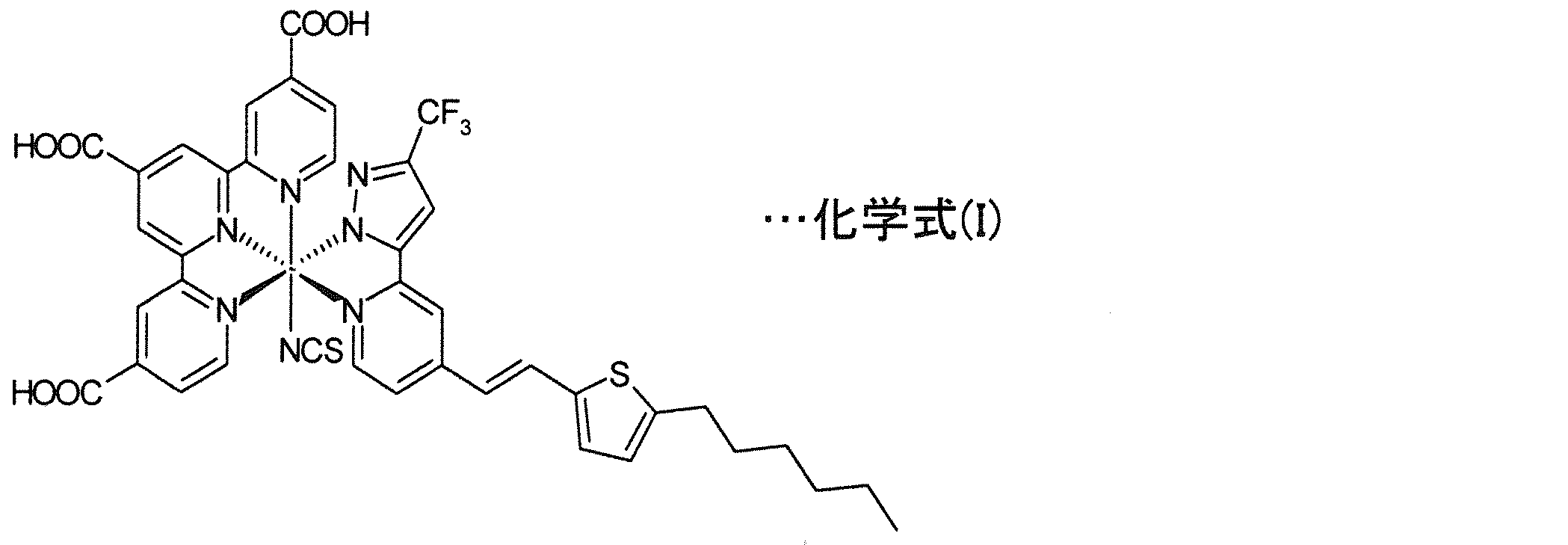
- Example 5 the dye represented by the general formula (c) (X 4 to X 6 are all COOH) was used, and in Example 6, the dye represented by the following chemical formula (I) was used.
- No. 7 a dye represented by the following chemical formula (II) was used. In each example, the dye was dissolved in ethanol so that the dye concentration would be 4 ⁇ 10 ⁇ 4 mol / L.
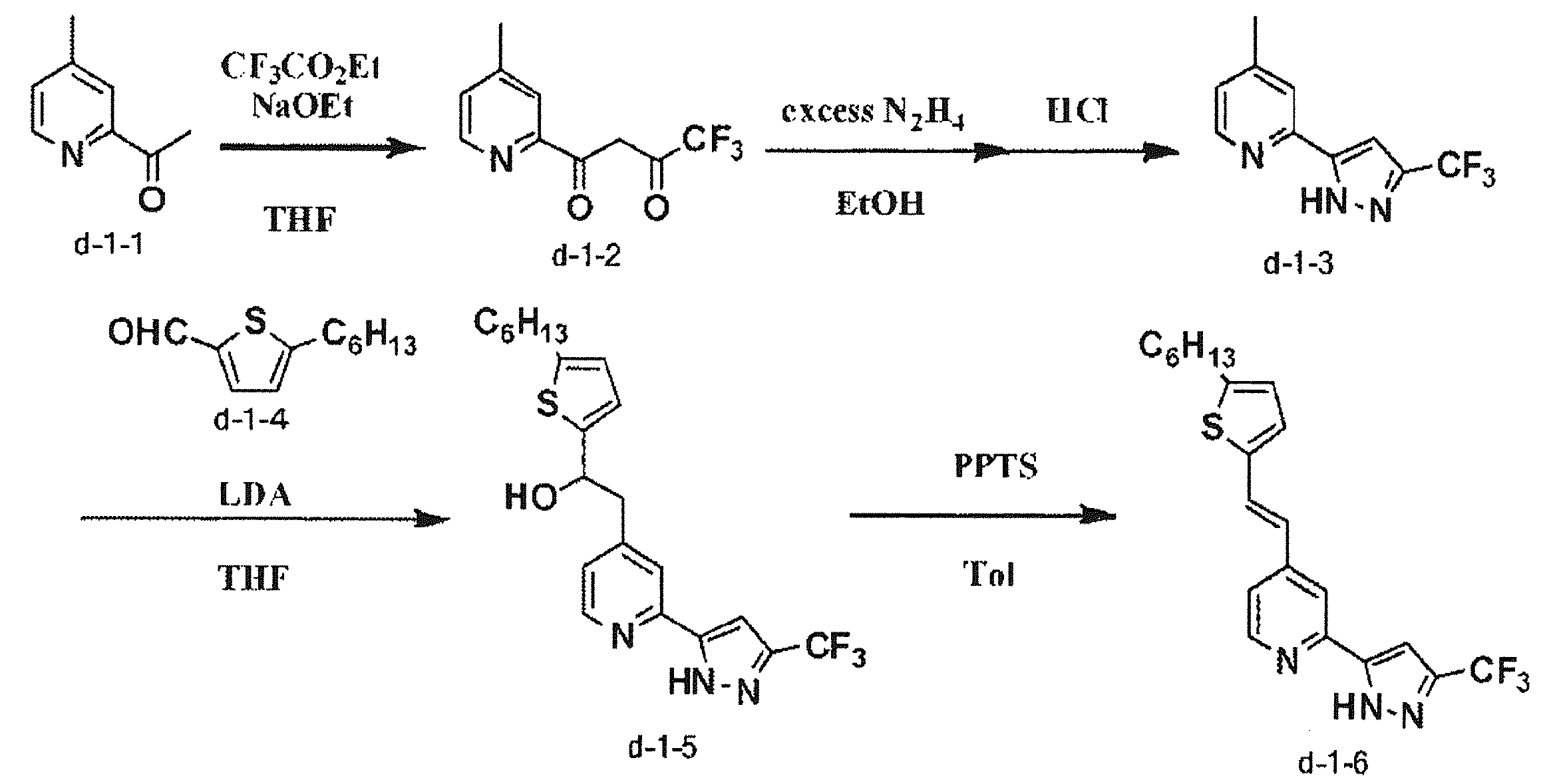
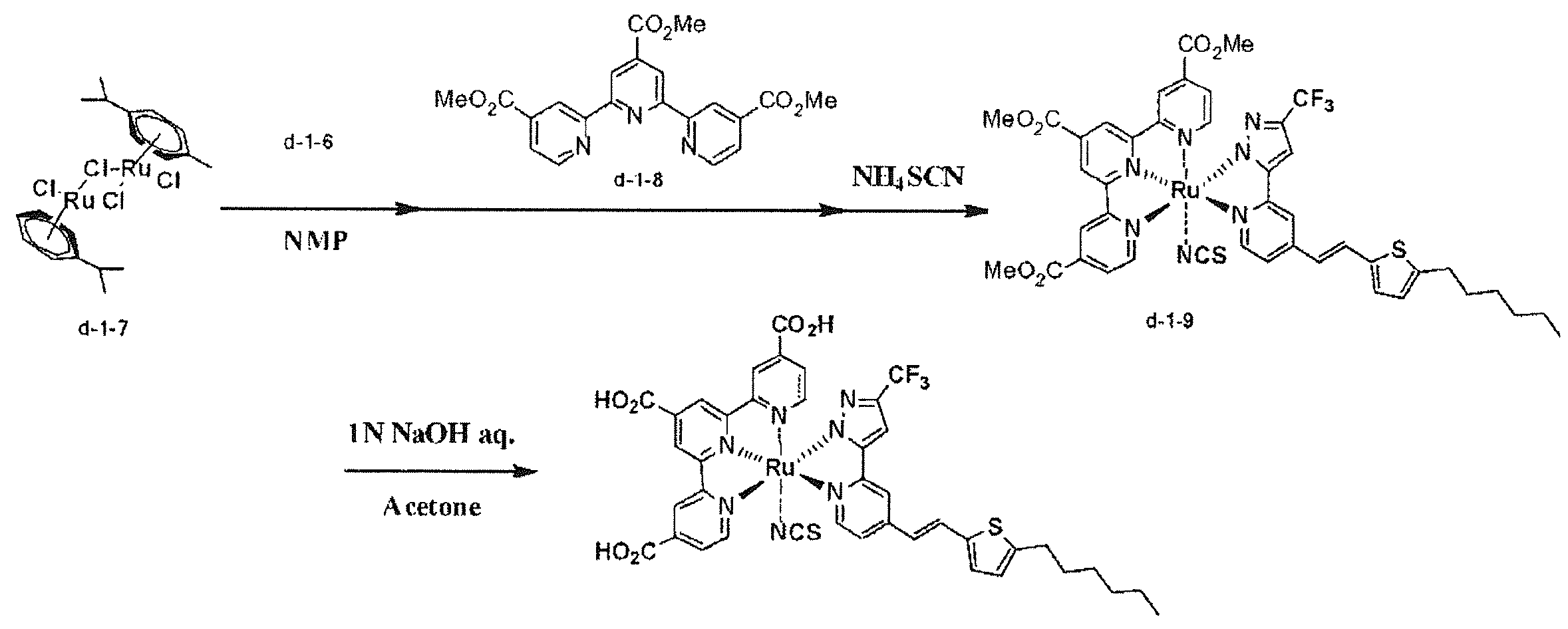
- the dye represented by the chemical formula (I) was obtained according to the method shown in the following scheme.
- (7-1) Preparation of Compound d-1-2 25 g of Compound d-1-1 (2-acetyl-4-methylpyridine) was dissolved in 200 ml of THF (tetrahydrofuran) and stirred at 0 ° C. under a nitrogen atmosphere. 18.9 g of sodium ethoxide was added and stirred for 15 minutes. Thereafter, 28.9 g of ethyl trifluoroacetate was added dropwise and stirred at an external temperature of 70 ° C. for 20 hours. After returning to room temperature, an aqueous ammonium chloride solution was added dropwise, followed by liquid separation, and the organic layer was concentrated to obtain a crude product d-1-2 (72.6 g).
- Table 1 below shows the structure of the dye used in each example.
- Iodine (manufactured by Aldrich) is added to 3-methoxypropionitrile (manufactured by Aldrich) so that the concentration becomes 0.15 mol / L, and dimethylpropylimidazole iodide (DMPII) so that the concentration becomes 0.8 mol / L. , Shikoku Kasei) was added, guanidine thiocyanate (manufactured by Aldrich) was added to a concentration of 0.1 mol / L, and 3-methylpyrazole (manufactured by Aldrich) was added to a concentration of 0.2 mol / L. ) Was added.
- DMPII dimethylpropylimidazole iodide
- the obtained photoelectric conversion element was irradiated with light having an intensity of 1 kW / m 2 (AM1.5 solar simulator), and the photoelectric conversion efficiency was measured. Thereafter, the photoelectric conversion element was held in a constant temperature bath at 85 ° C. for 500 hours, and the change in photoelectric conversion efficiency with time was measured to obtain the photoelectric conversion efficiency retention rate.
- the retention rate of photoelectric conversion efficiency is calculated according to the following formula. It means that the fall of the photoelectric conversion efficiency by a heat
- Retention rate of photoelectric conversion efficiency (photoelectric conversion efficiency after holding photoelectric conversion element in 85 ° C. constant temperature bath for 500 hours) ⁇ (photoelectric conversion before holding photoelectric conversion element in 85 ° C. constant temperature bath) efficiency).
- FIG. 2 shows the results of the retention rate of photoelectric conversion efficiency with respect to the retention time in the constant temperature bath at 85 ° C. in Examples 1 to 7.
- Table 2 below shows the structure of the dye used in each comparative example.
- Examples 8 to 13 Pyrazole, 3,5-dimethylpyrazole, 3-amino-5-methylpyrazole, 3,5-diisopropylpyrazole, 1,3-dimethylpyrazole and 1-methylpyrazole were added to the electrolyte instead of 3-methylpyrazole Except for, the photoelectric conversion elements of Examples 8 to 13 were produced in the same manner as in Example 4 above. In each example, the concentration of pyrazole or pyrazole derivative in the electrolyte was 0.2 mol / L. Then, the retention rate of photoelectric conversion efficiency was calculated
- FIG. 4 shows the results of the retention rate of photoelectric conversion efficiency with respect to the retention time in an 85 ° C. constant temperature bath in Examples 8 to 13.
- Example 14 A photoelectric conversion module of Example 14 was produced by the method described below.
- a 70 mm ⁇ 70 mm ⁇ 4 mm thick glass substrate (manufactured by Nippon Sheet Glass Co., Ltd., glass with SnO 2 film) was prepared.
- the prepared glass substrate was configured by forming a conductive layer 2 made of a SnO 2 film on a glass substrate 1.
- the conductive layer 2 was irradiated with laser light (YAG laser, fundamental wavelength: 1.06 ⁇ m, manufactured by Saishin Shoji Co., Ltd.) to evaporate a part of the conductive layer 2 to form six linear scribes.
- laser light YAG laser, fundamental wavelength: 1.06 ⁇ m, manufactured by Saishin Shoji Co., Ltd.
- a commercially available titanium oxide paste (manufactured by Solaronix, trade name: Ti-Nanoxide D / SP, average particle size: 13 nm) was applied to the glass substrate by a doctor blade method. At this time, since the titanium oxide paste was applied onto the conductive layer 2 so as to sandwich the scribe line, seven coating films having a rectangular shape in plan view were formed on the glass substrate. Next, after preliminary drying at 300 ° C. for 30 minutes, baking was performed at 500 ° C. for 40 minutes. These exemplary steps were performed twice to obtain a titanium oxide film (porous semiconductor layer) having a thickness of 12 ⁇ m.
- a preliminarily prepared zirconium oxide paste was printed on the titanium oxide film using a printer LS-34TVA (manufactured by Neurong Seimitsu Kogyo Co., Ltd.). Then, after preliminary drying at 300 ° C. for 30 minutes, baking was performed at 500 ° C. for 40 minutes. Thereby, a zirconium oxide film (porous insulating layer) having a thickness of 12 ⁇ m was obtained.
- a platinum film was formed at a rate of 0.1 ⁇ / s on the zirconium oxide film (porous insulating layer). The thickness of the formed platinum film was 0.1 ⁇ m.
- a titanium film was formed on the platinum film at 5 ⁇ / s using the same vapor deposition machine. The thickness of the formed titanium film was 1000 nm.
- the laminate thus obtained was immersed in the dye adsorption solution used in Example 6 at room temperature for 80 hours. Thereafter, the laminate was washed with ethanol and then dried at about 60 ° C. for about 5 minutes. Thereby, the pigment
- a cover glass was placed on the laminate in which the dye was adsorbed on the porous semiconductor layer.
- the side surface of the laminate thus formed was sealed with resin 3035B (manufactured by Three Bond Co.). Thereafter, the electrolytic solution of Example 1 was injected from the hole formed in the cover glass, and lead wires were attached to each electrode to obtain a photoelectric conversion module.
- the obtained photoelectric conversion module was irradiated with light having an intensity of 1 kW / m 2 (AM1.5 solar simulator), and the photoelectric conversion efficiency was measured. Thereafter, the photoelectric conversion module was held in a constant temperature bath at 85 ° C. for 500 hours, the change in photoelectric conversion efficiency over time was measured, and the retention rate of photoelectric conversion efficiency was obtained. The obtained retention rate of photoelectric conversion efficiency was 0.95, and in this example, a photoelectric conversion module excellent in retention rate of photoelectric conversion efficiency was obtained.
Landscapes
- Chemical & Material Sciences (AREA)
- Organic Chemistry (AREA)
- Engineering & Computer Science (AREA)
- Power Engineering (AREA)
- Materials Engineering (AREA)
- Chemical Kinetics & Catalysis (AREA)
- Microelectronics & Electronic Packaging (AREA)
- Electrochemistry (AREA)
- General Chemical & Material Sciences (AREA)
- Crystallography & Structural Chemistry (AREA)
- Inorganic Chemistry (AREA)
- Physics & Mathematics (AREA)
- Spectroscopy & Molecular Physics (AREA)
- Hybrid Cells (AREA)
- Photovoltaic Devices (AREA)
Abstract
Description
図1は、本発明に係る光電変換素子の構成の一例を示す断面図である。図1に示す光電変換素子10では、支持基板1上に導電層2と光電変換層3と対極8とが順に設けられており、光電変換層3と対極8との間には電解質が充填されて電荷輸送層4が形成されている。光電変換層3と電荷輸送層4とは封止部9により封止されていることが好ましい。
支持基板1を構成する材料は、一般に光電変換素子の支持基板に使用可能な材料であり且つ本発明の効果を発揮し得る材料であれば、特に限定されない。しかし、光電変換素子の受光面となる部分では光透過性が必要となるため、支持基板1は光透過性を有する材料からなることが好ましい。支持基板1は、たとえば、ソーダガラス、溶融石英ガラス、または結晶石英ガラスなどからなるガラス基板であっても良いし、耐熱性樹脂材料からなる可撓性フィルムであっても良い。ただし、支持基板1は、受光面として使用される場合であっても、少なくとも後述の色素に実効的な感度を有する波長の光を実質的に透過する(当該光の透過率がたとえば80%以上、好ましくは90%以上)ものであれば良く、必ずしも全ての波長領域の光に対して透過性を有する必要はない。
導電層2を構成する材料は、一般に光電変換素子の導電層に使用可能な材料であり且つ本発明の効果を発揮し得る材料であれば、特に限定されない。しかし、導電層2は、光電変換素子10の受光面となるため、光透過性を必要とし、よって光透過性を有する材料からなることが好ましい。導電層2は、たとえば、インジウム錫複合酸化物(ITO)、フッ素がドープされた酸化錫(FTO)または酸化亜鉛(ZnO)などからなることが好ましい。ただし、導電層2は、支持基板1と同じく、少なくとも後述の色素に実効的な感度を有する波長の光を実質的に透過する(当該光の透過率がたとえば80%以上、好ましくは90%以上)ものであれば良く、必ずしも全ての波長領域の光に対して透過性を有する必要はない。
光電変換層3は、半導体材料からなる多孔性半導体層を有する。多孔性半導体層には、1つのチオシアネート基を有する化合物からなる色素およびチオシアネート基を有さない化合物からなる色素のうちの少なくとも1つが吸着されており、好ましくは電解質が充填されている。
多孔性半導体層の形態としては、半導体材料からなるバルク状、粒子状の半導体材料を含む層、または、多数の微細孔が形成された半導体材料からなる膜状などが挙げられるが、多数の微細孔が形成された半導体材料からなる膜状であることが好ましい。これにより、色素の吸着量および電解質の充填量などを十分に確保することができる。
本発明で用いられる色素は、光増感色素として機能し、1つのチオシアネート基を有する化合物からなる色素およびチオシアネート基を有さない化合物からなる色素の少なくとも1つである。

電解質は、光電変換層3と対極8との間に充填されている。別の言い方をすると、電解質が充填されてなる電荷輸送層4が光電変換層3と対極8との間に存在している。電解質は、光電変換層3の多孔性半導体層にも充填されていることが好ましい。
対極8では、第2の導電層6と触媒層5とが第2の支持基板7上に順に形成されていることが好ましく、触媒層5は、光電変換層3と対向していることが好ましい。第2の支持基板7の構成は上記支持基板1と同様であることが好ましく、第2の導電層6の構成は上記導電層2と同様であることが好ましい。なお、第2の導電層6が触媒層5としても機能する場合には、たとえば第2の導電層6が電解質の酸化還元反応を活性化させる働きも有する場合には、対極8は触媒層5および第2の導電層6のうちのどちらか一方を有していれば良い。
封止部9は、透明電極基板11と対極8とを保持する機能、電荷輸送層4の漏えい防止機能、落下物または応力(衝撃)を吸収する機能、および、長期にわたる使用時において透明電極基板11および対極8のそれぞれに作用するたわみなどを吸収する機能を有する。
図1に示す光電変換素子の製造方法を説明する。
(i) スクリーン印刷法またはインクジェット法などによって半導体材料からなる微粒子を含むペーストを導電層2上に塗布した後に焼成する
(ii) CVD法またはMOCVD法などによって、所望の原料ガスを用いて多孔性半導体層を導電層2上に形成する
(iii) 固体原料を用いたPVD法(たとえば蒸着法またはスパッタリング法)などによって、多孔性半導体層を導電層2上に形成する
(iv) ゾル-ゲル法または電気化学的な酸化還元反応を利用した方法などによって、多孔性半導体層を導電層2上に形成する。
本発明に係る太陽電池モジュールでは、本発明に係る光電変換素子(たとえば図1に示す光電変換素子)が直列に接続されている。これにより、熱による性能低下が抑制され且つ光電変換効率が向上した太陽電池モジュールを提供することができる。
(光電変換層の形成)
ドクターブレード法により、市販の酸化チタンペースト(Solaronix社製、商品名Ti-Nanoxide D/SP、平均粒径13nm)を、ガラス板(日本板硝子社製、このガラス板にはフッ素ドープのSnO2膜(透明導電膜)が形成されている)に塗布した。次に、300℃で30分間予備乾燥してから、500℃で40分間焼成した。これらの一連の工程を2回行なって、厚さが12μmの酸化チタン膜(多孔性半導体層)を得た。

(7-1) 化合物d-1-2の調製
化合物d-1-1(2-アセチル-4-メチルピリジン)25gをTHF(テトラヒドロフラン)200mlに溶解し、窒素雰囲気下で0℃で攪拌しながらナトリウムエトキシド18.9gを添加し、15分間、攪拌した。その後、トリフルオロ酢酸エチル28.9gを滴下し、外設70℃で20時間、攪拌した。室温に戻した後、塩化アンモニウム水溶液を滴下してから分液し、有機層を濃縮し、粗精製物d-1-2(72.6g)を得た。
72.6gの化合物d-1-2をエタノール220mlに溶解し、窒素雰囲気下で室温で攪拌しながらヒドラジン1水和物5.6mlを添加し、外設90℃で12時間加熱した。その後、濃塩酸5mlを添加し、1時間攪拌した。濃縮後、重曹水150mlと酢酸エチル150mlとで抽出・分液後、有機層を濃縮した。アセトニトリルで再結晶し、化合物d-1-3(31.5g)を得た。
ジイソプロピルアミン4.1gとテトラヒドロフラン30mlとを窒素雰囲気下で-40℃で攪拌しながら1.6Mのn-ブチルリチウムヘキサン溶液を23.1ml滴下した後、2時間、攪拌した。その後、化合物d-1-3(4.0g)を添加し、0℃で80分攪拌した後、化合物d-1-4(3.45g)をテトラヒドロフラン15mlに溶解した溶液を滴下した。その後、0℃で80分攪拌し、室温で5時間攪拌した。その後、塩化アンモニウム溶液を添加し、酢酸エチルで抽出・分液した。有機層を濃縮し、シリカゲルカラムクロマトグラフィーで精製後、化合物d-1-5(5.7g)を得た。
化合物d-1-5(5.0g)とPPTS(ピリジニウムパラトルエンスルホン酸)5.9gとをトルエン50mlに加え、窒素雰囲気下で5時間、加熱還流を行った。濃縮後、飽和重曹水と塩化メチレンとで分液を行い、有機層を濃縮した。得られた結晶をメタノールと塩化メチレンとで再結晶後、化合物d-1-6(4.3g)を得た。
MS-ESI m/z=404.2(M-H)+
(7-5) 化合物d-1-9の調製
化合物d-1-7(1.22g)と化合物d-1-6(1.62g)とをNMP(N-メチルピロリドン)150mlに加え、窒素雰囲気下で70℃で3時間攪拌した。その後、化合物d-1-8(1.63g)を加え、160℃で8時間加熱攪拌した。その後、チオシアン酸アンモニウム(10.7g)を加え、160℃で8時間攪拌した。濃縮後、水を加え、ろ過した。ろ物をシリカゲルカラムクロマトグラフィーで精製した後、アセトン30mlと1N水酸化ナトリウム水溶液40mlとの混合溶媒に加え、外設65℃で24時間攪拌した。室温に戻し、塩酸でpHを3に調整し、析出物をろ過し、上記化学式(I)で表わされる色素(粗精製物、3.3g)を得た。
MS-ESI m/z=928.1(M-H)+
得られた色素について、340μmol/lテトラブチルアンモニウムヒドロキシドメタノール溶媒で色素濃度が17μmol/lとなるように調製し、分光吸収測定を行ったところ、最大吸収波長は521nmであった。


3-メトキシプロピオニトリル(Aldrich製)に、濃度が0.15mol/Lとなるようにヨウ素(Aldrich製)を添加し、濃度が0.8mol/Lとなるようにジメチルプロピルイミダゾールアイオダイド(DMPII、四国化成製)を添加し、濃度が0.1mol/Lとなるようにグアニジンチオシアナート(Aldrich製)を添加し、濃度が0.2mol/Lとなるように3-メチルピラゾール(Aldrich製)を添加した。
上記(光電変換層の形成)で用いたガラス板とは別に、ガラス板(日本板硝子社製、このガラス板にはフッ素ドープのSnO2膜(透明導電膜)が形成されている)をもう一枚用意した。蒸着機(機種名:ei-5、アルバック社製)を用いて、準備したガラス板(日本板硝子社製)上に白金膜を0.1Å/sで形成した。形成された白金膜の厚さは0.1μmであった。
短絡防止のためのスペーサーを挟んで、白金膜と多孔性半導体層とを重ねた。間隙から電解質を注入して、白金膜と多孔性半導体層とを重ねることにより形成された積層体の側面を樹脂(スリーボンド社製の「31X-101C」)でシールした。そして、ガラス板上に形成されているフッ素ドープのSnO2膜にリード線を取り付けた。これにより、光電変換素子が得られた。
(光電変換効率の保持率)=(光電変換素子を85℃の恒温槽内に500時間保持した後における光電変換効率)÷(光電変換素子を85℃の恒温槽内に保持する前の光電変換効率)。
3-メチルピラゾールを添加することなく電解質を調製したことを除いては上記実施例1および上記実施例4と同様の方法にしたがって、比較例1および比較例2の光電変換素子をそれぞれ製造した。その後、上記方法にしたがって光電変換効率の保持率を求めた。結果を図3に示す。図3には、比較例1~8における85℃の恒温槽内での保持時間に対する光電変換効率の保持率の結果を示す。
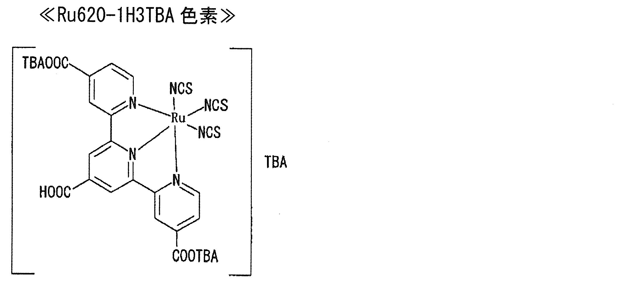
Ru620-1H3TBA色素(Solaronix社製)およびRu535-bis-TBA色素(Solaronix社製)を色素として用いたことを除いては上記比較例1と同様の方法にしたがって、比較例3および比較例4の光電変換素子をそれぞれ製造した。その後、上記方法にしたがって光電変換効率の保持率を求めた。結果を図3に示す。

<比較例5>
上記下記化学式(I)で表される色素を用いたことを除いては上記比較例1と同様の方法にしたがって、比較例5の光電変換素子を製造した。その後、上記方法にしたがって光電変換効率の保持率を求めた。結果を図3に示す。
N-メチルベンズイミダゾール、t-ブチルピリジンおよび1、3-ジメチルイミダゾールを添加して電解質を調製したことを除いては上記比較例5と同様の方法にしたがって、比較例6~8の光電変換素子をそれぞれ製造した。その後、上記方法にしたがって光電変換効率の保持率を求めた。結果を図3に示す。

3-メチルピラゾールの代わりに、ピラゾール、3,5-ジメチルピラゾール、3-アミノ-5-メチルピラゾール、3,5-ジイソプロピルピラゾール、1,3-ジメチルピラゾールおよび1-メチルピラゾールを電解質に添加したことを除いては上記実施例4と同様の方法にしたがって、実施例8~13の光電変換素子をそれぞれ製造した。各実施例では、電解質におけるピラゾールまたはピラゾール誘導体の濃度を0.2mol/Lとした。その後、上記方法にしたがって光電変換効率の保持率を求めた。図4には、実施例8~13における85℃の恒温槽内での保持時間に対する光電変換効率の保持率の結果を示す。
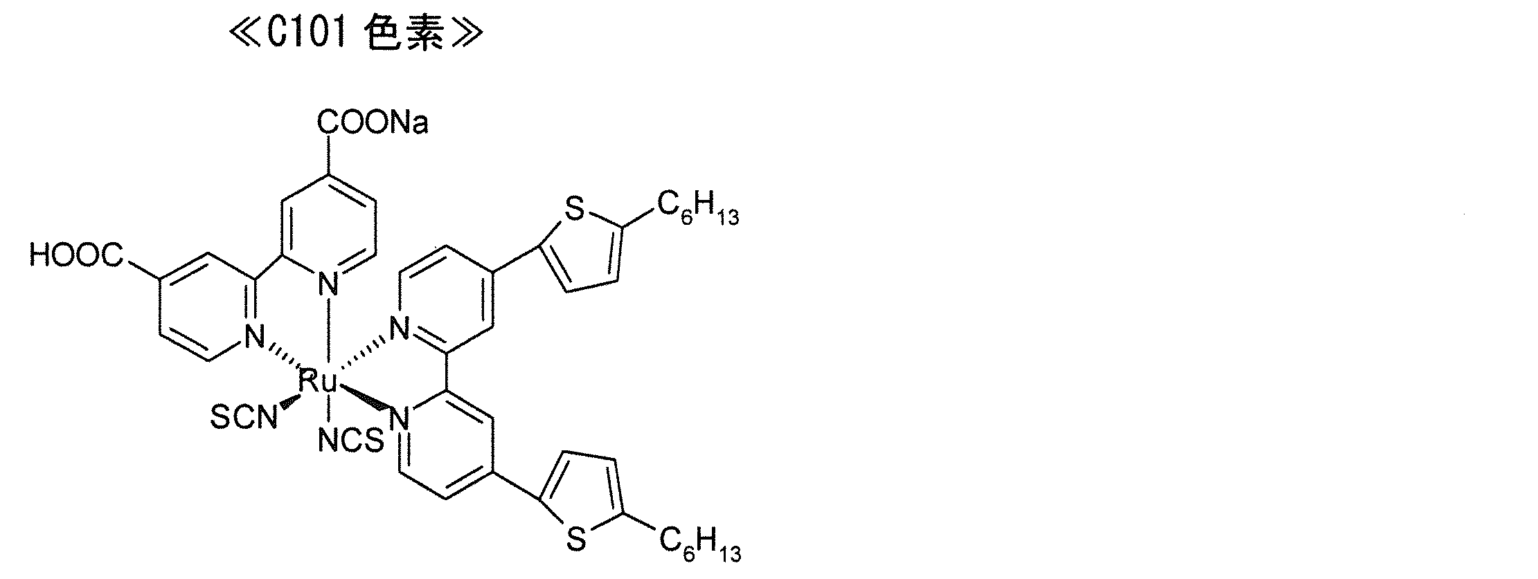
Ru620-1H3TBA色素(Solaronix社製)、Ru535-bis-TBA色素(Solaronix社製)、C101色素(Solaronix社製)およびCYC-B1色素(Solaronix社製)を色素として用いたことを除いては上記実施例1と同様にして、比較例9~12の光電変換素子をそれぞれ製造した。その後、上記方法にしたがって光電変換効率の保持率を求めた。図5には、比較例9~12における85℃の恒温槽内での保持時間に対する光電変換効率の保持率の結果を示す。

以下に示す方法で実施例14の光電変換モジュールを製造した。
Claims (5)
- 導電層と光電変換層と対極とが設けられ、電解質が少なくとも前記光電変換層に充填されている光電変換素子であって、
前記光電変換層では、1つのチオシアネート基を有する化合物からなる色素およびチオシアネート基を有さない化合物からなる色素のうちの少なくとも1つが、半導体材料からなる多孔性半導体層に吸着されており、
前記電解質は、ピラゾールおよびピラゾール誘導体の少なくとも1つを含む光電変換素子。 - 前記色素は、ターピリジル基を有し、1つ以下のチオシアネート基を有する第1の金属錯体である請求項1に記載の光電変換素子。
- 前記色素は、2つ以上のビピリジル基を有し、チオシアネート基を有さない第2の金属錯体である請求項1に記載の光電変換素子。
- 前記ピラゾール誘導体は、前記ピラゾールを構成する水素原子のうちの1つまたは2つが水素原子以外の原子または原子団により置換されたものである請求項1~3のいずれかに記載の光電変換素子。
- 前記ピラゾール誘導体は、前記ピラゾールを構成する水素原子がメチル基、エチル基、プロピル基およびブチル基の少なくとも1つにより置換されたものである請求項1~4のいずれかに記載の光電変換素子。
Priority Applications (4)
| Application Number | Priority Date | Filing Date | Title |
|---|---|---|---|
| JP2014552042A JP6224003B2 (ja) | 2012-12-14 | 2013-12-10 | 光電変換素子 |
| US14/649,376 US20160217936A1 (en) | 2012-12-14 | 2013-12-10 | Photoelectric conversion element |
| EP13863260.9A EP2933874B1 (en) | 2012-12-14 | 2013-12-10 | Photoelectric conversion element |
| US15/672,476 US20170338050A1 (en) | 2012-12-14 | 2017-08-09 | Photoelectric conversion element |
Applications Claiming Priority (2)
| Application Number | Priority Date | Filing Date | Title |
|---|---|---|---|
| JP2012-273636 | 2012-12-14 | ||
| JP2012273636 | 2012-12-14 |
Related Child Applications (2)
| Application Number | Title | Priority Date | Filing Date |
|---|---|---|---|
| US14/649,376 A-371-Of-International US20160217936A1 (en) | 2012-12-14 | 2013-12-10 | Photoelectric conversion element |
| US15/672,476 Continuation-In-Part US20170338050A1 (en) | 2012-12-14 | 2017-08-09 | Photoelectric conversion element |
Publications (1)
| Publication Number | Publication Date |
|---|---|
| WO2014092066A1 true WO2014092066A1 (ja) | 2014-06-19 |
Family
ID=50934354
Family Applications (1)
| Application Number | Title | Priority Date | Filing Date |
|---|---|---|---|
| PCT/JP2013/083045 Ceased WO2014092066A1 (ja) | 2012-12-14 | 2013-12-10 | 光電変換素子 |
Country Status (4)
| Country | Link |
|---|---|
| US (1) | US20160217936A1 (ja) |
| EP (1) | EP2933874B1 (ja) |
| JP (2) | JP6224003B2 (ja) |
| WO (1) | WO2014092066A1 (ja) |
Cited By (2)
| Publication number | Priority date | Publication date | Assignee | Title |
|---|---|---|---|---|
| WO2016148099A1 (ja) * | 2015-03-17 | 2016-09-22 | 富士フイルム株式会社 | 光電変換素子、色素増感太陽電池、ルテニウム錯体色素および色素溶液 |
| WO2016148098A1 (ja) * | 2015-03-17 | 2016-09-22 | 富士フイルム株式会社 | 光電変換素子、色素増感太陽電池、金属錯体色素、金属錯体色素混合物および色素溶液 |
Families Citing this family (7)
| Publication number | Priority date | Publication date | Assignee | Title |
|---|---|---|---|---|
| KR20170033325A (ko) * | 2014-07-30 | 2017-03-24 | 세키스이가가쿠 고교가부시키가이샤 | 태양 전지의 제조 방법 |
| US20170243698A1 (en) * | 2016-02-22 | 2017-08-24 | Ricoh Company, Ltd. | Photoelectric conversion element |
| TWM528479U (zh) * | 2016-05-17 | 2016-09-11 | 位速科技股份有限公司 | 無線射頻辨識裝置 |
| US10210999B2 (en) * | 2016-12-27 | 2019-02-19 | Imam Abdulrahman Bin Faisal University | Dye-sensitized solar cell including a semiconducting nanocomposite |
| JP7295957B2 (ja) * | 2019-07-26 | 2023-06-21 | シャープ株式会社 | 色素増感太陽電池 |
| JP2022075064A (ja) * | 2020-11-06 | 2022-05-18 | 株式会社東芝 | 光電変換素子、塗布液、塗布方法、及び、塗布装置 |
| CN115074760B (zh) * | 2022-06-28 | 2023-11-03 | 阜阳师范大学 | 5-氨基吡唑-4-硫氰酸酯类化合物的电化学合成方法 |
Citations (13)
| Publication number | Priority date | Publication date | Assignee | Title |
|---|---|---|---|---|
| JPH01220380A (ja) | 1988-02-12 | 1989-09-04 | Gebr Sulzer Ag | 光電気化学電池・その製法及び使用法 |
| JP2003331936A (ja) | 2002-05-13 | 2003-11-21 | National Institute Of Advanced Industrial & Technology | ピリジン及び/又はピリジン系化合物を含む電解質溶液を用いた光電変換素子及びそれを用いた色素増感型太陽電池 |
| JP2004047229A (ja) | 2002-07-10 | 2004-02-12 | National Institute Of Advanced Industrial & Technology | アミノピリジン系化合物を含む電解質溶液を用いた光電変換素子及びそれを用いた色素増感型太陽電池 |
| JP2005120042A (ja) | 2003-10-17 | 2005-05-12 | Sharp Corp | ルテニウム錯体、それを用いた色素増感酸化物半導体電極および色素増感太陽電池 |
| JP2005162717A (ja) | 2003-12-05 | 2005-06-23 | Sharp Corp | 金属錯体およびそれを用いた色素増感太陽電池 |
| JP2005162718A (ja) | 2003-12-05 | 2005-06-23 | Sharp Corp | 金属錯体およびそれを用いた色素増感太陽電池 |
| JP2005216490A (ja) | 2004-01-27 | 2005-08-11 | National Institute Of Advanced Industrial & Technology | 光電変換素子及びそれを用いた色素増感型太陽電池 |
| JP2006134615A (ja) | 2004-11-02 | 2006-05-25 | Erekuseru Kk | 光電変換素子 |
| JP2007194039A (ja) | 2006-01-18 | 2007-08-02 | Sharp Corp | 色素増感太陽電池および色素増感太陽電池モジュール |
| JP2012146632A (ja) * | 2010-12-21 | 2012-08-02 | Sony Corp | 色素、色素増感光電変換素子、電子機器および建築物 |
| JP2012195280A (ja) * | 2011-03-02 | 2012-10-11 | Sony Corp | 光電変換素子、光電変換素子の製造方法、電子機器および建築物 |
| JP2012199096A (ja) * | 2011-03-22 | 2012-10-18 | Sony Corp | 光電変換素子の製造方法および電子装置の製造方法 |
| JP2012243436A (ja) * | 2011-05-17 | 2012-12-10 | Sony Corp | 光電変換素子およびその製造方法ならびに電子機器 |
Family Cites Families (5)
| Publication number | Priority date | Publication date | Assignee | Title |
|---|---|---|---|---|
| KR100589323B1 (ko) * | 2004-02-03 | 2006-06-14 | 삼성에스디아이 주식회사 | 광 흡수파장대가 확장된 염료감응 태양전지 및 그 제조방법 |
| US8759521B2 (en) * | 2009-04-10 | 2014-06-24 | National Tsing Hua University | Panchromatic photosensitizers and dye-sensitized solar cell using the same |
| TWI428343B (zh) * | 2010-05-14 | 2014-03-01 | Nat Univ Tsing Hua | 無硫氰酸根配基的光敏錯合物及敏化染料太陽能電池 |
| TWI419878B (zh) * | 2010-09-28 | 2013-12-21 | Nat Univ Tsing Hua | 雜配、雙三芽釕錯合物以及敏化染料太陽能電池製備 |
| KR101137379B1 (ko) * | 2010-11-23 | 2012-04-20 | 삼성에스디아이 주식회사 | 염료감응 태양전지용 겔형 전해질 및 이를 포함하는 염료감응 태양전지 |
-
2013
- 2013-12-10 US US14/649,376 patent/US20160217936A1/en not_active Abandoned
- 2013-12-10 EP EP13863260.9A patent/EP2933874B1/en not_active Not-in-force
- 2013-12-10 JP JP2014552042A patent/JP6224003B2/ja not_active Expired - Fee Related
- 2013-12-10 WO PCT/JP2013/083045 patent/WO2014092066A1/ja not_active Ceased
-
2017
- 2017-10-03 JP JP2017193448A patent/JP2018019092A/ja active Pending
Patent Citations (13)
| Publication number | Priority date | Publication date | Assignee | Title |
|---|---|---|---|---|
| JPH01220380A (ja) | 1988-02-12 | 1989-09-04 | Gebr Sulzer Ag | 光電気化学電池・その製法及び使用法 |
| JP2003331936A (ja) | 2002-05-13 | 2003-11-21 | National Institute Of Advanced Industrial & Technology | ピリジン及び/又はピリジン系化合物を含む電解質溶液を用いた光電変換素子及びそれを用いた色素増感型太陽電池 |
| JP2004047229A (ja) | 2002-07-10 | 2004-02-12 | National Institute Of Advanced Industrial & Technology | アミノピリジン系化合物を含む電解質溶液を用いた光電変換素子及びそれを用いた色素増感型太陽電池 |
| JP2005120042A (ja) | 2003-10-17 | 2005-05-12 | Sharp Corp | ルテニウム錯体、それを用いた色素増感酸化物半導体電極および色素増感太陽電池 |
| JP2005162717A (ja) | 2003-12-05 | 2005-06-23 | Sharp Corp | 金属錯体およびそれを用いた色素増感太陽電池 |
| JP2005162718A (ja) | 2003-12-05 | 2005-06-23 | Sharp Corp | 金属錯体およびそれを用いた色素増感太陽電池 |
| JP2005216490A (ja) | 2004-01-27 | 2005-08-11 | National Institute Of Advanced Industrial & Technology | 光電変換素子及びそれを用いた色素増感型太陽電池 |
| JP2006134615A (ja) | 2004-11-02 | 2006-05-25 | Erekuseru Kk | 光電変換素子 |
| JP2007194039A (ja) | 2006-01-18 | 2007-08-02 | Sharp Corp | 色素増感太陽電池および色素増感太陽電池モジュール |
| JP2012146632A (ja) * | 2010-12-21 | 2012-08-02 | Sony Corp | 色素、色素増感光電変換素子、電子機器および建築物 |
| JP2012195280A (ja) * | 2011-03-02 | 2012-10-11 | Sony Corp | 光電変換素子、光電変換素子の製造方法、電子機器および建築物 |
| JP2012199096A (ja) * | 2011-03-22 | 2012-10-18 | Sony Corp | 光電変換素子の製造方法および電子装置の製造方法 |
| JP2012243436A (ja) * | 2011-05-17 | 2012-12-10 | Sony Corp | 光電変換素子およびその製造方法ならびに電子機器 |
Non-Patent Citations (5)
| Title |
|---|
| KUAN-LIN WU ET AL.: "Development of thiocyanate-free, charge-neutral Ru(II) sensitizers for dye-sensitized solar cells", CHEMICAL COMMUNICATIONS, vol. 46, no. 28, 2010, pages 5124 - 5126, XP055257270 * |
| KUAN-LIN WU ET AL.: "Thiocyanate-Free Ru(II) Sensitizers with a 4,4'-Dicarboxyvinyl-2,2'-bipyridine Anchor for Dye-Sensitized Solar Cells", ADVANCED FUNCTIONAL MATERIALS, vol. 23, no. 18, 13 May 2013 (2013-05-13), pages 2285 - 2294, XP001582794 * |
| KUSAMA, H. ET AL.: "Influence of pyrazole derivatives in I /I3 redox electrolyte solution on Ru(II)-dye-sensitized Ti02 solar cell performance", SOLAR ENERGY MATERIALS AND SOLAR CELLS, vol. 85, no. 3, 31 January 2005 (2005-01-31), pages 333 - 344, XP025333185 * |
| KUSAMA, H. ET AL.: "Theoretical studies of charge-transfer complexes 12 with pyrazoles, and implications on the dye-sensitized solar cell performance", JOURNAL OF PHOTOCHEMISTRY AND PHOTOBIOLOGY A: CHEMISTRY, vol. 187, no. 2-3, 23 March 2007 (2007-03-23), pages 233 - 241, XP005934356 * |
| See also references of EP2933874A4 |
Cited By (4)
| Publication number | Priority date | Publication date | Assignee | Title |
|---|---|---|---|---|
| WO2016148099A1 (ja) * | 2015-03-17 | 2016-09-22 | 富士フイルム株式会社 | 光電変換素子、色素増感太陽電池、ルテニウム錯体色素および色素溶液 |
| WO2016148098A1 (ja) * | 2015-03-17 | 2016-09-22 | 富士フイルム株式会社 | 光電変換素子、色素増感太陽電池、金属錯体色素、金属錯体色素混合物および色素溶液 |
| JPWO2016148099A1 (ja) * | 2015-03-17 | 2017-09-14 | 富士フイルム株式会社 | 光電変換素子、色素増感太陽電池、ルテニウム錯体色素および色素溶液 |
| JPWO2016148098A1 (ja) * | 2015-03-17 | 2017-11-02 | 富士フイルム株式会社 | 光電変換素子、色素増感太陽電池、金属錯体色素、金属錯体色素混合物および色素溶液 |
Also Published As
| Publication number | Publication date |
|---|---|
| JP6224003B2 (ja) | 2017-11-01 |
| JP2018019092A (ja) | 2018-02-01 |
| EP2933874B1 (en) | 2021-02-24 |
| US20160217936A1 (en) | 2016-07-28 |
| EP2933874A1 (en) | 2015-10-21 |
| EP2933874A4 (en) | 2016-07-27 |
| JPWO2014092066A1 (ja) | 2017-01-12 |
Similar Documents
| Publication | Publication Date | Title |
|---|---|---|
| JP6224003B2 (ja) | 光電変換素子 | |
| US9406446B2 (en) | Dye-sensitized solar cell, method of producing the same, and dye-sensitized solar cell module | |
| US9607772B2 (en) | Porous electrode, dye-sensitized solar cell, and dye-sensitized solar cell module | |
| US20110197948A1 (en) | Dye-sensitized solar cell and dye-sensitized solar cell module | |
| US10014122B2 (en) | Photoelectric conversion element and photoelectric conversion element module | |
| JP5171810B2 (ja) | 色素増感太陽電池モジュールおよびその製造方法 | |
| JP2014238969A (ja) | 太陽電池 | |
| JP7295957B2 (ja) | 色素増感太陽電池 | |
| JP6104177B2 (ja) | 光電変換素子 | |
| JP5758400B2 (ja) | 色素増感太陽電池モジュールおよびその製造方法 | |
| US20170338050A1 (en) | Photoelectric conversion element | |
| JP5956929B2 (ja) | 光電変換素子およびその製造方法 | |
| JP5313278B2 (ja) | 光電変換素子および光電変換素子モジュール | |
| US10916382B2 (en) | Photoelectric conversion element and photoelectric conversion element module | |
| US20140366933A1 (en) | Photoelectric conversion element | |
| WO2014057942A1 (ja) | 光電変換素子およびその製造方法ならびに光電変換モジュール | |
| WO2015049983A1 (ja) | 光電変換装置および光電変換装置の製造方法 |
Legal Events
| Date | Code | Title | Description |
|---|---|---|---|
| 121 | Ep: the epo has been informed by wipo that ep was designated in this application |
Ref document number: 13863260 Country of ref document: EP Kind code of ref document: A1 |
|
| WWE | Wipo information: entry into national phase |
Ref document number: 2013863260 Country of ref document: EP |
|
| ENP | Entry into the national phase |
Ref document number: 2014552042 Country of ref document: JP Kind code of ref document: A |
|
| WWE | Wipo information: entry into national phase |
Ref document number: 14649376 Country of ref document: US |
|
| NENP | Non-entry into the national phase |
Ref country code: DE |