WO2014097724A1 - 粒子検出装置及び粒子検出方法 - Google Patents
粒子検出装置及び粒子検出方法 Download PDFInfo
- Publication number
- WO2014097724A1 WO2014097724A1 PCT/JP2013/077883 JP2013077883W WO2014097724A1 WO 2014097724 A1 WO2014097724 A1 WO 2014097724A1 JP 2013077883 W JP2013077883 W JP 2013077883W WO 2014097724 A1 WO2014097724 A1 WO 2014097724A1
- Authority
- WO
- WIPO (PCT)
- Prior art keywords
- light
- detection
- particle
- detector
- scattered light
- Prior art date
- Legal status (The legal status is an assumption and is not a legal conclusion. Google has not performed a legal analysis and makes no representation as to the accuracy of the status listed.)
- Ceased
Links
Images





Classifications
-
- G—PHYSICS
- G01—MEASURING; TESTING
- G01N—INVESTIGATING OR ANALYSING MATERIALS BY DETERMINING THEIR CHEMICAL OR PHYSICAL PROPERTIES
- G01N15/00—Investigating characteristics of particles; Investigating permeability, pore-volume or surface-area of porous materials
- G01N15/10—Investigating individual particles
- G01N15/14—Optical investigation techniques, e.g. flow cytometry
- G01N15/1429—Signal processing
-
- G—PHYSICS
- G01—MEASURING; TESTING
- G01N—INVESTIGATING OR ANALYSING MATERIALS BY DETERMINING THEIR CHEMICAL OR PHYSICAL PROPERTIES
- G01N15/00—Investigating characteristics of particles; Investigating permeability, pore-volume or surface-area of porous materials
- G01N15/10—Investigating individual particles
- G01N15/14—Optical investigation techniques, e.g. flow cytometry
- G01N15/1434—Optical arrangements
-
- G—PHYSICS
- G01—MEASURING; TESTING
- G01N—INVESTIGATING OR ANALYSING MATERIALS BY DETERMINING THEIR CHEMICAL OR PHYSICAL PROPERTIES
- G01N15/00—Investigating characteristics of particles; Investigating permeability, pore-volume or surface-area of porous materials
- G01N15/10—Investigating individual particles
- G01N15/14—Optical investigation techniques, e.g. flow cytometry
- G01N15/1456—Optical investigation techniques, e.g. flow cytometry without spatial resolution of the texture or inner structure of the particle, e.g. processing of pulse signals
- G01N15/1459—Optical investigation techniques, e.g. flow cytometry without spatial resolution of the texture or inner structure of the particle, e.g. processing of pulse signals the analysis being performed on a sample stream
-
- G—PHYSICS
- G01—MEASURING; TESTING
- G01N—INVESTIGATING OR ANALYSING MATERIALS BY DETERMINING THEIR CHEMICAL OR PHYSICAL PROPERTIES
- G01N15/00—Investigating characteristics of particles; Investigating permeability, pore-volume or surface-area of porous materials
- G01N15/10—Investigating individual particles
- G01N15/14—Optical investigation techniques, e.g. flow cytometry
- G01N15/1484—Optical investigation techniques, e.g. flow cytometry microstructural devices
-
- G—PHYSICS
- G01—MEASURING; TESTING
- G01N—INVESTIGATING OR ANALYSING MATERIALS BY DETERMINING THEIR CHEMICAL OR PHYSICAL PROPERTIES
- G01N21/00—Investigating or analysing materials by the use of optical means, i.e. using sub-millimetre waves, infrared, visible or ultraviolet light
- G01N21/17—Systems in which incident light is modified in accordance with the properties of the material investigated
- G01N21/47—Scattering, i.e. diffuse reflection
- G01N21/49—Scattering, i.e. diffuse reflection within a body or fluid
-
- G—PHYSICS
- G01—MEASURING; TESTING
- G01N—INVESTIGATING OR ANALYSING MATERIALS BY DETERMINING THEIR CHEMICAL OR PHYSICAL PROPERTIES
- G01N15/00—Investigating characteristics of particles; Investigating permeability, pore-volume or surface-area of porous materials
- G01N2015/0042—Investigating dispersion of solids
- G01N2015/0053—Investigating dispersion of solids in liquids, e.g. trouble
-
- G—PHYSICS
- G01—MEASURING; TESTING
- G01N—INVESTIGATING OR ANALYSING MATERIALS BY DETERMINING THEIR CHEMICAL OR PHYSICAL PROPERTIES
- G01N15/00—Investigating characteristics of particles; Investigating permeability, pore-volume or surface-area of porous materials
- G01N15/10—Investigating individual particles
- G01N2015/1006—Investigating individual particles for cytology
Definitions
- the present technology relates to a particle detection apparatus and a particle detection method for optically detecting particles. More specifically, the present invention relates to a technique for detecting scattered light from light-irradiated particles.
- An optical detection method using flow cytometry is used to identify biologically relevant microparticles such as cells, microorganisms, and liposomes.
- Flow cytometry irradiates particles that flow in a single line in a flow path with laser light of a specific wavelength, and detects fluorescence and scattered light emitted from each particle to detect one particle. It is an analysis method that identifies each one.
- the target particle when the target particle is a cell, information such as its shape, size, surface state, nucleus formation and presence can be obtained by detecting forward scattered light (FS).
- FS forward scattered light
- the forward scattered light from the target particles is detected by a photodetector such as a photodiode.
- the photodetector detects light other than forward scattered light such as irradiation light (hereinafter also referred to as zero-order light). Light is also incident.
- a light scattering method in which a light receiving means is formed by a plurality of photoelectric elements and an addition processing means for adding the outputs of the plurality of photoelectric elements is provided.
- a type particle detector (refer to patent documents 1).
- a technique for removing unnecessary light by arranging a light shielding mask on the optical path of scattered light is also proposed.
- Patent Document 2 a microparticle measuring apparatus in which an optical filter is arranged instead of a light shielding mask has been proposed (see Patent Document 2).
- Patent Document 1 is intended to improve the S / N ratio, which is the ratio between the amount of signal (signal) and the amount of noise (noise), by increasing the amount of scattered light received.
- S / N ratio is the ratio between the amount of signal (signal) and the amount of noise (noise)
- the main object of the present disclosure is to provide a particle detection apparatus and a particle detection method that can detect scattered light with high accuracy.
- the particle detection device includes a light irradiation unit that irradiates light to particles, and a scattered light detection unit that detects scattered light emitted from the light-irradiated particles, the scattered light detection unit, A first detection unit that detects the scattered light, a second detection unit that detects a light component derived from light irradiated on the particles, and the first detection unit based on a signal detected by the second detection unit And a signal processing unit for removing noise components from the signal detected in step (b).
- the first detector and the second detector may be provided in one photodetector.
- the first detection unit can be provided around the second detection unit.
- the photodetector may be divided into nine or more regions.
- an irradiation light removing member that blocks a light component derived from the irradiation light may be disposed in front of the photodetector.
- the irradiation light detector and the scattered light detector can be arranged in this order on the optical path of the scattered light.
- An irradiation light removing member that blocks a light component derived from the irradiation light may be disposed between the irradiation light detector and the scattered light detector.
- the said irradiation light detector can also be arrange
- an irradiation light removing member that blocks a light component derived from the irradiation light may be disposed between the mirror and the scattered light detector.
- the signal processing unit may remove a noise component by subtracting a signal obtained by multiplying the detection signal of the second detection unit by a gain value from the detection signal of the first detection unit.
- the scattered light is, for example, forward scattered light.
- the light irradiation unit may irradiate light to particles flowing through the flow path, and the flow path may be formed on a microchip.
- the particle detection method includes a light irradiation step of irradiating light to a particle, a scattered light detection step of detecting scattered light emitted from the particle in a first detection unit, and a particle detection method in a second detection unit.
- a noise component may be removed by subtracting a signal obtained by multiplying the detection signal of the second detection unit by a gain value from the detection signal of the first detection unit.
- the gain value can be set based on a detection signal in the first detection unit and a detection signal in the second detection unit when light is irradiated in a state where the particles do not exist.
- the scattered light since the noise component is removed from the scattered light detection signal, the scattered light can be detected with high accuracy.
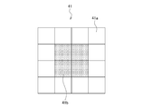
- FIG. 6 is a diagram showing a positional relationship between a detection region of the photodetector 41 shown in FIG.
- First Embodiment Example of a particle detection device in which two types of detection regions are provided in a photodetector
- Modification of First Embodiment Example of Particle Detection Device in which Zero-Order Light Removal Member is Arranged in Front of Photodetector
- Second Embodiment Example of particle detection apparatus including two types of photodetectors
- First Modification of Second Embodiment Example of Particle Detection Device Comprising Zeroth Order Photodetector and Zeroth Order Light Removal Member
- Second Modification of Second Embodiment Example of Particle Detection Device in which Zero-Order Photodetector is Provided Outside Light Path of Scattered Light
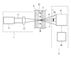
- FIG. 1 is a diagram schematically showing the configuration of the particle detection apparatus of the present embodiment.
- the particle detection apparatus according to the present embodiment includes a light irradiation unit 1 that irradiates light to a microparticle 3 and a scattered light detection unit that detects scattered light 7 emitted from the light-irradiated microparticle 3. 4 is provided.
- the light irradiation unit 1 is provided with a light source 11 that generates excitation light 5 such as laser light, and a lens 12 that condenses the excitation light 5 generated by the light source 11 toward the fine particles 3. Then, for example, the excitation light 5 is irradiated to the microparticles 3 flowing through the flow path 21 formed in the microchip 2.
- the microchip 2 is provided with a flow path 21 through which the microparticles 3 can flow, and a sample liquid containing, for example, the microparticles 3 to be detected is introduced into the flow path 21.
- the microchip 2 can be formed of glass or various plastics (PP, PC, COP, PDMS, etc.).
- the material of the microchip 2 is not particularly limited, but it is desirable to use a material that is transparent to the excitation light 5 irradiated from the light irradiation unit 1 and has a small optical error.
- the microchip 2 can be formed by wet etching or dry etching of a glass substrate, or by nanoimprinting, injection molding, or machining of a plastic substrate. And the microchip 2 can be formed by sealing the board
- the “microparticles 3” detected by the particle detection apparatus of the present embodiment widely include living body-related microparticles such as cells, microorganisms, and ribosomes, or synthetic particles such as latex particles, gel particles, and industrial particles. .
- Biologically relevant microparticles include chromosomes, ribosomes, mitochondria, organelles (cell organelles), etc. that make up various cells.
- the cells include plant cells, animal cells, blood cells, and the like.
- microorganisms include bacteria such as Escherichia coli, viruses such as tobacco mosaic virus, and fungi such as yeast.
- the biologically relevant microparticles may include biologically relevant polymers such as nucleic acids, proteins, and complexes thereof.
- Industrial particles include those formed of organic polymer materials, inorganic materials, metal materials, and the like.
- organic polymer material polystyrene, styrene / divinylbenzene, polymethyl methacrylate, or the like can be used.
- inorganic material glass, silica, a magnetic material, etc. can be used.
- metal material for example, gold colloid and aluminum can be used.
- shape of these fine particles is generally spherical, it may be non-spherical, and the size and mass are not particularly limited.
- the scattered light detection unit 4 detects the scattered light 7 emitted from the microparticles 3 irradiated with the excitation light 5, and is provided with a photodetector 41, a signal processing unit 42, and the like.
- the light detector 41 is composed of a photodiode and the like, and together with the forward scattered light 7 emitted from the light-irradiated microparticles 3, the light component other than the forward scattered light 7 such as the excitation light 5 (0th order light 6). Is detected.
- FIG. 2 is a schematic diagram showing a detection region of the photodetector 41. As shown in FIG. 2, the light receiving surface of the photodetector 41 is divided into a zero-order light detection region 41 b for detecting zero-order light 6 and a scattered light detection region 41 a for detecting forward scattered light 7.
- the forward scattered light 7 is light scattered at an acute angle ( ⁇ 19 °) with respect to the optical axis of the excitation light 5, the light component around the optical axis in the light incident on the photodetector 41 is mainly 0. It is the next light 6 and hardly contains the forward scattered light 7.
- the light receiving surface of the photodetector 41 has a zero-order light detection region 41b at the center and a scattered light detection region 41a around the center.
- the number of divisions of the light receiving surface of the photodetector 41 is not particularly limited, but is preferably 9 divisions (3 ⁇ 3) or more from the viewpoint of improving the differential effect described later, and is divided into 16 divisions. More preferably (4 ⁇ 4) or more.
- the signal processing unit 42 removes a noise component from the signal detected in the scattered light detection area 41a based on the signal detected in the 0th-order light detection area 41b.
- the light incident on the photodetector 41 includes a wide variety of noises such as drive current noise of the light source 11, noise of laser light as the excitation light 5, and noise received in the optical path. These noises are included in both the 0th-order light (leakage light) 6 and the forward scattered light 7 with the same phase but different levels.
- Equation 1 the processing shown in the following Equation 1 is performed on the signal detected in each region, and the obtained signal is set as a forward scattered light signal.
- the gain value (Gain) in Equation 1 below is based on the detection signal of the scattered light detection region 41a and the detection signal of the 0th-order light detection region 41b when the excitation light 5 is irradiated without passing through the fine particles 3. Is the set value.
- the particle detection apparatus of the present embodiment is provided with other scattered light detection units that detect side scattered light, a fluorescence detection unit that detects fluorescence emitted from the microparticles 3, and the like, as necessary. It may be.
- the operation of the particle detection apparatus of this embodiment that is, a method for detecting the microparticles 3 using the particle content detection apparatus of this embodiment will be described.
- a sample liquid containing, for example, the detection target microparticles 3 is introduced into the flow path 21 provided in the microchip 2.
- the excitation light 5 emitted from the light source 11 is collected by the lens 12 or the like, and irradiated to the microparticles 3 flowing through the flow path 21 of the microchip 2.
- the forward scattered light 7 emitted from the microparticles 3 irradiated with the excitation light 5 is detected by the photodetector 41.
- the zero-order light detection region 41b and the scattered light detection region 41a are provided on the light receiving surface of the photodetector 41, and both are detected.
- FIG. 3A is a diagram showing a signal detected in the scattered light detection region 41a
- FIG. 3B is a diagram showing a signal detected in the 0th-order light detection region 41b.
- FIG. 3A in the scattered light detection area 41a, noise included in the zero-order light 6 and a signal of the forward scattered light 7 are detected.
- FIG. 3B in the 0th-order light detection region 41b, the signal of the forward scattered light 7 is hardly detected, and a noise component mainly included in the 0th-order light 6 is detected.
- the noise caused by the excitation light 5 detected in the scattered light detection area 41a and the noise contained in the 0th-order light 6 detected in the 0th-order light detection area 41b have the same phase, although there is a difference in level. It is. Therefore, in the particle detection device of the present embodiment, the signal processing unit 42 removes noise components from the signal detected in the scattered light detection region 41a based on the signal detected in the 0th-order light detection region 41b.
- FIG. 4 is a diagram illustrating a signal from which noise components have been removed by the signal processing unit 42. As a result, as shown in FIG. 4, only the waveform of the signal substantially derived from the forward scattered light 7 is obtained.
- the gain value used in the processing performed by the signal processing unit 42 is a value adjusted so that the noise of the forward scattered light 7 and the zero-order light 6 becomes zero.
- a sample liquid that does not contain the microparticles 3 is allowed to flow through the flow path 21, and a change in the noise level included in the signal is detected while changing the gain value in that state, and the value is obtained when noise is eliminated.
- noise components are removed from the signal detected in the scattered light detection region 41a based on the signal detected in the 0th-order light detection region 41b.
- the detection accuracy of forward scattered light can be improved.
- grain detection apparatus of this embodiment can remove the low frequency and high frequency noise contained in the leakage light (0th-order light 6) which injects into the scattered light detection area
- this indication is not limited to the case where the microparticle 3 is detected using the microchip 2, It is possible to apply to various particle
- the present technology can be applied not only to forward scattered light but also to detection of other scattered light, and in this case, the same effect can be obtained.
- FIG. 5 is a diagram schematically showing the configuration of the particle detection device of this modification
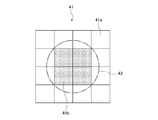
- FIG. 6 is a diagram showing the positional relationship between the detection region of the photodetector 41 and the zero-order light removal member 43. 5 and 6, the same components as those of the particle detection device of the first embodiment described above are denoted by the same reference numerals, and detailed description thereof is omitted.
- a zero-order light removal member 43 that blocks the zero-order light 6 is disposed in front of the photodetector 41.
- the 0th-order light removing member 43 may be a mask or an optical filter that selectively blocks specific light, but is not limited thereto, and can block the 0th-order light 6. Any optical member may be used.
- the 0th-order light removal member 43 is arranged as in this modification. As a result, the intensity of the zero-order light 6 can be lowered. Thereby, even when the signal intensity of the 0th-order light 6 is high, the noise component can be removed and the forward scattered light can be detected with high accuracy.
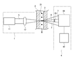
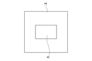
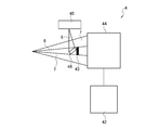
- FIG. 7 is a diagram schematically showing the configuration of the particle detection apparatus of this embodiment
- FIG. 8 is a diagram showing the positional relationship between the detection region of the scattered light detector 44 and the zero-order light detector 45. 7 and 8, the same components as those of the particle detection device of the first embodiment described above are denoted by the same reference numerals, and detailed description thereof is omitted.
- a zero-order light detector 45 that detects zero-order light 6 and a scattered light detector 44 that detects scattered light 7 on the optical path are arranged in this order.
- a commonly used photodetector such as a photodiode can be used as the zero-order light detector 45 and the scattered light detector 44.
- the signal processing unit 42 removes noise components from the signal detected by the scattered light detector 44 based on the signal detected by the zero-order light detector 45. Thereby, the detection accuracy of the forward scattered light can be improved as in the first embodiment described above.
- FIG. 9 is a diagram schematically showing the configuration of the particle detection apparatus of this modification.
- FIG. 10 shows the positional relationship between the detection region of the scattered light detector 44, the zero-order light detector 45, and the zero-order light removal member 43.
- FIG. 9 and FIG. 10 the same components as those of the particle detection devices of the first embodiment and the second embodiment described above are denoted by the same reference numerals, and detailed description thereof is omitted.
- a 0th-order light removal member 43 that blocks the 0th-order light 6 is interposed between the 0th-order light detector 45 and the scattered light detector 44.
- the zero-order light removal member 43 together with the zero-order light detector 45, the noise removal effect can be further enhanced and the detection accuracy of scattered light can be improved.
- the configurations, operations, and effects of the present modification other than those described above are the same as those of the first embodiment, the modification, and the second embodiment described above.
- FIG. 11 is a diagram schematically showing the configuration of the scattered light detection unit 4 of the particle detection device of the present modification.
- the zero-order light detector 45 is arranged outside the optical path, and the optical path of the zero-order light 6 is changed by the mirror 46 arranged on the optical path.
- the light is guided to the photodetector 45.
- the signal processing unit 42 removes noise components from the signal detected by the scattered light detector 44 based on the signal detected by the zero-order light detector 45. Accordingly, it is possible to detect the forward scattered light with high accuracy, as in the above-described modified example.
- a light irradiation unit for irradiating the particles with light;
- a scattered light detector for detecting scattered light emitted from the light-irradiated particles;
- Have The scattered light detection unit A first detector for detecting the scattered light;
- a second detection unit for detecting a light component derived from the irradiation light to the particles;
- a signal processing unit for removing a noise component from the signal detected by the first detection unit based on the signal detected by the second detection unit;
- a particle detection apparatus comprising: (2) The particle detector according to (1), wherein the first detector and the second detector are provided in one photodetector.
- the particle detector according to (2) or (3) wherein the photodetector has a light receiving surface divided into nine or more regions.
- the particle detector according to (1) comprising: a scattered light detector that functions as the first detector; and an irradiation light detector that functions as the second detector.
- the particle detector according to (6) wherein the irradiation light detector and the scattered light detector are arranged in this order on the optical path of the scattered light.
- the signal processing unit removes a noise component by subtracting, from the detection signal of the first detection unit, a signal obtained by multiplying the detection signal of the second detection unit by a gain value (1) to (10).
- a light irradiation step of irradiating the particles with light A scattered light detection step of detecting scattered light emitted from the particles in the first detector; An irradiation light step of detecting a light component derived from the irradiation light on the particles in the second detection unit; A signal processing step of removing a noise component from the signal detected by the first detection unit based on the signal detected by the second detection unit;
- a particle detection method comprising: (16) The particle detection method according to (15), wherein the signal processing step removes a noise component from a detection signal of the first detection unit by subtracting a signal obtained by multiplying the detection signal of the second detection unit by a gain value. .
- the gain value is set based on a detection signal in the first detection unit and a detection signal in the second detection unit when light is irradiated in a state where the particles do not exist.
Landscapes
- Chemical & Material Sciences (AREA)
- General Health & Medical Sciences (AREA)
- Biochemistry (AREA)
- Pathology (AREA)
- Physics & Mathematics (AREA)
- Health & Medical Sciences (AREA)
- Life Sciences & Earth Sciences (AREA)
- Analytical Chemistry (AREA)
- Immunology (AREA)
- General Physics & Mathematics (AREA)
- Dispersion Chemistry (AREA)
- Engineering & Computer Science (AREA)
- Signal Processing (AREA)
- Investigating, Analyzing Materials By Fluorescence Or Luminescence (AREA)
- Investigating Or Analysing Materials By Optical Means (AREA)
Abstract
Description
この粒子検出装置では、前記第1検出部と前記第2検出部とが一の光検出器に設けられていてもよい。
その場合、前記第2検出部の周囲に前記第1検出部を設けることができる。
また、前記光検出器は、受光面が9以上の領域に分割されていてもよい。
更に、前記光検出器の手前に、前記照射光に由来する光成分を遮断する照射光除去部材を配置することもできる。
一方、前記第1検出部として機能する散乱光検出器と、前記第2検出部として機能する照射光検出器と、を有していてもよい。
その場合、前記散乱光の光路上に、前記照射光検出器と前記散乱光検出器をこの順に配置することができる。
また、前記照射光検出器と前記散乱光検出器との間に、前記照射光に由来する光成分を遮断する照射光除去部材が配置されていてもよい。
又は、前記照射光に由来する光成分の光路を変更するミラーを有し、前記照射光検出器を前記散乱光の光路外に配置することもできる。
その場合、前記ミラーと前記散乱光検出器との間に、前記照射光に由来する光成分を遮断する照射光除去部材を配置することもできる。
前記信号処理部は、前記第1検出部の検出信号から、前記第2検出部の検出信号にゲイン値を乗じた信号を減ずることにより、ノイズ成分を除去してもよい。
また、前記散乱光は、例えば前方散乱光である。
更に、前記光照射部は、流路を通流する粒子に光を照射してもよく、前記流路は、マイクロチップに形成されていてもよい。
前記信号処理工程では、前記第1検出部の検出信号から、前記第2検出部の検出信号にゲイン値を乗じた信号を減ずることにより、ノイズ成分を除去してもよい。
また、前記粒子が存在しない状態で光を照射したときの前記第1検出部における検出信号及び第2検出部における検出信号に基づいて前記ゲイン値を設定することもできる。
1.第1の実施形態
(光検出器に2種類の検出領域が設けられている粒子検出装置の例)
2.第1の実施形態の変形例
(光検出器の手前に0次光除去部材が配置された粒子検出装置の例)
3.第2の実施形態
(2種類の光検出器を備える粒子検出装置の例)
4.第2の実施形態の第1変形例
(0次光検出器と0次光除去部材を備える粒子検出装置の例)
5.第2の実施形態の第2変形例
(0次光検出器が散乱光の光路外に設けられている粒子検出装置の例)
[装置の全体構成]
先ず、本開示の第1の実施形態の粒子検出装置について、流路内を通流する微小粒子を検出する場合を例にして説明する。図1は本実施形態の粒子検出装置の構成を模式的に示す図である。図1に示すように、本実施形態の粒子検出装置は、微小粒子3に光を照射する光照射部1と、光照射された微小粒子3から発せられる散乱光7を検出する散乱光検出部4を備えている。
光照射部1には、レーザ光などの励起光5を発生する光源11と、光源11で発生した励起光5を微小粒子3に向けて集光するレンズ12などが設けられている。そして、例えばマイクロチップ2内に形成された流路21内を通流する微小粒子3に励起光5を照射する。
マイクロチップ2には、微小粒子3が通流可能な流路21が設けられており、流路21内に、例えば検出対象の微小粒子3を含むサンプル液が導入される。このマイクロチップ2は、ガラスや各種プラスチック(PP,PC,COP、PDMSなど)により形成することができる。マイクロチップ2の材質は、特に限定されるものではないが、光照射部1から照射される励起光5に対して透過性を有し、光学誤差が少ない材質とすることが望ましい。
本実施形態の粒子検出装置で検出される「微小粒子3」には、細胞、微生物及びリボゾームなどの生体関連微小粒子、又はラテックス粒子、ゲル粒子及び工業用粒子などの合成粒子などが広く含まれる。
散乱光検出部4は、励起光5が照射された微小粒子3から発せられる散乱光7を検出するものであり、光検出器41及び信号処理部42などが設けられている。
光検出器41は、フォトダイオードなどで構成されており、光照射された微小粒子3から発せられる前方散乱光7と共に、励起光5などの前方散乱光7以外の光成分(0次光6)を検出する。図2は光検出器41の検出領域を示す模式図である。図2に示すように、光検出器41の受光面は、0次光6を検出する0次光検出領域41bと、前方散乱光7を検出する散乱光検出領域41aとに分割されている。
信号処理部42は、0次光検出領域41bで検出された信号に基づいて、散乱光検出領域41aで検出された信号からノイズ成分を除去する。ここで、光検出器41に入射する光には、光源11の駆動電流ノイズ、励起光5であるレーザ光のノイズ、光路で受けるノイズなど多種多様のノイズが含まれている。これらのノイズは、レベルは異なるが、同じ位相で、0次光(漏れ光)6及び前方散乱光7の両方に含まれている。

次に、本実施形態の粒子検出装置の動作、即ち、本実施形態の粒子分検出装置を使用して微小粒子3を検出する方法について説明する。本実施形態の粒子検出装置では、マイクロチップ2に設けられた流路21内に、例えば検出対象の微小粒子3を含むサンプル液を導入する。そして、光源11から出射した励起光5をレンズ12などで集光して、マイクロチップ2の流路21内を通流する微小粒子3に照射する。
次に、本開示の第1の実施形態の変形例に係る粒子検出装置について説明する。図5は本変形例の粒子検出装置の構成を模式的に示す図であり、図6は光検出器41の検出領域と0次光除去部材43の位置関係を示す図である。なお、図5及び図6では、前述した第1の実施形態の粒子検出装置の構成要素と同じものには、同じ符号を付し、その詳細な説明は省略する。
次に、本開示の第2の実施形態に係る粒子検出装置について説明する。図7は本実施形態の粒子検出装置の構成を模式的に示す図であり、図8は散乱光検出器44の検出領域と0次光検出器45の位置関係を示す図である。なお、図7及び図8では、前述した第1の実施形態の粒子検出装置の構成要素と同じものには、同じ符号を付し、その詳細な説明は省略する。
次に、本開示の第2の実施形態の第1変形例に係る粒子検出装置について説明する。図9は本変形例の粒子検出装置の構成を模式的に示す図であり、図10は散乱光検出器44の検出領域と0次光検出器45と0次光除去部材43の位置関係を示す図である。なお、図9及び図10では、前述した第1の実施形態及び第2の実施形態の粒子検出装置の構成要素と同じものには、同じ符号を付し、その詳細な説明は省略する。
図7に示す第2の実施形態では、光路上に、0次光検出器45と散乱光検出器44とを配置しているが、本開示はこれに限定されるものではなく、0次光検出器45を光路外に配置することもできる。図11は本変形例の粒子検出装置の散乱光検出部4の構成を模式的に示す図である。
(1)
粒子に光を照射する光照射部と、
光照射された粒子から発せられる散乱光を検出する散乱光検出部と、
を有し、
前記散乱光検出部は、
前記散乱光を検出する第1検出部と、
前記粒子への照射光に由来する光成分をを検出する第2検出部と、
前記第2検出部で検出された信号に基づいて前記第1検出部で検出された信号からノイズ成分を除去する信号処理部と、
を備える粒子検出装置。
(2)
前記第1検出部と前記第2検出部とが一の光検出器に設けられている(1)に記載の粒子検出装置。
(3)
前記第2検出部の周囲に前記第1検出部が設けられている(2)に記載の粒子検出装置。
(4)
前記光検出器は、受光面が9以上の領域に分割されている(2)又は(3)に記載の粒子検出装置。
(5)
前記光検出器の手前に、前記照射光に由来する光成分を遮断する照射光除去部材が配置されている(2)~(4)のいずれかに記載の粒子検出装置。
(6)
前記第1検出部として機能する散乱光検出器と、前記第2検出部として機能する照射光検出器と、を有する(1)に記載の粒子検出装置。
(7)
前記散乱光の光路上に、前記照射光検出器と前記散乱光検出器がこの順に配置されている(6)に記載の粒子検出装置。
(8)
前記照射光検出器と前記散乱光検出器との間に、前記照射光に由来する光成分を遮断する照射光除去部材が配置されている(6)又は(7)に記載の粒子検出装置。
(9)
前記照射光に由来する光成分の光路を変更するミラーを有し、前記照射光検出器は前記散乱光の光路外に配置されている(6)に記載の粒子検出装置。
(10)
前記ミラーと前記散乱光検出器との間に、前記照射光に由来する光成分を遮断する照射光除去部材が配置されている(9)に記載の粒子検出装置。
(11)
前記信号処理部は、前記第1検出部の検出信号から、前記第2検出部の検出信号にゲイン値を乗じた信号を減ずることにより、ノイズ成分を除去する(1)~(10)のいずれかに記載の粒子検出装置。
(12)
前記散乱光が前方散乱光である(1)~(11)のいずれかに記載の粒子検出装置。
(13)
前記光照射部は、流路を通流する粒子に光を照射する(1)~(12)のいずれかに記載の粒子検出装置。
(14)
前記流路は、マイクロチップに形成されている(13)に記載の粒子検出装置。
(15)
粒子に光を照射する光照射工程と、
第1検出部において前記粒子から発せられた散乱光を検出する散乱光検出工程と、
第2検出部において前記粒子への照射光に由来する光成分を検出する照射光工程と、
前記第2検出部で検出された信号に基づいて前記第1検出部で検出された信号からノイズ成分を除去する信号処理工程と、
を有する粒子検出方法。
(16)
前記信号処理工程は、前記第1検出部の検出信号から、前記第2検出部の検出信号にゲイン値を乗じた信号を減ずることにより、ノイズ成分を除去する(15)に記載の粒子検出方法。
(17)
前記粒子が存在しない状態で光を照射したときの前記第1検出部における検出信号及び第2検出部における検出信号に基づいて前記ゲイン値を設定する(16)に記載の粒子検出方法。
Claims (17)
- 粒子に光を照射する光照射部と、
光照射された粒子から発せられる散乱光を検出する散乱光検出部と、
を有し、
前記散乱光検出部は、
前記散乱光を検出する第1検出部と、
前記粒子への照射光に由来する光成分を検出する第2検出部と、
前記第2検出部で検出された信号に基づいて前記第1検出部で検出された信号からノイズ成分を除去する信号処理部と、
を備える粒子検出装置。 - 前記第1検出部と前記第2検出部とが一の光検出器に設けられている請求項1に記載の粒子検出装置。
- 前記第2検出部の周囲に前記第1検出部が設けられている請求項2に記載の粒子検出装置。
- 前記光検出器は、受光面が9以上の領域に分割されている請求項2に記載の粒子検出装置。
- 前記光検出器の手前に、前記照射光に由来する光成分を遮断する照射光除去部材が配置されている請求項2に記載の粒子検出装置。
- 前記第1検出部として機能する散乱光検出器と、前記第2検出部として機能する照射光検出器と、を有する請求項1に記載の粒子検出装置。
- 前記散乱光の光路上に、前記照射光検出器と前記散乱光検出器がこの順に配置されている請求項6に記載の粒子検出装置。
- 前記照射光検出器と前記散乱光検出器との間に、前記照射光に由来する光成分を遮断する照射光除去部材が配置されている請求項7に記載の粒子検出装置。
- 前記照射光に由来する光成分の光路を変更するミラーを有し、前記照射光検出器は前記散乱光の光路外に配置されている請求項6に記載の粒子検出装置。
- 前記ミラーと前記散乱光検出器との間に、前記照射光に由来する光成分を遮断する照射光除去部材が配置されている請求項9に記載の粒子検出装置。
- 前記信号処理部は、前記第1検出部の検出信号から、前記第2検出部の検出信号にゲイン値を乗じた信号を減ずることにより、ノイズ成分を除去する請求項1に記載の粒子検出装置。
- 前記散乱光が前方散乱光である請求項1に記載の粒子検出装置。
- 前記光照射部は、流路を通流する粒子に光を照射する請求項1に記載の粒子検出装置。
- 前記流路は、マイクロチップに形成されている請求項13に記載の粒子検出装置。
- 粒子に光を照射する光照射工程と、
第1検出部において前記粒子から発せられた散乱光を検出する散乱光検出工程と、
第2検出部において前記粒子への照射光に由来する光成分を検出する照射光工程と、
前記第2検出部で検出された信号に基づいて前記第1検出部で検出された信号からノイズ成分を除去する信号処理工程と、
を有する粒子検出方法。 - 前記信号処理工程は、前記第1検出部の検出信号から、前記第2検出部の検出信号にゲイン値を乗じた信号を減ずることにより、ノイズ成分を除去する請求項15に記載の粒子検出方法。
- 前記粒子が存在しない状態で光を照射したときの前記第1検出部における検出信号及び第2検出部における検出信号に基づいて前記ゲイン値を設定する請求項16に記載の粒子検出方法。
Priority Applications (3)
| Application Number | Priority Date | Filing Date | Title |
|---|---|---|---|
| US14/652,433 US9638622B2 (en) | 2012-12-21 | 2013-10-15 | Particle detection apparatus and particle detection method |
| EP13863786.3A EP2937681B1 (en) | 2012-12-21 | 2013-10-15 | Particle detection device and particle detection method |
| JP2014552974A JP6536034B2 (ja) | 2012-12-21 | 2013-10-15 | 粒子検出装置及び粒子検出方法 |
Applications Claiming Priority (2)
| Application Number | Priority Date | Filing Date | Title |
|---|---|---|---|
| JP2012-278881 | 2012-12-21 | ||
| JP2012278881 | 2012-12-21 |
Publications (1)
| Publication Number | Publication Date |
|---|---|
| WO2014097724A1 true WO2014097724A1 (ja) | 2014-06-26 |
Family
ID=50978074
Family Applications (1)
| Application Number | Title | Priority Date | Filing Date |
|---|---|---|---|
| PCT/JP2013/077883 Ceased WO2014097724A1 (ja) | 2012-12-21 | 2013-10-15 | 粒子検出装置及び粒子検出方法 |
Country Status (4)
| Country | Link |
|---|---|
| US (1) | US9638622B2 (ja) |
| EP (1) | EP2937681B1 (ja) |
| JP (1) | JP6536034B2 (ja) |
| WO (1) | WO2014097724A1 (ja) |
Cited By (1)
| Publication number | Priority date | Publication date | Assignee | Title |
|---|---|---|---|---|
| CN107615043A (zh) * | 2015-04-02 | 2018-01-19 | 粒子监测系统有限公司 | 粒子计数仪器中的激光器噪声检测和缓解 |
Families Citing this family (2)
| Publication number | Priority date | Publication date | Assignee | Title |
|---|---|---|---|---|
| CN106950162B (zh) * | 2017-04-12 | 2023-07-21 | 江苏苏净集团有限公司 | 一种颗粒计数方法及系统 |
| KR102450625B1 (ko) * | 2017-08-31 | 2022-10-07 | 서울바이오시스 주식회사 | 검출기 |
Citations (6)
| Publication number | Priority date | Publication date | Assignee | Title |
|---|---|---|---|---|
| JPH1019885A (ja) * | 1996-04-02 | 1998-01-23 | Avl Medical Instr Ag | 濃度測定装置およびその方法 |
| JP2002031594A (ja) | 2000-05-12 | 2002-01-31 | Rion Co Ltd | 光散乱式粒子検出器 |
| JP2002243624A (ja) * | 2001-02-20 | 2002-08-28 | Horiba Ltd | 粒径分布測定装置 |
| JP2005055233A (ja) * | 2003-07-31 | 2005-03-03 | Horiba Ltd | 粒径分布測定装置 |
| JP2012026837A (ja) | 2010-07-22 | 2012-02-09 | Sony Corp | 微小粒子測定装置 |
| JP2012073070A (ja) * | 2010-09-28 | 2012-04-12 | Fuji Electric Co Ltd | 微粒子計測装置 |
Family Cites Families (18)
| Publication number | Priority date | Publication date | Assignee | Title |
|---|---|---|---|---|
| KR970007077B1 (ko) * | 1987-03-13 | 1997-05-02 | 코울터 일렉트로닉스 인커퍼레이티드 | 광산란 기술을 이용한 다중-부분식별 분석 방법 |
| US4906094A (en) * | 1987-04-23 | 1990-03-06 | Sumitomo Chemical Co. Ltd. | Fine particle measuring method and system and a flow cell for use in the system |
| US5269937A (en) * | 1990-10-23 | 1993-12-14 | Cetus Corporation | HPLC light scattering detector for biopolymers |
| DE69129260T2 (de) * | 1990-11-03 | 1998-11-19 | Horiba Ltd | Gerät zur Messung der Teilchengrössenverteilung |
| US5133602A (en) * | 1991-04-08 | 1992-07-28 | International Business Machines Corporation | Particle path determination system |
| WO1994027146A1 (en) * | 1993-05-14 | 1994-11-24 | Coulter Corporation | Reticulocyte analyzing method and apparatus utilizing light scatter techniques |
| US5416580A (en) * | 1993-07-07 | 1995-05-16 | General Signal Corporation | Methods and apparatus for determining small particle size distribution utilizing multiple light beams |
| US5561515A (en) * | 1994-10-07 | 1996-10-01 | Tsi Incorporated | Apparatus for measuring particle sizes and velocities |
| GB9818348D0 (en) * | 1998-08-22 | 1998-10-14 | Malvern Instr Ltd | Improvements relating to the measurement of particle size distribution |
| US7295585B2 (en) * | 2002-07-16 | 2007-11-13 | Research Electro-Optics, Inc. | Method for noise cancellation by spectral flattening of laser output in a multi-line-laser instrument |
| CN100595564C (zh) * | 2004-07-30 | 2010-03-24 | 百维吉伦特系统有限公司 | 病原体和粒子检测器系统和方法 |
| WO2006086382A2 (en) * | 2005-02-08 | 2006-08-17 | Northrop Grumman Corporation | System and methods for use in detecting harmful aerosol particles |
| US7554661B2 (en) * | 2005-09-19 | 2009-06-30 | Jmar Technologies, Inc. | Systems and methods for detection and classification of waterborne particles using a multiple angle light scattering (MALS) instrument |
| CN101910821B (zh) * | 2007-12-04 | 2012-09-05 | 粒子监测系统有限公司 | 非正交粒子检测系统和方法 |
| WO2010031161A1 (en) * | 2008-09-16 | 2010-03-25 | Her Majesty The Queen In Right Of Canada As Represented By The Minister Of Defence | Standoff determination of the size and concentration of low concentration aerosols |
| US20120225475A1 (en) * | 2010-11-16 | 2012-09-06 | 1087 Systems, Inc. | Cytometry system with quantum cascade laser source, acoustic detector, and micro-fluidic cell handling system configured for inspection of individual cells |
| US20120287435A1 (en) * | 2011-05-12 | 2012-11-15 | Jmar Llc | Automatic dilution for multiple angle light scattering (mals) instrument |
| JP2014062822A (ja) * | 2012-09-21 | 2014-04-10 | Sony Corp | 微小粒子分析装置及び微小粒子分析方法 |
-
2013
- 2013-10-15 US US14/652,433 patent/US9638622B2/en not_active Expired - Fee Related
- 2013-10-15 JP JP2014552974A patent/JP6536034B2/ja not_active Expired - Fee Related
- 2013-10-15 WO PCT/JP2013/077883 patent/WO2014097724A1/ja not_active Ceased
- 2013-10-15 EP EP13863786.3A patent/EP2937681B1/en active Active
Patent Citations (6)
| Publication number | Priority date | Publication date | Assignee | Title |
|---|---|---|---|---|
| JPH1019885A (ja) * | 1996-04-02 | 1998-01-23 | Avl Medical Instr Ag | 濃度測定装置およびその方法 |
| JP2002031594A (ja) | 2000-05-12 | 2002-01-31 | Rion Co Ltd | 光散乱式粒子検出器 |
| JP2002243624A (ja) * | 2001-02-20 | 2002-08-28 | Horiba Ltd | 粒径分布測定装置 |
| JP2005055233A (ja) * | 2003-07-31 | 2005-03-03 | Horiba Ltd | 粒径分布測定装置 |
| JP2012026837A (ja) | 2010-07-22 | 2012-02-09 | Sony Corp | 微小粒子測定装置 |
| JP2012073070A (ja) * | 2010-09-28 | 2012-04-12 | Fuji Electric Co Ltd | 微粒子計測装置 |
Cited By (1)
| Publication number | Priority date | Publication date | Assignee | Title |
|---|---|---|---|---|
| CN107615043A (zh) * | 2015-04-02 | 2018-01-19 | 粒子监测系统有限公司 | 粒子计数仪器中的激光器噪声检测和缓解 |
Also Published As
| Publication number | Publication date |
|---|---|
| US20150338335A1 (en) | 2015-11-26 |
| JP6536034B2 (ja) | 2019-07-03 |
| EP2937681B1 (en) | 2019-12-18 |
| EP2937681A4 (en) | 2016-08-17 |
| US9638622B2 (en) | 2017-05-02 |
| EP2937681A1 (en) | 2015-10-28 |
| JPWO2014097724A1 (ja) | 2017-01-12 |
Similar Documents
| Publication | Publication Date | Title |
|---|---|---|
| US9891159B2 (en) | Microparticle analysis apparatus to improve analytical precision based on detection of forward-scattered light | |
| CN105393104B (zh) | 粒子分析装置和粒子分析方法 | |
| US10473519B2 (en) | Radiated light filtering for a flow cytometer | |
| Hou et al. | Smartphone based microfluidic lab-on-chip device for real-time detection, counting and sizing of living algae | |
| Frankowski et al. | Microflow cytometers with integrated hydrodynamic focusing | |
| WO2011108206A1 (en) | Microchip and particulate analyzing device | |
| JP2010286341A (ja) | 光学的測定装置、並びにフローサイトメーター及び光学的測定方法 | |
| CN102374964B (zh) | 微粒检测装置及光照射装置 | |
| Wang et al. | A new microfluidic device for classification of microalgae cells based on simultaneous analysis of chlorophyll fluorescence, side light scattering, resistance pulse sensing | |
| JP6536034B2 (ja) | 粒子検出装置及び粒子検出方法 | |
| US20120243567A1 (en) | Laser irradiation device and microparticle measuring device | |
| CN204789336U (zh) | 一种基于图像处理的脐橙无损检测装置 | |
| Wang et al. | Microalgae Cells Based on Simultaneous Analysis of Chlorophyll Fluorescence, Side Light Scattering, Resistance Pulse Sensing | |
| Chen et al. | Particles small angle forward‐scattered light measurement based on photovoltaic cell microflow cytometer | |
| US12078586B2 (en) | Microparticle measurement device, microparticle sorting device, microparticle measurement system, and microparticle sorting system | |
| JP5923859B2 (ja) | レーザー照射装置および微小粒子測定装置 | |
| JP5779000B2 (ja) | 水質測定装置及び水質測定方法 | |
| WO2014167792A1 (ja) | 蛍光検出装置及び蛍光検出方法 |
Legal Events
| Date | Code | Title | Description |
|---|---|---|---|
| 121 | Ep: the epo has been informed by wipo that ep was designated in this application |
Ref document number: 13863786 Country of ref document: EP Kind code of ref document: A1 |
|
| ENP | Entry into the national phase |
Ref document number: 2014552974 Country of ref document: JP Kind code of ref document: A |
|
| WWE | Wipo information: entry into national phase |
Ref document number: 2013863786 Country of ref document: EP |
|
| WWE | Wipo information: entry into national phase |
Ref document number: 14652433 Country of ref document: US |
|
| NENP | Non-entry into the national phase |
Ref country code: DE |