WO2014104336A1 - モード変換器 - Google Patents
モード変換器 Download PDFInfo
- Publication number
- WO2014104336A1 WO2014104336A1 PCT/JP2013/085201 JP2013085201W WO2014104336A1 WO 2014104336 A1 WO2014104336 A1 WO 2014104336A1 JP 2013085201 W JP2013085201 W JP 2013085201W WO 2014104336 A1 WO2014104336 A1 WO 2014104336A1
- Authority
- WO
- WIPO (PCT)
- Prior art keywords
- mode converter
- substrate
- pin
- main surface
- antipad
- Prior art date
- Legal status (The legal status is an assumption and is not a legal conclusion. Google has not performed a legal analysis and makes no representation as to the accuracy of the status listed.)
- Ceased
Links
Images











Classifications
-
- H—ELECTRICITY
- H01—ELECTRIC ELEMENTS
- H01P—WAVEGUIDES; RESONATORS, LINES, OR OTHER DEVICES OF THE WAVEGUIDE TYPE
- H01P5/00—Coupling devices of the waveguide type
- H01P5/08—Coupling devices of the waveguide type for linking dissimilar lines or devices
- H01P5/10—Coupling devices of the waveguide type for linking dissimilar lines or devices for coupling balanced lines or devices with unbalanced lines or devices
- H01P5/107—Hollow-waveguide/strip-line transitions
-
- H—ELECTRICITY
- H01—ELECTRIC ELEMENTS
- H01P—WAVEGUIDES; RESONATORS, LINES, OR OTHER DEVICES OF THE WAVEGUIDE TYPE
- H01P3/00—Waveguides; Transmission lines of the waveguide type
- H01P3/003—Coplanar lines
-
- H—ELECTRICITY
- H01—ELECTRIC ELEMENTS
- H01P—WAVEGUIDES; RESONATORS, LINES, OR OTHER DEVICES OF THE WAVEGUIDE TYPE
- H01P3/00—Waveguides; Transmission lines of the waveguide type
- H01P3/12—Hollow waveguides
- H01P3/121—Hollow waveguides integrated in a substrate
-
- H—ELECTRICITY
- H01—ELECTRIC ELEMENTS
- H01P—WAVEGUIDES; RESONATORS, LINES, OR OTHER DEVICES OF THE WAVEGUIDE TYPE
- H01P5/00—Coupling devices of the waveguide type
- H01P5/08—Coupling devices of the waveguide type for linking dissimilar lines or devices
- H01P5/10—Coupling devices of the waveguide type for linking dissimilar lines or devices for coupling balanced lines or devices with unbalanced lines or devices
- H01P5/103—Hollow-waveguide/coaxial-line transitions
-
- H—ELECTRICITY
- H10—SEMICONDUCTOR DEVICES; ELECTRIC SOLID-STATE DEVICES NOT OTHERWISE PROVIDED FOR
- H10W—GENERIC PACKAGES, INTERCONNECTIONS, CONNECTORS OR OTHER CONSTRUCTIONAL DETAILS OF DEVICES COVERED BY CLASS H10
- H10W70/00—Package substrates; Interposers; Redistribution layers [RDL]
- H10W70/60—Insulating or insulated package substrates; Interposers; Redistribution layers
- H10W70/67—Insulating or insulated package substrates; Interposers; Redistribution layers characterised by their insulating layers or insulating parts
- H10W70/68—Shapes or dispositions thereof
- H10W70/682—Shapes or dispositions thereof comprising holes having chips therein
-
- H—ELECTRICITY
- H10—SEMICONDUCTOR DEVICES; ELECTRIC SOLID-STATE DEVICES NOT OTHERWISE PROVIDED FOR
- H10W—GENERIC PACKAGES, INTERCONNECTIONS, CONNECTORS OR OTHER CONSTRUCTIONAL DETAILS OF DEVICES COVERED BY CLASS H10
- H10W90/00—Package configurations
- H10W90/701—Package configurations characterised by the relative positions of pads or connectors relative to package parts
- H10W90/721—Package configurations characterised by the relative positions of pads or connectors relative to package parts of bump connectors
- H10W90/724—Package configurations characterised by the relative positions of pads or connectors relative to package parts of bump connectors between a chip and a stacked insulating package substrate, interposer or RDL
-
- H—ELECTRICITY
- H10—SEMICONDUCTOR DEVICES; ELECTRIC SOLID-STATE DEVICES NOT OTHERWISE PROVIDED FOR
- H10W—GENERIC PACKAGES, INTERCONNECTIONS, CONNECTORS OR OTHER CONSTRUCTIONAL DETAILS OF DEVICES COVERED BY CLASS H10
- H10W90/00—Package configurations
- H10W90/701—Package configurations characterised by the relative positions of pads or connectors relative to package parts
- H10W90/751—Package configurations characterised by the relative positions of pads or connectors relative to package parts of bond wires
- H10W90/754—Package configurations characterised by the relative positions of pads or connectors relative to package parts of bond wires between a chip and a stacked insulating package substrate, interposer or RDL
Definitions
- the present invention relates to a mode converter, and more particularly to a technique used for a waveguide for communication in the millimeter wave band.
- This application claims priority based on Japanese Patent Application No. 2012-283993 for which it applied on December 27, 2012, and uses the content here.
- Non-Patent Document 1 and Patent Document 1 describe a millimeter-wave module using a printed circuit board waveguide (post-wall waveguide antenna: PWA Post-wall Waveguide Antenna). Is disclosed. As shown in FIGS. 1 to 7 of Patent Document 1, in the above technique, a side wall (metal wall) of a conventional waveguide is replaced with a through hole group (post group) of a printed circuit board. A wireless communication IC (CMOS-IC) is mounted on the PWA, and output from the wireless communication IC (referred to as a semiconductor chip 4 in the specification of Patent Document 1 below) by wire bonding, bump connection, or the like.
- CMOS-IC wireless communication IC
- the transmitted millimeter wave signal is once transmitted through a transmission line (denoted as a line 24 such as a microstrip, a coplanar, or a strip) by a planar circuit, and finally passes through a planar circuit / waveguide conversion structure (denoted as a central conductor 23).
- a transmission line denoted as a line 24 such as a microstrip, a coplanar, or a strip
- planar circuit / waveguide conversion structure denoted as a central conductor 23.
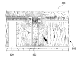
- FIG. 35 is a cross-sectional view showing a configuration example of a conventional mode converter (converter).
- the waveguide 802 in the converter 810, the waveguide 802 has an opening 825 for radiating radio waves on the front end surface (the right side in FIG. 35).
- the waveguide 802 includes a plurality of post (column) walls 820 and ground conductor layers (copper foils) 821 and 822.
- a pin (planar circuit / waveguide converter) 823 is inserted in the waveguide 802 as a power feeding unit.
- the millimeter wave signal introduced from the transmission line 824 to the pin 823 is radiated as an electromagnetic wave from the opening 825 in front of the waveguide 802.
- the converter 810 that is an antenna package is formed by stacking multiple layers via conductors 827A and 827B and a plurality of substrates 828A, 828B, and 828C that are dielectrics.
- the pins 823 are formed by previously forming vias in the substrates 828B and 828C and then stacking the substrates.
- impedance matching is required when connecting circuit A and circuit B. This means that the signal is transmitted without reflection at the connection point from the circuit A to the circuit B. That is, it is necessary to transmit the signal without reflection at the connection point of the planar circuit / transmission line as the circuit A and the waveguide as the circuit B.
- the length of the pin 823 is adjusted to a predetermined value, thereby realizing signal transmission with suppressed reflection loss and impedance matching.
- vias are formed in advance on a plurality of substrates having a predetermined thickness, and the pins are manufactured by laminating these substrates, so the length of the pins depends on the thickness dimension of the substrate.
- the thickness dimension of each substrate to be laminated cannot be determined individually, and depends on whether or not the material is easily available. For this reason, it is difficult to realize a pin having an optimal length.
- the pins in the conventional transducer are configured in the substrate. Therefore, in practice, it is difficult to confirm to which position the pin extends in the substrate. In particular, after the converter is completed, the distance between the pin 823 and the ground conductor layer 822 cannot be adjusted (see Patent Document 2). Also, in the above structure, the designed characteristics cannot be obtained due to the deterioration of the reflection characteristics due to the influence of the conductor or positional deviation when laminating the substrates and the adhesive used when laminating the substrates. It has problems such as becoming larger.
- the conventional converter has a structure in which a plurality of substrates on which vias are formed are stacked. Therefore, unfavorable situations such as an increase in the number of processing steps, an increase in transmission loss due to the adhesive, a variation in transmission characteristics due to the material of each layer, a positional shift in the lamination process, and a difficulty in obtaining the material occur.
- the present invention has been made in consideration of the above points, and provides a mode converter having an optimum pin and capable of easily confirming and adjusting the separation distance between the tip of the pin and the ground conductor layer. Further, the present invention provides a mode converter having a high manufacturing efficiency and having optimum characteristics by reducing processing man-hours.
- 1st aspect of this invention is a mode converter, Comprising: The board
- the end of the pin is exposed on the second main surface of the substrate, and the antipad that electrically insulates the end of the pin from the ground conductor layer is provided on the second main surface. Is provided. Therefore, it is possible to easily confirm the positional relationship between the pin and the ground conductor layer and adjust (trim) the pin and the ground conductor layer.
- the second aspect of the present invention is the mode converter according to the first aspect, wherein the pin extends on the second main surface.
- the mode converter according to the second aspect has a structure in which the interface between the inner wall of the through hole and the pin is not exposed on the second main surface. Accordingly, it is possible to prevent fine particles and the like from entering from the interface.
- a third aspect of the present invention is the mode converter according to the first or second aspect, wherein the pin is formed along the inner wall of the through hole and has a cylindrical shape.
- the mode converter which concerns on a 3rd aspect, when a board
- the antipad has a circular ring shape.
- the difference between the outer diameter and the inner diameter of the antipad having a circular ring shape is 40 to 80 ⁇ m.
- the through hole is filled with a dielectric.
- the difference between the outer diameter and the inner diameter of the antipad having a circular ring shape is 50 to 80 ⁇ m.
- the antipad has a rectangular ring shape.
- the through hole is filled with a dielectric.
- the length between the outer side of the rectangular ring and the inner side of the antipad having the rectangular ring shape is 40 to 120 ⁇ m.
- the end of the pin is exposed at the second main surface, and the antipad for electrically insulating the end of the pin and the ground conductor layer is provided on the second main surface. . Therefore, it is possible to easily confirm the positional relationship between the pin and the ground conductor layer and adjust (trim) the pin and the ground conductor layer.
- the through hole was formed by using drilling, but according to the above aspect of the present invention, the through hole can be formed by a single drilling process. Work reliability and yield can be improved.
- the through holes can be collectively formed in the first substrate and the second substrate, the distance between the through holes of each substrate is smaller than that in the case where the two substrates are individually drilled.
- the position and diameter of the excitation pin are uniformly determined within the substrate, it is possible to reduce deterioration in transmission characteristics.
- the through-hole penetrating from the first main surface to the second main surface is formed in the substrate, it is not necessary to control the height direction of the hole, and the mode converter is easily manufactured. it can.
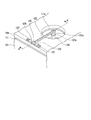
- FIG. 1 is a perspective view schematically showing the configuration of the mode converter 100.
- FIG. 2 is a perspective view schematically showing an enlarged configuration of the transmission path 122 of the mode converter 100.
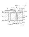
- FIG. 3 is a cross-sectional view taken along the line AA of FIG. 2, schematically showing a configuration example of the mode converter 100. As shown in FIG.
- the mode converter 100 is connected to a substrate 101, a planar circuit (transmission path) 122 for high-frequency signal propagation, and a pin (conductor pin, excitation pin, excitation pin) 120.
- the substrate 101 is a laminated substrate in which a single member or a plurality of base materials are laminated. As shown in FIG. 1, the substrate 101 penetrates from one main surface (first main surface) to the other main surface (second main surface).
- One first through hole (through hole) 103 and a plurality of second through holes 104 are provided.
- the second through-hole 104 is disposed at a position surrounding the first through-hole 103 in a U shape in plan view of the substrate 101.
- the pin 120 has a conductor film 123f and a conductor film 122f on the inner wall (inner wall surface) 103a of the first through hole 103 that penetrates from one main surface 101a to the other main surface 101b of the substrate. They are stacked in order.
- the pin 120 communicates both main surfaces 101 a and 101 b of the substrate via the first through hole 103.
- the conductor film 122f is a film extending from the planar circuit 122.
- the waveguide 110 is erected between the ground conductor layers 111 and 112 and the ground conductor layers 111 and 112 respectively disposed on one main surface 101a and the other main surface 101b of the first substrate (substrate). And a plurality of conductive pillars (posts) 114 connecting the two.
- the conductor pillar 114 is configured by the second through-hole 104 and a conductor disposed therein. Both ends of the conductor pillar 114 are electrically connected to the ground conductor layers 111 and 112, respectively.
- the plurality of conductor pillars 114 are arranged so as to surround the pin 120 in a U shape in a plan view of the first substrate 101.
- the conductive film and the conductive pillar 114 are not disposed on the side of the first substrate 101 on the side of the one end 101c, and an opening 102 through which electromagnetic waves are radiated is formed.
- the conductive pillar 114 confines the electromagnetic wave radiated from the pin 120 in the waveguide 110 when the mode converter 100 is operated. By providing the conductive pillar 114, the radiated electromagnetic wave can be propagated only in a desired direction without leaking.
- the plurality of conductor pillars 114 are arranged in parallel with three sides excluding one side corresponding to the opening 102 in the substantially rectangular peripheral edge in a plan view of the first substrate 101.
- the arrangement of the plurality of conductor pillars 114 reflects the electromagnetic waves radiated from the pins 120 so as not to leak outside. Specifically, when adjacent conductor pillars 114 are spaced apart, the distance L between the central axes of the conductor pillars 114 is smaller than twice the diameter d of the conductor pillars 114 as shown in FIG. Has been determined to be. That is, the interval X between the re-adjacent positions of the conductor pillars 114 is determined to be smaller than the diameter d of the conductor pillars 114.
- the ground conductor layers 111 and 112 are films each made of a conductor such as copper and functioning as an electrically grounded wiring (GND).
- the ground conductor layer 111 is not provided on the peripheral edge portion of the opening 103b of the first through hole in the one main surface 101a of the first substrate.
- the region where the ground conductor layer 111 is not provided and the ground conductor layer 111 and the pin 120 are insulated is the antipad 111a.
- the ground conductor layer 112 is not provided in the peripheral portion of the opening 103c of the first through hole, and there is a region where the ground conductor layer 111 is not provided.
- the anti-pad 112a having a predetermined width H4.
- the anti-pad 111a is defined as an insulating region that extends outward from the opening 103b of the first through hole on one main surface 101a of the first substrate.
- the antipad 112a is defined as an insulating region in which nothing is arranged and extends outward from the opening 103c of the first through hole on the other main surface 101b of the first substrate.
- the region where the antipad 111a and the antipad 112a are formed may be an electrically insulating region, for example, a region where an insulator is provided.
- the conductor layers 111 and 112 and the antipads 111a and 112a may be covered.
- the ground conductor layers 111 and 112 and the antipads 111a and 112a are protected from foreign matters and contamination.
- another substrate can be stacked so as to be in direct contact with the mode converter 100.
- An insulating portion 124 having a substantially uniform thickness is laminated on the conductor film 111, and a transmission path 122 is formed on the outer surface of the insulating portion 124.
- the transmission path 122 is provided so as to overlap at least the antipad 111a.
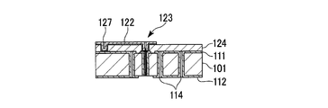
- One end side of the transmission line 122 is connected to the outer end portion of the pin 120 and the other end side is connected to the GSG pad 125 on the insulating portion 124 to form a microstrip line.
- the GND pads 126 are arranged on both sides of the transmission line 122 on the insulating portion 124 so as to be separated from each other on the outer sides of the GSG pad 125.
- a GND connection via 127 is adjacent to both outer sides of the GND pad 126.
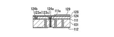
- the GND connection via 127 is formed so as to connect from the insulating portion 124 to the conductor film 111.
- the pin 120 only needs to have at least a surface formed of a conductor such as Cu, Ag, or Au, and the inside can be configured to be occupied by the same conductor, cavity, or insulating resin as the surface. .
- the insulating resin only needs to have an electric conductivity of 0.1 S / m or less as compared with the antipads 111a and 112a.
- the pin 120 is formed along the inner wall 103a of the first through hole, and has a cylindrical shape having an outer diameter H1. Therefore, when the substrate 101 is deformed by applying bending or twisting stress, the pin 120 can also be easily deformed following the deformation, and the mode converter 100 is prevented from being damaged due to excessive stress. be able to.
- the pins 120 are formed perpendicular to both main surfaces (101a, 101b) of the first substrate 101.
- a flange-like land 123 c that is formed in the same layer as the ground conductor layer 111 and is made of the same material as the ground conductor layer 111 is provided around the end of the pin 120 on the one main surface 101 a side of the first substrate 101.
- Outer edge portion 123 d of the surface of land 123 c that is annular in the plan view of first substrate 101 is covered with insulating portion 124.
- the surface of the annular portion 123e on the center side of the land 123c is covered with a conductor 122a that extends from the transmission path 122 and expands in the thickness direction of the insulating portion 124.
- the outer diameter dimension (outer diameter dimension of the land 123c) H3 of the outer edge portion 123d, the outer diameter dimension H2 of the conductor 122a connected to the land 123c, and the outer diameter dimension H1 of the pin 120 are , H3> H2> H1.
- the conductor which comprises the planar circuit 122 mentioned above, the pin 120, the grounding conductor layers 111 and 112, and the conductor pillar 114 consists of titanium (Ti) or chromium (Cr) from the surface side of the 1st board
- a film and a film made of copper (Cu) are sequentially stacked.
- These conductors can be formed using a plating method or a conductive paste.
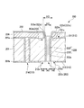
- FIG. 4 is a cross-sectional view of the mode converter 200 taken along the line AA shown in FIG. 2, showing another configuration example of the mode converter 100 shown in FIG. 3 shows an example in which the vicinity of the central axis in the longitudinal direction of the first through hole 103 is a cavity, but as shown in FIG. 4, the conductor 222f in which the inside of the first through hole 203 constitutes the pin 220, It may be filled with 223f.
- the components other than the first through hole 203 are the same as those of the mode converter 100 of FIG.
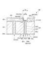
- FIG. 5 is a sectional view of the mode converter 300 taken along the line AA shown in FIG. 2, showing another configuration example of the mode converter 100 shown in FIG.
- a pin 120 is formed along the inner wall 103a of the first through hole, and the exposed surface of the pin 120 exposed on the other main surface 101b side of the first substrate is the other main surface of the first substrate.
- An example is shown in which it is formed on the same surface as the surface 101b.
- the pin 320 may extend from the other main surface 301 b of the first substrate. That is, the pin 320 may have an edge (land) 322b that spreads outward at the opening 303c of the first through hole.
- the interface between the inner wall 303a of the first through hole and the pin 320 is not exposed on the other main surface 301b of the first substrate. Accordingly, it is possible to prevent fine particles and the like from entering from the interface.
- the ground conductor layer disposed on the other main surface of the first substrate functions as a ground terminal (GND). Therefore, the end of the pin on the other main surface of the first substrate is electrically coupled to the ground conductor layer, and the impedance of the pin varies depending on the distance between the end of the pin and the ground conductor layer, that is, the size of the antipad. To do. Accordingly, the impedance of the pin can be controlled to match the impedance of the planar circuit by adjusting the size of the antipad. For example, the operation of the mode converter will be described with reference to FIG. 3.
- the TEM mode is formed between the transmission path 122 forming the microstrip line and the conductor film 111 forming the GND, and the waveguide 110
- the mode of the electric field is converted like the TE mode. 35, since the pin 823 does not penetrate the substrate, an electric field in the thickness direction of the substrate (electric field of the vertical component) is generated between the conductor 827A and the ground conductor layer 822 (FIG. 34). reference). Since this vertical electric field generates an electric field in an oblique direction (indicated by an arrow in FIG. 34) having a vertical component, a TE mode on the front end face (that is, the right side in FIGS. 34 and 35) is induced. . Thereby, the mode conversion of the electric field is performed.
- a through hole 103 and an antipad 112a penetrating the substrate 101 are formed.
- an electric field in a direction perpendicular to the thickness direction of the substrate (electric field of a lateral component) is generated (see FIG. 33).
- an electric field in an oblique direction (indicated by an arrow in FIG. 33) having a vertical component is also generated around the through hole 103 and the antipad 112a.
- the TE mode of the front end face that is, the right side in FIGS. 3 and 33
- the end of the pin is exposed on the other main surface of the first substrate, and the antipad that electrically insulates the end of the pin and the ground conductor layer, It is provided on the other main surface of the substrate. Therefore, the positional relationship between the end portion of the pin and the ground conductor layer can be easily confirmed. Then, by adjusting (trimming) and optimizing while checking the size of the antipad, it is possible to easily realize a transmission line with input impedance matching.
- Adjustment of the size of the antipad is easy as a process, and fine adjustment is possible, so that the input impedance of the planar circuit and the pin can be accurately matched. Therefore, the reflection loss of the signal propagated from the planar circuit to the pin can be accurately controlled by adjusting the size of the antipad. And by optimizing the size of the antipad, the reflection loss can be remarkably reduced.
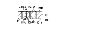
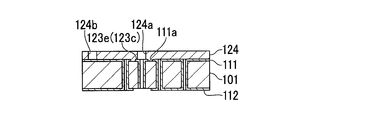
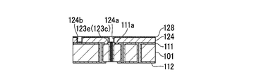
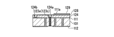
- FIGS. 8A to 8M are cross-sectional views of the main part in each manufacturing process of the mode converter 100 in order of the manufacturing process.
- a first substrate made of glass or the like having transparency that can transmit a laser described later is prepared.
- the thickness of the first substrate is about 850 ⁇ m.
- the modified portion ⁇ and the modified portion ⁇ are formed by irradiating a predetermined position of the first substrate 101 with a laser.
- the reforming portion ⁇ is a region corresponding to a length equal to the thickness of the first substrate 101 from one main surface to the other main surface of the first substrate at a position where the pin inside the first substrate 101 is formed. To form.
- the modified portion ⁇ is formed from one main surface of the first substrate to the other main surface, that is, in a region having a length equal to the thickness of the first substrate 101 at a position where the conductor pillar of the first substrate is formed. To do.
- the reforming part ⁇ has a diameter d and is formed such that the distance X between the reforming part ⁇ and the adjacent reforming part ⁇ is smaller than the diameter d.
- the first substrate 101 may be made of, for example, Pyrex (registered trademark), and forms a modified portion by condensing and irradiating a femtosecond laser having a pulse width of 250 fs as laser light. The dimensions of the modified portions ⁇ and ⁇ are controlled by laser irradiation conditions.
- the laser irradiation method in the first step will be described.
- a portion of the first substrate 101 to be modified is irradiated with the laser beam 12 and the focal point 13 of the laser beam 12 is scanned.
- the modification process proceeds, at least part of the laser beam 12 reaching the focal point 13 does not propagate through the previously formed modified portion, that is, the region modified by the irradiation of the laser beam 12.
- the focal point 13 of the laser beam 12 is scanned.
- the modified portions ⁇ and ⁇ are formed in the first substrate 101 by scanning the focal point 13 of the laser light 12 in the direction of the arrow shown in FIG. 8B.
- the laser beam 12 is preferably irradiated continuously from the surface of the first substrate 101 to the inside, that is, from one main surface side to the other main surface side.
- the modified portion by laser light has a higher refractive index than that of the first substrate 101, but the refractive index distribution in the modified portion and its vicinity is slightly non-uniform, so light propagating through the modified portion. Are randomly reflected and refracted. Therefore, in the first substrate 101, since the laser beam 12 does not propagate through the modified portion before propagating to the condensing portion, the beam diameter is prevented from expanding and the peak intensity is reduced. Can be suppressed. In addition, since at least a part of the laser beam 12 does not propagate through the modified portion 14, it is possible to quickly form a region that is modified by the irradiation of the laser beam 12.
- the modified portion ⁇ and the modified portion ⁇ are removed by etching as a second step. Etching is performed by immersing the glass substrate 101 on which the modified portions ⁇ and ⁇ are formed in a predetermined chemical solution contained in a container (not shown). As a result, the modified portion ⁇ and the modified portion ⁇ are wet-etched with the chemical solution from both sides of the glass substrate 101 and removed from the inside of the glass substrate 101.
- the first through hole 103 and the second through hole 104 are formed in the portion where the reforming portion ⁇ and the reforming portion ⁇ existed.
- an acid solution mainly containing hydrofluoric acid or an acid solution mainly containing potassium hydroxide can be used as the chemical solution.
- the etching in the second step utilizes the phenomenon that the modified part is etched much faster than the unmodified part.
- the fine 1st through-hole 103 and the 2nd through-hole 104 resulting from the shape of the modification parts (alpha) and (beta) can be formed.
- the hole diameters of the fine first through hole 103 and the second through hole 104 can be appropriately determined in the range of 10 ⁇ m to 300 ⁇ m according to the application of the part to be manufactured.
- a seed layer 121a is formed inside one main surface 101a, the first through hole 103, and the second through hole 104 of the first substrate.
- a seed layer 121b is formed on the other main surface 101b of the first substrate.
- Each of the seed layers 121a and 121b can be formed by sputtering, and is made of a mixture of Cr and Cu, a mixture of Ti and Cu, and the like, and preferably has a thickness of about 10 nm to 500 nm.
- a resist by plating is formed around the land formation region connected to the opening 103b of the first through hole on the seed layer 121a.
- 115a is formed.
- a resist 115b is formed by plating around a region overlapping the opening 103c of the first through hole on the seed layer 121b.
- the resist 115a In plan view from the one main surface 101a side of the first substrate, the resist 115a has an annular shape and covers the region corresponding to the antipad 111a excluding the opening 103b and the land 123c portion of the first through hole. Is done. Further, in plan view from the other main surface 101b side of the first substrate, the resist 115b has an annular shape and is formed so as to cover a region corresponding to the antipad 112a excluding the opening 103c of the first through hole.
- the inner diameter dimension H3 of the resist 115a is determined in consideration of the outer diameter dimension H3 of the land 123c.
- a liquid negative resist, a film negative resist, a liquid positive resist, or a film positive resist can be used as the resists 115a and 115b.
- plating layers are grown on the surfaces of the seed layers 121a and 121b excluding the portions covered with the resist 115.
- the plating layer formed on one main surface 101a side of the first substrate is the ground conductor layer 111
- the plating layer formed on the other main surface 101b side is the ground conductor layer 112
- the inside of the first through hole 103 is the plated layer formed on the pin 120 and the plated layer formed inside the second through hole 104.
- the thickness of the plating layer is at least thicker than the skin depth by the millimeter wave band signal. Since the skin depth by a signal of 60 GHz is 270 nm, it is considered to be sufficient to set the thickness to about 2 ⁇ m. Note that the pins 120 and the conductor pillars 114 formed by copper plating may not be completely filled in the first through hole 103 and the second through hole 104, respectively, but airtightness is required. Etc., it is desirable that they are completely filled.
- the resists 115a and 115b are stripped and the remaining seed layers 121a and 112b are etched. Thereby, the conductor film 111, the land 123c, and the antipads 111a and 112a are formed.
- an insulating portion 124 is formed on the conductor film 111 and on the outer periphery of the land 123c.
- the insulating portion 124 includes a portion including the opening portion of the first through hole ⁇ and the annular portion 123e on the center side of the surrounding land 123c, and a portion serving as the GND connection via 127 at the terminal portion of the planar circuit (transmission line) 122. Opened portions 124a and 124b are formed in the overlapping portions.
- the opening around the first through-hole 103 is determined so that the diameter is H2, and as a result, the outer diameter H2 of the portion of the conductor 122a connected to the land 123c is determined as shown in FIG. .
- the insulating portion 124 formed in the fourth step is made of a photosensitive resin, and for example, a liquid material is applied onto the conductive film 111 and the glass substrate surface 111a in the opening portion by spin coating.
- a photosensitive resin layer is cured, the opening 124a around the first through hole 103 and the opening 124b that becomes the GND via 127 are removed by photolithography to form an insulating portion 124. .
- CF 4 gas or O 2 gas is used for the removal.
- RIE Reactive Ion Etching
- the seed layer 128 is formed on the surface of the insulating portion 124, the annular portion 123e of the land 123c, the inside of the hole ⁇ , and the opening as a base forming step that is a pre-step of the transmission path forming step.
- 124b is formed inside.
- the seed layer 128 can be formed by sputtering similarly to the seed layers 121a and 121b, and is made of a mixture of Cr and Cu, a mixture of Ti and Cu, and the like, and preferably has a thickness of about 10 to 500 nm.
- a resist 129 by plating is formed on the seed layer 128 other than the portion where the transmission path 122 is formed.
- the resist 129 is formed so as to cover a region excluding a portion to be the transmission path 122 and a portion for forming a GSG pad (not shown), a GND pad (not shown), and a GND via (not shown).
- the material of the resist 129 may be the same material as the resists 115a and 115b.
- the resist 129 is stripped and the remaining seed layer 128 is etched. As a result, a transmission path 122 forming a microstrip line is formed.
- the mode converter shown in FIGS. 1 to 3 is obtained.
- substrate is limited to members, such as glass which can permeate
- the first through hole and the second through hole can be formed by mechanical processing such as dry etching or drilling. In this case, the members constituting the first substrate are limited. Absent. Further, a passivation film covering the ground conductor layer 112 and the antipad 112a may be formed on the other main surface 101b side of the first substrate.
- the ground conductor layers 111 and 112 and the antipads 111a and 112a are protected from foreign matter adhesion, contamination, and the like.
- another substrate can be stacked so as to be in direct contact with the mode converter 100.
- the passivation film for example, an insulating resin such as polyimide or silicone resin can be used.
- the input impedance of the pin can be adjusted by the size of the antipad provided on the other main surface of the substrate. Therefore, the first through hole provided with the pin only needs to penetrate at least the first substrate, and realize signal transmission with reduced reflection loss without adjusting the length or other circuit elements. Impedance matching can be achieved.
- the antipad is a portion exposed to the outside of the mode converter. Therefore, fine adjustment of the size of the antipad can be performed while visually confirming. The size of the antipad can be readjusted easily even after the mode converter is completed.
- a substrate made of a single base material can be used as the first substrate, not a substrate in which a plurality of base materials are laminated.
- a single base material as the first substrate, it is possible to avoid a number of unfavorable situations such as loss due to adhesive, variation in characteristics of each layer, misalignment in the stacking, etc. when a plurality of base materials are stacked. .
- the diameter of the pin 120 is uniform from the end on the one main surface 101a side of the first substrate to the end on the other main surface 101b side.
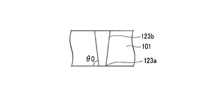
- the end portion 123b on the other main surface 101b side of the first substrate is reduced in diameter than the end portion 123a on the one main surface 101a side, and the side wall surface of the first through-hole 103 is It is also possible to make an angle ⁇ 0 with one main surface 101a of the first substrate. In this case, since the metal adhesion effect inside the first through-hole 103 is improved when film formation is performed from the end 123b side, the seed layer 121a and the copper-plated conductor film 111 can be reliably formed.
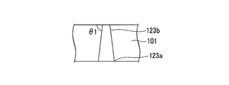
- the first through hole 103 has an end 123 b on the other main surface 101 b side of the first substrate having a diameter larger than that of the end portion 123 a on the one main surface 101 a side.
- the side wall surface of the hole 103 can also form an angle ⁇ 1 with the other main surface 101b of the first substrate.
- the millimeter wave signal at the pin 120 can be smoothly introduced.
- the coupling efficiency to the waveguide can be increased, millimeter wave signals can be introduced smoothly.
- the first through-hole 103 is once reduced in diameter from the end portion 123b on the other main surface 101b side of the first substrate toward the end portion 123a on the one main surface 101a side.
- the angle between the side wall surface of the first through-hole 103 and the other main surface 101b of the first substrate can be increased to ⁇ 3 at the end 123b and ⁇ 4 at the end 123a.
- the metal adhesion effect in the first through hole 103 is improved, so that the seed layer 121a and the copper plating conductor film 111 are reliably formed. can do.
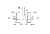
- the end of the transmission line 122 extended from the pin 120 is the GSG pad 125, and the GND connection via 127 is adjacent to the GND pad 126.
- the GND connection via 127 may be on the opposite side of the GSG pad 125 with respect to the GND pad 126.
- the GND connection via 127 b at the pin 120 side position with respect to the GND pad 126 is not limited to the pin 120 side position with respect to the GND pad 126. But you can.
- FIG. 12 is a plan view illustrating a plurality of GND vias having different positions with respect to the GND pad 126 in order to describe the positions of the GND connection vias.
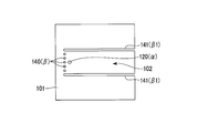
- the waveguide 110 has a plurality of conductor columns 114 as shown in FIG.
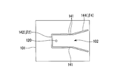
- the side that becomes the rear wall facing the opening 102 is formed with a plurality of conductor pillars 140 and extends in a direction from the pin 120 toward the opening 120.
- the two sides to be used can be slit walls 141 continuous in that direction, and continuous holes can be formed in the first step and the second step.
- the remaining conductor pillars function as the waveguide 110. Can be maintained.
- the side wall of the waveguide 110 is a continuous slit wall 141, leakage of electromagnetic waves can be prevented.
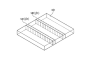
- the side wall of the waveguide 110 is constituted by a plurality of conductor columns that are spaced apart from each other.
- the second through-hole 141 when the second through-hole 141 is formed as described above, as shown in FIG. 14, it can be formed into a shape in which a large number of cylinders are continuously formed so as to overlap in plan view.
- three sides other than the opening 102 in the rectangular waveguide 110 are formed to form a continuous long hole ⁇ 2 to form a U-shaped continuous slit wall 142, and only the vicinity of the opening 102 is separated.
- a waveguide 110 having a conductor post 140 can be formed. In this case, since the environment around the pin 120 is not a post but a sealed space, it is possible to prevent leakage of electromagnetic waves from around the pins when electromagnetic waves are injected.
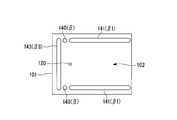
- holes ⁇ 1 and ⁇ 3 that are continuous on three sides of the rectangular waveguide 110 other than the opening 102 are respectively formed to form corresponding slit walls 141 and 143, and portions where the sides intersect.
- a conductor post 140 can be provided to form a state in which the waveguide 110 is separated.
- the discontinuous portion is only one post, disturbance of electromagnetic waves in the discontinuous portion can be minimized, and a mechanically stable structure can be obtained as compared with the structure shown in FIG. It is done.
- the waveguide 110 forms a continuous state on the inner side and the outer side, so that the first substrate 101 is not separated.
- a slit wall 144 having a form in which the distance between the opposing conductor pillars 114 is increased can be provided outside the opening 102.
- an H-plane fan type horn antenna can be formed, and the antenna gain can be improved.
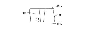
- the diameter of the conductor pillar 114 is determined to be uniform from one main surface 101a of the first substrate 101 to the other main surface 101b.
- the diameter can be reduced from the main surface 101a toward the main surface 101b so as to have an angle ⁇ 5.
- the metal adhesion effect inside the hole ⁇ can be improved, and the seed layer 121a and the copper-plated conductor column can be reliably formed.
- the angle ⁇ 5 the metal adhesion effect inside the hole ⁇ can be improved, and the seed layer 121a and the copper plating conductor film 111 can be reliably formed.
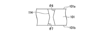
- the conductor pillar 114 can be formed so as to have a diameter of once reduced from the front surface 101a toward the back surface 101b so as to have an angle ⁇ 6 and an angle ⁇ 7.
- the angles ⁇ 6 and ⁇ 7 the metal adhesion effect inside the first through hole 103 can be improved, and the seed layer 121a and the copper-plated conductor film 111 can be reliably formed.
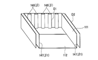
- the conductor films D1 and D2 can be formed only on the surface of the conductor pillar 146 and only on the surface of the slit wall 147. That is, the conductor is not filled in the corresponding hole ⁇ and long hole ⁇ 1 by plating, and may be hollow. In these cases, the conductor films 111 and 112 can be provided only in the corresponding portions between the inner surfaces of the slit walls 147 facing each other. In this case, it is preferable that both ends of the conductor column 146 are securely connected to the conductor films 111 and 112.
- a part of the conductor pillar 114 having a gap has a structure having the slit walls 141, 142, 143, 144, and 147, so that the conductor films 111 and 112 forming the waveguide 100 are formed.
- Most of the waveguide 110 between them can be replaced with slit walls 141, 142, 143, 144, 147.
- the leakage of electromagnetic waves can be significantly suppressed as compared with the conventional case, the radiation efficiency of the antenna can be improved, and the radiation loss of the waveguide can be reduced.
- the slit wall the area through which the current flows becomes larger than the case where only the conductor pillar 114 is used. Accordingly, it is possible to greatly reduce the transmission mode disturbance and failure due to electrical non-conduction between the post wall 114 and the conductor films 111 and 112, which may occur in the case of all the post walls 114, and the risk thereof.
- FIG. 21 is a cross-sectional view of the mode conversion module 500.
- a mode conversion module 500 includes a wireless communication IC (semiconductor chip) 510 having a wireless transmission / reception functional element on a side where the planar circuit 122 of the mode converter 100 of this embodiment is disposed. Connected and configured.
- IC semiconductor chip
- a conductor film 111 for forming GND and a transmission path 122 on the insulating portion 124 are provided, and at the same level as these layers.
- a circuit (not shown) is provided.
- a transmission line termination unit 125 functioning as a GSG pad is connected to a terminal 511 of the wireless communication IC 510. Since a high-frequency signal such as a millimeter wave is greatly affected by parasitic inductance, it is desirable that the connection between the terminal portion 125 and the terminal 511 is performed by a short distance mounting using a bump rather than a wire bond. Note that the electromagnetic field of the electromagnetic wave guiding portion is shielded from the external environment by the post and the continuous wall, and thus is not affected by the external environment such as the mounting environment.
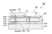
- FIG. 22 is a cross-sectional view of the mode conversion unit 600 in which the mode conversion module 550 is mounted on the second substrate (mother substrate, motherboard) 513.
- the mode conversion module 550 has a third through hole 605 that penetrates the mode converter 100 in the thickness direction.
- the wireless communication IC 510 and the second substrate 513 are electrically connected by the third through hole 605.
- An underfill material (not shown) may be filled between the mode conversion module 550 and the second substrate 513.
- the ground conductor layer and the antipad of the mode converter 100 may be covered with the underfill material, and the first substrate 101 and the second substrate 513 may be bonded.
- the components other than the third through hole 605 are the same as those of the mode conversion module 500 of FIG.
- FIG. 23 is a cross-sectional view of the mode conversion unit 700 in which a mode conversion module 560 having a configuration different from that of the mode conversion module 500 of FIG. 21 is mounted on a second substrate (mother substrate, motherboard) 513.
- the mode conversion module 560 includes a semiconductor chip 510, and a conductor film 713b disposed on the surface of the mode converter 100 and a terminal (not shown) of the semiconductor chip 510 are electrically connected via a wire 512. Yes.
- the mode conversion module 560 has a third through hole 705 that penetrates the mode converter 100 in the thickness direction.
- the wireless communication IC 510 and the second substrate 513 are electrically connected by the third through hole 705.
- An underfill material (not shown) may be filled between the mode conversion module 560 and the second substrate 513.
- the ground conductor layer and the antipad of the mode converter 100 may be covered with the underfill material, and the first substrate 101 and the second substrate 513 may be bonded.
- Components other than the wireless communication IC 510 and the third through hole 705 are the same as those of the mode conversion module 500 of FIG.
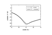
- Example 1 A first embodiment using the above-described mode converter will be described. Of the signals propagated from the planar circuit (high-frequency transmission path) to the pin, the reflection is performed when the mode converter according to the present embodiment (FIG. 5) is used and when the mode converter according to the conventional technique (FIG. 35) is used. The simulation about the component (reflection loss) to perform was performed. Three-dimensional electromagnetic field analysis software HFSS was used for the simulation, and the thickness of the first substrate was set to 850 ⁇ m in both the present embodiment and the conventional technology. The result of the simulation is shown in the graph of FIG. In the mode converter of the present embodiment, the size of the other antipad on the first substrate is 100 ⁇ m.
- the horizontal axis of the graph represents the frequency of the signal propagated from the transmission circuit to the pin, and the vertical axis represents the reflection loss S11 at the pin of the propagated signal.
- the solid line on the graph corresponds to the result by the mode converter of the present embodiment, and the broken line corresponds to the result by the mode converter of the prior art.
- the two lines since the two lines almost coincide, it was found that the same frequency dependence of the reflection loss can be obtained in any of the mode converters of the present embodiment and the prior art. .
- a pin is formed so as to penetrate the first substrate as in the present embodiment, and the size of the antipad is adjusted so that the length of the pin itself is adjusted as in the prior art. It was found that impedance matching at the level can be realized.
- Example 2 A second embodiment using the above-described mode converter will be described.
- the other main signal of the first substrate in the case of using the mode converter (FIG. 5) according to the present embodiment and the case of using the mode converter (FIG. 35) of the prior art.
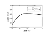
- a simulation was performed on a component (transmission loss) leaking from the opening on the surface 301b side.
- Three-dimensional electromagnetic field analysis software HFSS was used for the simulation, and the thickness of the first substrate was set to 850 ⁇ m in both the present embodiment and the conventional technology. The result of the simulation is shown in the graph of FIG.
- the size of the other antipad on the first substrate is 100 ⁇ m.
- the horizontal axis of the graph indicates the frequency of the signal propagated from the transmission circuit to the pin, and the vertical axis indicates the transmission loss S21 from the pin of the propagated signal.
- the solid line on the graph corresponds to the result by the mode converter of the present embodiment, and the broken line corresponds to the result by the mode converter of the prior art. As shown in the graph, since the two lines are almost coincident, it has been found that the same frequency dependence of transmission loss can be obtained in any of the mode converters of the present embodiment and the prior art. .
- Example 3 A third embodiment using the above-described mode converter will be described.
- the mode converter according to the present embodiment is used (FIG. 5) and when the mode converter according to the conventional technique (FIG. 35) is used, it is generated inside the first substrate.
- a simulation was performed on the distribution of the electric field.
- Three-dimensional electromagnetic field analysis software HFSS was used for the simulation, and the thickness of the first substrate was set to 850 ⁇ m in both the present embodiment and the conventional technology.
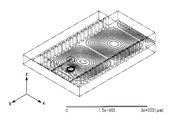
- the simulation result by a prior art and the simulation result by this embodiment are shown to FIG. 26A and FIG. 26B, respectively.
- the electric field distribution actually varies with time, and these are graphs showing the electric field distribution at a certain moment.
- the size of the antipad 312a is 100 ⁇ m.
- the direction from the pin opening 303b toward the GSG pad 125 shown in FIG. 2 is the y-axis, and the direction that is 90 degrees with the y-axis in the plane parallel to both main surfaces 301a and 301b of the first substrate is the first axis.
- the direction from the other main surface 301b of the substrate toward the one main surface 301a was taken as the z-axis.
- the strongest portion of the electric field exists in the vicinity of the pin, and a distribution in which the electric field becomes weaker in inverse proportion to the distance from the strongest portion was observed.
- the portions where the electric field is strong are periodically arranged at regular intervals in the ( ⁇ y) direction away from the pin 120, and a similar distribution is observed in each portion.
- FIG. 26A and FIG. 26B comparing the simulation results at positions equidistant from the pin, it was found that the electric field distributions of both were almost the same.
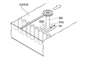
- Example 4 A fourth embodiment using the above-described mode converter will be described.
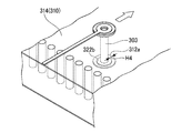
- the antipad 312a has a circular ring shape, and has a size different by 10 ⁇ m in a range where the difference H4 between the outer diameter and the inner diameter is 30 ⁇ m or more and less than 90 ⁇ m.
- FIG. 27 schematically shows the shape of the antipad 312a.
- a circular ring-shaped land 322b for controlling the capacitance value of the antipad is also formed at the tip of the pin.
- H4 is a difference between the outer diameter of the land 322b and the outer diameter of the antipad 312a.
- the outer diameter of the land 322b is larger than the outer diameter of the pin 320, and the center of the land 322b is arranged so as to coincide with the center of the pin.
- an electric field in a direction perpendicular to the thickness direction of the substrate 301 is generated from the outer peripheral surface of the land 322b to the ground conductor layer 312.
- the direction in which the TE mode electromagnetic wave travels is indicated by an arrow.
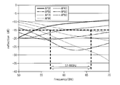
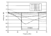
- Three-dimensional electromagnetic field analysis software HFSS was used for the simulation, and the thickness of the first substrate was set to 850 ⁇ m in both the present embodiment and the conventional technology. Moreover, the inside of the first through hole 303 was filled with resin, and the resin was simulated as a dielectric having a relative dielectric constant of 3.4. The results are shown in the graph of FIG.
- the horizontal axis of the graph represents the frequency of the signal propagated from the transmission circuit to the pin, and the vertical axis represents the reflection loss S11 at the pin of the propagated signal.
- the reflection loss S11 sufficient as a mode converter is set to about ⁇ 15 dB or less, and ⁇ 15 dB is set as a threshold value.
- the use frequency band is about 57 to 66 GHz.
- the size of the antipad (that is, H4) is preferably 50 ⁇ m or more and less than 80 ⁇ m.
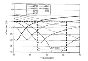
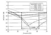
- Example 5 A simulation was performed under the same experimental conditions using the same mode converter as in Example 4 except that the inside of the first through hole 303 was not filled with a dielectric. The result of the simulation is shown in the graph of FIG.
- the size of the antipad (that is, H4) is preferably 40 ⁇ m or more and less than 80 ⁇ m.
- Example 6 A simulation similar to that of Example 4 was performed using the rectangular ring-shaped antipad 312a. The same mode converter as in Example 4 was used, and the experimental conditions were also the same.
- FIG. 30 schematically shows the shape of the antipad.
- the rectangular ring-shaped antipad 312a used in the simulation was set to 40, 50, 60, 80, and 120 ⁇ m in the range where the width H4 shown in FIG. 5 is 40 ⁇ m or more and less than 120 ⁇ m.
- a rectangular ring-shaped land 322 b for controlling the capacitance value by the antipad is also formed at the tip of the pin 320.
- H4 is a distance between one side of the land 322b and one side of the ground conductor layer 312 facing each other across the insulating region.
- the length from the center of the land 322b to the outer frame is larger than the outer diameter of the pin 320, and the center of the land 322b is arranged to coincide with the center of the pin 320.
- an electric field having a direction that includes many components in the direction perpendicular to the thickness direction of the substrate (lateral component) is generated, so that the TE mode can be induced more efficiently.
- the direction in which the TE mode electromagnetic wave travels is indicated by an arrow.
- one side of the land 322b and one side of the outer frame of the rectangular antipad 312a are parallel to each other with an interval of H4, and the TE mode electromagnetic wave indicated by the arrow advances. It is preferable to be arranged so as to be perpendicular to the direction.
- the result of the simulation is shown in the graph of FIG. From the results shown in the graph, it was found that even when a rectangular ring-shaped antipad was used, the magnitude of reflection loss varied with the size of the antipad. In all the ranges where H4 is 40 to 120 ⁇ m, the reflection loss below the threshold value was shown in the above-mentioned use frequency band. Therefore, the size of the antipad is preferably 40 to 120 ⁇ m. As a result, it has been found that it is possible to control the reflection loss at the pin, that is, to control the impedance at the pin to match the impedance of the planar circuit.
- Example 7 A simulation was performed under the same experimental conditions using the same mode converter as in Example 6 except that the inside of the first through hole 203 was not filled with a dielectric. The result of the simulation is shown in the graph of FIG.
- the size of the antipad is preferably 40 to 120 ⁇ m.
- the present invention can be widely applied as a device for high-speed and large-capacity communication of several Gbps using the millimeter wave band.
Landscapes
- Production Of Multi-Layered Print Wiring Board (AREA)
- Waveguides (AREA)
- Structure Of Printed Boards (AREA)
- Internal Circuitry In Semiconductor Integrated Circuit Devices (AREA)
Abstract
モード変換器は、第一主面および第二主面を有する基板と、第一主面に形成された第一接地導体層と、第二主面に形成された第二接地導体層と、第一主面に形成された、高周波を伝播する平面回路と、平面回路と接続され、第一主面から第二主面まで貫通する貫通孔の内部に形成され、第一主面および第二主面に連通するピンと、第二主面において露出したピンの端部と、第二接地導体層との間に形成されたアンチパッドと、を備える。
Description
本発明は、モード変換器に係り、特にミリ波帯の通信用の導波路に用いられる技術に関する。
本願は、2012年12月27日に出願された特願2012-283993号に基づき優先権を主張し、その内容をここに援用する。
本願は、2012年12月27日に出願された特願2012-283993号に基づき優先権を主張し、その内容をここに援用する。
近年、ミリ波帯を利用した数G[bps]の高速大容量通信が提案され、その一部が実現されつつある。特に、60GHz帯で動作する無線通信機器は、より重要性を増している。57~66GHzまでの広い周波数帯域を、無免許で利用可能であることから、民生分野への普及が期待されており、安価で小型のミリ波通信モジュールの実現が急務である。
小型で安価なミリ波通信モジュールを実現する形態として、非特許文献1、特許文献1には、プリント基板による導波路(ポスト壁導波路アンテナ:PWA Post-wall Waveguide Antenna)を利用したミリ波モジュールが開示されている。特許文献1の図1~図7に示すように、上記技術では、従来の導波路の側壁(金属壁)を、プリント基板の貫通孔群(ポスト群)で置き換えている。無線通信IC(CMOS-IC)がPWAの上に実装されており、ワイヤボンド、バンプ接続等の方法で無線通信IC(特許文献1の明細書中では半導体チップ4と表記。以下同)から出力されたミリ波信号は、一旦、平面回路による伝送線路(マイクロストリップ、コプレーナ、ストリップ等の線路24と表記)を伝わり、平面回路・導波路変換構造(中心導体23と表記)を経て、最終的には導波路構造部(導波路2と表記)へと導かれる。
図35は従来のモード変換器(変換器)の構成例を示す断面図である。図35に示すように、変換器810において、導波路802は、前方端面(図35の右方側)に、電波を放射する開口部825を有する。導波路802は複数のポスト(柱)壁820と接地導体層(銅箔)821、822とにより構成されている。導波路802には、給電部としてピン(平面回路・導波路変換器)823が挿入されている。伝送線路824からピン823へ導入されたミリ波信号は、導波路802の前方の開口部825から電磁波として放射される。アンテナパッケージである変換器810は、導体827A、827B、および、誘電体である複数の基板828A、828B、828Cを介して多層に積層して形成される。ピン823は、基板828Bと828Cとに予めビアを形成し、そのあとに基板を積層することで形成されている。
一般的な高周波回路においては、回路Aと回路Bとを接続する場合にインピーダンス整合が取られていることが必要である。これは、回路Aから回路Bの接続点において信号を反射なく伝送させることを意味している。つまり、回路Aとしての平面回路・伝送線路から回路Bとしての導波路の接続点において、信号が反射することなく伝送させることが必要である。図35に示すような構造の場合、所定の周波数帯域において、ピン823の長さを所定の値に調整することによって、反射損を抑制した信号伝送を実現してインピーダンス整合が取られている。その他にも、インピーダンス整合方法の一つとして、ピン823と接地導体層822との距離を最適化する方法もある。
R. Suga,et al. "Cost-Effective 60-GHz Antenna-Package with End-Fire Radiation from Open-Ended Post-Wall Waveguide for Wireless File-Transfer System",2011 IEEE MTT-S International Microwave Symposium, pp. 348-351
従来の変換器の製造方法では、厚みの決まった複数の基板に予めビアを形成し、これらの複数の基板を積層させてピンを製造するため、ピンの長さは基板の厚さ寸法に依存して離散的な値しか取ることができず、インピーダンス調整が容易ではない。また、積層する各々の基板の厚さ寸法が、個別に決定可能ではなく、材料が入手し易いか否か等に依存する。そのため、最適な長さのピンを実現しにくい。
また、従来の変換器におけるピンは基板内に構成されている。そのため、実際には、ピンが基板内のどの位置まで延びているかを確認することが難しい。特に、変換器が完成した後では、ピン823と接地導体層822との距離を調整(特許文献2参照)できない。
また、上記構造では、基板積層時の導体または位置ずれおよび基板積層時に用いる接着材の影響により、反射特性が劣化する等して設計通りの特性が得られず、引いては導波路の損失が大きくなる等の問題を有する。
また、上記構造では、基板積層時の導体または位置ずれおよび基板積層時に用いる接着材の影響により、反射特性が劣化する等して設計通りの特性が得られず、引いては導波路の損失が大きくなる等の問題を有する。
さらに、従来の変換器は、ビアが形成された基板を複数積層させた構造を有する。そのため、加工工数の増加、接着材による伝送損失の増加、各層の材料に起因した伝送特性ばらつき、積層工程における位置ズレ、材料が入手しにくい等の好ましくない状況が発生する。
本発明は以上のような点を考慮してなされたものであり、最適なピンを有し、ピンの先端と接地導体層との離間距離の確認および調整が容易なモード変換器を提供する。また、加工工数を低減して、最適な特性を有する製造効率の高いモード変換器を提供する。
本発明の第1態様は、モード変換器であって、第一主面および第二主面を有する基板と、第一主面に形成された第一接地導体層と、第二主面に形成された第二接地導体層と、第一主面に形成された、高周波を伝播する平面回路と、平面回路と接続され、第一主面から第二主面まで貫通する貫通孔の内部に形成され、第一主面および第二主面に連通するピンと、第二主面において露出したピンの端部と、第二接地導体層との間に形成されたアンチパッドと、を備える。
第1態様に係るモード変換器によれば、ピンの端部が基板の第二主面において露出しており、ピンの端部と接地導体層とを電気絶縁させるアンチパッドが、第二主面に設けられている。そのため、ピンと接地導体層との位置関係の確認およびピンと接地導体層との調整(トリミング)を容易に行うことができる。
本発明の第2態様は、第1態様に係るモード変換器において、ピンは、第二主面上に延設されている。
第2態様に係るモード変換器によれば、第二主面において、貫通孔の内壁とピンとの界面が露出しない構造となる。したがって、界面から微粒子等が侵入することを防ぐことができる。
本発明の第3態様は、第1または第2態様に係るモード変換器において、ピンは、貫通孔の内壁に沿って形成され、円筒形を有する。
第3態様に係るモード変換器によれば、ピンは円筒形であり、曲げまたは捻じれの応力が加わることによって基板が変形した場合に、ピンも追従して容易に変形可能である。したがって、過剰な応力が加わってモード変換器が破損することを防ぐことができる。
本発明の第4態様は、第1~第3態様に係るモード変換器において、アンチパッドは、円形リング形状を有する。
本発明の第5態様は、第4態様に係るモード変換器において、円形リング形状を有するアンチパッドの、外径と内径との差が、40~80μmである。
本発明の第6態様は、第4態様に係るモード変換器において、貫通孔には、誘電体が充填されている。
本発明の第7態様は、第6態様に係るモード変換器において、円形リング形状を有するアンチパッドの、外径と内径との差が、50~80μmである。
本発明の第8態様は、第1~第3態様に係るモード変換器において、アンチパッドは、矩形リング形状を有する。
本発明の第9態様は、第8態様に係るモード変換器において、貫通孔には、誘電体が充填されている。
本発明の第10態様は、第8または第9態様に係るモード変換器において、矩形リング形状を有するアンチパッドの、矩形リングの外側の一辺と内側の一辺との間の長さが、40~120μmである。
上記第4~第10態様に係るアンチパッドの形状を有するモード変換器によれば、ピンにおける反射損失の制御、すなわちピンにおけるインピーダンスを平面回路のインピーダンスと整合させる制御が可能である。
本発明の第4態様は、第1~第3態様に係るモード変換器において、アンチパッドは、円形リング形状を有する。
本発明の第5態様は、第4態様に係るモード変換器において、円形リング形状を有するアンチパッドの、外径と内径との差が、40~80μmである。
本発明の第6態様は、第4態様に係るモード変換器において、貫通孔には、誘電体が充填されている。
本発明の第7態様は、第6態様に係るモード変換器において、円形リング形状を有するアンチパッドの、外径と内径との差が、50~80μmである。
本発明の第8態様は、第1~第3態様に係るモード変換器において、アンチパッドは、矩形リング形状を有する。
本発明の第9態様は、第8態様に係るモード変換器において、貫通孔には、誘電体が充填されている。
本発明の第10態様は、第8または第9態様に係るモード変換器において、矩形リング形状を有するアンチパッドの、矩形リングの外側の一辺と内側の一辺との間の長さが、40~120μmである。
上記第4~第10態様に係るアンチパッドの形状を有するモード変換器によれば、ピンにおける反射損失の制御、すなわちピンにおけるインピーダンスを平面回路のインピーダンスと整合させる制御が可能である。
上記本発明の態様によれば、ピンの端部が第二主面において露出しており、ピンの端部と接地導体層とを電気絶縁させるアンチパッドが、第二主面に設けられている。そのため、ピンと接地導体層との位置関係の確認およびピンと接地導体層との調整(トリミング)を容易に行うことができる。
また、従来ではドリル加工を用いて貫通孔を形成していたが、上記本発明の態様によれば、一回の孔開けプロセスにより貫通孔を形成することができるため、作業工程の効率化し、作業の信頼性および歩留まりを向上させることができる。
上記本発明の態様によれば、第一基板および第二基板に一括して貫通孔を形成できるため、2つの基板に個別に孔開け作業を行う場合と比較して、各基板の貫通孔間の位置合せが不要になる。そのため、貫通孔間の位置ずれが無くなり、位置ずれに起因した伝送特性の劣化を低減できる。また、ピンの端部と接地導体層との位置関係を容易に確認できる。
また、従来ではドリル加工を用いて貫通孔を形成していたが、上記本発明の態様によれば、一回の孔開けプロセスにより貫通孔を形成することができるため、作業工程の効率化し、作業の信頼性および歩留まりを向上させることができる。
上記本発明の態様によれば、第一基板および第二基板に一括して貫通孔を形成できるため、2つの基板に個別に孔開け作業を行う場合と比較して、各基板の貫通孔間の位置合せが不要になる。そのため、貫通孔間の位置ずれが無くなり、位置ずれに起因した伝送特性の劣化を低減できる。また、ピンの端部と接地導体層との位置関係を容易に確認できる。
上記本発明の態様によれば、励振ピンの位置および径が、基板内で画一的に定められるため、伝送特性の劣化を低減できる。
上記本発明の態様によれば、基板に、第一主面から第二主面まで貫通する貫通孔が形成されるので、孔の高さ方向の制御も不要となり、モード変換器を容易に製造できる。
上記本発明の態様によれば、基板に、第一主面から第二主面まで貫通する貫通孔が形成されるので、孔の高さ方向の制御も不要となり、モード変換器を容易に製造できる。
以下、好適な実施形態に基づき、図面を参照して本発明を説明する。なお、以下に示す実施形態は、発明の趣旨をより良く理解させるために、例を挙げて説明するものであり、特に指定のない限り、本発明を限定するものではない。また、以下の説明に用いる図面は、本発明の特徴を分かりやすくするために、便宜上、要部となる部分を拡大している場合があり、各構成要素の寸法比率等が実際と同じであるとは限らない。
モード変換器の構成
本発明の一実施形態に係るモード変換器100の構成について、図1~3を用いて説明する。図1は、モード変換器100の構成を模式的に示す斜視図である。図2は、モード変換器100の伝送路122の構成を拡大して模式的に示す斜視図である。図3は、モード変換器100の構成例を模式的に示す、図2のA-Aラインに沿った断面図である。
本発明の一実施形態に係るモード変換器100の構成について、図1~3を用いて説明する。図1は、モード変換器100の構成を模式的に示す斜視図である。図2は、モード変換器100の伝送路122の構成を拡大して模式的に示す斜視図である。図3は、モード変換器100の構成例を模式的に示す、図2のA-Aラインに沿った断面図である。
図1~3に示すように、モード変換器100は、基板101と、高周波信号伝播用の平面回路(伝送路)122と、ピン(導体ピン、励起ピン、励振ピン)120と、グランド接続された接地導体層(導体膜)111と、接地導体層(導体膜)112と、導波路110とを備えている。
基板101は単一の部材または複数の基材を積層した積層基板であり、図1に示すように、一方の主面(第一主面)から他方の主面(第二主面)まで貫通する、一つの第一貫通孔(貫通孔)103および複数の第二貫通孔104を有している。第二貫通孔104は、基板101の平面視において第一貫通孔103をU字形に囲む位置に配されている。
ピン120は、図3に示すように、基板の一方の主面101aから他方の主面101bまで貫通する第一貫通孔103の内壁(内壁面)103aに、導体膜123f、導体膜122fが、順に積層されて構成されている。ピン120は、第一貫通孔103を経由して、基板の両方の主面101a、101bを連通している。導体膜122fは、平面回路122から延設された膜である。
導波路110は、第一基板(基板)の一方の主面101a、他方の主面101bにそれぞれ配された接地導体層111、112と、接地導体層111、112の間に立設し、両者を連結する複数の導体柱(ポスト)114とからなる。導体柱114は、第二貫通孔104とその内部に配された導体とによって構成されている。導体柱114の両端はそれぞれ接地導体層111、112に電気的に接続されている。
図1に示すように、複数の導体柱114は、第一基板101の平面視においてピン120をU字形に囲むように配されている。また、第一基板101の側面における一端101c側には、導体膜および導体柱114は配されておらず、電磁波が放射される開口部102が形成されている。導体柱114は、モード変換器100を動作させた際に、ピン120から放射された電磁波を、導波路110内に閉じ込める。導体柱114を備えることにより、放射された電磁波を漏洩させることなく、所望の方向にのみ伝播させることができる。
複数の導体柱114は、第一基板101の平面視において、略矩形をなす周縁部のうち、開口部102に対応する一辺を除いた三辺と平行に配列されている。複数の導体柱114の配列は、ピン120から放射される電磁波を反射して外部に漏洩しないようにされている。具体的には、隣り合う導体柱114が離間して配置された場合、導体柱114の中心軸間距離Lは、図7に示すように、導体柱114の直径dの2倍よりも小さくなるように決定されている。つまり、導体柱114の再近接位置どうしの間隔Xは、導体柱114の直径dよりも小さくなるように決定されている。
接地導体層111、112は、それぞれ銅等の導体によって構成され、電気的に接地された配線(GND)として機能する膜である。接地導体層111は、第一基板の一方の主面101aにおける第一貫通孔の開口部103bの周縁部には設けられていない。接地導体層111が設けられておらず、接地導体層111とピン120とを絶縁する領域が、アンチパッド111aである。第一基板の他方の主面101bにおいても同様に、接地導体層112は、第一貫通孔の開口部103cの周縁部には設けられておらず、接地導体層111が設けられていない領域が、所定の幅H4のアンチパッド112aである。
なお、アンチパッド111aは、第一基板の一方の主面101aにおいて、第一貫通孔の開口部103bから外側に広がる、絶縁領域として定義される。そして、アンチパッド112aは、第一基板の他方の主面101bにおいて、第一貫通孔の開口部103cから外側に広がる、何も配されていない絶縁領域として定義される。なお、アンチパッド111a、アンチパッド112aが形成される領域は、電気的な絶縁領域であればよく、例えば絶縁体が配された領域であってもよい。例えば、第一基板の一方の主面101a側に形成された絶縁部124、または、第一基板の他方の主面101b側に形成された絶縁部(図示せず、パッシベーションとも言う)によって、接地導体層111、112、および、アンチパッド111a、112aが被覆されていてもよい。絶縁部が形成されていることにより、接地導体層111、112、および、アンチパッド111a、112aが異物付着や汚染等から保護される。また、モード変換器100に対して直に接するように、他の基板を積層することができる。
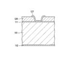
導体膜111には略均一な厚さの絶縁部124が積層され、絶縁部124の外側表面上に伝送路122が形成されている。伝送路122は、少なくともアンチパッド111aと重なるように設けられている。伝送路122は、一端側がピン120の外部側端部に接続され、他端側が絶縁部124上のGSGパッド125に接続されて、マイクロストリップラインを形成している。
GSGパッド125の両外側には、図2に示すように、絶縁部124上の伝送路122の両側に、GNDパッド126が離間して配置される。GNDパッド126の両外側には、図2に示すように、GND接続ビア127が隣接される。GND接続ビア127は、図6に示すように、絶縁部124上から、導体膜111までを接続するように形成される。
ピン120は、少なくとも表面がCu、Ag、Au等の導体から形成されていればよく、内部については、表面と同様の導体、空洞、あるいは、絶縁樹脂等で占有された構造とすることができる。絶縁樹脂は、アンチパッド111a、112aと比して0.1S/m以下の電気伝導率を有していればよい。
ピン120は、図3に示すように、第一貫通孔の内壁103aに沿って形成されており、外径H1を有する円筒状である。したがって、曲げまたは捻じれの応力が加わることによって基板101が変形した場合に、ピン120も追従して容易に変形することができ、過剰な応力が加わってモード変換器100が破損することを防ぐことができる。
ピン120は、第一基板101の両方の主面(101a、101b)に対して垂直に形成されている。第一基板101の一方の主面101a側におけるピン120の端部に、接地導体層111と同階層をなし、接地導体層111と同一材料からなるフランジ状のランド123cが周設される。第一基板101の平面視において円環状とされるランド123cの表面のうち外縁部123dは、絶縁部124によって覆われている。ランド123cの中央側の円環部123eの表面は、伝送路122から延長されるとともに絶縁部124の厚さ方向に拡径する導体122aによって覆われている。
図3に示すように、外縁部123dの外径寸法(ランド123cの外径寸法)H3、ランド123cに接続される部分の導体122aの外径寸法H2、および、ピン120の外径寸法H1は、H3>H2>H1となるように決定される。
なお、上述した平面回路122、ピン120、接地導体層111、112、導体柱114を構成する導体は、第一基板101または樹脂124の表面側から、チタン(Ti)またはクロム(Cr)からなる膜、銅(Cu)からなる膜を、順に積層して形成される。これらの導体は、めっき法または導電性ペーストを用いて形成することができる。
図4は、図3のモード変換器100に対する他の構成例を示す、モード変換器200の、図2で示すA-Aラインに沿った断面図である。図3においては、第一貫通孔103の長手方向の中心軸近傍が空洞である例を示したが、図4に示すように、第一貫通孔203の内部がピン220を構成する導体222f、223fによって充填されていてもよい。第一貫通孔203以外の構成要素は、図3のモード変換器100と同様である。
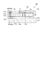
図5は、図3のモード変換器100に対する他の構成例を示す、モード変換器300の、図2で示すA-Aラインに沿った断面図である。図3においては、第一貫通孔の内壁103aに沿ってピン120が形成されており、第一基板の他方の主面101b側に露出したピン120の露出面が、第一基板の他方の主面101bと同一面上に形成されている例を示した。しかし、図5に示すように、ピン320は、第一基板の他方の主面301bよりも延設されていてもよい。すなわち、ピン320は、第一貫通孔の開口部303cにおいて外側に広がる縁部(ランド)322bを有していてもよい。
上記構成にすることにより、第一基板の他方の主面301bにおいて、第一貫通孔の内壁303aとピン320との界面が露出しない。したがって、界面から微粒子等が侵入することを防ぐことができる。
以上説明したように、本実施形態に係るモード変換器によれば、第一基板の他方の主面に配された接地導体層がグランド端子(GND)として機能する。そのため、第一基板の他方の主面においてピンの端部が、接地導体層と電界結合し、ピンのインピーダンスは、ピンの端部と接地導体層との離間距離、すなわちアンチパッドのサイズによって変化する。したがって、アンチパッドのサイズを調整することによってピンのインピーダンスを、平面回路のインピーダンスと整合するように制御することができる。
なお、例えば図3を用いてモード変換器の動作を説明すると、モード変換器では、マイクロストリップラインを形成する伝送路122とGNDを形成する導体膜111との間はTEMモード、導波路110内を伝搬するのはTEモードのように、電界のモードが変換される。
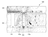
図35の従来例の構成では、ピン823が基板を貫通していないため、導体827Aと接地導体層822との間で基板の厚み方向の電界(縦向き成分の電界)が発生する(図34参照)。この垂直な電界が、縦向き成分を有する斜め方向(図34において矢印で示す)の電界を発生させるため、前方端面(すなわち、図34、図35の右方側)のTEモードが誘起される。これにより、電界のモード変換が行われている。
一方、本願の構成では、例えば図3に示すように、基板101を貫通する貫通孔103とアンチパッド112aとが形成されている。アンチパッド112aでは、基板の厚み方向に対して垂直な方向の電界(横向き成分の電界)が発生する(図33参照)。しかし、貫通孔103周辺およびアンチパッド112a周辺では、縦向き成分を有する斜め方向(図33において矢印で示す)の電界も発生する。この縦向き成分を有する斜め方向の電界により、前方端面(すなわち、図3、図33の右方側)のTEモードが誘起される。従って、本願のように、貫通孔103とアンチパッド112aとを備える構成であっても、モード変換器として動作可能である。
なお、例えば図3を用いてモード変換器の動作を説明すると、モード変換器では、マイクロストリップラインを形成する伝送路122とGNDを形成する導体膜111との間はTEMモード、導波路110内を伝搬するのはTEモードのように、電界のモードが変換される。
図35の従来例の構成では、ピン823が基板を貫通していないため、導体827Aと接地導体層822との間で基板の厚み方向の電界(縦向き成分の電界)が発生する(図34参照)。この垂直な電界が、縦向き成分を有する斜め方向(図34において矢印で示す)の電界を発生させるため、前方端面(すなわち、図34、図35の右方側)のTEモードが誘起される。これにより、電界のモード変換が行われている。
一方、本願の構成では、例えば図3に示すように、基板101を貫通する貫通孔103とアンチパッド112aとが形成されている。アンチパッド112aでは、基板の厚み方向に対して垂直な方向の電界(横向き成分の電界)が発生する(図33参照)。しかし、貫通孔103周辺およびアンチパッド112a周辺では、縦向き成分を有する斜め方向(図33において矢印で示す)の電界も発生する。この縦向き成分を有する斜め方向の電界により、前方端面(すなわち、図3、図33の右方側)のTEモードが誘起される。従って、本願のように、貫通孔103とアンチパッド112aとを備える構成であっても、モード変換器として動作可能である。
また、本実施形態に係るモード変換器によれば、ピンの端部が第一基板の他方の主面において露出しており、ピンの端部と接地導体層とを電気絶縁させるアンチパッドが、基板の他方の主面に設けられている。そのため、ピンの端部と接地導体層との位置関係を容易に確認することができる。そして、アンチパッドのサイズを確認しながら調整(トリミング)して最適化することにより、入力インピーダンス整合された伝送路が容易に実現できる。
アンチパッドのサイズの調整は、工程としては容易であり、微調整が可能であるため、平面回路およびピンの入力インピーダンスを正確に整合させることができる。したがって、平面回路からピンに伝播した信号の反射損失は、アンチパッドのサイズを調整することによって正確に制御することができる。そして、アンチパッドのサイズを最適化することにより、反射損失を著しく低減させることができる。
モード変換器の製造方法
図1に示したモード変換器100の製造方法の一例について、図8A~8Mを用いて説明する。図8A~8Mは、モード変換器100の各製造過程における要部断面を、製造工程の順に、段階的に示した図である。
図1に示したモード変換器100の製造方法の一例について、図8A~8Mを用いて説明する。図8A~8Mは、モード変換器100の各製造過程における要部断面を、製造工程の順に、段階的に示した図である。
まず、図8Aを示すように、準備工程として、後述するレーザーが透過可能な透明度を有する、ガラス等からなる第一基板を準備する。第一基板の厚さは約850μmとする。
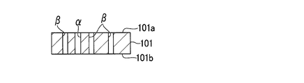
次に、図8Bに示すように、第二工程として、第一基板101の所定の位置にレーザーを照射することにより、改質部α、改質部βを形成する。
改質部αは、第一基板101内部のピンが形成される位置において、第一基板の一方の主面から他方の主面まで、すなわち、第一基板101の厚さと等しい長さ分の領域に形成する。
改質部βは、第一基板の導体柱が形成される位置において、第一基板の一方の主面から他方の主面まですなわち、第一基板101の厚さと等しい長さ分の領域に形成する。
なお、改質部βは径寸法dを有するとともに、隣接する改質部βとの距離Xが直径dよりも小さくなるように形成される。第一基板101は、例えばパイレックス(登録商標)から形成されてもよく、レーザー光としてパルス幅が250fsのフェムト秒レーザーを集光照射することにより改質部を形成する。上記の改質部α、βの寸法は、レーザー照射の条件により制御される。
第一工程におけるレーザーの照射方法について説明する。第一基板101の改質したい箇所にレーザー光12を照射するとともに、レーザー光12の焦点13を走査させる。この際、改質プロセスの進行に伴い、焦点13に至るレーザー光12の少なくとも一部が、先に形成された改質部、すなわちレーザー光12の照射によって改質された領域を伝播しないように、レーザー光12の焦点13を走査する。具体的には、図8Bに示す矢印の方向に、レーザー光12の焦点13を走査することにより第一基板101内部に改質部α、βを形成する。また、レーザー光12は、第一基板101の表面から内部に連続して、すなわち、一方の主面側から他方の主面側に向かって照射すると望ましい。
一般的に、レーザー光による改質部は第一基板101よりも高屈折率であるが、改質部とその近傍の屈折率分布は僅かに不均一であるため、改質部を伝播する光はランダムに反射、屈折する。したがって、第一基板101の内部においては、レーザー光12が集光部に伝播するまでに改質部を伝播することがないため、ビーム径が拡がるのを防止し、ピーク強度が小さくなるのを抑制することができる。また、レーザー光12の少なくとも一部が改質部14を伝播しないことにより、レーザー光12の照射によって改質される領域を早く形成することができる。
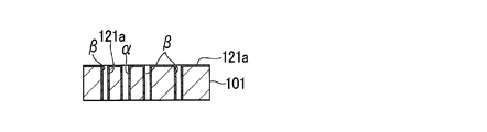
次いで、図8Cに示すように、第二工程として、改質部αおよび改質部βをエッチングにより除去する。エッチングは、容器(不図示)内に収容した所定の薬液中に改質部α、βが形成されたガラス基板101を浸漬することによって行う。これにより、改質部αおよび改質部βが、ガラス基板101の両側から薬液によりウェットエッチングされ、ガラス基板101の内部から除去される。
その結果として、図8Cに示すように、改質部αおよび改質部βが存在した部分に、第一貫通孔103および第二貫通孔104が形成される。本実施形態においては、薬液としてフッ酸を主成分とする酸溶液か、または、水酸化カリウムを主成分とする酸溶液を用いることができる。
なお、第二工程におけるエッチングは、改質されている部分が改質されていない部分に比べて非常に早くエッチングされる現象を利用する。これにより、改質部α、βの形状に起因した微細な第一貫通孔103、第二貫通孔104を形成することができる。本実施形態においては、微細な第一貫通孔103、第二貫通孔104の孔径は、製造する部分の用途に応じて、10μm~300μmの範囲で適宜決定することができる。
次いで、第三工程の前工程である下地形成工程として、図8Dに示すように、第一基板の一方の主面101a、第一貫通孔103および第二貫通孔104の内部にシード層121aを形成するとともに、図8Eに示すように、第一基板の他方の主面101bにシード層121bを形成する。シード層121a、121bは、いずれもスパッタリングによって形成することができ、CrとCuの混合物、TiとCuの混合物等からなり、厚みは10nm~500nm程度であることが望ましい。
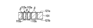
次いで、第三工程の前工程であるレジスト形成工程として、図8Fに示すように、シード層121a上における第一貫通孔の開口部103bに接続されるランドの形成領域の周囲に、めっきによるレジスト115aを形成する。また、シード層121b上における第一貫通孔の開口部103cと重なる領域の周囲に、めっきによるレジスト115bを形成する。
第一基板の一方の主面101a側からの平面視において、レジスト115aは円環状であり、第一貫通孔の開口部103bおよびランド123c部分を除いたアンチパッド111aに対応する領域を覆うよう形成される。また、第一基板の他方の主面101b側からの平面視において、レジスト115bは円環状であり、第一貫通孔の開口部103cを除いたアンチパッド112aに対応する領域を覆うように形成される。レジスト115aの内径寸法H3は、ランド123cの外径寸法H3を考慮して決定される。レジスト115a、115bとしては、例えば、液状ネガレジスト、フィルム状ネガレジスト、液状ポジレジスト、フィルム状ポジレジストを使用することができる。
次いで、第三工程として銅めっきを行い、図8Gに示すように、レジスト115に覆われた部分を除いたシード層121a、121bの表面に、めっき層を成長させる。以下では、第一基板の一方の主面101a側に形成されためっき層を接地導体層111、他方の主面101b側に形成されためっき層を接地導体層112、第一貫通孔103の内部に形成されためっき層をピン120、第二貫通孔104の内部に形成されためっき層を導体柱114と表記する。
めっき層の厚みは、少なくともミリ波帯の信号による表皮深さよりも厚いことが望ましい。60GHzの信号による表皮深さが270nmであることから、2μm程度とすれば十分と考えられる。なお、銅めっきによって形成されたピン120、導体柱114は、それぞれ、第一貫通孔103、第二貫通孔104の内部に完全に充填されていなくても良いが、気密性を要求される場合等には完全に充填されていることが望ましい。
次いで、レジスト剥離工程として、図8Hに示すように、レジスト115a、115bを剥離するとともに、残存するシード層121a、112bのエッチングを行う。これにより導体膜111、ランド123c、アンチパッド111a、112aを形成する。
次いで、第四工程として、図8Iに示すように、導体膜111上およびランド123cの外周部上に絶縁部124を形成する。絶縁部124は、第一貫通孔αの開口部と周囲のランド123cの中央側の円環部123eよりなる部分、および、平面回路(伝送線路)122終端部のGND接続ビア127となる部分と重なる部分において除去された開口部124a、124bを形成する。第一貫通孔103周辺の開口部は、径寸法がH2となるように決定され、これによって、図2に示すように、ランド123cに接続される部分の導体122aの外径寸法H2を決定する。
第四工程において形成する絶縁部124は、感光性樹脂からなり、例えば液状のものをスピンコート法によって、導体膜111および開口部部分のガラス基板表面111a上に塗布する。次いで、塗布された感光性樹脂層をキュアする際に、フォトリソグラフィー法により第一貫通孔103周辺の開口部124aと、GNDビア127となる開口部124bとを除去し、絶縁部124を形成する。
なお、フォトリソグラフィーによる樹脂除去工程時に、開口部124aにおいて円環部123e上の現像だけでは除去しきれない感光性樹脂残査が生じた場合、これらの除去には、CF4ガスやO2ガスによるRIE(Reactive Ion Etching)プロセスの実施が大変有効である。
次いで、伝送路形成工程の前工程である下地形成工程として、図8Kに示すように、シード層128を絶縁部124の表面と、ランド123cの円環部123eおよび孔αの内部と、開口部124b内部とに形成する。シード層128は、シード層121a、121bと同様に、スパッタリングによって形成することができ、CrとCuの混合物、TiとCuの混合物等からなり、厚みは10~500nm程度であることが望ましい。
次いで、伝送路形成工程の前工程であるレジスト形成工程として、図8Kに示すように、伝送路122を形成する部分以外のシード層128上に、めっきによるレジスト129を形成する。レジスト129は、伝送路122となる部分およびGSGパッド(不図示)、GNDパッド(不図示)、GNDビア(不図示)を形成する部分を除いた領域を覆うよう形成される。レジスト129の材料は、レジスト115a、115bと同様の材料であればよい。
次いで、レジスト剥離工程として、図8Mに示すように、レジスト129を剥離するとともに、残存するシード層128のエッチングをおこなう。これによりマイクロストリップラインを形成する伝送路122が形成される。
以上の工程を経ることによって、図1~3に示したモード変換器が得られる。なお、第一貫通孔および第二貫通孔を、上述したようにレーザーを用いて形成する場合には、第一基板を構成する部材が、レーザー光が透過可能なガラス等の部材に限定される。ただし、第一貫通孔および第二貫通孔は、ドライエッチング、ドリル等による機械的な加工によって形成することも可能であり、この場合には、第一基板を構成する部材が限定されることはない。また、第一基板の他方の主面101b側には、接地導体層112およびアンチパッド112aを被覆するパッシベーション膜を形成しても良い。絶縁部が形成されていることにより、接地導体層111、112およびアンチパッド111a、112aが異物付着、汚染等から保護される。また、モード変換器100に対して直に接するように、他の基板を積層することができる。パッシベーション膜としては、例えばポリイミド、シリコーン樹脂等の絶縁樹脂を利用することができる。
以上説明したように、本実施形態に係るモード変換器の製造方法によれば、ピンの入力インピーダンスを、基板の他方の主面に設けられたアンチパッドのサイズによって調整することができる。したがって、ピンを備えた第一貫通孔は少なくとも第一基板を貫通していればよく、その長さや、他の回路要素等に関する調整を行うことなく、反射損を抑制した信号伝送を実現してインピーダンス整合を取ることが可能となる。
また、本実施形態に係るモード変換器の製造方法によれば、アンチパッドはモード変換器の外側に露出した部位である。そのため、アンチパッドのサイズの微調整を目視で確認しながら行うことができる。そして、アンチパッドのサイズは、例えモード変換器が完成した後であっても、容易に再調整を行うこともできる。
さらに、本実施形態に係るモード変換器の製造方法によれば、第一基板として、複数の基材を積層した基板ではなく、単一の基材からなる基板を用いることができる。第一基板として単一の基材を用いることにより、複数の基材を積層する際、接着材による損失、各層の特性ばらつき、積層におけるズレ等の数々の好ましくない状況を全て回避することができる。
上述した実施形態においては、図3に示すように、第一基板の一方の主面101a側の端部から、他方の主面101b側の端部まで、ピン120の径寸法が均一である。
しかしながら、図9に示すように、第一基板の他方の主面101b側の端部123bを一方の主面101a側の端部123aよりも縮径させ、第一貫通孔103の側壁面が、第一基板の一方の主面101aと角度θ0をなすようにすることもできる。この場合、端部123b側から成膜加工したときに第一貫通孔103の内部における金属付着効果が向上するため、シード層121a、銅めっきの導体膜111を確実に形成することができる。
また、図10に示すように、第一貫通孔103について、第一基板の他方の主面101b側の端部123bを一方の主面101a側の端部123aよりも拡径させ、第一貫通孔103の側壁面が、第一基板の他方の主面101bと角度θ1をなすようにすることもできる。この場合、ピン120におけるミリ波信号を円滑に導入することができる。さらに、導波路への結合効率を高めることができるため、ミリ波信号を円滑に導入することできる。
また、図11に示すように、第一貫通孔103について、第一基板の他方の主面101b側の端部123bから一方の主面101a側の端部123aに向けて一旦縮径させてから拡径させ、第一貫通孔103の側壁面と第一基板の他方の主面101bとのなす角度を、端部123bにおいてはθ3、端部123aにおいてはθ4となるようにすることもできる。この場合、第一基板の両方の主面側から成膜加工したときに、第一貫通孔103の内部における金属付着効果が向上するため、シード層121a、銅めっきの導体膜111を確実に形成することができる。
本実施形態においては、ピン120から延伸された伝送線路122の終端はGSGパッド125となり、GNDパッド126にGND接続ビア127が隣接している。GND接続ビア127は、図4に示すように、GNDパッド126に対してGSGパッド125の反対側でもよい。しかし、図12に示すように、GNDパッド126に対してピン120から延長した伝送路122をさらに延長した位置のGND接続ビア127aでも、GNDパッド126に対してピン120側位置のGND接続ビア127bでもよい。また、GND接続ビア127は、GNDビア127a方向に任意の長さ分ずれた位置に配されていてもよいし、GND接続ビア127b方向に任意の長さ分ずれた位置に配されていてもよい。なお、図12では、GND接続ビアの位置を説明するために、GNDパッド126に対して位置の異なるGNDビアを複数記載した平面図である。
さらに、本実施形態においては、図1に示すように、導波路110が複数の導体柱114を有するとした。しかし、図11に示すように、平面視矩形をなす導波路110において、開口102に対向する後方壁となる辺は複数の導体柱140とし、また、ピン120から開口120に向かう方向に延在する2辺は、その方向に連続したスリット壁141とし、第一工程、第二工程において、連続した孔を形成することもできる。
後方壁となる辺を複数の導体柱140とすることにより、仮に、一部の導体柱において電気的にオープンとなる等の不具合が生じたとしても、残りの導体柱によって導波路110としての機能を維持することができる。導波路110の側壁を連続したスリット壁141として形成することにより、電磁波の漏洩を防止することができる。
また、本実施形態においては、図1に示すように、導波路110の側壁が、互いに離間して並ぶ複数の導体柱によって構成されていたが、図13に示すように、導波路の側壁は、一体化した導体によって構成されていてもよい。このような構成により、電磁波の進行方向の側壁が連続壁になっているため、ポスト配置が不連続であることによる電磁波の乱れを防止することができる。
また、上記のように第二貫通孔141を形成した場合、図14に示すように、多数の円柱を平面視して重なるように連続して形成したような形状とすることもできる。
さらに、図15に示すように、矩形の導波路110のうち開口102以外の三辺を連続する長孔β2を形成してU字形に連続するスリット壁142とするとともに、開口102付近のみ分離した導体柱140を有する導波路110とすることができる。この場合、ピン120周りの環境がポストではなく密閉空間となるので電磁波注入時のピン周りからの電磁波漏洩を阻止することができる。
また、図16に示すように、矩形の導波路110のうち開口102以外の三辺にそれぞれ連続する孔β1、β3を形成し、対応したスリット壁141、143とするとともに、各辺の交わる部分には導体柱140を設けて、導波路110が離間した状態を形成することができる。この場合、不連続部がポスト1個分のみであるため、不連続部における電磁波の乱れを最小限に抑えることができ、かつ、図15に示した構造よりも機械的に安定した構造が得られる。これらのように導波路110が、内側と外側で連続した状態を形成することによって、第一基板101が分離してしまうことがない。
また、図17に示すように、開口102の外側に、対向する導体柱114同士の距離が広がった形態のスリット壁144を設けることもできる。この場合、H面扇型ホーンアンテナを構成することができ、アンテナ利得を向上させることが可能となる。
上述した実施形態においては、図1~3に示すように、導体柱114の径寸法を第一基板101の一方の主面101aから他方の主面101bまで均一となるように決定した。しかし、図18に示すように、角度θ5を有するように主面101aから主面101bに向かって縮径するように形成することができる。この場合、孔β内部における金属付着効果を向上させて、シード層121a、銅めっきの導体柱を確実に形成することができる。また、角度θ5を有することにより、孔α内部における金属付着効果を向上させて、シード層121a、銅めっきの導体膜111を確実に形成することができる。
さらに、図19に示すように、導体柱114を、角度θ6、角度θ7を有するように表面101aから裏面101bに向けて、一旦縮径してから拡径するように形成することができる。角度θ6、角度θ7を有することにより、第一貫通孔103内部における金属付着効果を向上させて、シード層121a、銅めっきの導体膜111を確実に形成することができる。
また、導波路110では、図20に示すように、導体柱146の表面のみ、スリット壁147の表面のみに導体膜D1、D2を形成することもできる。つまり、対応する孔βおよび長孔β1の内部には導体がめっきによって充填されておらず、中空とされていてもよい。これらの場合、スリット壁147の対向する内面の間に対応する部分だけに導体膜111、112を設けることができる。この場合、導体柱146の両端は、確実に導体膜111、112と接続されることが好ましい。
このように、導波路110において、隙間のある導体柱114の一部について、スリット壁141、142、143、144、147を有する構造とすることで、導波路100を形成する導体膜111、112間の導波路110の大部分をスリット壁141、142、143、144、147に置き換えることができる。これにより、従来よりも大幅に電磁波の漏洩を抑えることができ、アンテナの放射効率の向上、および、導波路の放射損失を削減できる。また、スリット壁を採用することにより、導体柱114のみの場合よりも電流の流れる面積が大きくなる。したがって、すべてのポスト壁114の場合に起こりうるポスト壁114と導体膜111、112の電気的非導通による伝送モードの乱れ・破綻とそのリスクを大幅に軽減することが可能となる。
図21は、モード変換モジュール500の断面図である。図21に示すように、モード変換モジュール500は、無線送受信機能素子を有する無線通信IC(半導体チップ)510を、本実施形態のモード変換器100の平面回路122が配された側に、フリップチップ接続して構成される。
図3に示したモード変換器100を構成する第一基板101の一方の主面101aに、GNDを形成する導体膜111および絶縁部124上の伝送路122が設けられるとともに、これらと同階層に図示しない回路が設けられている。GSGパッドとして機能する伝送路の終端部125は、無線通信IC510の端子511と接続されている。ミリ波等の高い周波数の信号は、寄生インダクタンスの影響が非常に大きく受けるため、終端部125と端子511との接続は、ワイヤボンドよりもバンプを用いた短距離実装を行うことが望ましい。なお、電磁波導波部分の電磁界は外部環境からポストおよび連続壁によって遮断されているため、実装環境等の外部の影響を受けることはない。
図22は、モード変換モジュール550が第二基板(母基板、マザーボード)513に実装されている、モード変換ユニット600の断面図である。モード変換モジュール550は、モード変換器100を厚み方向に貫通する第三貫通孔605を有している。第三貫通孔605により、無線通信IC510と第二基板513とが電気的に接続されている。モード変換モジュール550と第二基板513との間には、アンダーフィル材(図示せず)が充填されていてもよい。アンダーフィル材によって、モード変換器100の接地導体層およびアンチパッドが被覆されるとともに、第一基板101と第二基板513とが接合された構成であってもよい。第三貫通孔605以外の構成要素は、図21のモード変換モジュール500と同様である。
図23は、図21のモード変換モジュール500とは異なる構成のモード変換モジュール560が第二基板(母基板、マザーボード)513に実装された、モード変換ユニット700の断面図である。モード変換モジュール560は、半導体チップ510を含んでおり、モード変換器100の表面に配された導体膜713bと半導体チップ510の端子(不図示)とがワイヤー512を介して電気的に接続されている。モード変換モジュール560は、モード変換器100を厚み方向に貫通する第三貫通孔705を有している。第三貫通孔705により、無線通信IC510と第二基板513とが電気的に接続されている。モード変換モジュール560と第二基板513との間には、アンダーフィル材(図示せず)が充填されていてもよい。アンダーフィル材によって、モード変換器100の接地導体層およびアンチパッドが被覆されるとともに、第一基板101と第二基板513とが接合された構成であってもよい。無線通信IC510、第三貫通孔705以外の構成要素は、図21のモード変換モジュール500と同様である。
以下、上記実施形態に係る実施例1~6を用いて、本発明をさらに具体的に説明するが、本発明が適用可能な実施例は、これに限定されるものではない。
実施例1
上述したモード変換器を用いた実施例1について説明する。本実施形態によるモード変換器(図5)を用いた場合と、従来技術によるモード変換器(図35)を用いた場合とについて、平面回路(高周波伝送路)からピンに伝播した信号のうち反射する成分(反射損失)に関するシミュレーションを行った。シミュレーションには3次元電磁界解析ソフトHFSSを用い、本実施形態、従来技術ともに第一基板の厚みを850μmにした。シミュレーションの結果を図24のグラフに示す。なお、本実施形態のモード変換器において、第一基板の他方のアンチパッドのサイズを100μmとした。
上述したモード変換器を用いた実施例1について説明する。本実施形態によるモード変換器(図5)を用いた場合と、従来技術によるモード変換器(図35)を用いた場合とについて、平面回路(高周波伝送路)からピンに伝播した信号のうち反射する成分(反射損失)に関するシミュレーションを行った。シミュレーションには3次元電磁界解析ソフトHFSSを用い、本実施形態、従来技術ともに第一基板の厚みを850μmにした。シミュレーションの結果を図24のグラフに示す。なお、本実施形態のモード変換器において、第一基板の他方のアンチパッドのサイズを100μmとした。
グラフの横軸は伝送回路からピンに伝播される信号の周波数を示し、縦軸は伝播した信号のピンにおける反射損失S11を示している。グラフ上の実線は本実施形態のモード変換器による結果に対応し、破線は従来技術のモード変換器による結果に対応している。グラフに示されるように、二本の線がほぼ一致していることから、本実施形態、従来技術のいずれのモード変換器においても、同様な反射損失の周波数依存性が得られることが分かった。これにより、本実施形態のように第一基板を貫通するようにピンを形成して、アンチパッドのサイズを調整することによって、従来技術のようにピン自体の長さを調整する場合と同様のレベルでのインピーダンス整合を実現できることが分かった。
実施例2
上述したモード変換器を用いた実施例2について説明する。本実施形態によるモード変換器(図5)を用いた場合と、従来技術によるモード変換器(図35)を用いた場合とについて、平面回路から伝播した信号のうち、第一基板の他方の主面301b側の開口部から漏洩する成分(伝送損失)に関するシミュレーションを行った。シミュレーションには3次元電磁界解析ソフトHFSSを用い、本実施形態、従来技術ともに第一基板の厚みを850μmにした。シミュレーションの結果を図25のグラフに示す。なお、本実施形態のモード変換器において、第一基板の他方のアンチパッドのサイズを100μmとした。
上述したモード変換器を用いた実施例2について説明する。本実施形態によるモード変換器(図5)を用いた場合と、従来技術によるモード変換器(図35)を用いた場合とについて、平面回路から伝播した信号のうち、第一基板の他方の主面301b側の開口部から漏洩する成分(伝送損失)に関するシミュレーションを行った。シミュレーションには3次元電磁界解析ソフトHFSSを用い、本実施形態、従来技術ともに第一基板の厚みを850μmにした。シミュレーションの結果を図25のグラフに示す。なお、本実施形態のモード変換器において、第一基板の他方のアンチパッドのサイズを100μmとした。
グラフの横軸は伝送回路からピンに伝播される信号の周波数を示し、縦軸は伝播した信号のピンからの伝送損失S21を示している。グラフ上の実線は本実施形態のモード変換器による結果に対応し、破線は従来技術のモード変換器による結果に対応している。グラフに示されるように、二本の線がほぼ一致していることから、本実施形態、従来技術のいずれのモード変換器においても、同様な伝送損失の周波数依存性が得られることが分かった。これにより、本実施形態のように、ピンが第一基板を貫通させる構造をとることにより、ピンの内部の空間が外部に対して開放されている場合であっても、従来技術のように、ピンの内部の空間が第一基板の内部に密閉されている場合と同等に抑えられることが分かった。
実施例3
上述したモード変換器を用いた実施例3について説明する。本実施形態によるモード変換器(図5)を用いた場合と、従来技術によるモード変換器(図35)を用いた場合とについて、モード変換器を動作させた際に、第一基板内部において発生する電界の分布に関するシミュレーションを行った。シミュレーションには3次元電磁界解析ソフトHFSSを用い、本実施形態、従来技術ともに第一基板の厚みを850μmにした。従来技術によるシミュレーション結果、本実施形態によるシミュレーション結果を、それぞれ図26A、図26Bに示す。ただし、実際には電界分布は時間的に変動しており、これらは、ある瞬間の電界分布を示したグラフである。
上述したモード変換器を用いた実施例3について説明する。本実施形態によるモード変換器(図5)を用いた場合と、従来技術によるモード変換器(図35)を用いた場合とについて、モード変換器を動作させた際に、第一基板内部において発生する電界の分布に関するシミュレーションを行った。シミュレーションには3次元電磁界解析ソフトHFSSを用い、本実施形態、従来技術ともに第一基板の厚みを850μmにした。従来技術によるシミュレーション結果、本実施形態によるシミュレーション結果を、それぞれ図26A、図26Bに示す。ただし、実際には電界分布は時間的に変動しており、これらは、ある瞬間の電界分布を示したグラフである。
なお、モード変換器300内部に生じる電界分布を示すために、導体柱314、伝送路322、ピン320、ランド323cおよび322b、アンチパッド312a以外の構成要素は図示していない。本実施形態のモード変換器においては、アンチパッド312aのサイズを100μmとした。
ピンの開口部303bから図2で示すGSGパッド125へ向かう方向をy軸、第一基板の両方の主面301a、301bと平行な面内においてy軸と90度なす方向をx軸、第一基板の他方の主面301bから一方の主面301aに向かう方向をz軸とした。図26A、図26Bのいずれのシミュレーション結果においても、ピンの近傍に電界の最も強い箇所が存在し、最も強い箇所からの距離に反比例して電界が弱くなって行く分布が見られた。そして、電界の強い箇所は、ピン120から遠ざかる(-y)方向に、一定間隔おきに周期的に並んでおり、各々の箇所において同様の分布が見られた。図26A、図26Bを用いて、ピンから等距離の位置同士でシミュレーション結果を比較すると、両者の電界分布はほぼ一致していることが分かった。
実施例4
上述したモード変換器を用いた実施例4について説明する。本実施形態によるモード変換器(図5)を用いた場合について、平面回路からピンに励振した信号のうち反射する比率(反射損失)に関するシミュレーションを、異なるサイズのアンチパッドを用いて行った。本実施例において、アンチパッド312aは、円形リング形状であり、外径と内径との差H4が30μm以上90μm未満の範囲で10μmずつ異なるサイズとした。図27に、アンチパッド312aの形状を模式的に示す。なお、ここではアンチパッドによる容量値を制御するための円形リング形状のランド322bも、ピン先端に形成されている。従って、ここでは、H4はランド322bの外径とアンチパッド312aの外径との差ともいえる。ランド322bの外径はピン320の外径よりも大きく、ランド322bの中心がピンの中心に一致するように配置されている。モード変換器300の動作時には、ランド322bの外周面から接地導体層312に対して、基板301の厚み方向に垂直な方向の電界が発生する。なお、TEモードの電磁波の進む方向は矢印で示されている。円形のアンチパッドを用いることで、基板と導体との間の応力を低減することができ、また、本実施例のピンの先端構造を容易に製造することができる。
シミュレーションには3次元電磁界解析ソフトHFSSを用い、本実施形態、従来技術ともに第一基板の厚みを850μmにした。また、第一貫通孔303の内部には樹脂を充填し、樹脂を比誘電率3.4の誘電体としてシミュレーションした。この結果を図28のグラフに示す。
上述したモード変換器を用いた実施例4について説明する。本実施形態によるモード変換器(図5)を用いた場合について、平面回路からピンに励振した信号のうち反射する比率(反射損失)に関するシミュレーションを、異なるサイズのアンチパッドを用いて行った。本実施例において、アンチパッド312aは、円形リング形状であり、外径と内径との差H4が30μm以上90μm未満の範囲で10μmずつ異なるサイズとした。図27に、アンチパッド312aの形状を模式的に示す。なお、ここではアンチパッドによる容量値を制御するための円形リング形状のランド322bも、ピン先端に形成されている。従って、ここでは、H4はランド322bの外径とアンチパッド312aの外径との差ともいえる。ランド322bの外径はピン320の外径よりも大きく、ランド322bの中心がピンの中心に一致するように配置されている。モード変換器300の動作時には、ランド322bの外周面から接地導体層312に対して、基板301の厚み方向に垂直な方向の電界が発生する。なお、TEモードの電磁波の進む方向は矢印で示されている。円形のアンチパッドを用いることで、基板と導体との間の応力を低減することができ、また、本実施例のピンの先端構造を容易に製造することができる。
シミュレーションには3次元電磁界解析ソフトHFSSを用い、本実施形態、従来技術ともに第一基板の厚みを850μmにした。また、第一貫通孔303の内部には樹脂を充填し、樹脂を比誘電率3.4の誘電体としてシミュレーションした。この結果を図28のグラフに示す。
グラフの横軸は伝送回路からピンに伝播される信号の周波数を示し、縦軸は伝播した信号のピンにおける反射損失S11を示している。モード変換器として十分な反射損失S11を約-15dB以下として、-15dBを閾値とする。また、使用周波数帯域を約57~66GHzとする。
グラフに示す結果から、反射損失の大きさは、アンチパッドのサイズによって変化することが分かった。上記使用周波数帯域で閾値以下の反射損失を示したのは、H4が50μm以上80μm未満のアンチパッドを形成した場合である。したがって、アンチパッドのサイズ(すなわち、H4)を50μm以上80μm未満とすることが好ましい。これによって、ピンにおける反射損失の制御、すなわちピンにおけるインピーダンスを平面回路のインピーダンスと整合させる制御が可能であることが分かった。
実施例5
第一貫通孔303の内部を誘電体で充填しないこと以外は、実施例4と同様のモード変換器を用いて、同様の実験条件のもとで、シミュレーションを行った。シミュレーションの結果を図29のグラフに示す。
第一貫通孔303の内部を誘電体で充填しないこと以外は、実施例4と同様のモード変換器を用いて、同様の実験条件のもとで、シミュレーションを行った。シミュレーションの結果を図29のグラフに示す。
グラフに示す結果から、反射損失の大きさは、アンチパッドのサイズによって変化することが分かった。上記使用周波数帯域で閾値以下の反射損失を示したのは、H4が40μm以上80μm未満のアンチパッドを形成した場合である。したがって、アンチパッドのサイズ(すなわち、H4)を40μm以上80μm未満とすることが好ましい。これによって、誘電体で充填しない場合であっても、ピンにおける反射損失の制御、すなわちピンにおけるインピーダンスを平面回路のインピーダンスと整合させる制御が可能であることが分かった。
実施例6
矩形リング形状のアンチパッド312aを用いて、実施例4と同様のシミュレーションを行った。実施例4と同様のモード変換器を用い、実験条件も同様である。図30に、アンチパッドの形状を模式的に示す。シミュレーションに用いた矩形リング形状のアンチパッド312aは、図5に示す幅H4が40μm以上120μm未満の範囲において、40,50,60,80,120μmとした。なお、ここではアンチパッドによる容量値を制御するための矩形リング形状のランド322bも、ピン320の先端に形成されている。従って、ここでは、H4はランド322bの一辺と絶縁する領域を挟んで対向する接地導体層312の一辺との間の距離である。ランド322bの中心から外枠までの長さはピン320の外径よりも大きく、ランド322bの中心がピン320の中心に一致するように配置されている。モード変換器300の動作時には、ランド322bの外周面から接地導体層312に対して、基板301の厚み方向に垂直な方向の電界が発生する。矩形のアンチパッドを用いると、基板の厚み方向に対して垂直な方向の成分(横向き成分)を多く含む向きの電界が発生するので、より効率よくTEモードを誘起することができる。ここで、TEモードの電磁波の進む方向は矢印で示されている。また、横向き成分を効率よく発生させるために、ランド322bの一辺と矩形のアンチパッド312aの外枠の一辺とが、H4の間隔を空けて互いに平行、かつ、矢印で示すTEモードの電磁波の進む方向と垂直であるように配置されることが好ましい。
矩形リング形状のアンチパッド312aを用いて、実施例4と同様のシミュレーションを行った。実施例4と同様のモード変換器を用い、実験条件も同様である。図30に、アンチパッドの形状を模式的に示す。シミュレーションに用いた矩形リング形状のアンチパッド312aは、図5に示す幅H4が40μm以上120μm未満の範囲において、40,50,60,80,120μmとした。なお、ここではアンチパッドによる容量値を制御するための矩形リング形状のランド322bも、ピン320の先端に形成されている。従って、ここでは、H4はランド322bの一辺と絶縁する領域を挟んで対向する接地導体層312の一辺との間の距離である。ランド322bの中心から外枠までの長さはピン320の外径よりも大きく、ランド322bの中心がピン320の中心に一致するように配置されている。モード変換器300の動作時には、ランド322bの外周面から接地導体層312に対して、基板301の厚み方向に垂直な方向の電界が発生する。矩形のアンチパッドを用いると、基板の厚み方向に対して垂直な方向の成分(横向き成分)を多く含む向きの電界が発生するので、より効率よくTEモードを誘起することができる。ここで、TEモードの電磁波の進む方向は矢印で示されている。また、横向き成分を効率よく発生させるために、ランド322bの一辺と矩形のアンチパッド312aの外枠の一辺とが、H4の間隔を空けて互いに平行、かつ、矢印で示すTEモードの電磁波の進む方向と垂直であるように配置されることが好ましい。
シミュレーションの結果を図31のグラフに示す。
グラフに示す結果から、矩形リング形状のアンチパッドを用いた場合でも、反射損失の大きさは、アンチパッドのサイズによって変化することが分かった。H4が40~120μmの全ての範囲において、上記使用周波数帯域で閾値以下の反射損失を示した。したがって、アンチパッドのサイズを40~120μmとすることが好ましい。これによって、ピンにおける反射損失の制御、すなわちピンにおけるインピーダンスを平面回路のインピーダンスと整合させる制御が可能であることが分かった。
グラフに示す結果から、矩形リング形状のアンチパッドを用いた場合でも、反射損失の大きさは、アンチパッドのサイズによって変化することが分かった。H4が40~120μmの全ての範囲において、上記使用周波数帯域で閾値以下の反射損失を示した。したがって、アンチパッドのサイズを40~120μmとすることが好ましい。これによって、ピンにおける反射損失の制御、すなわちピンにおけるインピーダンスを平面回路のインピーダンスと整合させる制御が可能であることが分かった。
実施例7
第一貫通孔203の内部を誘電体で充填しないこと以外は、実施例6と同様のモード変換器を用いて、同様の実験条件のもとで、シミュレーションを行った。シミュレーションの結果を図32のグラフに示す。
第一貫通孔203の内部を誘電体で充填しないこと以外は、実施例6と同様のモード変換器を用いて、同様の実験条件のもとで、シミュレーションを行った。シミュレーションの結果を図32のグラフに示す。
グラフに示す結果から、反射損失の大きさは、アンチパッドのサイズによって変化することが分かった。H4が40~120μmの全ての範囲において、上記使用周波数帯域で閾値以下の反射損失を示した。したがって、アンチパッドのサイズを40~120μmとすることが好ましい。これによって、誘電体で充填しない場合であっても、ピンにおける反射損失の制御、すなわちピンにおけるインピーダンスを平面回路のインピーダンスと整合させる制御が可能であることが分かった。
以上、本発明の好ましい実施例を説明したが、本発明はこれら実施例に限定されることはない。本発明の趣旨を逸脱しない範囲で、構成の付加、省略、置換、およびその他の変更が可能である。
本発明は、ミリ波帯を利用した数Gbpsの高速大容量通信用のデバイスとして、広く適用することができる。
100、200、300 モード変換器
101、201、301 第一基板
101a、101b、201a、201b、301a、301b 主面
101c 一端
102 第二基板
103 第一貫通孔
103a 内壁面
103b、103c 開口部
104 第二貫通孔
110、210、310 導波路
111、112、211、212、311、312 接地導体層(導体膜)
111a、112a、212a、212b、312a、312b アンチパッド
114、214、314 導体柱
122a、222a、322a 導体
122f、123f 導体膜
120、220、320 ピン
123c、223c、323c ランド
123d、223d、323d 外縁部
123e、223e、323e 円環部
101、201、301 第一基板
101a、101b、201a、201b、301a、301b 主面
101c 一端
102 第二基板
103 第一貫通孔
103a 内壁面
103b、103c 開口部
104 第二貫通孔
110、210、310 導波路
111、112、211、212、311、312 接地導体層(導体膜)
111a、112a、212a、212b、312a、312b アンチパッド
114、214、314 導体柱
122a、222a、322a 導体
122f、123f 導体膜
120、220、320 ピン
123c、223c、323c ランド
123d、223d、323d 外縁部
123e、223e、323e 円環部
Claims (10)
- 第一主面および第二主面を有する基板と、
前記第一主面に形成された第一接地導体層と、
前記第二主面に形成された第二接地導体層と、
前記第一主面に形成された、高周波を伝播する平面回路と、
前記平面回路と接続され、前記第一主面から前記第二主面まで貫通する貫通孔の内部に形成され、前記第一主面および前記第二主面に連通するピンと、
前記第二主面において露出した前記ピンの端部と、前記第二接地導体層との間に形成されたアンチパッドと、
を備えるモード変換器。 - 前記ピンは、前記第二主面上に延設されている、請求項1に記載のモード変換器。
- 前記ピンは、前記貫通孔の内壁に沿って形成され、円筒形を有する、請求項1または2に記載のモード変換器。
- 前記アンチパッドは、円形リング形状を有する、請求項1~3のいずれか1項に記載のモード変換器。
- 前記円形リング形状を有する前記アンチパッドの、外径と内径との差が、40~80μmである、請求項4に記載のモード変換器。
- 前記貫通孔には、誘電体が充填されている、請求項4に記載のモード変換器。
- 前記円形リング形状を有する前記アンチパッドの、外径と内径との差が、50~80μmである、請求項6に記載のモード変換器。
- 前記アンチパッドは、矩形リング形状を有する、請求項1~3のいずれか1項に記載のモード変換器。
- 前記貫通孔には、誘電体が充填されている、請求項8に記載のモード変換器。
- 前記矩形リング形状を有する前記アンチパッドの、矩形リングの外側の一辺と内側の一辺との間の長さが、40~120μmである、請求項8または9に記載のモード変換器。
Priority Applications (4)
| Application Number | Priority Date | Filing Date | Title |
|---|---|---|---|
| EP13866566.6A EP2940784B1 (en) | 2012-12-27 | 2013-12-27 | Mode converter |
| JP2014554609A JP5947917B2 (ja) | 2012-12-27 | 2013-12-27 | モード変換器 |
| CN201380068055.XA CN104904061B (zh) | 2012-12-27 | 2013-12-27 | 模式转换器 |
| US14/749,839 US9812755B2 (en) | 2012-12-27 | 2015-06-25 | Mode converter between a plane circuit and a substrate waveguide including a pin having a land and an anti-pad |
Applications Claiming Priority (2)
| Application Number | Priority Date | Filing Date | Title |
|---|---|---|---|
| JP2012283993 | 2012-12-27 | ||
| JP2012-283993 | 2012-12-27 |
Related Child Applications (1)
| Application Number | Title | Priority Date | Filing Date |
|---|---|---|---|
| US14/749,839 Continuation US9812755B2 (en) | 2012-12-27 | 2015-06-25 | Mode converter between a plane circuit and a substrate waveguide including a pin having a land and an anti-pad |
Publications (1)
| Publication Number | Publication Date |
|---|---|
| WO2014104336A1 true WO2014104336A1 (ja) | 2014-07-03 |
Family
ID=51021400
Family Applications (1)
| Application Number | Title | Priority Date | Filing Date |
|---|---|---|---|
| PCT/JP2013/085201 Ceased WO2014104336A1 (ja) | 2012-12-27 | 2013-12-27 | モード変換器 |
Country Status (5)
| Country | Link |
|---|---|
| US (1) | US9812755B2 (ja) |
| EP (1) | EP2940784B1 (ja) |
| JP (1) | JP5947917B2 (ja) |
| CN (1) | CN104904061B (ja) |
| WO (1) | WO2014104336A1 (ja) |
Cited By (10)
| Publication number | Priority date | Publication date | Assignee | Title |
|---|---|---|---|---|
| JP2014158243A (ja) * | 2013-02-18 | 2014-08-28 | Fujikura Ltd | モード変換器の製造方法 |
| JP6054501B1 (ja) * | 2015-12-17 | 2016-12-27 | 株式会社フジクラ | 終端装置および終端方法 |
| EP3176868A4 (en) * | 2014-07-30 | 2017-08-16 | Fujitsu Ltd. | Electronic device and electronic device manufacturing method |
| JP2017228847A (ja) * | 2016-06-20 | 2017-12-28 | 株式会社フジクラ | 導波路、モード変換器、及び導波路の製造方法 |
| JP2017228826A (ja) * | 2016-06-20 | 2017-12-28 | 株式会社フジクラ | 導波路および導波路の製造方法 |
| US9881860B2 (en) * | 2015-06-17 | 2018-01-30 | Fujikura Ltd. | Method for producing waveguide substrate |
| JP2020502937A (ja) * | 2016-12-23 | 2020-01-23 | ティーイー コネクティビティ ネーデルランド ビーヴイTE Connectivity Nederland BV | ミリ波アンテナおよび接続装置 |
| WO2020230608A1 (ja) * | 2019-05-10 | 2020-11-19 | 株式会社フジクラ | モード変換器 |
| WO2022004545A1 (ja) * | 2020-06-30 | 2022-01-06 | 株式会社村田製作所 | 導波路 |
| JPWO2024095892A1 (ja) * | 2022-10-31 | 2024-05-10 |
Families Citing this family (5)
| Publication number | Priority date | Publication date | Assignee | Title |
|---|---|---|---|---|
| JP6177952B1 (ja) * | 2016-02-26 | 2017-08-09 | 株式会社フジクラ | フィルタ及びそのフィルタの設計方法 |
| JP2020198595A (ja) * | 2019-06-05 | 2020-12-10 | 株式会社フジクラ | モード変換器 |
| JP6767591B1 (ja) * | 2019-06-10 | 2020-10-14 | 株式会社フジクラ | モード変換器、rfモジュール、及び携帯端末 |
| CN115335982B (zh) * | 2020-01-16 | 2025-06-24 | 株式会社藤仓 | 基板和天线模块 |
| US12451578B2 (en) * | 2022-12-30 | 2025-10-21 | Nxp B.V. | Interposers with millimeter-wave coaxial-to-waveguide transistions |
Citations (4)
| Publication number | Priority date | Publication date | Assignee | Title |
|---|---|---|---|---|
| JP2005051331A (ja) * | 2003-07-29 | 2005-02-24 | Kyocera Corp | マイクロストリップ線路と誘電体導波管との結合構造 |
| JP2011082337A (ja) | 2009-10-07 | 2011-04-21 | Panasonic Corp | インダクタンス素子 |
| JP2011109438A (ja) | 2009-11-18 | 2011-06-02 | Amushisu:Kk | アンテナモジュール及びアンテナモジュールを有する無線デバイス。 |
| US20110267152A1 (en) * | 2010-04-30 | 2011-11-03 | Samsung Electro-Mechanics Co., Ltd. | Wideband transmission line - waveguide transition apparatus |
Family Cites Families (7)
| Publication number | Priority date | Publication date | Assignee | Title |
|---|---|---|---|---|
| US5045820A (en) * | 1989-09-27 | 1991-09-03 | Motorola, Inc. | Three-dimensional microwave circuit carrier and integral waveguide coupler |
| US7215007B2 (en) * | 2003-06-09 | 2007-05-08 | Wemtec, Inc. | Circuit and method for suppression of electromagnetic coupling and switching noise in multilayer printed circuit boards |
| FR2951321B1 (fr) * | 2009-10-08 | 2012-03-16 | St Microelectronics Sa | Dispositif semi-conducteur comprenant un guide d'ondes electro-magnetiques |
| FR2953651B1 (fr) * | 2009-12-07 | 2012-01-20 | Eads Defence & Security Sys | Dispositif de transition hyperfrequence entre une ligne a micro-ruban et un guide d'onde rectangulaire |
| US8823470B2 (en) * | 2010-05-17 | 2014-09-02 | Cts Corporation | Dielectric waveguide filter with structure and method for adjusting bandwidth |
| CN102214624B (zh) * | 2011-05-17 | 2013-05-29 | 北京大学 | 一种具有通孔的半导体结构及其制造方法 |
| JP5948844B2 (ja) * | 2011-12-14 | 2016-07-06 | ソニー株式会社 | 導波路およびこれを備えたインターポーザ基板ならびにモジュールおよび電子機器 |
-
2013
- 2013-12-27 CN CN201380068055.XA patent/CN104904061B/zh active Active
- 2013-12-27 JP JP2014554609A patent/JP5947917B2/ja active Active
- 2013-12-27 WO PCT/JP2013/085201 patent/WO2014104336A1/ja not_active Ceased
- 2013-12-27 EP EP13866566.6A patent/EP2940784B1/en active Active
-
2015
- 2015-06-25 US US14/749,839 patent/US9812755B2/en active Active
Patent Citations (4)
| Publication number | Priority date | Publication date | Assignee | Title |
|---|---|---|---|---|
| JP2005051331A (ja) * | 2003-07-29 | 2005-02-24 | Kyocera Corp | マイクロストリップ線路と誘電体導波管との結合構造 |
| JP2011082337A (ja) | 2009-10-07 | 2011-04-21 | Panasonic Corp | インダクタンス素子 |
| JP2011109438A (ja) | 2009-11-18 | 2011-06-02 | Amushisu:Kk | アンテナモジュール及びアンテナモジュールを有する無線デバイス。 |
| US20110267152A1 (en) * | 2010-04-30 | 2011-11-03 | Samsung Electro-Mechanics Co., Ltd. | Wideband transmission line - waveguide transition apparatus |
Non-Patent Citations (3)
| Title |
|---|
| E.ARNIERI ET AL.: "Coaxially fed substrate integrated radiating waveguides", ANTENNAS AND PROPAGATION SOCIETY INTERNATIONAL SYMPOSIUM, 2007, pages 2718 - 2721, XP031169740 * |
| R. SUGA ET AL.: "Cost-Effective 60-GHz Antenna-Package with End-Fire Radiation from Open-Ended Post-Wall Waveguide for Wireless File-Transfer System", IEEE MTT-S INTERNATIONAL MICROWAVE SYMPOSIUM, 2011, pages 348 - 351 |
| See also references of EP2940784A4 |
Cited By (16)
| Publication number | Priority date | Publication date | Assignee | Title |
|---|---|---|---|---|
| US10511077B2 (en) | 2013-02-18 | 2019-12-17 | Fujikura Ltd. | Method for manufacturing mode converter |
| JP2014158243A (ja) * | 2013-02-18 | 2014-08-28 | Fujikura Ltd | モード変換器の製造方法 |
| US10389006B2 (en) | 2014-07-30 | 2019-08-20 | Fujitsu Limited | Electronic apparatus and manufacturing method thereof |
| EP3176868A4 (en) * | 2014-07-30 | 2017-08-16 | Fujitsu Ltd. | Electronic device and electronic device manufacturing method |
| US9881860B2 (en) * | 2015-06-17 | 2018-01-30 | Fujikura Ltd. | Method for producing waveguide substrate |
| JP6054501B1 (ja) * | 2015-12-17 | 2016-12-27 | 株式会社フジクラ | 終端装置および終端方法 |
| US10003115B2 (en) | 2015-12-17 | 2018-06-19 | Fujikura Ltd. | Terminator and termination method |
| JP2017228826A (ja) * | 2016-06-20 | 2017-12-28 | 株式会社フジクラ | 導波路および導波路の製造方法 |
| JP2017228847A (ja) * | 2016-06-20 | 2017-12-28 | 株式会社フジクラ | 導波路、モード変換器、及び導波路の製造方法 |
| JP2020502937A (ja) * | 2016-12-23 | 2020-01-23 | ティーイー コネクティビティ ネーデルランド ビーヴイTE Connectivity Nederland BV | ミリ波アンテナおよび接続装置 |
| WO2020230608A1 (ja) * | 2019-05-10 | 2020-11-19 | 株式会社フジクラ | モード変換器 |
| US11843157B2 (en) | 2019-05-10 | 2023-12-12 | Fujikura Ltd. | Mode converter for converting modes between a post-wall waveguide and a microstrip line using an excitation pin and anti-pads |
| WO2022004545A1 (ja) * | 2020-06-30 | 2022-01-06 | 株式会社村田製作所 | 導波路 |
| JPWO2024095892A1 (ja) * | 2022-10-31 | 2024-05-10 | ||
| WO2024095892A1 (ja) * | 2022-10-31 | 2024-05-10 | 京セラ株式会社 | 印刷配線板及びその製造方法 |
| JP7770590B2 (ja) | 2022-10-31 | 2025-11-14 | 京セラ株式会社 | 印刷配線板及びその製造方法 |
Also Published As
| Publication number | Publication date |
|---|---|
| EP2940784A4 (en) | 2016-08-17 |
| US20150295295A1 (en) | 2015-10-15 |
| EP2940784B1 (en) | 2022-08-24 |
| JP5947917B2 (ja) | 2016-07-06 |
| CN104904061A (zh) | 2015-09-09 |
| JPWO2014104336A1 (ja) | 2017-01-19 |
| US9812755B2 (en) | 2017-11-07 |
| EP2940784A1 (en) | 2015-11-04 |
| CN104904061B (zh) | 2017-07-21 |
Similar Documents
| Publication | Publication Date | Title |
|---|---|---|
| JP5947917B2 (ja) | モード変換器 | |
| EP2958188B1 (en) | Mode converter and production method therefor | |
| CN101772859B (zh) | 波导管的连接结构 | |
| US9577340B2 (en) | Waveguide adapter plate to facilitate accurate alignment of sectioned waveguide channel in microwave antenna assembly | |
| US9515385B2 (en) | Coplanar waveguide implementing launcher and waveguide channel section in IC package substrate | |
| JP2014236291A (ja) | モード変換器 | |
| US9520635B2 (en) | RF system-in-package with microstrip-to-waveguide transition | |
| JP5531960B2 (ja) | 導波管接続構造および導波管接続方法 | |
| EP3890113B1 (en) | Waveguide slot antenna | |
| JP5702418B2 (ja) | モード変換器 | |
| JP6182422B2 (ja) | 導波管との接続構造 | |
| US10325850B1 (en) | Ground pattern for solderability and radio-frequency properties in millimeter-wave packages | |
| US10861805B2 (en) | High frequency module | |
| JP2011172173A (ja) | ミリ波回路モジュール及びそれを用いたミリ波送受信機 | |
| CN220324682U (zh) | 射频信号传输结构 | |
| US20260107384A1 (en) | Circuit board structure | |
| US20260096439A1 (en) | Laminate substrate for a radiofrequency device | |
| US20260094973A1 (en) | Laminate substrate for a radiofrequency device | |
| JP2015089091A (ja) | モード変換器の製造方法 | |
| WO2025219644A1 (en) | A radio frequency interface and a waveguide module | |
| JP5764639B2 (ja) | モード変換器 |
Legal Events
| Date | Code | Title | Description |
|---|---|---|---|
| 121 | Ep: the epo has been informed by wipo that ep was designated in this application |
Ref document number: 13866566 Country of ref document: EP Kind code of ref document: A1 |
|
| ENP | Entry into the national phase |
Ref document number: 2014554609 Country of ref document: JP Kind code of ref document: A |
|
| NENP | Non-entry into the national phase |
Ref country code: DE |
|
| WWE | Wipo information: entry into national phase |
Ref document number: 2013866566 Country of ref document: EP |