WO2014119002A1 - 液晶表示装置及びカラーフィルタ基板 - Google Patents
液晶表示装置及びカラーフィルタ基板 Download PDFInfo
- Publication number
- WO2014119002A1 WO2014119002A1 PCT/JP2013/057556 JP2013057556W WO2014119002A1 WO 2014119002 A1 WO2014119002 A1 WO 2014119002A1 JP 2013057556 W JP2013057556 W JP 2013057556W WO 2014119002 A1 WO2014119002 A1 WO 2014119002A1
- Authority
- WO
- WIPO (PCT)
- Prior art keywords
- filter
- liquid crystal
- color filter
- layer
- substrate
- Prior art date
- Legal status (The legal status is an assumption and is not a legal conclusion. Google has not performed a legal analysis and makes no representation as to the accuracy of the status listed.)
- Ceased
Links
Images


Classifications
-
- G—PHYSICS
- G06—COMPUTING OR CALCULATING; COUNTING
- G06F—ELECTRIC DIGITAL DATA PROCESSING
- G06F3/00—Input arrangements for transferring data to be processed into a form capable of being handled by the computer; Output arrangements for transferring data from processing unit to output unit, e.g. interface arrangements
- G06F3/01—Input arrangements or combined input and output arrangements for interaction between user and computer
- G06F3/03—Arrangements for converting the position or the displacement of a member into a coded form
- G06F3/041—Digitisers, e.g. for touch screens or touch pads, characterised by the transducing means
- G06F3/044—Digitisers, e.g. for touch screens or touch pads, characterised by the transducing means by capacitive means
- G06F3/0446—Digitisers, e.g. for touch screens or touch pads, characterised by the transducing means by capacitive means using a grid-like structure of electrodes in at least two directions, e.g. using row and column electrodes
-
- G—PHYSICS
- G02—OPTICS
- G02B—OPTICAL ELEMENTS, SYSTEMS OR APPARATUS
- G02B5/00—Optical elements other than lenses
- G02B5/20—Filters
- G02B5/201—Filters in the form of arrays
-
- G—PHYSICS
- G02—OPTICS
- G02B—OPTICAL ELEMENTS, SYSTEMS OR APPARATUS
- G02B5/00—Optical elements other than lenses
- G02B5/20—Filters
- G02B5/22—Absorbing filters
- G02B5/223—Absorbing filters containing organic substances, e.g. dyes, inks or pigments
-
- G—PHYSICS
- G02—OPTICS
- G02F—OPTICAL DEVICES OR ARRANGEMENTS FOR THE CONTROL OF LIGHT BY MODIFICATION OF THE OPTICAL PROPERTIES OF THE MEDIA OF THE ELEMENTS INVOLVED THEREIN; NON-LINEAR OPTICS; FREQUENCY-CHANGING OF LIGHT; OPTICAL LOGIC ELEMENTS; OPTICAL ANALOGUE/DIGITAL CONVERTERS
- G02F1/00—Devices or arrangements for the control of the intensity, colour, phase, polarisation or direction of light arriving from an independent light source, e.g. switching, gating or modulating; Non-linear optics
- G02F1/01—Devices or arrangements for the control of the intensity, colour, phase, polarisation or direction of light arriving from an independent light source, e.g. switching, gating or modulating; Non-linear optics for the control of the intensity, phase, polarisation or colour
- G02F1/13—Devices or arrangements for the control of the intensity, colour, phase, polarisation or direction of light arriving from an independent light source, e.g. switching, gating or modulating; Non-linear optics for the control of the intensity, phase, polarisation or colour based on liquid crystals, e.g. single liquid crystal display cells
- G02F1/133—Constructional arrangements; Operation of liquid crystal cells; Circuit arrangements
- G02F1/1333—Constructional arrangements; Manufacturing methods
- G02F1/13338—Input devices, e.g. touch panels
-
- G—PHYSICS
- G02—OPTICS
- G02F—OPTICAL DEVICES OR ARRANGEMENTS FOR THE CONTROL OF LIGHT BY MODIFICATION OF THE OPTICAL PROPERTIES OF THE MEDIA OF THE ELEMENTS INVOLVED THEREIN; NON-LINEAR OPTICS; FREQUENCY-CHANGING OF LIGHT; OPTICAL LOGIC ELEMENTS; OPTICAL ANALOGUE/DIGITAL CONVERTERS
- G02F1/00—Devices or arrangements for the control of the intensity, colour, phase, polarisation or direction of light arriving from an independent light source, e.g. switching, gating or modulating; Non-linear optics
- G02F1/01—Devices or arrangements for the control of the intensity, colour, phase, polarisation or direction of light arriving from an independent light source, e.g. switching, gating or modulating; Non-linear optics for the control of the intensity, phase, polarisation or colour
- G02F1/13—Devices or arrangements for the control of the intensity, colour, phase, polarisation or direction of light arriving from an independent light source, e.g. switching, gating or modulating; Non-linear optics for the control of the intensity, phase, polarisation or colour based on liquid crystals, e.g. single liquid crystal display cells
- G02F1/133—Constructional arrangements; Operation of liquid crystal cells; Circuit arrangements
- G02F1/1333—Constructional arrangements; Manufacturing methods
- G02F1/1335—Structural association of cells with optical devices, e.g. polarisers or reflectors
- G02F1/133509—Filters, e.g. light shielding masks
- G02F1/133512—Light shielding layers, e.g. black matrix
-
- G—PHYSICS
- G02—OPTICS
- G02F—OPTICAL DEVICES OR ARRANGEMENTS FOR THE CONTROL OF LIGHT BY MODIFICATION OF THE OPTICAL PROPERTIES OF THE MEDIA OF THE ELEMENTS INVOLVED THEREIN; NON-LINEAR OPTICS; FREQUENCY-CHANGING OF LIGHT; OPTICAL LOGIC ELEMENTS; OPTICAL ANALOGUE/DIGITAL CONVERTERS
- G02F1/00—Devices or arrangements for the control of the intensity, colour, phase, polarisation or direction of light arriving from an independent light source, e.g. switching, gating or modulating; Non-linear optics
- G02F1/01—Devices or arrangements for the control of the intensity, colour, phase, polarisation or direction of light arriving from an independent light source, e.g. switching, gating or modulating; Non-linear optics for the control of the intensity, phase, polarisation or colour
- G02F1/13—Devices or arrangements for the control of the intensity, colour, phase, polarisation or direction of light arriving from an independent light source, e.g. switching, gating or modulating; Non-linear optics for the control of the intensity, phase, polarisation or colour based on liquid crystals, e.g. single liquid crystal display cells
- G02F1/133—Constructional arrangements; Operation of liquid crystal cells; Circuit arrangements
- G02F1/1333—Constructional arrangements; Manufacturing methods
- G02F1/1335—Structural association of cells with optical devices, e.g. polarisers or reflectors
- G02F1/133509—Filters, e.g. light shielding masks
- G02F1/133514—Colour filters
-
- G—PHYSICS
- G02—OPTICS
- G02F—OPTICAL DEVICES OR ARRANGEMENTS FOR THE CONTROL OF LIGHT BY MODIFICATION OF THE OPTICAL PROPERTIES OF THE MEDIA OF THE ELEMENTS INVOLVED THEREIN; NON-LINEAR OPTICS; FREQUENCY-CHANGING OF LIGHT; OPTICAL LOGIC ELEMENTS; OPTICAL ANALOGUE/DIGITAL CONVERTERS
- G02F1/00—Devices or arrangements for the control of the intensity, colour, phase, polarisation or direction of light arriving from an independent light source, e.g. switching, gating or modulating; Non-linear optics
- G02F1/01—Devices or arrangements for the control of the intensity, colour, phase, polarisation or direction of light arriving from an independent light source, e.g. switching, gating or modulating; Non-linear optics for the control of the intensity, phase, polarisation or colour
- G02F1/13—Devices or arrangements for the control of the intensity, colour, phase, polarisation or direction of light arriving from an independent light source, e.g. switching, gating or modulating; Non-linear optics for the control of the intensity, phase, polarisation or colour based on liquid crystals, e.g. single liquid crystal display cells
- G02F1/133—Constructional arrangements; Operation of liquid crystal cells; Circuit arrangements
- G02F1/1333—Constructional arrangements; Manufacturing methods
- G02F1/1343—Electrodes
- G02F1/134309—Electrodes characterised by their geometrical arrangement
-
- G—PHYSICS
- G02—OPTICS
- G02F—OPTICAL DEVICES OR ARRANGEMENTS FOR THE CONTROL OF LIGHT BY MODIFICATION OF THE OPTICAL PROPERTIES OF THE MEDIA OF THE ELEMENTS INVOLVED THEREIN; NON-LINEAR OPTICS; FREQUENCY-CHANGING OF LIGHT; OPTICAL LOGIC ELEMENTS; OPTICAL ANALOGUE/DIGITAL CONVERTERS
- G02F1/00—Devices or arrangements for the control of the intensity, colour, phase, polarisation or direction of light arriving from an independent light source, e.g. switching, gating or modulating; Non-linear optics
- G02F1/01—Devices or arrangements for the control of the intensity, colour, phase, polarisation or direction of light arriving from an independent light source, e.g. switching, gating or modulating; Non-linear optics for the control of the intensity, phase, polarisation or colour
- G02F1/13—Devices or arrangements for the control of the intensity, colour, phase, polarisation or direction of light arriving from an independent light source, e.g. switching, gating or modulating; Non-linear optics for the control of the intensity, phase, polarisation or colour based on liquid crystals, e.g. single liquid crystal display cells
- G02F1/133—Constructional arrangements; Operation of liquid crystal cells; Circuit arrangements
- G02F1/1333—Constructional arrangements; Manufacturing methods
- G02F1/1343—Electrodes
- G02F1/13439—Electrodes characterised by their electrical, optical, physical properties; materials therefor; method of making
-
- G—PHYSICS
- G02—OPTICS
- G02F—OPTICAL DEVICES OR ARRANGEMENTS FOR THE CONTROL OF LIGHT BY MODIFICATION OF THE OPTICAL PROPERTIES OF THE MEDIA OF THE ELEMENTS INVOLVED THEREIN; NON-LINEAR OPTICS; FREQUENCY-CHANGING OF LIGHT; OPTICAL LOGIC ELEMENTS; OPTICAL ANALOGUE/DIGITAL CONVERTERS
- G02F1/00—Devices or arrangements for the control of the intensity, colour, phase, polarisation or direction of light arriving from an independent light source, e.g. switching, gating or modulating; Non-linear optics
- G02F1/01—Devices or arrangements for the control of the intensity, colour, phase, polarisation or direction of light arriving from an independent light source, e.g. switching, gating or modulating; Non-linear optics for the control of the intensity, phase, polarisation or colour
- G02F1/13—Devices or arrangements for the control of the intensity, colour, phase, polarisation or direction of light arriving from an independent light source, e.g. switching, gating or modulating; Non-linear optics for the control of the intensity, phase, polarisation or colour based on liquid crystals, e.g. single liquid crystal display cells
- G02F1/137—Devices or arrangements for the control of the intensity, colour, phase, polarisation or direction of light arriving from an independent light source, e.g. switching, gating or modulating; Non-linear optics for the control of the intensity, phase, polarisation or colour based on liquid crystals, e.g. single liquid crystal display cells characterised by the electro-optical or magneto-optical effect, e.g. field-induced phase transition, orientation effect, guest-host interaction or dynamic scattering
-
- G—PHYSICS
- G06—COMPUTING OR CALCULATING; COUNTING
- G06F—ELECTRIC DIGITAL DATA PROCESSING
- G06F3/00—Input arrangements for transferring data to be processed into a form capable of being handled by the computer; Output arrangements for transferring data from processing unit to output unit, e.g. interface arrangements
- G06F3/01—Input arrangements or combined input and output arrangements for interaction between user and computer
- G06F3/03—Arrangements for converting the position or the displacement of a member into a coded form
- G06F3/041—Digitisers, e.g. for touch screens or touch pads, characterised by the transducing means
- G06F3/0412—Digitisers structurally integrated in a display
-
- G—PHYSICS
- G06—COMPUTING OR CALCULATING; COUNTING
- G06F—ELECTRIC DIGITAL DATA PROCESSING
- G06F3/00—Input arrangements for transferring data to be processed into a form capable of being handled by the computer; Output arrangements for transferring data from processing unit to output unit, e.g. interface arrangements
- G06F3/01—Input arrangements or combined input and output arrangements for interaction between user and computer
- G06F3/03—Arrangements for converting the position or the displacement of a member into a coded form
- G06F3/041—Digitisers, e.g. for touch screens or touch pads, characterised by the transducing means
- G06F3/044—Digitisers, e.g. for touch screens or touch pads, characterised by the transducing means by capacitive means
- G06F3/0445—Digitisers, e.g. for touch screens or touch pads, characterised by the transducing means by capacitive means using two or more layers of sensing electrodes, e.g. using two layers of electrodes separated by a dielectric layer
-
- G—PHYSICS
- G02—OPTICS
- G02F—OPTICAL DEVICES OR ARRANGEMENTS FOR THE CONTROL OF LIGHT BY MODIFICATION OF THE OPTICAL PROPERTIES OF THE MEDIA OF THE ELEMENTS INVOLVED THEREIN; NON-LINEAR OPTICS; FREQUENCY-CHANGING OF LIGHT; OPTICAL LOGIC ELEMENTS; OPTICAL ANALOGUE/DIGITAL CONVERTERS
- G02F1/00—Devices or arrangements for the control of the intensity, colour, phase, polarisation or direction of light arriving from an independent light source, e.g. switching, gating or modulating; Non-linear optics
- G02F1/01—Devices or arrangements for the control of the intensity, colour, phase, polarisation or direction of light arriving from an independent light source, e.g. switching, gating or modulating; Non-linear optics for the control of the intensity, phase, polarisation or colour
- G02F1/13—Devices or arrangements for the control of the intensity, colour, phase, polarisation or direction of light arriving from an independent light source, e.g. switching, gating or modulating; Non-linear optics for the control of the intensity, phase, polarisation or colour based on liquid crystals, e.g. single liquid crystal display cells
- G02F1/137—Devices or arrangements for the control of the intensity, colour, phase, polarisation or direction of light arriving from an independent light source, e.g. switching, gating or modulating; Non-linear optics for the control of the intensity, phase, polarisation or colour based on liquid crystals, e.g. single liquid crystal display cells characterised by the electro-optical or magneto-optical effect, e.g. field-induced phase transition, orientation effect, guest-host interaction or dynamic scattering
- G02F1/13712—Devices or arrangements for the control of the intensity, colour, phase, polarisation or direction of light arriving from an independent light source, e.g. switching, gating or modulating; Non-linear optics for the control of the intensity, phase, polarisation or colour based on liquid crystals, e.g. single liquid crystal display cells characterised by the electro-optical or magneto-optical effect, e.g. field-induced phase transition, orientation effect, guest-host interaction or dynamic scattering the liquid crystal having negative dielectric anisotropy
-
- G—PHYSICS
- G06—COMPUTING OR CALCULATING; COUNTING
- G06F—ELECTRIC DIGITAL DATA PROCESSING
- G06F2203/00—Indexing scheme relating to G06F3/00 - G06F3/048
- G06F2203/041—Indexing scheme relating to G06F3/041 - G06F3/045
- G06F2203/04103—Manufacturing, i.e. details related to manufacturing processes specially suited for touch sensitive devices
Definitions
- the present invention relates to a liquid crystal display device having a touch sensing function and a color filter used therefor.
- an on-cell type touch panel For touch sensing that detects the position or movement of a pointer relative to a display such as a finger, for example, an on-cell type touch panel is often used for a liquid crystal display device.
- An on-cell type touch panel has a touch panel mounted on a liquid crystal cell.
- Types of touch panels include a capacitance method, a resistance film method, an optical method, and an electromagnetic induction method.
- the electrostatic capacity method is often adopted because of easy handling.
- the electrostatic capacity method is disclosed in, for example, Patent Document 1 (Japanese Patent Laid-Open No. 5-324203).
- an on-cell touch panel is provided in a portable device, the thickness and weight of the portable device increases. For this reason, it may be avoided to provide an on-cell touch panel in a portable device.
- a technique for forming a transparent conductive film on the surface of a transparent glass substrate and forming a shield electrode on the back surface of the substrate is disclosed in, for example, Japanese Patent Application Laid-Open No. 5-324203.
- a detection electrode is formed on the surface (outer surface) of a second substrate provided with a color filter, and a capacitance is detected using a dielectric such as a polarizing plate formed on the detection electrode. It is disclosed in Document 2 (Japanese Patent Laid-Open No. 2008-185785).
- a shield conductor is further provided on the side in contact with the liquid crystal layer.
- Patent Documents 1 and 2 for example, a transparent electrode pattern in the X direction and a transparent electrode pattern in the Y direction are formed on the front and back of a transparent substrate such as a glass substrate, so that touch sensing with a pointer is highly accurate. No position detection technique is disclosed.
- Patent Documents 1 and 2 disclose a configuration including a shield electrode in order to detect a capacitance component.
- Patent Document 3 International Publication WO2007 / 102238 discloses a configuration in which a shield electrode is provided and an electrode related to touch sensing is arranged in a liquid crystal cell. However, Patent Document 3 does not disclose a technique for improving the detection accuracy of capacitive touch sensing.
- Patent Document 4 Japanese Patent Laid-Open No. 2010-160745 discloses a color filter that can be disposed in a liquid crystal cell using a conductive light-shielding portion and can be applied to capacitive sensing. However, Patent Document 4 does not disclose a technique for improving the detection accuracy of capacitive touch sensing.
- Japanese Patent Application Laid-Open No. 2012-93649 discloses a color filter substrate for a fringe field switching type liquid crystal display device.
- red pixels, green pixels, and blue pixels are partitioned by a black matrix.
- the black matrix is formed using a black coloring composition having a thickness of 2 ⁇ m.
- the configuration in which colored pixels are formed on a thick black matrix is not assumed to be used for high-definition pixels for portable display devices such as 400 ppi (pixels per inch).
- Patent Document 5 does not disclose touch sensing technology, and does not examine the influence on liquid crystal molecules generated by high static electricity from the electrode for detecting the capacitance at the time of touch and the influence on liquid crystal alignment. .
- Patent Document 6 Japanese Unexamined Patent Application Publication No. 2009-199093
- concept B two ITO (Indium-Tin-Oxide) layers related to touch are formed on both surfaces of the upper glass.
- the structure of the color filter and Vcom (ITO3) on the color filter is disclosed.
- the present invention has been made in view of the above circumstances, and an object thereof is to provide a liquid crystal display device having a highly accurate touch sensing function and a color filter used therefor.
- the liquid crystal display device has a touch sensing function, with the array substrate and the color filter substrate facing each other through the liquid crystal layer.
- the color filter substrate is a transparent substrate, a first transparent electrode layer, and a second transparent electrode layer.
- a color filter and a transparent resin layer are provided.
- the first transparent electrode layer is formed on the first plane of the transparent substrate for touch sensing.
- the second transparent electrode layer is formed on the second plane of the transparent substrate for touch sensing.
- the color filter is formed on the first transparent electrode layer and includes a red filter, a green filter, and a blue filter.
- the transparent resin layer is formed on the color filter.
- the second transparent electrode layer side is disposed on the display surface side, and the transparent resin layer side is disposed on the liquid crystal layer side.
- the total film thickness of the color filter and the transparent resin layer is in the range of about 2.5 ⁇ m to 9 ⁇ m.
- the liquid crystal layer includes liquid crystal molecules having an initial alignment parallel to the substrate plane, rotating in parallel to the substrate plane when a liquid crystal driving voltage is applied, and having negative dielectric anisotropy.
- the total film thickness of the color filter and the transparent resin layer may be in the range of about 2.5 ⁇ m to 4.5 ⁇ m.
- the pattern of the first transparent electrode layer and the pattern of the second transparent electrode layer may be orthogonal to each other in plan view.
- the pattern of the first transparent electrode layer and the pattern of the second transparent electrode layer may be alternately arranged without a gap in plan view.
- the color filter substrate faces the array substrate via the liquid crystal layer.
- the color filter substrate includes a transparent substrate, a first transparent electrode layer, a second transparent electrode layer, a color filter, and a transparent resin layer.
- the first transparent electrode layer is formed on the first plane of the transparent substrate for touch sensing.
- the second transparent electrode layer is formed on the second plane of the transparent substrate for touch sensing.
- the color filter is formed on the first transparent electrode layer and includes a red filter, a green filter, and a blue filter.
- the transparent resin layer is formed on the color filter.
- the second transparent electrode layer side is disposed on the display surface side, and the transparent resin layer side is disposed on the liquid crystal layer side.
- the total film thickness of the color filter and the transparent resin layer is in the range of about 2.5 ⁇ m to 9 ⁇ m.
- the relative dielectric constant measured at the frequency for driving the liquid crystal is about 2.9 to 4.4.
- the relative dielectric constant of each of the red filter, the green filter, and the blue filter is within a range of ⁇ 0.3 of the average dielectric constant of the red filter, the green filter, and the blue filter.
- the color filter substrate may include a light shielding layer containing an organic pigment as a main material of the visible light shielding color material on a part of each of the red filter, the green filter, and the blue filter in the effective display area.
- the red filter, the green filter, and the blue filter may be linear patterns that are adjacent to each other with different colors and no gaps.
- the first color filter of the red filter, the green filter, and the blue filter is disposed so as to separate the second color filter and the third color filter of the red filter, the green filter, and the blue filter. It may be.
- the line width of the first color filter may be approximately 1 ⁇ 2 of the line width of the second and third color filters.
- the color filter substrate may include a red filter, a green filter, and a blue filter in the effective display area, and a light shielding layer in the frame area surrounding the effective display area.
- the total film thickness of each of the red filter, the green filter, and the blue filter and the transparent resin layer in the effective display area may be substantially the same as the total film thickness of the light shielding layer and the transparent resin layer in the effective display area.
- the color filter substrate includes a red filter, a green filter, and a blue filter in an effective display area, and a first light shielding layer containing carbon as a main material of a visible light shielding color material in a frame area surrounding the effective display area;
- a second light-shielding layer containing an organic pigment may be provided as a main material of the visible light-shielding color material.
- the color filter substrate is on the first transparent electrode layer, and in the effective display area, a grid-like or stripe-like light shielding layer containing carbon as a main material of the visible light shielding color material is formed.
- a color filter may be formed on the formed first transparent electrode layer.
- the total film thickness of the light shielding layer, the color filter, and the transparent resin layer may be in the range of about 2.5 ⁇ m to 9 ⁇ m.
- FIG. 1 is a cross-sectional view illustrating an example of a liquid crystal panel provided in the liquid crystal display device according to the first embodiment.
- FIG. 2 is a cross-sectional view illustrating an example of the liquid crystal panel according to the first embodiment when a liquid crystal driving voltage is applied.
- FIG. 3 is a plan view showing an example of the rotation state of the liquid crystal molecules.
- FIG. 4 is a cross-sectional view showing an example of the state of liquid crystal molecules having negative dielectric anisotropy when an electric field in the direction perpendicular to the substrate is generated.
- FIG. 5 is a cross-sectional view showing an example of the state of liquid crystal molecules having positive dielectric anisotropy when an electric field in the direction perpendicular to the substrate is generated.
- FIG. 1 is a cross-sectional view illustrating an example of a liquid crystal panel provided in the liquid crystal display device according to the first embodiment.
- FIG. 2 is a cross-sectional view illustrating an example of the liquid crystal panel according to the first
- FIG. 6 is a plan view showing a first example of the transparent electrode layer according to the first embodiment.
- FIG. 7 is a plan view showing a second example of the transparent electrode layer according to the first embodiment.
- FIG. 8 is a plan view showing a third example of the transparent electrode layer according to the first embodiment.
- FIG. 9 is a cross-sectional view showing an example of a conventional color filter substrate.
- FIG. 10 is a plan view illustrating an example of the color filter substrate according to the first embodiment.
- FIG. 11 is a cross-sectional view illustrating an example of the color filter substrate according to the first embodiment.
- FIG. 12 is a cross-sectional view showing an example in which equipotential lines have a flat shape in the thickness direction of the liquid crystal layer.
- FIG. 13 is a cross-sectional view illustrating an example of a state of equipotential lines according to the first embodiment.
- FIG. 14 is a cross-sectional view showing an example of the relationship between the horizontal width and pitch of the pixel electrode and the lines of electric force.
- FIG. 15 is a cross-sectional view illustrating an example of a color filter substrate according to the second embodiment.
- FIG. 16 is a graph showing an example of transmittance characteristics of two types of light shielding layers.
- FIG. 17 is a graph illustrating an example of transmittance characteristics of the color filter according to the second embodiment.
- FIG. 18 is a graph illustrating an example of the transmittance characteristic of the green filter and the transmittance characteristic obtained by optically overlapping the green filter and the light shielding layer.
- FIG. 19 is a graph showing an example of the transmittance characteristic of the red filter and the transmittance characteristic in which the red filter and the light shielding layer are optically overlapped.
- FIG. 20 is a graph illustrating an example of the transmittance characteristic of the blue filter and the transmittance characteristic obtained by optically overlapping the blue filter and the light shielding layer.
- FIG. 21 is a cross-sectional view illustrating an example of a plurality of optical sensors and a processing unit.
- FIG. 22 is a cross-sectional view illustrating an example of a color filter substrate according to the third embodiment.
- FIG. 23A is a cross-sectional view showing an example of each intermediate product in the steps related to the method for manufacturing a color filter substrate according to the third embodiment.
- FIG. 23B is a cross-sectional view showing an example of each intermediate product in the processes related to the method for manufacturing the color filter substrate according to the third embodiment.
- FIG. 24 is a cross-sectional view illustrating an example of a color filter substrate according to
- the display unit of the liquid crystal display device will be described as one pixel (or picture element). However, the display unit may be another unit such as one subpixel.
- the pixel is assumed to be a polygon having at least two parallel sides.
- the horizontal direction of the pixels is parallel to the alignment direction of the observer's right eye and left eye.
- the direction perpendicular to the horizontal direction of the pixel is the vertical direction of the pixel.
- the vertical width of the pixel is substantially the same as the vertical width of the opening of the pixel.
- the horizontal width of the pixel is substantially the same as the horizontal width of the opening of the pixel.
- liquid crystal driving methods may be used.
- IPS method horizontal electric field method using horizontally aligned liquid crystal molecules
- VA Very Alignment: vertical electric field method using vertically aligned liquid crystal molecules
- HAN Hybrid-aligned Nematic
- TN Transmission Nematic
- a liquid crystal alignment method or a liquid crystal driving method such as OCB (Optically Compensated Bend) or CPA (Continuous Pinwheel Alignment) may be used.
- an IPS liquid crystal driving method is preferably used.
- the liquid crystal layer may include liquid crystal molecules having a positive dielectric anisotropy, or may include liquid crystal molecules having a negative dielectric anisotropy.
- Rotation direction (operation direction) of liquid crystal molecules when a liquid crystal driving voltage is applied may be a direction parallel to the surface of the substrate.
- the rotation direction of the liquid crystal molecules when the liquid crystal driving voltage is applied may be such that the major axis of the liquid crystal molecules changes from a direction perpendicular to the substrate plane to a direction perpendicular to the substrate plane.
- the direction of the liquid crystal driving voltage applied to the liquid crystal molecules may be a horizontal direction, a two-dimensional or three-dimensional oblique direction, or a vertical direction.
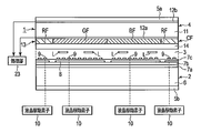
- FIG. 1 and 2 are cross-sectional views showing an example of a liquid crystal panel 1 provided in the liquid crystal display device according to the present embodiment.
- FIG. 1 illustrates a cross section in the horizontal direction of a red pixel RP, a green pixel GP, and a blue pixel BP.
- FIG. 2 illustrates a cross section in the horizontal direction of the green pixel GP.
- the upper side of the liquid crystal panel 1 (hereinafter sometimes referred to as the front side or the display surface side) is the observer side, and the lower side (back side) of the liquid crystal panel 1 is the inner side of the liquid crystal display device. is there.
- the liquid crystal display device includes a light control element (not shown) and a backlight unit (not shown) below the liquid crystal panel 1.
- the liquid crystal panel 1 includes an array substrate 2, a liquid crystal layer 3, and a color filter substrate 4.
- the array substrate 2 and the color filter substrate 4 face each other through the liquid crystal layer 3.
- An alignment film (not shown) is formed at the interface between the array substrate 2 and the liquid crystal layer 3.
- An alignment film (not shown) is formed at the interface between the color filter substrate 4 and the liquid crystal layer 3.
- Optical films 5 a and 5 b are provided on the upper and lower sides of the liquid crystal panel 1.
- the optical films 5a and 5b include a polarizing plate and a retardation plate, or a polarizing plate.
- the optical axes (absorption axes of the polarizing plates) of the two optical films 5a and 5b are crossed Nicols. Thereby, the liquid crystal display device becomes normally black.
- the array substrate 2 includes a transparent substrate 6, insulating layers 7a to 7c, a common electrode 8, a pixel electrode 9, and a liquid crystal driving element (active element) 10.
- a liquid crystal driving element for example, a thin film transistor can be used.
- the transparent substrate 6 for example, a glass plate is used.
- insulating layers 7 a and 7 b are formed on the first plane of the transparent substrate 6, insulating layers 7 a and 7 b are formed.
- a common electrode 8 is formed on the insulating layer 7b.
- An insulating layer 7c is formed on the insulating layer 7b on which the common electrode 8 is formed.
- a pixel electrode 9 is formed on the insulating layer 7c.
- the insulating layers 7a to 7c for example, SiN, SiO2, or a mixture thereof is used.
- the pixel electrode 9 and the common electrode 8 may include a conductive metal oxide.
- the conductive metal oxide for example, a transparent conductive film such as ITO is used.
- the pixel electrode 9 side of the array substrate 2 is the liquid crystal layer 3 side.
- the second plane side of the transparent substrate 6 of the array substrate 2 is the inner side of the liquid crystal display device.
- the common electrode 8, the pixel electrode 9, and the liquid crystal driving element 10 are provided for each pixel.
- the common electrode 8 and the pixel electrode 9 can be, for example, comb-like, band-like, linear, plate-like, or stripe-like patterns.
- the common electrode 8 has a plate-like pattern
- the pixel electrode 9 has a comb-like pattern.
- the cross section of the pixel electrode 9 is a cross section perpendicular to the comb tooth longitudinal direction.
- liquid crystal driving element 10 switches between application and non-application of a liquid crystal driving voltage between the common electrode 8 and the pixel electrode 9.
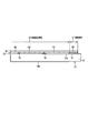
- the horizontal width of the pixel electrode 9 is Wl and the space width (gap) is Ws.
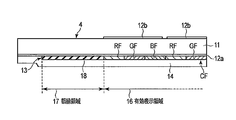
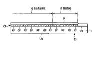
- the color filter substrate 4 includes a transparent substrate 11, transparent electrode layers 12 a and 12 b, a color filter layer 13, and a transparent resin layer 14.
- a transparent substrate 11 for example, glass is used.
- the transparent electrode layer 12 a is formed on the first plane of the transparent substrate 11, and the transparent electrode layer 12 b is formed on the second plane of the transparent substrate 11.
- a color filter layer 13 is formed on the transparent electrode layer 12a.
- the color filter layer 13 includes the color filter CF, but may further include a light shielding layer such as a black matrix.
- the color filter CF includes a red filter RF, a blue filter BF, and a green filter GF.
- a transparent resin layer 14 is formed on the color filter layer 13.
- the transparent resin layer 14 side of the color filter substrate 4 is the liquid crystal layer 3 side.
- the transparent electrode layer 12b side of the color filter substrate 4 is an observer side.
- the display surface is a surface viewed from the viewer side, and is the surface opposite to the transparent resin layer 14 side.
- a transparent electrode layer 12b for touch sensing is formed on the observer-side plane of the transparent substrate 11, and a transparent electrode layer for touch sensing is formed on the plane of the transparent substrate 11 on the liquid crystal layer 3 side. 12a is formed.
- the liquid crystal layer 3 includes, for example, IPS liquid crystal molecules L.
- the dielectric anisotropy of the liquid crystal molecules L is negative, but may be positive.
- the major axis of the liquid crystal molecules L is substantially lateral in plan view when no liquid crystal driving voltage is applied, and the liquid crystal driving voltage is applied as shown in FIG. Thus, it is substantially in the vertical direction in plan view.
- the major axis of the liquid crystal molecules L may be substantially vertical in a plan view when no liquid crystal drive voltage is applied, and may be substantially horizontal in a plan view when a liquid crystal drive voltage is applied. .
- the processing unit 23 detects the capacitance change between the transparent electrode layers 12a and 12b, and detects the position of the pointer or the movement of the pointer.
- the horizontal direction corresponds to a direction in which a plurality of comb teeth of the pixel electrode 9 are arranged or a direction perpendicular to the major axis direction of the comb teeth of the pixel electrode 9.
- liquid crystal molecules L rotate in parallel with the substrate planes of the array substrate 2 and the color filter substrate 4.
- FIG. 3 is a plan view showing an example of the rotation state of the liquid crystal molecules L.
- FIG. FIG. 3 shows a state in which the common electrode 8 is disposed under the pixel electrode 9 in plan view.
- FIG. 3A shows a state in which no liquid crystal driving voltage is applied between the pixel electrode 9 and the common electrode 8.
- FIG. 3B shows a state in which a liquid crystal driving voltage is applied between the pixel electrode 9 and the common electrode 8.
- the liquid crystal molecules L may have a horizontal alignment having a rubbing angle (direction of alignment treatment) ⁇ of about 5 ° to 20 ° with respect to the horizontal direction, for example.
- the liquid crystal molecules L have negative dielectric anisotropy.
- an electric field (electric field) EF1 is generated between the pixel electrode 9 and the common electrode 8.
- the liquid crystal molecules L rotate so that the major axis of the liquid crystal molecules L is perpendicular to the direction of the electric field EF1. As the liquid crystal molecules L rotate, a white display in which light from the backlight unit is transmitted is obtained.
- the change in capacitance when viewed from the substrate vertical direction (thickness direction) is extremely small.
- the change in the dielectric constant of the liquid crystal layer 3 in the thickness direction becomes small, and the accuracy of capacitive touch sensing is not adversely affected.
- the dielectric constant in the thickness direction of the liquid crystal layer 3 may change (the capacitance of the liquid crystal layer 3 changes) by the operation of the liquid crystal molecules L. For this reason, in order to raise the detection accuracy of touch sensing, it is more preferable to use the liquid crystal molecules L which are initial horizontal alignment and are IPS.
- FIG. 4 is a cross-sectional view showing an example of the state of the liquid crystal molecules L having negative dielectric anisotropy when the electric field EF2 in the direction perpendicular to the substrate is generated.
- FIG. 4 shows a cross-sectional view in the lateral direction.
- an electric field EF2 is also formed between the transparent electrode layer 12a and the liquid crystal layer 3 due to the influence of a large capacitance.
- the dielectric anisotropy of the liquid crystal molecules L is negative, the operation of the liquid crystal molecules L is hardly affected by the electric field EF2, and does not greatly affect the quality of the liquid crystal display.
- FIG. 5 is a cross-sectional view showing an example of the state of the liquid crystal molecules L having positive dielectric anisotropy when the electric field EF2 in the direction perpendicular to the substrate is generated.
- FIG. 5 shows a cross-sectional view in the lateral direction.
- the liquid crystal molecules L have positive dielectric anisotropy and the initial alignment is horizontal to the substrate plane.
- an electric field EF2 is formed, and the liquid crystal molecules L rise in a direction along the electric field EF2. This operation may cause light leakage or unintentional coloring in the liquid crystal display.
- the dielectric anisotropy of the liquid crystal molecules L is more preferably negative.
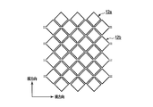
- FIG. 6 is a plan view showing a first example of the transparent electrode layers 12a and 12b according to the present embodiment.
- FIG. 6 shows a state in which the transparent electrode layer 12a is disposed under the transparent electrode layer 12b in plan view. That is, FIGS. 6 and 7 show a state in which the transparent electrode layer 12b and the transparent electrode layer 12a are viewed from the observer side.
- the transparent electrode layer 12b has a pattern in which a plurality of rhombuses are connected in the horizontal direction.
- the transparent electrode layer 12a is a pattern in which a plurality of hexagons are connected in the vertical direction.
- FIG. 7 is a plan view showing a second example of the transparent electrode layers 12a and 12b according to the present embodiment.
- the transparent electrode layer 12b has a pattern in which a plurality of squares are connected in the horizontal direction.
- the transparent electrode layer 12a is a pattern in which a plurality of quadrangles are connected in the vertical direction.
- the transparent electrode layer 12a and the transparent electrode layer 12b are orthogonal to each other in plan view.
- the direction of connection can be freely changed.
- the transparent electrode layers 12a and 12b are alternately arranged in a plan view with substantially no gap.
- a change in capacitance between the transparent electrode layer 12b and the transparent electrode layer 12a closest to the pointer position is detected. Thereby, the position of the pointer or the movement of the pointer can be specified.
- An antireflection film having a refractive index of 1.6 or less may be laminated on the surface of the transparent electrode layer 12b and the surface of the transparent electrode layer 12a.
- FIG. 8 is a plan view showing a third example of the transparent electrode layers 12a and 12b according to the present embodiment.
- the transparent electrode layer 12b is a stripe pattern extending in the horizontal direction.
- the transparent electrode layer 12a is a stripe pattern extending in the vertical direction.
- the transparent electrode layers 12a and 12b are overlapped with no gap in plan view.
- the shape and area of the transparent electrode layer 12b and the transparent electrode layer 12a can be appropriately adjusted.
- the pattern sizes of the transparent electrode layer 12b and the transparent electrode layer 12a can be variously adjusted based on the required resolution or the sizes and pitches of the red filter RF, the green filter GF, and the blue filter BF of the color filter CF.
- the transparent electrode layer 12b and the transparent electrode layer 12a are generated by forming a transparent metal oxide film such as ITO on both surfaces of the transparent substrate 4 and patterning it by a photolithography method.
- the transparent electrode layer 12a and the transparent electrode layer 12b which are detection electrodes for touch sensing, are disposed at positions closer to the pointer. For this reason, the electrostatic capacitance change by a pointer can be detected with high sensitivity.
- the position of the pointer can be detected with high accuracy by the transparent electrode layer 12b connected in the horizontal direction and the transparent electrode layer 12a connected in the vertical direction.
- the touch sensing function can be integrated with the color filter substrate 4, specifically, provided on both surfaces of the transparent substrate 11. Therefore, for example, it is possible to prevent an excessive thickness and weight from increasing as in an on-cell touch panel.
- the transparent electrode layer 12b and the transparent electrode layer 12a are arranged as a pattern having no gap in plan view as much as possible. As a result, the liquid crystal display device can be prevented from being affected by an external electric field from the display surface.
- liquid crystal molecules L having negative dielectric anisotropy are used. In this case, for example, even when the liquid crystal display device receives high-voltage static electricity from the pointer, the liquid crystal molecules L are less likely to move in the thickness direction, and deterioration of the quality of the liquid crystal display can be prevented. .
- liquid crystal display device it is not necessary to provide a shield electrode dedicated for shielding on the color filter substrate 4 side.
- the transparent electrode layer 12b is provided at a position close to the pointer, the sensitivity (capacitance size) of the transparent electrode layer 12b is determined by the capacitance element in the liquid crystal cell. It is better than using the in-cell technology to be arranged. Therefore, in the present embodiment, the position or movement of the pointer can be detected with high accuracy.
- gap between the transparent electrode layer 12b and the transparent electrode layer 12a means that the space
- FIG. 9 is a cross-sectional view showing an example of a conventional color filter substrate 15.
- the conventional color filter substrate 15 of FIG. 9 is provided in an IPS or FFS (fringe field switching) liquid crystal display device.
- the color filter substrate 15 includes, for example, a black matrix BM having a film thickness of about 2 ⁇ m as a light shielding layer for improving the contrast of the liquid crystal display device.
- a red filter RF1, a green filter GF1, and a blue filter BF1 are provided on the black matrix BM.
- the height H of the protrusion may be approximately 1 ⁇ m or more, for example.
- the height H of the protrusion becomes larger as the pixel becomes higher definition, and it becomes difficult to maintain uniform liquid crystal alignment on the surface of the color filter substrate 15.
- the color filter CF and the black matrix BM do not overlap with each other in the thickness direction and no protrusion is formed in the effective display area. Can be flattened.
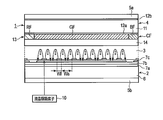
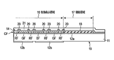
- FIG. 10 is a plan view showing an example of the color filter substrate 4 according to the present embodiment.
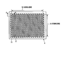
- the display screen includes an effective display area 16 and a frame area 17.
- the frame area 17 surrounds each side of the effective display area 16.
- FIG. 11 is a cross-sectional view showing an example of the color filter substrate 4 according to the present embodiment.
- FIG. 11 shows an A-A ′ cross section of FIG.
- the color filter substrate 4 has a configuration in which transparent electrode layers 12a and 12b are respectively formed on both planes of the transparent substrate 11, and a color filter layer 13 and a transparent resin layer 14 are laminated on the transparent electrode layer 12a.
- FIG. 11 shows the transparent electrode layer 12b on the top and the transparent resin layer 14 on the bottom as in FIG.
- the color filter layer 13 includes a red filter RF, a green filter GF, a blue filter BF, and a light shielding layer 18.
- a color filter CF is formed in the effective display area 16 of the color filter layer 13, and a light shielding layer 18 is formed in the frame area 17.
- the light shielding layer 18 is, for example, a coating film pattern containing carbon as a main material (main component, main agent, or main component) of a visible light shielding color material.
- the main material of the light-shielding color material is a pigment having a mass exceeding 50% with respect to the mass of all pigments of the light-shielding color material in mass ratio.
- the color filter substrate 4 according to this embodiment does not form the black matrix BM in the effective display area 16. Therefore, a high-definition and flat color filter CF can be provided.
- the film thickness of each of the light shielding layer 18 and the red filter RF, the green filter GF, and the blue filter BF may be approximately 2.5 ⁇ m
- the film thickness of the transparent resin layer 14 may be approximately 2 ⁇ m
- the total film thickness of the color filter CF and the transparent resin layer 14 is preferably in the range of approximately 2.5 ⁇ m to 9 ⁇ m, or approximately 2.5 ⁇ m to 4.5 ⁇ m.
- the change in electric capacity when the liquid crystal layer 3 is viewed from the thickness direction is extremely small.
- equipotential lines from the pixel electrode 9 to which a driving voltage is applied have a uniform spread from the pixel electrode 9 in the thickness direction of the liquid crystal layer 3 as much as possible. It is preferable. If the equipotential lines are distorted or if the density of the equipotential lines is different for each color of the color filter, light leakage or unintentional coloring of the pixels occurs.
- a transparent electrode such as VcomITO is provided on the color filter, which may reduce the transmittance of the liquid crystal display device.
- the transparent electrode layer (or shield layer) 12 a is provided as a conductive film at a position close to the liquid crystal layer 3, the equipotential lines are flat in the thickness direction of the liquid crystal layer 3. Become a shape. In this case, the liquid crystal molecules L that operate in the liquid crystal layer 3 are very small in the thickness direction, and the transmittance of the liquid crystal display device may be reduced, resulting in dark display.
- the total film thickness of the color filter CF and the transparent resin layer 14 provided under the transparent electrode layer 12a in FIG. 13 is preferably thicker, for example, equal to or greater than the thickness of the liquid crystal layer 3. Preferably there is.
- the equipotential lines can be spread uniformly in the liquid crystal layer 3. it can.
- the total film thickness of the transparent resin layer 14 and the color filter CF is, for example, about 2.5 ⁇ m to avoid the equipotential lines from becoming flat in the thickness direction of the liquid crystal layer 3. It is good also as a range of 9 micrometers. In this way, by setting the total film thickness of the transparent resin layer 14 and the color filter CF to a range that is approximately twice the thickness of the liquid crystal layer 5 from the thickness of the liquid crystal layer 5, as shown in FIG. The spread of equipotential lines from the electrode 9 can be expanded in the direction of the color filter CF.
- the red filter RF, the green filter GF, and the blue filter BF are approximately 2.9 or more when measured at the frequency for driving the liquid crystal, have a relative dielectric constant of 4.4 or less, and The relative dielectric constants of the red filter RF, the green filter GF, and the blue filter BF are assumed to be within a range of about ⁇ 0.3 with respect to the average relative dielectric constants of the red filter RF, the green filter GF, and the blue filter BF. Also good.
- the relative dielectric constants of the red filter RF, the green filter GF, and the blue filter BF are within a range of about ⁇ 0.3 (the difference is less than the average relative dielectric constant of the red filter RF, the green filter GF, and the blue filter BF). 0.3 or less). By setting the difference in relative permittivity within this range, color unevenness can be prevented.
- the relative dielectric constant of the color filter CF is lowered by increasing the ratio of the transparent resin serving as a dispersion matrix (matrix) of the organic pigment. Can be made.
- the relative dielectric constants of the red filter RF, the green filter GF, and the blue filter BF can be suppressed to a small range within the appropriate film thickness range as described above.
- the display quality for each of the filter GF and the blue filter BF can be matched.
- the relative dielectric constant of the color filter CF is measured at a frequency of approximately 120, 240, and 480 Hz under the condition of a voltage of 5 V using an impedance analyzer.
- a color filter CF is applied and hardened on a glass substrate on which a conductive film made of an aluminum thin film is patterned (the film thickness is the same as in the embodiments described later), and an aluminum thin film is formed on the color filter CF. It is produced
- the minimum thickness (cell thickness) of the liquid crystal layer 3 that can ensure the yield in the cell forming step is about 2.5 ⁇ m.
- the upper limit of the thickness of the liquid crystal layer 3 that is a liquid crystal material having a small ⁇ n and is easy to drive the liquid crystal is, for example, about 4.5 ⁇ m.
- a more preferable thickness of the liquid crystal layer 3 is, for example, approximately 2.5 ⁇ m to 4.5 ⁇ m.
- the total film thickness of the color filter CF and the transparent resin layer 14 ranges from a thin film thickness of about 2.5 ⁇ m at a practical level of the liquid crystal layer 3 to a thick film thickness at a practical level of the liquid crystal layer 3 of 4.5 ⁇ m.
- FIG. 14 is a cross-sectional view showing an example of the relationship between the horizontal width Wl and pitch Ws of the pixel electrodes and the lines of electric force.
- FIG. 14 is a cross-sectional view in the lateral direction.
- a pixel electrode 9 and a common electrode 8 for driving liquid crystal are formed on the array substrate 2 side.
- the display of each pixel can be homogenized.
- the matched three-color display can be realized as the relative dielectric constants (electrical characteristics) of the red filter RF, the green filter GF, and the blue filter BF match.
- the relative permittivity of the light shielding layer 18 is also preferably close to the relative permittivity of each of the red filter RF, the green filter GF, and the blue filter BF.
- the transparent resin layer 14 and the color filter CF are applied with different microscopic potentials.
- the way of equipotential lines entering the transparent resin layer 14 and the color filter CF is not microscopically uniform. Therefore, when a liquid crystal driving voltage is applied to the liquid crystal layer 3, unevenness of accumulated charges occurs on the surface of the transparent resin layer 14 that is an insulator. The accumulated charge unevenness generates an offset voltage on the surface of the transparent resin layer 14 and causes microscopic liquid crystal display unevenness or display burn-in.
- the transparent electrode layer 12a has such an effect as a secondary effect.
- the liquid crystal molecules in the liquid crystal layer 3 do not stand up even when an alternating current is applied to the transparent electrode layer 12a. Does not drop.
- the light shielding layer 18 is a coating film pattern containing carbon as a main material of the visible light shielding color material.
- the light shielding layer 18 containing carbon has a high relative dielectric constant.
- the image quality can be improved by increasing the thickness of each of the red filter RF, the green filter GF, and the blue filter BF and increasing the thickness of the transparent resin layer 14. it can. That is, it is possible to prevent the equipotential lines from being distorted, the light leakage, and the dark part.
- the refractive index anisotropy ⁇ n at a wavelength of 550 nm is about 0.1
- the dielectric constant in the direction parallel to the alignment vector of the liquid crystal is about 4.1
- the dielectric anisotropy ⁇ is a negative liquid crystal of approximately -6.1.
- the thickness of the liquid crystal layer 3 may be approximately 3.5 ⁇ m.
- FIG. 15 is a cross-sectional view showing an example of the color filter substrate 19 according to the present embodiment.
- the color filter substrate 19 has transparent electrode layers 12a and 12b formed on both planes of the transparent substrate 11, respectively.
- the color filter layer 13, the transparent resin layer 14, the light shielding layer 20, and the transparent resin layer are formed on the transparent electrode layer 12a. 21 is laminated.
- FIG. 15 shows that the film surface (surface of the color filter CF) is opposite to that in FIG. 11, that is, the transparent electrode layer 12b is down and the transparent resin layer 21 is up.
- the main difference between the color filter substrate 4 according to the first embodiment and the color filter substrate 19 according to the present embodiment is that a light shielding layer 20 is formed in the effective display area 16.
- the light shielding layer 20 is formed on each of a part of the red filter RF, a part of the green filter GF, and a part of the blue filter BF.
- the light shielding layer 20 may be provided at each boundary portion of the red filter RF, the green filter GF, and the blue filter BF, and may separate the red filter RF, the green filter GF, and the blue filter BF.
- the light shielding layer 20 may be provided as a black matrix.
- the light shielding layer 20 is a coating film pattern containing an organic pigment as a main material of a visible light shielding color material.
- the relative dielectric constant of the light shielding layer 20 is smaller than the relative dielectric constant of the light shielding layer 18 containing carbon as a main material of the visible light shielding color material.
- the relative permittivity of the light shielding layer 20 can be made equal to the relative permittivity of each of the red filter RF, the green filter GF, and the blue filter BF.
- the light shielding layer 20 containing an organic pigment as the main material of the visible light shielding color material is provided at a position close to the liquid crystal layer 3, the equipotential lines from the pixel electrodes 9 are not distorted, and the light shielding layer 20 Light leakage in the vicinity can be prevented.
- a liquid crystal in which a liquid crystal layer 3 having an initial orientation horizontal to the substrate plane of the array substrate 2 and including liquid crystal molecules L rotating in parallel with the substrate plane when a liquid crystal driving voltage is applied to the plurality of pixel electrodes 9 is used.
- the light shielding layer 20 can be disposed at a position close to the thickness direction from the liquid crystal layer 3.
- the coating film layer 20 containing an organic pigment as the main material of the visible light-shielding colorant at a position close to the liquid crystal layer 3, adjacent pixels that are peculiar to IPS or FFS liquid crystal driving Light leakage and inappropriate coloring can be suppressed.
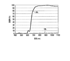
- FIG. 16 is a graph showing an example of the transmittance characteristic 18L of the light shielding layer 18 and the transmittance characteristic 20L of the light shielding layer 20.
- the transmittance characteristic 20L of the light shielding layer 20 illustrates the transmittance characteristic in which a plurality of organic pigments are mixed and dispersed.
- the light-shielding layer 20 containing an organic pigment as a main light-shielding colorant has a transmittance characteristic 20L that transmits light having a wavelength longer than about 680 nm or 780 nm, for example. Therefore, the light shielding layer 20 has the characteristics of an infrared transmission filter.
- the light-shielding layer 18 containing carbon as a main light-shielding colorant has a characteristic 18L that shields light at a wavelength in the visible light region and shields light even at longer wavelengths than the visible light region including the infrared region.
- the wavelength at which the transmittance characteristic 20L of the light shielding layer 20 rises and becomes a half value may be set in a range of approximately 670 nm to 750 nm by selecting or mixing organic pigment species.
- FIG. 17 is a graph showing an example of transmittance characteristics of the color filter CF according to the present embodiment.
- the color filter CF includes a red filter RF, a green filter GF, and a blue filter BF.
- a characteristic RL is a transmittance characteristic of the red filter RF.
- the characteristic GL is a transmittance characteristic of the green filter GL.
- a characteristic BL is a transmittance characteristic of the blue filter BF.
- the transmittances of the red filter RF, the green filter GF, and the blue filter BF are greatly different at longer wavelengths than the light wavelength of about 700 nm.
- liquid crystal display device including an optical sensor is used as a color copy device or an imaging device, for example, in a near-infrared wavelength range of about 700 nm to 1100 nm, a highly accurate red, green, Blue color separation is difficult.
- the photodiode can detect light in a wavelength range of approximately 400 nm to 1100 nm.
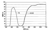
- FIG. 18 is a graph showing an example of the transmittance characteristic GL of the green filter GF and the transmittance characteristic GLBLK in which the green filter GF and the light shielding layer 20 are optically overlapped.
- a portion in which the single color layers of the red filter RF, the blue filter BF, and the green filter GF included in the color filter CF and the light shielding layer 20 are overlapped to detect light may be referred to as an optical overlapping portion.
- High-precision green detection data in the visible light range is obtained by subtracting light detection data detected by optically overlapping the green filter GF and the light shielding layer 20 from light detection data detected via the green filter GF. Is obtained.
- the green light in the visible light region is subtracted. Only the detected data can be extracted.
- FIG. 19 is a graph showing an example of the transmittance characteristic RL of the red filter RF and the transmittance characteristic RLBLK in which the red filter RF and the light shielding layer 20 are optically overlapped.
- the high-precision red detection data in the visible light range is obtained by subtracting the detection data of the light detected by optically overlapping the red filter RF and the light shielding layer 20 from the detection data of the light detected via the red filter RF. Is obtained.
- red in the visible light range is obtained. Only the detected data can be extracted.
- FIG. 20 is a graph showing an example of the transmittance characteristic BL of the blue filter BF and the transmittance characteristic BLBLK in which the blue filter BF and the light shielding layer 20 are optically overlapped.
- the high-precision blue detection data in the visible light range is obtained by subtracting the detection data of the light detected by optically overlapping the blue filter BF and the light shielding layer 20 from the detection data of the light detected via the blue filter BF. Is obtained.
- FIG. 21 is a cross-sectional view showing an example of the plurality of optical sensors 22a and 22b and the processing unit 23.
- the optical sensor 22a generates detection data of the light 24a via the green filter GF.
- the optical sensor 22 b generates detection data of the light 24 b that passes through the green filter GF and the light shielding layer 20.
- the detection data of the optical sensor 22a includes a green photosensitive component and a near-infrared photosensitive component.
- the processing unit 23 can extract the detection data of only the green component in the visible light region by subtracting the detection data of the optical sensor 22b from the detection data of the optical sensor 22a.
- the green filter GF with the red filter RF or the blue filter BF, it is possible to extract the detection data of the red component or the blue component in the visible light region, respectively.
- the light shielding layer 20 is disposed at a position close to the liquid crystal layer 3 except for the transparent resin layer 21 and an alignment film (not shown) among the components of the color filter substrate 19.
- the position of the light shielding layer 20 can obtain an effect of suppressing color mixture from adjacent pixels in an IPS liquid crystal display device having a long liquid crystal operation propagation distance in the lateral direction parallel to the substrate plane.
- the light shielding layer 20 has an effect of suppressing light leakage due to crosstalk when driving adjacent pixels.
- the plurality of pixels may include pixels having a width in the horizontal direction (hereinafter referred to as a horizontal width) that is 1 ⁇ 2 compared to other pixels.
- a pixel having a width of 1/2 has a shape that is long in the vertical direction.
- the plurality of pixels may include a pixel having a vertical width (hereinafter, referred to as a vertical width) of 1 ⁇ 2 compared to other pixels, instead of a shape that is long in the vertical direction.
- a pixel having a vertical width of 1 ⁇ 2 has a shape that is long in the horizontal direction.
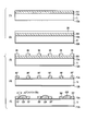
- FIG. 22 is a cross-sectional view showing an example of the color filter substrate 25 according to this embodiment.
- the color filter substrate 25 includes color filters CF in both the effective display area 16 and the frame area 17. Therefore, the process of forming the light shielding film 18 in the frame region 17 can be eliminated, and the manufacturing method can be made more efficient.
- the color filter substrate 25 has a horizontal width of the first formed red filter RF that is approximately 1 ⁇ 2 of the horizontal width of the other green filters GF and blue filters BF. .
- the frame region 17 of the color filter substrate 25 may be formed by a dummy turn.
- the red filter RF is provided between the green filter GF and the blue filter BF in a plan view, and separates the green filter GF and the blue filter BF.
- FIG. 23A and FIG. 23B show an example of a cross-sectional view of each intermediate product in the process related to the method for manufacturing the color filter substrate 25 according to the present embodiment.
- the color filter substrate 25 manufacturing apparatus includes, for example, a coating apparatus, a dryer, an exposure apparatus, a developing apparatus, a film forming apparatus, and a sputtering apparatus.
- a typical dryer and film hardening apparatus a clean oven, a hot plate, or the like is used.
- the first color filter is formed by a dry etching method, but the first color filter may be formed by a known photolithography method.
- transparent electrode layers 12a and 12b are formed on both surfaces of the transparent substrate 11, and a red resist (red photosensitive coloring composition) RR is formed on the transparent electrode layer 12a. It is formed.
- the red resist RR is applied to the entire surface of the transparent substrate 11 so that the coating thickness after drying becomes approximately 2.5 ⁇ m, and is dried and hardened.
- a positive photosensitive resist layer 26 is formed on the red resist RR.
- the positive photosensitive resist layer 26 is formed into a linear pattern.
- This linear pattern is the same as the linear pattern of the red filter RF.
- the linear pattern or the alignment mark is formed by, for example, a well-known photolithography method.
- a cross-shaped alignment mark is formed on the edge of the substrate using, for example, a red resist RR.
- the red resist RR is dry-etched together with the linear pattern of the positive photosensitive resist layer 26.
- a red filter RF having a linear pattern is formed.
- the linear pattern of the positive photosensitive resist layer 26 is removed during etching. However, a part of the linear pattern of the photosensitive resist layer 26 may be left, or the linear pattern of the photosensitive resist layer 26 may be removed with a stripping solution.
- the end point of etching can be determined by detecting the transparent electrode layer 12a.
- anisotropic etching for etching in the vertical direction.
- the cross-sectional shape of the red filter RF can be controlled by the composition of the gas introduced into the etching apparatus, the etching rate, or the magnetic field conditions.
- a green resist GR is formed on the substrate to be processed.
- the green resist GR is applied so that the film thickness after drying is approximately 2.5 ⁇ m.
- the substrate is aligned using alignment marks, exposed by an exposure device, developed by a developing device, and a green filter is interposed between two red filters RF as shown in (6) of FIG. 23B. GF is formed.
- the green resist GR is imparted with heat flow properties (fluidization by heat treatment) and the green filter GF is formed from the green resist GR by heat treatment hardening.
- the positional deviation ⁇ which is an alignment error
- the development and hardening process for forming the green filter GF is the same as the formation of the red filter RF.
- a blue resist BR is formed on the substrate to be processed.
- the blue resist BR is applied so that the film thickness after drying is approximately 2.5 ⁇ m.
- the substrate is dried by a drier, aligned using alignment marks, exposed by an exposure device, developed by a developing device, and two red filters as shown in FIG. 23B (8).
- a blue filter BF is formed between RF.
- the red pigment contained in the red resist RR and the red filter RF is different from the green pigment and the blue pigment represented by the halogenated phthalocyanine pigment, and the halogen and metal (central metal of the pigment structure) contained in the pigment structure. Less suitable for dry etching. In other words, in the red pigment, it is easy to suppress contamination by halogen or metal during dry etching.
- the blue resist BR blue coloring composition
- the formation of the blue filter BF is performed in the order of forming the filters of a plurality of colors as described above. It is preferable that it is the second or later.
- the line width of at least one of the red filter RF and the green filter GF is set to 1 ⁇ 2 of the line width of the blue filter BF.
- the 1/2 line width filter may be divided and arranged. Since blue is a color with low visibility, it is desirable to avoid dividing the line width into 1 ⁇ 2 widths.
- FIG. 24 is a cross-sectional view showing an example of the color filter substrate 27 according to the present embodiment.
- a light shielding layer 18 having a thickness of about 1 ⁇ m is formed as a black matrix on the transparent electrode layer 12a.
- a red filter RF, a green filter GF, and a blue filter BF each having a thickness of about 3 ⁇ m are formed.
- a light shielding layer 18 having a thickness of about 1 ⁇ m is formed on the transparent electrode layer 12a.
- a light shielding layer 20 having a thickness of about 2 ⁇ m is formed on the transparent electrode layer 12a on which the light shielding layer 18 is formed.
- the light shielding layer 18 in the effective display area 16 and the light shielding layer 18 in the frame area 17 are formed by the same process and the same material.
- the thicknesses of the red filter RF, green filter GF, and blue filter BF in the effective display area 16 and the light shielding layers 18 and 20 in the frame area 17 are substantially the same, and flatness is maintained.
- the transparent resin layer 14 is formed with a thickness of about 2 ⁇ m on the red filter RF, the green filter GF, and the blue filter BF in the effective display area 16 and the light shielding layers 18 and 20 in the frame area 17.
- the color filter CF includes a red filter RF, a green filter GF, a blue filter BF, and a light shielding layer 18 in the effective display area 16.
- the thickness of the light shielding layer 18 in the effective display area 16 is, for example, less than about 1.5 ⁇ m in order to maintain the flatness of the color filter CF.
- the light shielding layer 20 containing an organic pigment as a main light shielding color material may be formed at any position of the red filter RF, the green filter GF, and the blue filter BF in the effective display area 16.
- the manufacturing method of the color filter substrate 4 will be described as a representative, but the same manufacturing method can be applied to the other color filter substrates 19, 25, and 27.
- the photosensitive coloring composition used for forming the color filters CF such as the light shielding layers 18 and 20, the red filter RF, the green filter GF, and the blue filter BF is a polyfunctional monomer, photosensitivity in addition to the pigment dispersion (hereinafter referred to as paste).
- Resin or non-photosensitive resin, polymerization initiator, solvent and the like are contained.
- highly transparent organic resins such as photosensitive resins and non-photosensitive resins used in this embodiment are collectively referred to as transparent resins.
- thermoplastic resin examples include butyral resin, styrene-maleic acid copolymer, chlorinated polyethylene, chlorinated polypropylene, polyvinyl chloride, vinyl chloride-vinyl acetate copolymer, polyvinyl acetate, polyurethane resin, and polyester resin.
- Acrylic resins, alkyd resins, polystyrene resins, polyamide resins, rubber resins, cyclized rubber resins, celluloses, polybutadiene, polyethylene, polypropylene, polyimide resins, and the like can be used.
- thermosetting resin for example, epoxy resin, benzoguanamine resin, rosin-modified maleic acid resin, rosin-modified fumaric acid resin, melamine resin, urea resin, phenol resin and the like can be used.
- the thermosetting resin may be generated by reacting a melamine resin and a compound containing an isocyanate group.
- ⁇ Alkali-soluble resin> In forming the light shielding films such as the light shielding layers 18 and 20, the transparent resin layers 9, 9a and 9b, and the color filter CF according to the present embodiment, it is preferable to use a photosensitive resin composition capable of forming a pattern by photolithography. .
- These transparent resins are desirably resins imparted with alkali solubility.
- the alkali-soluble resin a resin containing a carboxyl group or a hydroxyl group may be used, or another resin may be used.
- alkali-soluble resin examples include epoxy acrylate resins, novolac resins, polyvinyl phenol resins, acrylic resins, carboxyl group-containing epoxy resins, and carboxyl group-containing urethane resins.
- the alkali-soluble resin it is preferable to use an epoxy acrylate resin, a novolac resin, or an acrylic resin, and an epoxy acrylate resin or a novolac resin is particularly preferable.
- red pigments include C.I. I. Pigment Red 7, 9, 14, 41, 48: 1, 48: 2, 48: 3, 48: 4, 81: 1, 81: 2, 81: 3, 97, 122, 123, 146, 149, 168, 177, 178, 179, 180, 184, 185, 187, 192, 200, 202, 208, 210, 215, 216, 217, 220, 223, 224, 226, 227, 228, 240, 242, 246, 254, 255, 264, 272, 279, or the like can be used.
- yellow pigments examples include C.I. I. Pigment Yellow 1, 2, 3, 4, 5, 6, 10, 12, 13, 14, 15, 16, 17, 18, 20, 24, 31, 32, 34, 35, 35: 1, 36, 36: 1, 37, 37: 1, 40, 42, 43, 53, 55, 60, 61, 62, 63, 65, 73, 74, 77, 81, 83, 86, 93, 94, 95, 97, 98, 100, 101, 104, 106, 108, 109, 110, 113, 114, 115, 116, 117, 118, 119, 120, 123, 125, 126, 127, 128, 129, 137, 138, 139, 144, 146, 147, 148, 150, 151, 152, 153, 154, 155, 156, 161, 162, 164, 166, 167, 168, 169, 170, 171, 172, 1 73, 174, 175, 176, 177, 179, 180, 181, 18
- blue pigments examples include C.I. I. Pigment Blue 15, 15: 1, 15: 2, 15: 3, 15: 4, 15: 6, 16, 22, 60, 64, 80, etc., among which C.I. I. Pigment Blue 15: 6 is preferred.
- purple pigments examples include C.I. I. Pigment Violet 1, 19, 23, 27, 29, 30, 32, 37, 40, 42, 50 and the like can be used. I. Pigment Violet 23 is preferred.
- green pigments examples include C.I. I. Pigment Green 1, 4, 4, 7, 8, 10, 13, 14, 15, 17, 18, 19, 26, 36, 45, 48, 50, 51, 54, 55, 58, etc. can be used.
- C.I. is a halogenated zinc phthalocyanine green pigment.
- I. Pigment Green 58 is preferred.
- As the green pigment a halogenated aluminum phthalocyanine pigment may be used.
- the light-shielding color material contained in the light-shielding layers 18 and 20 is a color material having an absorptivity in the visible light wavelength region and having a light-shielding function.
- an organic pigment, an inorganic pigment, or a dye can be used as the light-shielding color material.
- inorganic pigments include carbon black and titanium oxide.
- the dye that can be used include azo dyes, anthraquinone dyes, phthalocyanine dyes, quinoneimine dyes, quinoline dyes, nitro dyes, carbonyl dyes, and methine dyes.
- the organic pigment for example, the above organic pigment may be applied.
- 1 type may be used for a light-shielding component and it may combine 2 or more types by a suitable ratio.
- Example of black resist 1 applied to light shielding layer 18 A preparation example of a black paste (dispersion) used for the light shielding layer 18 containing carbon as the main material of the light shielding color material will be described.
- a mixture having the following composition is stirred and mixed uniformly, and stirred with a bead mill disperser to produce a black paste.
- Each composition is expressed in parts by mass.
- the black resist 1 filtered and applied to the light shielding layer 18 is prepared.
- the resist refers to a photosensitive coloring composition containing carbon or an organic pigment.
- the main color material (pigment) in the black resist 1 or the color resist exceeds 50% with respect to the total mass ratio (%) of the color material (pigment) contained in the resist.
- carbon accounts for 100% of the color material, and carbon is the main color material.
- an organic pigment such as red, yellow, or blue is added in order to adjust the color tone or reflection color, with a total mass ratio of 10% or less. Also good.
- Example of black resist 2 used for light shielding layer 20 An example of a mixture of organic pigments used in the light shielding layer 20 containing an organic pigment as the main material of the light shielding color material is shown below.
- R254 C. I. Pigment Red 254 (hereinafter abbreviated as R254) C. I. Pigment Yellow 139 (hereinafter abbreviated as Y139) C. I. Pigment Violet 23 (hereinafter abbreviated as V23)
- R254 pigment may be excluded.
- a small amount of other types of pigments for adjusting the color (transmission wavelength) for example, the above organic pigments may be added in a small amount of 20% or less.
- a small amount of a halogenated zinc phthalocyanine or aluminum halide phthalocyanine green pigment may be used in order to adjust the rising of the transmittance characteristic in the light shielding layer 20 near the light wavelength of 700 nm (adjustment of the spectral curve shape). .
- the light shielding layer 20 can be provided with the optimum infrared transmittance.
- the light shielding layer 20 desirably has a transmittance in the visible range of 5% or less.
- the visible range is usually approximately the light wavelength 400 nm to 700 nm.
- the half-value wavelength of the light shielding layer 20 in the light wavelength range of 670 nm to 750 nm, it is necessary that the infrared transmittance characteristic rises from around the light wavelength of 660 nm and the transmittance characteristic becomes higher on the long wavelength side.
- the wavelength range of the low transmittance of the light shielding layer 20 may be approximately the light wavelength range of 400 nm to 650 nm.
- the transmittance of the light shielding layer 20 increases the amount of pigment contained in the light shielding layer 20 or increases the film thickness of the light shielding layer 20. It can be realized very easily by increasing the thickness.
- the wavelength position of the half-value wavelength can be easily adjusted based on the amount of the pigment, the composition ratio of a violet pigment, a green pigment, a yellow pigment, and a red pigment, which will be described later, and the film thickness of the light shielding layer 20. .
- the green pigment applied to the light shielding layer 20 various green pigments described later can be applied.
- a green pigment whose light or near-infrared transmittance rises (for example, half-value wavelength) is in the wavelength range of 700 nm to 800 nm. Is preferred. Adjustment for setting the half-value wavelength to the light wavelength range of 670 nm to 750 nm is realized mainly based on the purple pigment and the green pigment. In order to adjust the transmittance characteristic of the light shielding layer 20, a blue pigment may be added.
- the mass ratio (%) of R254 may belong to the range of 0 to 20%, for example.
- the mass ratio (%) of Y139 may belong to a range of 20 to 50%, for example.
- the mass ratio (%) of V23 may belong to the range of 40 to 75%, for example.
- the pigment is dispersed in a resin or a solution to produce a pigment paste (dispersion).
- a resin or a solution for example, in order to disperse the pigment Y139 alone in a resin or solution, the following materials are mixed with 7 parts (mass part) of the pigment R139.
- Acrylic resin solution (solid content 20%) 40 parts Dispersant 0.5 parts Cyclohexanone 23.0 parts
- other pigments such as V23, R254, etc. are also dispersed in the same resin or solution, and a black pigment dispersion paste May be generated.
- composition ratio for producing a black resist based on the above pigment dispersion paste will be exemplified.
- the black resist 2 used for the light shielding layer 20 is formed according to the composition ratio.
- the black resist 2 used for forming the light shielding layer 20 and containing an organic pigment as the main material of the light shielding color material may be added with carbon as a guide at 40% or less of the total mass in order to adjust the light shielding properties.
- a mixture having the following composition is stirred and mixed uniformly, dispersed in a sand mill for 5 hours using glass beads having a diameter of about 1 mm, and filtered through a filter of about 5 ⁇ m to produce a red paste 1.
- Red pigment C.I. I. Pigment Red254 8 parts Red Pigment C.I. I. Pigment Red177 10 parts Yellow Pigment C.I. I. Pigment Yellow 150 2 parts Dispersant 2 parts Acrylic varnish (solid content 20% by mass) 108 parts ⁇ Preparation of red resist RR1>
- a mixture having the following composition is stirred and mixed so as to be uniform and filtered through a filter of about 5 ⁇ m to prepare a red resist RR1.
- Red paste 1 42 parts Acrylic resin solution 18 parts Dipentaerythritol penta and hexaacrylate 4.5 parts Photopolymerization initiator 1.2 parts Sensitizer 2.0 parts Cyclohexanone 32.3 parts ⁇ Color filter substrate 4, 19, 25 , 27 example of red resist RR2> ⁇ Preparation of red paste 2> A preparation example of the red paste 2 (dispersion) will be described below.
- the red paste 2 is produced in the same manner as the red paste 1 using a mixture having the following composition.
- a red resist RR2 is prepared by using the red paste 2 instead of the red paste 1 and the same method as the red resist RR1.
- Green pigment C.I. I. Pigment Green 58 10.4 parts Yellow Pigment C.I. I. Pigment Yellow 150 9.6 parts Dispersant 2 parts Acrylic varnish (solid content 20% by mass) 66 parts ⁇ Preparation of green resist GR1> After the green paste 1 is prepared, a mixture having the following composition is stirred and mixed so as to be uniform and filtered through a filter of approximately 5 ⁇ m to prepare a green resist GR1.
- Green paste 1 46 parts Acrylic resin solution 8 parts Dipentaerythritol penta and hexaacrylate 4 parts Photopolymerization initiator 1.2 parts Photopolymerization initiator 3.5 parts Sensitizer 1.5 parts Cyclohexanone 5.8 parts Propylene glycol monomethyl 30 parts of ether acetate
- the green resist GR may be used by adding 0.08 part of a fluorosurfactant.
- the green paste 2 is produced in the same manner as the green paste 1 using a mixture having the following composition.
- Green pigment C.I. I. Pigment Green 58 10.4 parts Yellow Pigment C.I. I. Pigment Yellow 150 3.2 parts Yellow Pigment C.I. I. Pigment Yellow 138 7.4 parts Dispersant 2 parts Acrylic varnish (solid content 20% by mass) 66 parts ⁇ Preparation of Green Resist GR2>
- a green resist GR2 is prepared by using the green paste 2 in place of the green paste 1 and the same method as the green resist GR1.
- Blue pigment C.I. I. Pigment Blue 15 6 52 parts Dispersant 6 parts Acrylic varnish (solid content 20% by mass) 200 parts ⁇ Preparation of blue resist BR1> After the blue paste 1 is prepared, the mixture having the following composition is stirred and mixed so as to be uniform, and filtered with a filter of about 5 ⁇ m to prepare a blue resist BR1.
- Blue paste 1 16.5 parts Acrylic resin solution 25.3 parts Dipentaerythritol penta- and hexaacrylate 1.8 parts Photopolymerization initiator 1.2 parts Sensitizer 0.2 parts Cyclohexanone 25 parts Propylene glycol monomethyl ether acetate 30 parts ⁇ Example of Blue Resist BR2 Used for Color Filter Substrate 4, 19, 25, 27> ⁇ Preparation of blue paste 2> A mixture of the following composition is dispersed in a mill for 5 hours and filtered through an approximately 5 ⁇ m filter to produce an intermediate blue paste (dispersion).
- Blue dye 2.6 parts ⁇ Preparation of blue resist BR2> A blue resist BR2 is prepared by using the blue paste 2 in place of the blue paste 1 and the same method as the blue resist BR1.
- Table 1 shows an example of the relationship between the relative permittivity of the red resists RR1 and RR2, the green resists GR1 and GR2, and the blue resists BR1 and BR2 and the measurement frequency.
- transparent electrode layers 12a and 12b are formed on both surfaces of the transparent substrate 11 prior to the coloring process of the color filter CF.
- transparent and conductive composite metal oxide such as ITO is used.
- the transparent electrode layers 12a and 12b are formed on the both sides of the transparent substrate 11 by a sputtering apparatus or in two steps for each side.
- the transparent electrode layers 12a and 12b are patterned by a photolithography method.
- the transparent electrode layer 12b may be formed first, and then the transparent electrode layer 12a may be formed.
- the transparent electrode layers 12a and 12b are formed, for example, by performing ITO film formation of the transparent electrode layer 12b on the first plane of the transparent substrate 11, and subsequently photolithography (etching) of the transparent electrode layer 12b. And the resist stripping step), and after this transparent electrode layer 12b forming step, ITO film formation of the transparent electrode layer 12a is performed on the second plane of the transparent substrate 11, and the transparent electrode layer 12a Photolithography (including etching and resist stripping steps) may be performed. At least one pattern of the transparent electrode layers 12a and 12b includes an alignment mark used in the next step.
- the first color (for example, red) alignment mark is aligned with at least one alignment mark of the transparent electrode layers 12 a and 12 b. Generated.
- the black resist 1 containing carbon is applied to the surface on which the transparent electrode layer 12a is formed so as to cover the transparent electrode layer 12a. Dried. Using a photomask including the pattern of the frame region 17 and the pattern of the alignment mark, the black resist 1 is exposed, developed, heated, and hardened to generate the light shielding layer 18 and the alignment mark in the frame region 17. The The alignment of the pattern in the frame region 17 is performed based on this image obtained by photographing the back surface (the direction of the surface on which the transparent electrode layer 12b is formed) coated with the black resist 1 with a camera.
- the black resist 1 is applied to the entire surface of the transparent electrode layer 12a so that the film thickness after drying is approximately 2.5 ⁇ m.
- the substrate to be processed is pre-baked in a clean oven, for example, at 70 ° C. for 20 minutes and cooled at room temperature.
- alignment is performed as a pre-process for exposing to ultraviolet rays.
- a halogen lamp is used as a light source.
- the light from the halogen lamp is irradiated only to the peripheral part of the alignment mark of the transparent electrode layer 12a from the surface side where the transparent electrode layer 12b is formed, and is photographed with a camera.
- the alignment is executed based on the photographing result of this camera. For irradiation only to the periphery of the alignment mark, light whose exposure wavelength is cut by a cut filter is used.
- the coating film surface of the black resist 1 is exposed to ultraviolet rays using an ultra high pressure mercury lamp.
- the photomask used for this exposure includes a frame area 17 pattern and a plurality of cross-shaped alignment mark patterns.
- the pattern of the frame region 17 and the pattern of the alignment mark are exposed with ultraviolet rays.
- the substrate to be processed is washed with spray and ion-exchanged water using a sodium carbonate aqueous solution at 23 ° C. and dried. . After drying, the substrate to be processed is hardened at 230 ° C. for 20 minutes. Thereby, the light shielding layer 18 and the alignment mark in the frame region 17 are formed.
- a red filter RF, a green filter GF, and a blue filter BF are formed by photolithography using the above three color resists sequentially.
- the red resist RR is applied to the substrate to be processed so as to have a film thickness of, for example, 2.5 ⁇ m, dried, and exposed by an exposure machine. And developed to form a striped red filter RF.
- the steps of development and hardening are the same as the formation of the light shielding layer 18 in the frame region 17 described above.
- a green resist GR is applied to a substrate to be processed so as to have a film thickness of 2.5 ⁇ m, for example, dried, exposed by an exposure machine, and developed to form a striped green filter GF. .
- the blue resist BR is applied to a substrate to be processed so as to have a film thickness of, for example, 2.5 ⁇ m, dried, exposed by an exposure machine, and developed to form a striped blue resist BR. .
- the transparent resin layer 14 is formed with a film thickness of about 2 ⁇ m, and the color filter substrate 4 is manufactured.
Landscapes
- Physics & Mathematics (AREA)
- Engineering & Computer Science (AREA)
- General Physics & Mathematics (AREA)
- Nonlinear Science (AREA)
- General Engineering & Computer Science (AREA)
- Theoretical Computer Science (AREA)
- Optics & Photonics (AREA)
- Crystallography & Structural Chemistry (AREA)
- Chemical & Material Sciences (AREA)
- Human Computer Interaction (AREA)
- Mathematical Physics (AREA)
- Liquid Crystal (AREA)
- Geometry (AREA)
- Devices For Indicating Variable Information By Combining Individual Elements (AREA)
- Position Input By Displaying (AREA)
- Optical Filters (AREA)
Abstract
実施形態に係る液晶表示装置は、アレイ基板2とカラーフィルタ基板4とが液晶層3を介して向かい合い、タッチセンシング機能を備える。カラーフィルタ基板4は、透明基板11と、第1及び第の透明電極層12a,12bと、カラーフィルタCFと、透明樹脂層14とを含む。第1の透明電極層12a,12bは、タッチセンシングのために透明基板11の第1及び第2の平面にそれぞれ形成される。カラーフィルタCFは、第1の透明電極層12aの上に形成され、赤フィルタRFと緑フィルタGFと青フィルタBFとを含む。透明樹脂層14は、カラーフィルタCFの上に形成される。液晶表示装置において、第2の透明電極層12b側が表示面側に配置され、透明樹脂層14側が液晶層3側に配置される。カラーフィルタCFと透明樹脂層14との合計膜厚は、およそ2.5μm~9μmの範囲内である。液晶層3は、初期配向が基板平面に平行であり、液晶駆動電圧印加時に基板平面に平行に回転し、負の誘電率異方性を持つ液晶分子Lを含む。
Description
本発明は、タッチセンシング機能を持つ液晶表示装置及びこれに用いられるカラーフィルタに関する。
例えば指などのようなディスプレイに対するポインタの位置又は動作を検出するタッチセンシングにおいては、オンセル型のタッチパネルが液晶表示装置に対して多く採用されている。オンセル型のタッチパネルは、タッチパネルが液晶セルの上に搭載されている。タッチパネルの種類には、静電容量方式、抵抗膜方式、光学方式、電磁誘導方式などがある。近年では、取り扱いの容易さから、静電容量方式が多く採用される。静電容量方式は、例えば、特許文献1(特開平5-324203号公報)に開示されている。
オンセル型タッチパネルを携帯機器などに備えると、その携帯機器の厚み・重量が増加する。このため、オンセル型タッチパネルを携帯機器に備えることが避けられる場合がある。
透明なガラス基板の表面に、透明導電膜を形成し、その基板裏面にシールド電極を形成する技術は、例えば、特許文献1(特開平5-324203号公報)に開示されている。類似技術として、カラーフィルタを備える第2基板の表面(外面)に検出電極を形成し、その検出電極上に形成された偏光板などの誘電体を用いて静電容量を検出する技術が、特許文献2(特開2008-185785号公報)に開示されている。特許文献2では、さらに、液晶層に接する側に、シールド導体が備えられる。しかし、これら2つの特許文献1,2には、例えば、X方向の透明電極パターンとY方向の透明電極パターンをガラス基板等の透明な基板の表裏に形成し、ポインタによるタッチセンシングを高精度化する位置検出技術が開示されていない。また、特許文献1,2は、容量成分を検出するために、シールド電極を備える構成を開示している。
特許文献3(国際公開WO2007/102238)は、シールド電極を備え、タッチセンシングに関わる電極を液晶セル内に配設する構成を開示する。しかしながら、特許文献3は、静電容量方式のタッチセンシングの検出精度を向上させる技術を開示していない。
特許文献4(特開2010-160745号公報)は、導電性の遮光部を用い、液晶セル内に配設可能であり、静電容量方式のセンシングに適用可能なカラーフィルタを開示している。しかしながら、特許文献4は、静電容量方式のタッチセンシングの検出精度を向上させる技術を開示していない。
特許文献5(特開2012-93649号公報)は、フリンジフィールド・スイッチング方式液晶表示装置用のカラーフィルタ基板を開示している。特許文献5のカラーフィルタでは、赤画素、緑画素、青画素がブラックマトリクスで区画されている。特許文献5の実施例においてブラックマトリクスは、膜厚2μmの黒色着色組成物を用いて形成されている。膜厚の厚いブラックマトリクス上に着色画素を形成する構成は、例えば、400ppi(pixels per inch)などのような携帯表示装置向けの高精細画素に対して用いられることを想定していない。膜厚2μmのブラックマトリクス上に着色層塗布時に形成される着色層の突起、及び、着色画素膜厚の変動が、大きくなると、液晶配向が乱れ、均一な液晶表示が難しくなる。さらに、特許文献5は、タッチセンシング技術を開示しておらず、タッチ時の静電容量を検出する電極からの高い静電気で発生する液晶分子への影響及び液晶配向への影響について検討されていない。
特許文献6(特開2009-199093号公報)の[0105]段落及び図34では、コンセプトBとして、タッチに関わる2つのITO(Indium-Tin-Oxide)層を上ガラスの両面に形成すること、及び、カラーフィルタと該カラーフィルタ上のVcom(ITO3)の構成を開示している。
本発明は、以上のような実情に鑑みてなされたもので、高精度なタッチセンシング機能を備えた液晶表示装置及びこれに用いられるカラーフィルタを提供することを目的とする。
第1の態様において、液晶表示装置は、アレイ基板とカラーフィルタ基板とが液晶層を介して向かい合い、タッチセンシング機能を備える。カラーフィルタ基板は、透明基板、第1の透明電極層、第2の透明電極層。カラーフィルタ、透明樹脂層を備える。第1の透明電極層は、タッチセンシングのために透明基板の第1の平面に形成される。第2の透明電極層は、タッチセンシングのために透明基板の第2の平面に形成される。カラーフィルタは、第1の透明電極層の上に形成され、赤フィルタと緑フィルタと青フィルタとを含む。透明樹脂層は、カラーフィルタの上に形成される。液晶表示装置は、第2の透明電極層側が表示面側に配置され、透明樹脂層側が液晶層側に配置される。カラーフィルタと透明樹脂層との合計膜厚は、およそ2.5μm~9μmの範囲内である。液晶層は、初期配向が基板平面に平行であり、液晶駆動電圧印加時に基板平面に平行に回転し、負の誘電率異方性を持つ液晶分子を含む。
なお、カラーフィルタと透明樹脂層との合計膜厚は、およそ2.5μm~4.5μmの範囲内であるとしてもよい。
第1の透明電極層のパターンと第2の透明電極層のパターンとは、平面視で、直交するとしてもよい。
第1の透明電極層のパターンと第2の透明電極層のパターンとは、平面視で、隙間なく互い違いに配置されるとしてもよい。
第2の態様において、カラーフィルタ基板は、アレイ基板と液晶層を介して向かい合う。カラーフィルタ基板は、透明基板、第1の透明電極層、第2の透明電極層、カラーフィルタ、透明樹脂層を備える。第1の透明電極層は、タッチセンシングのために透明基板の第1の平面に形成される。第2の透明電極層は、タッチセンシングのために透明基板の第2の平面に形成される。カラーフィルタは、第1の透明電極層の上に形成され、赤フィルタと緑フィルタと青フィルタとを含む。透明樹脂層は、カラーフィルタの上に形成される。カラーフィルタ基板は、第2の透明電極層側が表示面側に配置され、透明樹脂層側が液晶層側に配置される。カラーフィルタと透明樹脂層との合計膜厚は、およそ2.5μm~9μmの範囲内である。赤フィルタと緑フィルタと青フィルタのそれぞれについて、液晶を駆動する周波数で測定された比誘電率は、およそ2.9以上4.4以下である。赤フィルタと緑フィルタと青フィルタのそれぞれについての比誘電率は、赤フィルタと緑フィルタと青フィルタの平均誘電率の±0.3の範囲内である。
なお、カラーフィルタ基板は、可視域遮光性色材の主材として有機顔料を含む遮光層を、有効表示領域における赤フィルタと緑フィルタと青フィルタのそれぞれの一部の上に備えるとしてもよい。
赤フィルタと緑フィルタと青フィルタとは、異なる色と隙間なく隣接する線状のパターンとしてもよい。赤フィルタと緑フィルタと青フィルタとのうちの第1のカラーフィルタは、赤フィルタと緑フィルタと青フィルタとのうちの第2のカラーフィルタと第3のカラーフィルタとを区分けするように配置されるとしてもよい。第1のカラーフィルタの線幅は、第2及び第3のカラーフィルタの線幅のほぼ1/2であるとしてもよい。
カラーフィルタ基板は、有効表示領域に、赤フィルタと緑フィルタと青フィルタとを備え、有効表示領域を囲む額縁領域に、遮光層を備えるとしてもよい。有効表示領域における赤フィルタと緑フィルタと青フィルタとのそれぞれと透明樹脂層との合計膜厚は、有効表示領域における遮光層と透明樹脂層との合計膜厚とほぼ同じであるとしてもよい。
カラーフィルタ基板は、有効表示領域に、赤フィルタと緑フィルタと青フィルタとを備え、有効表示領域を囲む額縁領域に、可視域遮光性色材の主材としてカーボンを含む第1の遮光層と、可視域遮光性色材の主材として有機顔料を含む第2の遮光層とを備えるとしてもよい。
カラーフィルタ基板は、第1の透明電極層の上であり、有効表示領域内に、可視域遮光性色材の主材としてカーボンを含み格子状又はストライプ状の遮光層を形成し、遮光層の形成された第1の透明電極層の上に、カラーフィルタを形成するとしてもよい。遮光層とカラーフィルタと透明樹脂層との合計膜厚は、およそ2.5μm~9μmの範囲内であるとしてもよい。
本発明の態様においては、高精度なタッチセンシング機能を備えた液晶表示装置及びこれに用いられるカラーフィルタを提供することができる。
以下、図面を参照しながら本発明の実施形態について説明する。なお、以下の説明において、同一又は実質的に同一の機能及び構成要素については、同一符号を付し、説明を省略するか又は必要な場合のみ説明を行う。
各実施形態においては、特徴的な部分についてのみ説明し、通常の液晶表示装置の構成要素と差異のない部分については説明を省略する。
各実施形態においては、液晶表示装置の表示単位を、1画素(又は絵素)として説明する。しかしながら、表示単位を、1サブピクセルなど、他の単位としてもよい。画素は、少なくとも2つの平行な辺を持つ多角形であるとする。
平面視で、画素の横方向は、観察者の右目と左目との並び方向と平行とする。
平面視で、画素の横方向と垂直な方向は、画素の縦方向とする。
各実施形態において、画素の縦幅は、画素の開口部の縦幅とほぼ同じである。画素の横幅は、画素の開口部の横幅とほぼ同じである。
各実施形態においては、様々な液晶駆動方式が用いられるとしてもよい。例えば、IPS方式(水平配向の液晶分子を用いた横電界方式)、VA(Vertically Alignment:垂直配向の液晶分子を用いた縦電界方式)、HAN(Hybrid-aligned Nematic)、TN(Twisted Nematic)、OCB(Optically Compensated Bend)、CPA(Continuous Pinwheel Alignment)のような液晶配向方式又は液晶駆動方式が用いられるとしてもよい。なお、各実施形態においては、IPS方式の液晶駆動方式が用いられることが好ましい。液晶層は、正の誘電率異方性を持つ液晶分子を含むとしてもよく、又は、負の誘電率異方性を持つ液晶分子を含むとしてもよい。
液晶駆動電圧印加時の液晶分子の回転方向(動作方向)は、基板の表面に平行な方向でもよい。液晶駆動電圧印加時の液晶分子の回転方向は、液晶分子の長軸が基板平面に水平な方向から垂直な方向になるとしてもよく、基板平面に垂直な方向から水平な方向になるとしてもよい。液晶分子に印加される液晶駆動電圧の方向は、水平方向でもよく、2次元又は3次元的に斜め方向でもよく、垂直方向でもよい。
(第1の実施形態)
図1及び図2は、本実施形態に係る液晶表示装置に備えられる液晶パネル1の一例を示す断面図である。図1は、赤画素RP、緑画素GP、青画素BPの横方向断面を例示している。図2は、緑画素GPの横方向断面を例示している。
図1及び図2は、本実施形態に係る液晶表示装置に備えられる液晶パネル1の一例を示す断面図である。図1は、赤画素RP、緑画素GP、青画素BPの横方向断面を例示している。図2は、緑画素GPの横方向断面を例示している。
図1及び図2において、液晶パネル1の上側(以下、表側又は表示面側と称する場合もある)は観察者側であり、液晶パネル1の下側(裏側)は液晶表示装置の内部側である。液晶表示装置は、液晶パネル1の下側に、図示しない光制御素子、図示しないバックライトユニットを備える。
液晶パネル1は、アレイ基板2と、液晶層3と、カラーフィルタ基板4とを備える。アレイ基板2とカラーフィルタ基板4とは、液晶層3を介して、向き合っている。
アレイ基板2と液晶層3との界面には、図示しない配向膜が形成される。カラーフィルタ基板4と液晶層3との界面には、図示しない配向膜が形成される。
液晶パネル1の上側及び下側には、光学フィルム5a,5bが備えられる。光学フィルム5a,5bは、偏光板及び位相差板、又は、偏光板を含む。2つの光学フィルム5a,5bの光軸(偏光板の吸収軸)は、クロスニコルとする。これにより、液晶表示装置はノーマリブラックとなる。
アレイ基板2は、透明基板6と、絶縁層7a~7cと、共通電極8と、画素電極9と、液晶駆動素子(アクティブ素子)10を備える。液晶駆動素子10としては、例えば、薄膜トランジスタを用いることができる。
透明基板6としては、例えば、ガラス板が用いられる。
透明基板6の第1の平面の上には、絶縁層7a,7bが形成される。絶縁層7bの上には、共通電極8が形成される。共通電極8の形成された絶縁層7bの上には、絶縁層7cが形成される。絶縁層7cの上には、画素電極9が形成される。絶縁層7a~7cとしては、例えば、SiN、SiO2、又は、これらの混合物が用いられる。画素電極9と共通電極8とは、導電性の金属酸化物を含むとしてもよい。導電性の金属酸化物としては、例えば、ITOなどのような透明導電膜が用いられる。
アレイ基板2の画素電極9側は液晶層3側である。アレイ基板2の透明基板6の第2の平面側は、液晶表示装置の内部側である。
例えば、共通電極8、画素電極9、液晶駆動素子10は、画素ごとに備えられる。共通電極8及び画素電極9は、例えば、櫛歯状、帯状、線状、板状、ストライプ状のパターンとすることができる。この図1及び図2では、共通電極8は板状パターンであり、画素電極9は櫛歯状パターンとしている。この図1において、画素電極9の断面は、櫛歯長手方向に垂直な断面である。
液晶駆動時には、共通電極8と画素電極9との間に液晶駆動電圧が印加され、液晶を駆動しない時には、共通電極8と画素電極9との間に液晶駆動電圧は印加されない。液晶駆動素子10は、共通電極8と画素電極9との間の液晶駆動電圧の印加、又は、無印加を切り替える。
各画素において、画素電極9の横幅はWl、スペース幅(ギャップ)はWsである。
カラーフィルタ基板4は、透明基板11と、透明電極層12a,12bと、カラーフィルタ層13と、透明樹脂層14とを備える。透明基板11としては、例えばガラスが用いられる。透明基板11の第1の平面の上に、透明電極層12aが形成され、透明基板11の第2の平面の上に、透明電極層12bが形成される。
透明電極層12aの上に、カラーフィルタ層13が形成される。
本実施形態において、カラーフィルタ層13は、カラーフィルタCFを含むが、例えばブラックマトリクスなどのような遮光層をさらに含むとしてもよい。カラーフィルタCFは、赤フィルタRF、青フィルタBF、緑フィルタGFを含む。
カラーフィルタ層13の上に、透明樹脂層14が形成される。
カラーフィルタ基板4の透明樹脂層14側は、液晶層3側である。カラーフィルタ基板4の透明電極層12b側は、観察者側である。表示面は、観察者側から見た面であり、透明樹脂層14側と反対の面とする。本実施形態においては、透明基板11の観察者側の平面に、タッチセンシングのための透明電極層12bが形成され、透明基板11の液晶層3側の平面に、タッチセンシングのための透明電極層12aが形成される。
本実施形態において、液晶層3は、例えばIPS方式の液晶分子Lを含む。液晶分子Lの誘電率異方性は負とするが、正でもよい。
液晶分子Lの長軸は、図1に示すように、液晶駆動電圧の印加されていない状態で、平面視でほぼ横方向であり、図2に示すように液晶駆動電圧の印加されている状態で、平面視でほぼ縦方向である。しかしながら、液晶分子Lの長軸は、液晶駆動電圧の印加されていない状態で、平面視でほぼ縦方向であり、液晶駆動電圧の印加されている状態で、平面視でほぼ横方向としてもよい。
液晶表示装置の観察者側の面にポインタが近づいた場合、最もポインタの位置に近い透明電極層12bと透明電極層12aとの間の静電容量が変化する。処理部23は、透明電極層12a,12bの間の静電容量変化を検出し、ポインタの位置又はポインタの動きを検出する。
図2においては、画素電極9から共通電極8へ向かう電気力線が発生している。
ここで、横方向は、画素電極9の複数の櫛歯の並ぶ方向、又は、画素電極9の櫛歯の長軸方向に垂直な方向、に相当する。
本実施形態において、液晶分子Lは、アレイ基板2及びカラーフィルタ基板4の基板平面と平行に回転する。
図3は、液晶分子Lの回転状態の一例を示す平面図である。図3は、平面視で、画素電極9の下に共通電極8が配置されている状態を示している。図3の(a)は、画素電極9と共通電極8との間に、液晶駆動電圧が印加されていない状態を示す。図3の(b)は、画素電極9と共通電極8との間に、液晶駆動電圧が印加された状態を示す。
液晶分子Lは、例えば、横方向に対して、およそ5°~20°のラビング角度(配向処理の方向)αを持つ水平配向としてもよい。この図3において、液晶分子Lは、負の誘電率異方性がを持つ。画素電極9と共通電極8との間に液晶駆動電圧が印加されると、例えば、画素電極9と共通電極8との間に電界(電場)EF1が発生する。液晶分子Lは、この液晶分子Lの長軸が電界EF1の方向と垂直になるように回転する。液晶分子Lが回転することで、バックライトユニットからの光が透過する白表示となる。
例えば、初期水平配向であり、かつ、IPSである液晶分子Lにおいては、液晶層3において、基板垂直方向(厚さ方向)から見た場合の電気容量の変化が極めて小さくなる。液晶分子Lが水平に回転する場合には、厚さ方向の液晶層3の誘電率変化が小さくなり、静電容量方式のタッチセンシングの精度に悪い影響を与えない。一方、VA又はECBなどと呼ばれる縦電界駆動においては、液晶分子Lの動作によって液晶層3の厚さ方向の誘電率が変化(液晶層3のキャパシタンスが変化)する場合がある。このため、タッチセンシングの検出精度を高くするために、初期水平配向であり、かつ、IPSである液晶分子Lを用いることがより好ましい。
図4は、基板垂直方向の電界EF2が発生した場合の負の誘電率異方性を持つ液晶分子Lの状態の一例を示す断面図である。この図4は、横方向の断面図を示している。
指などのポインタからの静電気によって高い電圧が加えられると、例えば、大きな静電容量の影響で透明電極層12aと液晶層3との間にも、電界EF2が形成される。しかしながら、液晶分子Lの誘電率異方性が負の場合、液晶分子Lの動作が電界EF2にほとんど影響されず、液晶表示の品質に大きな影響を与えない。
図5は、基板垂直方向の電界EF2が発生した場合の正の誘電率異方性を持つ液晶分子Lの状態の一例を示す断面図である。この図5は、横方向の断面図を示している。
この図5において、液晶分子Lは、正の誘電率異方性を持つとともに、初期配向が基板平面に水平である。ポインタからの静電気によって高い電圧が加えられると、電界EF2が形成され、液晶分子Lは、電界EF2にそった方向に立ち上がる。この動作により、液晶表示において光漏れ又は意図しない着色が発生する場合がある。
したがって、本実施形態において、液晶分子Lの誘電率異方性は、負の方がより好ましい。
図6は、本実施形態に係る透明電極層12a,12bの第1の例を示す平面図である。この図6は、平面視で、透明電極層12bの下に、透明電極層12aが配置されている状態を示している。すなわち、この図6及び図7は、観察者側から、透明電極層12b及び透明電極層12aを見た状態を示している。
この図6において、透明電極層12bは、複数のひし形が横方向に連結されたパターンである。透明電極層12aは、複数の六角形が縦方向に連結されたパターンである。
図7は、本実施形態に係る透明電極層12a,12bの第2の例を示す平面図である。
この図7において、透明電極層12bは、複数の四角形が横方向に連結されたパターンである。透明電極層12aは、複数の四角形が縦方向に連結されたパターンである。
透明電極層12aと透明電極層12bとは、平面視で、互いに直交している。連結の方向は自由に変更可能である。
図6及び図7において、透明電極層12a,12bは、平面視で、実質的に隙間のない状態で、互い違いに配置される。液晶表示装置の観察者側の面にポインタが近づいた場合、最もポインタの位置に近い透明電極層12bと透明電極層12aとの間の静電容量変化が検出される。これにより、ポインタの位置又はポインタの動きを特定することができる。透明電極層12bの表面、及び、透明電極層12aの表面には、屈折率が1.6以下の反射防止膜を積層してもよい。
図8は、本実施形態に係る透明電極層12a,12bの第3の例を示す平面図である。この図8においては、透明電極層12bは、横方向に伸びるストライプ状のパターンである。透明電極層12aは、縦方向に伸びるストライプ状のパターンである。
透明電極層12a,12bは、平面視で、隙間のない状態で重なる。
図6乃至図8において、透明電極層12bと透明電極層12aについての形状や面積は、適宜調整することができる。透明電極層12bと透明電極層12aとのパターンサイズは、必要とする解像度、又は、カラーフィルタCFの赤フィルタRF、緑フィルタGF、青フィルタBFの大きさ及びピッチに基づいて種々調整できる。透明電極層12bと透明電極層12aとは、ITOなどのような透明な金属酸化物の膜を透明基板4の両面に成膜し、フォトリソグラフィ法でパターン形成することで、生成される。
本実施形態の液晶表示装置において、タッチセンシングの検出電極である透明電極層12aと透明電極層12bは、ポインタにより近い位置に配設される。このため、ポインタによる静電容量変化を高感度で検出することができる。
本実施形態においては、横方向に連結された透明電極層12bと、縦方向に連結された透明電極層12aとにより、ポインタの位置を高精度に検出することができる。
本実施形態においては、タッチセンシング機能をカラーフィルタ基板4と一体化して、具体的には、透明基板11の両面に、備えることができる。したがって、例えばオンセル型タッチパネルのように余分な厚み・重量が増えることを防止することができる。
本実施形態において、透明電極層12bと透明電極層12aとは、可能な限り、平面視で隙間のないパターンとして配設される。これにより、液晶表示装置は、表示面から外部電界の影響を受けることを防止することができる。
本実施形態においては、負の誘電率異方性を持つ液晶分子Lが用いられる。この場合、例えば、液晶表示装置がポインタから高電圧の静電気を受けた場合であっても、液晶分子Lがその厚さ方向に動きにくく、液晶表示の品質が低下することを防止することができる。
本実施形態に係る液晶表示装置においては、カラーフィルタ基板4側にシールド専用のシールド電極を備えなくてもよい。
本実施形態に係る液晶表示装置においては、透明電極層12bがポインタに近い位置に備えられるため、透明電極層12bによる感度(静電容量の大きさ)が、静電容量素子を液晶セル内に配設するインセル技術を用いる場合よりもよい。したがって、本実施形態においては、ポインタの位置又は動きを高精度に検出することができる。
なお、平面視で重なり、かつ、透明電極層12bと透明電極層12aとの実質的に隙間のない状態とは、それぞれの電極パターンの間の隙間が、平面視で、およそ10μm又は5μm以下であればよい。少なくとも、画素サイズより小さな隙間であれば、液晶表示の画面外からの電気的なノイズの影響を少なくすることができ、高い画質で液晶表示を行うことができる。
ここで、本実施形態に係るカラーフィルタ基板4と従来のカラーフィルタ基板15との相違点について説明する。図9は、従来のカラーフィルタ基板15の一例を示す断面図である。図9の従来のカラーフィルタ基板15は、IPS又はFFS(フリンジフィールド・スイチング)の液晶表示装置に備えられる。カラーフィルタ基板15は、液晶表示装置のコントラスト向上のための遮光層として、例えば、およそ2μm膜厚のブラックマトリクスBMを備え、ブラックマトリクスBMの上に、赤フィルタRF1、緑フィルタGF1、青フィルタBF1を備える。この構成においては、ブラックマトリクスBMの上にカラーフィルタとの重なりによる突起が形成される場合がある。突起の高さHは、例えば、およそ1μm以上の場合がある。突起の高さHは、高精細の画素になるほど影響が大きくなり、カラーフィルタ基板15の表面において、均一な液晶配向を維持することが困難になる。
これに対して、本実施形態に係るカラーフィルタ基板4は、有効表示領域において、カラーフィルタCFとブラックマトリクスBMとが厚さ方向に重ならず、突起が形成されないため、カラーフィルタ基板4の表面を平坦にすることができる。
図10は、本実施形態に係るカラーフィルタ基板4の一例を示す平面図である。
本実施形態において、表示画面は、有効表示領域16と額縁領域17とを含む。額縁領域17は、有効表示領域16の各辺を囲む。
図11は、本実施形態に係るカラーフィルタ基板4の一例を示す断面図である。この図11は、図10のA-A’断面を示している。カラーフィルタ基板4は、透明基板11の両平面に、それぞれ透明電極層12a,12bが形成され、透明電極層12aの上に、カラーフィルタ層13、透明樹脂層14が積層された構成を持つが、この図11は、上記図1と同様に、透明電極層12bが上、透明樹脂層14が下の状態で示している。カラーフィルタ層13は、赤フィルタRF、緑フィルタGF、青フィルタBFと、遮光層18とを含む。カラーフィルタ層13の有効表示領域16には、カラーフィルタCFが形成されており、額縁領域17には、遮光層18が形成されている。
遮光層18は、例えば、可視域遮光性色材の主材(主体、主剤、又は、主成分)としてカーボンを含む塗膜パターンである。ここで、遮光性色材の主材とは、質量比率において、遮光性色材の全顔料の質量に対して、50%を越える質量を持つ顔料である。
本実施形態に係るカラーフィルタ基板4は、有効表示領域16内にブラックマトリクスBMを形成していない。したがって、高精細、かつ、平坦なカラーフィルタCFを提供することができる。
例えば、遮光層18と赤フィルタRF、緑フィルタGF、青フィルタBFとのそれぞれの膜厚は、およそ2.5μmとし、透明樹脂層14の膜厚は、およそ2μmとしてもよい。本実施形態において、カラーフィルタCFと透明樹脂層14との合計膜厚は、およそ2.5μm~9μm、又は、およそ2.5μm~4.5μmの範囲内であることが好ましい。初期水平配向であり、かつ、IPSの液晶分子Lの場合、液晶層3を厚み方向から見た場合の電気容量の変化は極めて小さくなる。しかし、液晶層3を厚み方向にわたって均一に駆動するために、駆動電圧が印加された画素電極9からの等電位線は、液晶層3の厚み方向において、画素電極9からできるだけ均一な広がりを持つことが好ましい。等電位線の広がりに歪みがある場合、又は、カラーフィルタの色ごとに等電位線の密度が異なる場合、光漏れ又は画素の意図しない着色が発生する。液晶分子Lが画素電極9に液晶駆動電圧が印加されることによって基板平面と平行に回転するIPS又はFFSなどの液晶表示装置においては、例えば、特許文献6に開示されている技術のように、カラーフィルタ上にVcomITOなどの透明電極が備えられ、液晶表示装置の透過率が低下する場合がある。
例えば、図12に示すように、導電膜として、透明電極層(又はシールド層)12aが液晶層3に近い位置に備えられている場合には、等電位線が液晶層3の厚み方向において扁平形状になる。この場合、液晶層3内で動作する液晶分子Lは、厚み方向に対して、ごく一部となり、液晶表示装置の透過率が低下し、暗い表示となる場合がある。
これに対して、図13において透明電極層12aの下に備えられているカラーフィルタCFと透明樹脂層14との合計膜厚は、厚い方がよく、例えば、液晶層3の厚みと同等以上であることが好ましい。カラーフィルタCFと透明樹脂層14との合計膜厚を液晶層3の厚みと同等から2倍程度又は2倍以上とすることで、等電位線の広がりを液晶層3内で均一にすることができる。
上記図12に示すように、等電位線が液晶層3の厚み方向において扁平形状になることを避けるため、透明樹脂層14とカラーフィルタCFとの合計膜厚は、例えば、およそ2.5μm~9μmの範囲としてもよい。このように、透明樹脂層14とカラーフィルタCFとの合計膜厚を、およそ液晶層5の厚みから液晶層5の厚みの2倍の範囲とすることにより、上記図13に示すように、画素電極9からの等電位線の広がりをカラーフィルタCFの方向に広げることができる。すなわち、カラーフィルタCFと透明樹脂層14とを厚くすることにより、等電位線が厚さ方向に広がり、液晶層3内で動作(回転)する液晶分子Lが厚さ方向に対して多くなり、液晶表示装置の透過率が向上し、表示を明るくすることができる。
本実施形態において、赤フィルタRFと緑フィルタGFと青フィルタBFは、液晶を駆動する周波数で測定された場合におよそ2.9以上であり、4.4以の比誘電率を持ち、かつ、赤フィルタRFと緑フィルタGFと青フィルタBFの平均比誘電率に対して、それぞれの赤フィルタRFと緑フィルタGFと青フィルタBFの比誘電率は、およそ±0.3の範囲内にあるとしてもよい。赤フィルタRFと緑フィルタGFと青フィルタBFの平均比誘電率に対して、それぞれの赤フィルタRFと緑フィルタGFと青フィルタBFの比誘電率は、およそ±0.3の範囲内(差が0.3以下)としてもよい。比誘電率の差をこの範囲内とすることにより、色むらが生じることを防止することができる。なお、カラーフィルタCFの顔料として比誘電率の高い有機顔料が用いられる場合、この有機顔料の分散母体(マトリクス)となる透明樹脂の比率を高くすることにより、カラーフィルタCFの比誘電率を低下させることができる。カラーフィルタCFについて、上記のような適切な膜厚の範囲内で、それぞれ赤フィルタRFと緑フィルタGFと青フィルタBFの比誘電率を小さい範囲に抑えることが可能であり、赤フィルタRFと緑フィルタGFと青フィルタBFごとの表示品質を整合させることができる。
例えば、カラーフィルタCFの比誘電率は、インピーダンスアナライザを用い、電圧5Vの条件にて、およそ120、240、480Hzの周波数で測定される。測定試料は、アルミニウム薄膜からなる導電膜をパターン形成したガラス基板上にカラーフィルタCFを塗布・硬膜し(膜厚は後述の実施形態と同様とする)、さらにカラーフィルタCFの上にアルミニウム薄膜からなる導電膜パターンを形成することにより、生成される。
一般的なネマチック液晶材料であり、Δnの大きな液晶材料(又は、大きな誘電率異方性を持つ液晶材料)で高い透過率を再現することができる。セル化工程での収率が確保できる下限の液晶層3の厚み(セル厚み)は、およそ2.5μmである。Δnの小さな液晶材料で、かつ、液晶駆動しやすい液晶層3の厚みの上限は、例えば、およそ4.5μmである。IPS又はFFSなどの横電界方式の液晶分子が用いられる場合、液晶層3のより好ましい厚さは、例えば、およそ2.5μmから4.5μmである。この場合、カラーフィルタCFと透明樹脂層14との合計膜厚は、液晶層3の実用的なレベルにおける薄い膜厚2.5μm程度から液晶層3の実用的なレベルにおける厚い膜厚4.5μm程度の2倍である9μm程度の範囲とすることが好ましい。
図14は、画素電極の横幅Wl及びピッチWsと電気力線との関係の一例を示す断面図である。この図14は、横方向の断面図である。
IPS又はFFSの液晶表示装置においては、アレイ基板2側に、液晶駆動のための画素電極9と共通電極8とが形成されている。画素電極9の横幅WlとピッチWsとは、微細であるほど、液晶層3の透過率を向上させることができる。画素電極9と共通電極8との間に液晶駆動電圧が印加された場合に画素電極9からカラーフィルタCFへ伸びる等電位線を均一化することにより、各画素の表示を均質化することができる。上述したように、赤フィルタRFと緑フィルタGFと青フィルタBFとのそれぞれの比誘電率(電気特性)が整合するほど、整合した3色の表示を実現することができる。遮光層18の比誘電率についても、赤フィルタRFと緑フィルタGFと青フィルタBFとのそれぞれの比誘電率に近いことが好ましい。
例えば、図14の実線で示される等電位線のように、透明樹脂層14及びカラーフィルタCFには、ミクロ的に異なる電位がかかる。また、透明樹脂層14及びカラーフィルタCFへの等電位線の入り方も、ミクロ的には均一ではない。したがって、液晶層3への液晶駆動電圧印加時に、絶縁体である透明樹脂層14の表面には、蓄積電荷のムラが発生する。蓄積電荷のムラは、透明樹脂層14の表面でオフセット電圧を発生し、ミクロ的な液晶表示ムラ又は表示の焼き付きを発生させる。しかしながら、タッチセンシングの静電容量検知のために用いられる交流電圧が透明電極層12aに印加されると、上記の蓄積電荷は開放され、結果としてミクロ的な液晶表示ムラ及び表示の焼き付きが解消される。本実施形態に係る透明電極層12aは、副次的に、このような効果をもたらす。
また、本実施形態においては、液晶分子が負の誘電率異方性を持つ場合、交流電流が透明電極層12aに印加されても、液晶層3の液晶分子が立ち上がらず、光漏れなどにより画質が低下しない。
本実施形態において、遮光層18は、可視域遮光性色材の主材としてカーボンを含む塗膜パターンである。カーボンを含む遮光層18は、比誘電率が高い。しかしながら、本実施形態においては、赤フィルタRFと緑フィルタGFと青フィルタBFとのそれぞれの膜厚を厚くし、かつ、透明樹脂層14の膜厚を厚くすることで、画質を高くすることができる。すなわち、等電位線のひずみ、光漏れ、及び、暗部が発生することを防止することができる。
本実施形態で用いられる液晶としては、例えば、波長550nmにおける屈折率異方性Δnがおよそ0.1、液晶の配向ベクトルに平行な方向の誘電率がおよそ4.1、誘電率異方性Δεがおよそ-6.1の負の液晶が用いられる。液晶層3の厚さは、およそ3.5μmとしてもよい。
(第2の実施形態)
本実施形態においては、上記第1の実施形態の変形例について説明する。
本実施形態においては、上記第1の実施形態の変形例について説明する。
図15は、本実施形態に係るカラーフィルタ基板19の一例を示す断面図である。カラーフィルタ基板19は、透明基板11の両平面に、それぞれ透明電極層12a,12bが形成され、透明電極層12aの上に、カラーフィルタ層13、透明樹脂層14、遮光層20、透明樹脂層21が積層された構成を持つ。図15は、上記図11と膜面(カラーフィルタCFの面)が逆になるように、つまり、透明電極層12bが下、透明樹脂層21が上の状態で示している。
上記第1の実施形態に係るカラーフィルタ基板4と本実施形態に係るカラーフィルタ基板19との主な相違は、有効表示領域16に遮光層20を形成したことである。
遮光層20は、赤フィルタRFの一部と緑フィルタGFの一部と青フィルタBFの一部とのそれぞれの上に形成される。
本実施形態において、遮光層20は、赤フィルタRFと緑フィルタGFと青フィルタBFとのそれぞれの境界部に備えられ、赤フィルタRFと緑フィルタGFと青フィルタBFとを区分けするとしてもよい。遮光層20は、ブラックマトリクスとして備えられてもよい。
遮光層20は、可視域遮光性色材の主材として有機顔料を含む塗膜パターンである。遮光層20の比誘電率は、可視域遮光性色材の主材としてカーボンを含む遮光層18の比誘電率よりも小さい。遮光層20の比誘電率を、赤フィルタRFと緑フィルタGFと青フィルタBFとのそれぞれの比誘電率と同等とすることができる。
したがって、可視域遮光性色材の主材として有機顔料を含む遮光層20が液晶層3に近い位置に備えられる場合、画素電極9からの等電位線に歪みが発生せず、遮光層20の近傍での光漏れを防止することができる。アレイ基板2の基板平面に水平な初期配向を持ち、かつ、複数の画素電極9に液晶駆動電圧が印加された場合に基板平面と平行に回転する液晶分子Lを含む液晶層3が用いられる液晶表示装置において、遮光層20を液晶層3から厚さ方向に近い位置に配設することができる。本実施形態のように、可視域遮光性色材の主材として有機顔料を含む塗膜層20を液晶層3と近い位置に配設することで、IPS又はFFSの液晶駆動に特有な隣接画素での光漏れ及び不適当な着色を抑制することができる。
図16は、遮光層18の透過率特性18Lと遮光層20の透過率特性20Lの一例を示すグラフである。遮光層20の透過率特性20Lは、複数の有機顔料を混合分散させた透過率特性を例示している。
主な遮光性の色材として有機顔料を含む遮光層20は、例えば、およそ光の波長680nm又は780nmより長波長の光を透過する透過率特性20Lを持つ。したがって、遮光層20は、赤外透過フィルタの特性を持つ。
主な遮光性の色材としてカーボンを含む遮光層18は、可視光域の波長で遮光し、赤外域を含む可視光域より長波長側でも遮光する特性18Lを持つ。
遮光層20の透過率特性20Lが立ち上がり、半値(透過率50%)となる波長は、有機顔料種の選定又は混合によって、およそ670nmから750nmの範囲に設定されてもよい。
図17は、本実施形態に係るカラーフィルタCFの透過率特性の一例を示すグラフである。
カラーフィルタCFは、赤フィルタRF、緑フィルタGF、青フィルタBFを含む。特性RLは、赤フィルタRFの透過率特性である。特性GLは、緑フィルタGLの透過率特性である。特性BLは、青フィルタBFの透過率特性である。
赤フィルタRF、緑フィルタGF、青フィルタBFの透過率は、およそ光波長700nmより長波長で大きく相違している。
したがって、光センサを備える液晶表示装置をカラーコピー機器又は撮像装置として用いる場合、例えばおよそ光波長700nm~1100nmの近赤外域の波長において、受光成分を除去しなければ、高精度の赤、緑、青の色分離は困難である。
薄膜トランジスタに含まれる例えばアモルファスシリコン又はポリシリコンなどの半導体がフォトダイオードに用いられた場合、このフォトダイオードは、およそ光波長400nm~1100nmの波長域の光を検出することができる。
図18は、緑フィルタGFの透過率特性GLと、緑フィルタGFと遮光層20とを光学的に重ねた透過率特性GLBLKとの一例を示すグラフである。
カラーフィルタCFに含まれる赤フィルタRF、青フィルタBF、緑フィルタGFのそれぞれの単色層と、遮光層20とを、光を検出するために重ねた部分は、光学的重畳部と称してもよい。
可視光域の高精度の緑の検出データは、緑フィルタGF経由で検出された光の検出データから、緑フィルタGFと遮光層20とを光学的に重ねて検出された光の検出データを引き算して得られる。
このように、緑フィルタGF経由で検出された光の検出データから、緑フィルタGFと遮光層20とを光学的に重ねて検出された光の検出データを引き算することにより、可視光域の緑の検出データのみを抽出することができる。
図19は、赤フィルタRFの透過率特性RLと、赤フィルタRFと遮光層20とを光学的に重ねた透過率特性RLBLKとの一例を示すグラフである。
可視光域の高精度の赤の検出データは、赤フィルタRF経由で検出された光の検出データから、赤フィルタRFと遮光層20とを光学的に重ねて検出された光の検出データを引き算して得られる。
このように、赤フィルタRF経由で検出された光の検出データから、赤フィルタRFと遮光層20とを光学的に重ねて検出された光の検出データを引き算することにより、可視光域の赤の検出データのみを抽出することができる。
図20は、青フィルタBFの透過率特性BLと、青フィルタBFと遮光層20とを光学的に重ねた透過率特性BLBLKとの一例を示すグラフである。
可視光域の高精度の青の検出データは、青フィルタBF経由で検出された光の検出データから、青フィルタBFと遮光層20とを光学的に重ねて検出された光の検出データを引き算して得られる。
このように、青フィルタBF経由で検出された光の検出データから、青フィルタBFと遮光層20とを光学的に重ねて検出された光の検出データを引き算することにより、可視光域の青の検出データのみを抽出することができる。
図21は、複数の光センサ22a,22bと処理部23の一例を示す断面図である。
光センサ22aは、緑フィルタGF経由の光24aの検出データを生成する。光センサ22bは、緑フィルタGFと遮光層20とを経由する光24bの検出データを生成する。
光センサ22aの検出データは、緑色の感光成分と近赤外域の感光成分とを含む。しかしながら、処理部23は、光センサ22aの検出データから、光センサ22bの検出データを引き算することにより、可視光域の部分の緑色成分のみの検出データを抽出することができる。なお、緑フィルタGFを、赤フィルタRF又は青フィルタBFに置き換えることにより、それぞれ可視光域の赤色成分又は青色成分の検出データを抽出することができる。
なお、本実施形態において、遮光層20の位置は、カラーフィルタ基板19の構成要素のうち、透明樹脂層21及び図示しない配向膜を除き、液晶層3に近い位置に配置される。この遮光層20の位置は、基板平面と平行かつ横方向の液晶動作伝播距離の長いIPSの液晶表示装置において、隣接画素からの混色を抑制する効果を得ることができる。換言すれば、遮光層20は、隣接画素駆動時のクロストークによる光漏れを抑制する効果を持つ。
(第3の実施形態)
本実施形態においては、上記第1及び第2の実施形態の変形例について説明する。本実施形態においては、カラーフィルタ4の変形例について説明するが、カラーフィルタ19に対して同様に適用可能である。さらに、本実施形態においては、カラーフィルタ基板の製造方法についても説明する。
本実施形態においては、上記第1及び第2の実施形態の変形例について説明する。本実施形態においては、カラーフィルタ4の変形例について説明するが、カラーフィルタ19に対して同様に適用可能である。さらに、本実施形態においては、カラーフィルタ基板の製造方法についても説明する。
本実施形態において、複数の画素は、他の画素と比較して横方向の幅(以下、横幅という)が1/2の画素を含むとしてもよい。横幅1/2の画素は、縦方向に長い形状を持つ。しかしながら、複数の画素は、縦方向に長い形状に代えて、他の画素と比較して縦方向の幅(以下、縦幅という)が1/2の画素を含むとしてもよい。この場合、縦幅1/2の画素は、横方向に長い形状を持つ。
図22は、本実施形態に係るカラーフィルタ基板25の一例を示す断面図である。
カラーフィルタ基板25は、有効表示領域16と額縁領域17とのうちの双方に、カラーフィルタCFを備えている。したがって、額縁領域17に遮光膜18を形成する工程を削除し、製造方法を効率化することができる。
カラーフィルタ基板25は、赤フィルタRF、緑フィルタGF、青フィルタBFのうち、最初に形成される赤フィルタRFの横幅を、他の緑フィルタGF及び青フィルタBFの横幅のほぼ1/2とする。
本実施形態において、カラーフィルタ基板25の額縁領域17は、ダミーターンで形成されてもよい。
カラーフィルタ基板25において、赤フィルタRFは、平面視で、緑フィルタGFと青フィルタBFとの間に備えられ、緑フィルタGFと青フィルタBFとを区分けする。
図23A及び図23Bは、本実施形態に係るカラーフィルタ基板25の製造方法に関わる工程のそれぞれの中間製品の断面図の一例を示す。
カラーフィルタ基板25の製造装置は、例えば、塗布装置、乾燥機、露光装置、現像装置、硬膜装置、スパッタリング装置などを含む。代表的な乾燥機及び硬膜装置として、クリーンオーブン及びホットプレートなどが用いられる。
本実施形態は、1色目のフィルタがドライエッチング法で形成されるとするが、1色目のフィルタは、周知のフォトリソグラフィ法で形成されてもよい。
図23Aの(1)に示すように、透明電極層12a,12bが、透明基板11の両面に形成され、さらに、赤色レジスト(赤色感光性着色組成物)RRが、透明電極層12aの上に形成される。例えば、赤色レジストRRは、透明基板11の全面に、乾燥後の塗膜厚がおよそ2.5μmとなるように塗布され、乾燥、硬膜化される。
次に、図23Aの(2)に示すように、赤色レジストRRの上に、ポジ型の感光性レジスト層26が形成される。
次に、図23Aの(3)に示すように、例えば基板端面を基準として位置あわせが行われ、ポジ型の感光性レジスト層26が線状パターンに成形される。この線状パターンは、赤フィルタRFの線状パターンと同じである。線状パターン又はアライメントマークの成形は、例えば、周知のフォトリソグラフィ法によって行われる。このとき、基板の端部に対して、例えば赤色レジストRRを用いて十字状のアライメントマークが形成される。
次に、図23Aの(4)に示すように、ポジ型の感光性レジスト層26の線状パターンとともに、赤色レジストRRがドライエッチングされる。これにより、線状パターンの赤フィルタRFが形成される。
ポジ型の感光性レジスト層26の線状パターンは、エッチング時に除去される。しかしながら、感光性レジスト層26の線状パターンの一部は残されてもよく、又は、感光性レジスト層26の線状パターンは剥膜液で除去されてもよい。
エッチングの終点は、透明電極層12aを検出することで決定することができる。赤フィルタRFの断面形状を垂直に近づけるため、エッチングには、垂直方向にエッチングを行う異方性エッチングを用いることが好ましい。赤フィルタRFの断面形状は、エッチング装置に導入するガスの組成、エッチングレート、又は、磁場条件によって制御可能である。
次に、図23Aの(5)に示すように、加工対象の基板の上に、緑色レジストGRが形成される。例えば、緑色レジストGRは、乾燥後の膜厚がおよそ2.5μmとなるように塗布される。次に、基板は、アライメントマークを用いて位置あわせが行われ、露光装置によって露光され、現像装置によって現像され、図23Bの(6)に示すように、2つの赤フィルタRFの間に緑フィルタGFが形成される。
緑色レジストGRに熱フロー性(熱処理による流動化)を付与し、熱処理硬膜により緑色レジストGRから緑フィルタGFを形成することにより、図23Aの(5)及び図23Bの(6)に示すように、アライメント誤差である位置ずれρを吸収することができ、平坦な緑フィルタGFを形成することができる。緑フィルタGFを形成するための現像や硬膜の工程は、赤フィルタRFの形成と同様である。
次に、図23Bの(7)に示すように、加工対象の基板の上に、青色レジストBRが形成される。例えば、青色レジストBRは、乾燥後の膜厚がおよそ2.5μmとなるように塗布される。次に、基板は、乾燥機によって乾燥され、アライメントマークを用いて位置あわせが行われ、露光装置によって露光され、現像装置によって現像され、図23Bの(8)に示すように、2つの赤フィルタRFの間に青フィルタBFが形成される。
青色レジストBRに熱フロー性を付与し、熱処理硬膜により青色レジストBRから青フィルタBFを形成することにより、図23Bの(7)及び(8)に示すように、アライメント誤差である位置ずれρを吸収することができ、平坦な青フィルタBFを形成することができる。青フィルタBFを形成するための現像や硬膜の工程は、赤フィルタRFの形成と同様である。
なお、赤色レジストRR及び赤フィルタRFに含まれる赤色顔料は、ハロゲン化フタロシアニン系顔料に代表される緑顔料及び青顔料と異なり、顔料構造に含まれるハロゲン及び金属(顔料構造の中心化金属)が少なく、ドライエッチングに適している。換言すれば、赤色顔料においては、ドライエッチング時のハロゲン又は金属によるコンタミネーションを抑制しやすい。一般に、青フィルタBFの形成に用いられる青色レジストBR(青色着色組成物)は、熱硬化時に流動しやすいため、上述したように、青フィルタBFの形成は、複数の色のフィルタの形成順序において、2番目以降であることが好ましい。通常、赤フィルタRF及び緑フィルタGFは、青フィルタBFより高い透過率であるため、赤フィルタRFと緑フィルタGFとの少なくとも一方の線幅を、青フィルタBFの線幅の1/2とし、この1/2線幅のフィルタを分割して配置してもよい。青色は、視感度の低い色であるため、線幅を1/2幅に分割することは避けることが望ましい。
(第4の実施形態)
本実施形態においては、上記第1乃至第3の実施形態に係るカラーフィルタ基板4,19,25の変形例について説明する。
本実施形態においては、上記第1乃至第3の実施形態に係るカラーフィルタ基板4,19,25の変形例について説明する。
図24は、本実施形態に係るカラーフィルタ基板27の一例を示す断面図である。
有効表示領域16において、透明電極層12aの上に、およそ膜厚1μmの遮光層18がブラックマトリクスとして形成される。遮光層18の形成された透明電極層12aの上に、それぞれおよそ膜厚3μmの赤フィルタRF、緑フィルタGF、青フィルタBFが形成される。
額縁領域17において、透明電極層12aの上に、およそ膜厚1μmの遮光層18が形成される。遮光層18の形成された透明電極層12aの上に、およそ膜厚2μmの遮光層20が形成される。
本実施形態において、有効表示領域16の遮光層18と額縁領域17の遮光層18とは、同一プロセス、同一材料で形成される。
有効表示領域16の赤フィルタRF、緑フィルタGF、青フィルタBFと、額縁領域17の遮光層18,20との厚さは、ほぼ同じであり、平坦性が維持される。
さらに、有効表示領域16の赤フィルタRF、緑フィルタGF、青フィルタBFと、額縁領域17の遮光層18,20との上に、透明樹脂層14がおよそ2μmで形成される。
カラーフィルタCFは、赤フィルタRF、緑フィルタGF、青フィルタBFと、有効表示領域16の遮光層18とを含む。
本実施形態において、有効表示領域16の遮光層18の膜厚は、カラーフィルタCFの平坦性を維持するため、例えば、およそ1.5μmより薄く形成する。
なお、主な遮光性色材として有機顔料を含む遮光層20を、有効表示領域16の赤フィルタRF、緑フィルタGF、青フィルタBFの任意の位置に形成してもよい。
(第5の実施形態)
本実施形態においては、上記第1乃至第4の実施形態に係るカラーフィルタ基板4,19,25,27に用いられる透明樹脂及び有機顔料などの材料と、カラーフィルタ基板4,19,25,27の製造方法について説明する。
本実施形態においては、上記第1乃至第4の実施形態に係るカラーフィルタ基板4,19,25,27に用いられる透明樹脂及び有機顔料などの材料と、カラーフィルタ基板4,19,25,27の製造方法について説明する。
なお、本実施形態においては、カラーフィルタ基板4の製造方法を代表して説明するが、他のカラーフィルタ基板19,25,27についても同様の製造方法を適用することができる。
<透明樹脂>
遮光層18,20、赤フィルタRF、緑フィルタGF、青フィルタBFなどのカラーフィルタCFの形成に用いられる感光性着色組成物は、顔料分散体(以下ペースト)に加え、多官能モノマー、感光性樹脂又は非感光性樹脂、重合開始剤、溶剤などを含有する。例えば、本実施形態で用いられる感光性樹脂及び非感光性樹脂などのような透明性の高い有機樹脂は、総称して透明樹脂と呼ばれる。
遮光層18,20、赤フィルタRF、緑フィルタGF、青フィルタBFなどのカラーフィルタCFの形成に用いられる感光性着色組成物は、顔料分散体(以下ペースト)に加え、多官能モノマー、感光性樹脂又は非感光性樹脂、重合開始剤、溶剤などを含有する。例えば、本実施形態で用いられる感光性樹脂及び非感光性樹脂などのような透明性の高い有機樹脂は、総称して透明樹脂と呼ばれる。
透明樹脂としては、熱可塑性樹脂、熱硬化性樹脂、又は感光性樹脂を用いることができる。熱可塑性樹脂としては、例えば、ブチラール樹脂、スチレンーマレイン酸共重合体、塩素化ポリエチレン、塩素化ポリプロピレン、ポリ塩化ビニル、塩化ビニル-酢酸ビニル共重合体、ポリ酢酸ビニル、ポリウレタン系樹脂、ポリエステル樹脂、アクリル系樹脂、アルキッド樹脂、ポリスチレン樹脂、ポリアミド樹脂、ゴム系樹脂、環化ゴム系樹脂、セルロース類、ポリブタジエン、ポリエチレン、ポリプロピレン、ポリイミド樹脂などを用いることができる。熱硬化性樹脂としては、例えば、エポキシ樹脂、ベンゾグアナミン樹脂、ロジン変性マレイン酸樹脂、ロジン変性フマル酸樹脂、メラミン樹脂、尿素樹脂、フェノール樹脂などを用いることができる。熱硬化性樹脂は、メラミン樹脂とイソシアネート基を含有する化合物とを反応させて生成されるとしてもよい。
<アルカリ可溶性樹脂>
本実施形態に係る遮光層18,20などの遮光膜、透明樹脂層9,9a,9b、カラーフィルタCFの形成には、フォトリソグラフィによるパターン形成が可能な感光性樹脂組成物を用いることが好ましい。これらの透明樹脂は、アルカリ可溶性を付与された樹脂であることが望ましい。アルカリ可溶性樹脂として、カルボキシル基又は水酸基を含む樹脂を用いるとしてもよく、他の樹脂を用いるとしてもよい。アルカリ可溶性樹脂としては、例えば、エポキシアクリレート系樹脂、ノボラック系樹脂、ポリビニルフェノール系樹脂、アクリル系樹脂、カルボキシル基含有エポキシ樹脂、カルボキシル基含有ウレタン樹脂などを用いることができる。これらのうち、アルカリ可溶性樹脂としては、エポキシアクリレート系樹脂、ノボラック系樹脂、アクリル系樹脂を用いることが好ましく、特に、エポキシアクリレート系樹脂又はノボラック系樹脂が好ましい。
本実施形態に係る遮光層18,20などの遮光膜、透明樹脂層9,9a,9b、カラーフィルタCFの形成には、フォトリソグラフィによるパターン形成が可能な感光性樹脂組成物を用いることが好ましい。これらの透明樹脂は、アルカリ可溶性を付与された樹脂であることが望ましい。アルカリ可溶性樹脂として、カルボキシル基又は水酸基を含む樹脂を用いるとしてもよく、他の樹脂を用いるとしてもよい。アルカリ可溶性樹脂としては、例えば、エポキシアクリレート系樹脂、ノボラック系樹脂、ポリビニルフェノール系樹脂、アクリル系樹脂、カルボキシル基含有エポキシ樹脂、カルボキシル基含有ウレタン樹脂などを用いることができる。これらのうち、アルカリ可溶性樹脂としては、エポキシアクリレート系樹脂、ノボラック系樹脂、アクリル系樹脂を用いることが好ましく、特に、エポキシアクリレート系樹脂又はノボラック系樹脂が好ましい。
<有機顔料>
赤色顔料としては、例えば、C.I.Pigment Red 7、9、14、41、48:1、48:2、48:3、48:4、81:1、81:2、81:3、97、122、123、146、149、168、177、178、179、180、184、185、187、192、200、202、208、210、215、216、217、220、223、224、226、227、228、240、242、246、254、255、264、272、279などを用いることができる。
赤色顔料としては、例えば、C.I.Pigment Red 7、9、14、41、48:1、48:2、48:3、48:4、81:1、81:2、81:3、97、122、123、146、149、168、177、178、179、180、184、185、187、192、200、202、208、210、215、216、217、220、223、224、226、227、228、240、242、246、254、255、264、272、279などを用いることができる。
黄色顔料としては、例えば、C.I.Pigment Yellow 1、2、3、4、5、6、10、12、13、14、15、16、17、18、20、24、31、32、34、35、35:1、36、36:1、37、37:1、40、42、43、53、55、60、61、62、63、65、73、74、77、81、83、86、93、94、95、97、98、100、101、104、106、108、109、110、113、114、115、116、117、118、119、120、123、125、126、127、128、129、137、138、139、144、146、147、148、150、151、152、153、154、155、156、161、162、164、166、167、168、169、170、171、172、173、174、175、176、177、179、180、181、182、185、187、188、193、194、199、213、214などを用いることができる。
青色顔料としては、例えばC.I.Pigment Blue 15、15:1、15:2、15:3、15:4、15:6、16、22、60、64、80などを用いることができ、これらの中では、C.I.Pigment Blue 15:6が好ましい。
紫色顔料としては、例えば、C.I.Pigment Violet 1、19、23、27、29、30、32、37、40、42、50などを用いることができ、これらの中では、C.I.Pigment Violet 23が好ましい。
緑色顔料としては、例えば、C.I.Pigment Green 1、2、4、7、8、10、13、14、15、17、18、19、26、36、45、48、50、51、54、55、58などを用いることができ、これらの中では、ハロゲン化亜鉛フタロシアニン緑色顔料であるC.I.Pigment Green 58が好ましい。緑色顔料としては、ハロゲンア化アルミニウムフタロシアニン顔料を用いるとしてもよい。
<遮光性色材>
遮光層18,20に含まれる遮光性の色材は、可視光波長領域に吸収性を持ち、遮光機能を備えた色材である。本実施形態において遮光性の色材には、例えば、有機顔料、無機顔料、染料などを用いることができる。無機顔料としては、例えば、カーボンブラック、酸化チタンなどを用いることができる。染料としては、例えば、アゾ系染料、アントラキノン系染料、フタロシアニン系染料、キノンイミン系染料、キノリン系染料、ニトロ系染料、カルボニル系染料、メチン系染料などを用いることができる。有機顔料については、例えば上記の有機顔料を適用してもよい。なお、遮光性成分は、1種を用いてもよく、適当な比率で2種以上を組み合わせてもよい。
遮光層18,20に含まれる遮光性の色材は、可視光波長領域に吸収性を持ち、遮光機能を備えた色材である。本実施形態において遮光性の色材には、例えば、有機顔料、無機顔料、染料などを用いることができる。無機顔料としては、例えば、カーボンブラック、酸化チタンなどを用いることができる。染料としては、例えば、アゾ系染料、アントラキノン系染料、フタロシアニン系染料、キノンイミン系染料、キノリン系染料、ニトロ系染料、カルボニル系染料、メチン系染料などを用いることができる。有機顔料については、例えば上記の有機顔料を適用してもよい。なお、遮光性成分は、1種を用いてもよく、適当な比率で2種以上を組み合わせてもよい。
<遮光層18に適用される黒色レジスト1の例>
遮光性色材の主材としてカーボンを含む遮光層18に用いられる黒色ペースト(分散体)の調製例について説明する。
遮光性色材の主材としてカーボンを含む遮光層18に用いられる黒色ペースト(分散体)の調製例について説明する。
下記の組成の混合物が均一に攪拌混合され、ビーズミル分散機にて攪拌され、黒色ペーストが作製される。それぞれの組成は、質量部で表す。
カーボン顔料 20部
分散剤 8.3部
銅フタロシアニン誘導体 1.0部
プロピレングリコールモノメチルエーテルアセテート 71部
上記黒色ペーストを用いて、下記の組成の混合物が均一になるように攪拌混合され、5μmのフィルタで濾過され、遮光層18に適用される黒色レジスト1が調製される。本実施形態において、レジストとは、カーボン又は有機顔料を含む感光性着色組成物を指す。
分散剤 8.3部
銅フタロシアニン誘導体 1.0部
プロピレングリコールモノメチルエーテルアセテート 71部
上記黒色ペーストを用いて、下記の組成の混合物が均一になるように攪拌混合され、5μmのフィルタで濾過され、遮光層18に適用される黒色レジスト1が調製される。本実施形態において、レジストとは、カーボン又は有機顔料を含む感光性着色組成物を指す。
黒色ペースト 25.2部
アクリル樹脂溶液 18部
ジペンタエリスリトールペンタおよびヘキサーアクリレート 5.2部
光重合開始剤 1.2部
増感剤 0.3部
レベリング剤 0.1部
シクロヘキサノン 25部
プロピレングリコールモノメチルエーテルアセテート 25部
本実施形態において、黒色レジスト1又はカラーレジストにおける主体の色材(顔料)は、そのレジストに含まれる色材(顔料)の全質量比(%)に対して50%を越える色材を意味する。例えば、黒色レジスト1は、カーボンが色材の100%を占め、カーボンが主な色材となる。また、カーボンを主な色材とする黒色レジスト1では、その色調又は反射色を調整するため、全質量比にて10%以下を目安に、赤色、黄色、青色などの有機顔料を添加してもよい。
<遮光層20に用いられる黒色レジスト2の例>
遮光性色材の主材として有機顔料を含む遮光層20に用いられる有機顔料の混合例を以下に示す。
遮光性色材の主材として有機顔料を含む遮光層20に用いられる有機顔料の混合例を以下に示す。
C.I.ピグメントレッド254(以下、R254と略記する)
C.I.ピグメントイエロー139(以下、Y139と略記する)
C.I.ピグメントバイオレット23(以下、V23と略記する)
これら3種類の顔料のうち、R254の顔料は除かれてもよい。さらに、この3種類の顔料の他に、色(透過波長)調整用に微量の他の種類の顔料、例えば上記の有機顔料が20%以下の少量で添加されてもよい。
C.I.ピグメントイエロー139(以下、Y139と略記する)
C.I.ピグメントバイオレット23(以下、V23と略記する)
これら3種類の顔料のうち、R254の顔料は除かれてもよい。さらに、この3種類の顔料の他に、色(透過波長)調整用に微量の他の種類の顔料、例えば上記の有機顔料が20%以下の少量で添加されてもよい。
例えば、ハロゲン化亜鉛フタロシアニン又はハロゲン化アルミニウムフタロシアニンの緑色顔料が、遮光層20における光波長700nm付近の透過率特性の立ち上がりの調整(分光カーブ形状の調整)のために、少量、用いられてもよい。このような透過率特性の立ち上がりの調整により、遮光層20に、最適な赤外域透過性を持たせることができる。
遮光層20は、可視域での透過率が5%以下であることが望ましい。可視域は、通常、およそ光波長400nm~700nmである。遮光層20の半値波長を光波長670nm~750nmの範囲に設定するためには、およそ光波長660nm付近から赤外線透過率特性が立ち上がり、長波長側で透過率特性が高くなる必要がある。遮光層20の低透過率の波長範囲は、およそ光波長400nm~650nmの範囲としてもよい。なお、遮光層20の透過率をおよそ光波長400nm~650nmの範囲で5%以下の低い値とすることは、遮光層20に含まれる顔料の量を増やす、又は、遮光層20の膜厚を厚くすることで極めて容易に実現可能である。半値波長の波長位置も、同様に、顔料の量、後述する紫色顔料、緑色顔料、黄色顔料、赤色顔料の組成比、遮光層20の膜厚などに基づいて、容易に調整されることができる。遮光層20に適用される緑色顔料としては、後述する種々の緑色顔料を適用することができる。遮光層20の半値波長を光波長670nm~750nmの範囲に設定するために、緑色顔料としては、光又は近赤外線透過率の立ち上がり(例えば半値波長)が、波長700nm~800nmの範囲にある緑色顔料が好ましい。半値波長を光波長670nm~750nmの範囲に設定するための調整は、主に紫色顔料と緑色顔料とに基づいて実現される。遮光層20の透過率特性を調節するために、青色顔料が添加されるとしてもよい。
R254の質量比率(%)は、例えば、0~20%の範囲に属するとしてもよい。
Y139の質量比率(%)は、例えば、20~50%の範囲に属するとしてもよい。
V23の質量比率(%)は、例えば、40~75%の範囲に属するとしてもよい。
これら顔料に基づいてカラーレジスト(着色組成物)が生成される前に、顔料は、樹脂又は溶液に分散され、顔料ペースト(分散液)が生成される。例えば、顔料Y139単体を樹脂又は溶液に分散させるためには、顔料R139の7部(質量部)に対して以下の材料が混合される。
アクリル樹脂溶液(固形分20%) 40部
分散剤 0.5部
シクロヘキサノン 23.0部
なお、V23、R254などのような他の顔料についても、同じ樹脂又は溶液に分散され、黒色の顔料分散ペーストが生成されてもよい。
分散剤 0.5部
シクロヘキサノン 23.0部
なお、V23、R254などのような他の顔料についても、同じ樹脂又は溶液に分散され、黒色の顔料分散ペーストが生成されてもよい。
以下に、上記の顔料分散ペーストに基づいて黒色レジストを生成するための組成比を例示する。
Y139ペースト 14.70部
V23ペースト 20.60部
アクリル樹脂溶液 14.00部
アクリルモノマー 4.15部
開始剤 0.7部
増感剤 0.4部
シクロヘキサノン 27.00部
PGMAC 10.89部
上記の組成比により遮光層20に用いられる黒色レジスト2が形成される。
V23ペースト 20.60部
アクリル樹脂溶液 14.00部
アクリルモノマー 4.15部
開始剤 0.7部
増感剤 0.4部
シクロヘキサノン 27.00部
PGMAC 10.89部
上記の組成比により遮光層20に用いられる黒色レジスト2が形成される。
遮光層20の形成に用いられ、遮光性色材の主材として有機顔料を含む黒色レジスト2は、遮光性を調整するため、全質量の40%以下を目安にカーボンを添加してもよい。
<カラーフィルタ基板4,19,25,27に用いられる赤色レジストRR1の一例>
<赤色ペースト1の調製>
赤色ペースト1(分散液)の調製例について以下に説明する。
<赤色ペースト1の調製>
赤色ペースト1(分散液)の調製例について以下に説明する。
下記の組成の混合物が均一に攪拌混合され、およそ直径1mmのガラスビースを用いて、サンドミルで5時間分散され、およそ5μmのフィルタで濾過され、赤色ペースト1が作製される。
赤色顔料 C.I.Pigment Red254 8部
赤色顔料 C.I.Pigment Red177 10部
黄色顔料 C.I.Pigment Yellow150 2部
分散剤 2部
アクリルワニス(固形分20質量%) 108部
<赤色レジストRR1の調製>
赤色ペースト1の調製後、下記の組成の混合物が、均一になるように攪拌混合され、およそ5μmのフィルタで濾過され、赤色レジストRR1が調製される。
赤色顔料 C.I.Pigment Red177 10部
黄色顔料 C.I.Pigment Yellow150 2部
分散剤 2部
アクリルワニス(固形分20質量%) 108部
<赤色レジストRR1の調製>
赤色ペースト1の調製後、下記の組成の混合物が、均一になるように攪拌混合され、およそ5μmのフィルタで濾過され、赤色レジストRR1が調製される。
赤色ペースト1 42部
アクリル樹脂溶液 18部
ジペンタエリスリトールペンタおよびヘキサーアクリレート 4.5部
光重合開始剤 1.2部
増感剤 2.0部
シクロヘキサノン 32.3部
<カラーフィルタ基板4,19,25,27に用いられる赤色レジストRR2の一例>
<赤色ペースト2の調製>
赤色ペースト2(分散液)の調製例について以下に説明する。
アクリル樹脂溶液 18部
ジペンタエリスリトールペンタおよびヘキサーアクリレート 4.5部
光重合開始剤 1.2部
増感剤 2.0部
シクロヘキサノン 32.3部
<カラーフィルタ基板4,19,25,27に用いられる赤色レジストRR2の一例>
<赤色ペースト2の調製>
赤色ペースト2(分散液)の調製例について以下に説明する。
下記の組成の混合物を用いて、赤色ペースト1と同様の方法で、赤色ペースト2が作製される。
赤色顔料 C.I.Pigment Red254 11部
赤色顔料 C.I.Pigment Red177 9部
分散剤 2部
アクリルワニス(固形分20質量%) 108部
<赤色レジストRR2の調製>
赤色ペースト1に代えて赤色ペースト2を用いて、赤色レジストRR1と同様の方法により、赤色レジストRR2が調製される。
赤色顔料 C.I.Pigment Red177 9部
分散剤 2部
アクリルワニス(固形分20質量%) 108部
<赤色レジストRR2の調製>
赤色ペースト1に代えて赤色ペースト2を用いて、赤色レジストRR1と同様の方法により、赤色レジストRR2が調製される。
<カラーフィルタ基板4,19,25,27に用いられる緑色レジストGR1の一例>
<緑色ペースト1の調製>
下記組成の混合物が均一に攪拌混合され、およそ直径1mmのガラスビースを用いて、サンドミルで5時間分散され、およそ5μmのフィルタで濾過され、緑色ペースト(分散液)が作製される。
<緑色ペースト1の調製>
下記組成の混合物が均一に攪拌混合され、およそ直径1mmのガラスビースを用いて、サンドミルで5時間分散され、およそ5μmのフィルタで濾過され、緑色ペースト(分散液)が作製される。
緑色顔料 C.I.Pigment Green58 10.4部
黄色顔料 C.I.Pigment Yellow150 9.6部
分散剤 2部
アクリルワニス(固形分20質量%) 66部
<緑色レジストGR1の調製>
緑色ペースト1の調製後、下記の組成の混合物が、均一になるように攪拌混合され、およそ5μmのフィルタで濾過され、緑色レジストGR1が調製される。
黄色顔料 C.I.Pigment Yellow150 9.6部
分散剤 2部
アクリルワニス(固形分20質量%) 66部
<緑色レジストGR1の調製>
緑色ペースト1の調製後、下記の組成の混合物が、均一になるように攪拌混合され、およそ5μmのフィルタで濾過され、緑色レジストGR1が調製される。
緑色ペースト1 46部
アクリル樹脂溶液 8部
ジペンタエリスリトールペンタおよびヘキサーアクリレート 4部
光重合開始剤 1.2部
光重合開始剤 3.5部
増感剤 1.5部
シクロヘキサノン 5.8部
プロピレングリコールモノメチルエーテルアセテート 30部
例えば、緑色レジストGRは、フッ素系界面活性剤を0.08部添加して用いられてもよい。
アクリル樹脂溶液 8部
ジペンタエリスリトールペンタおよびヘキサーアクリレート 4部
光重合開始剤 1.2部
光重合開始剤 3.5部
増感剤 1.5部
シクロヘキサノン 5.8部
プロピレングリコールモノメチルエーテルアセテート 30部
例えば、緑色レジストGRは、フッ素系界面活性剤を0.08部添加して用いられてもよい。
<カラーフィルタ基板4,19,25,27に用いられる緑色レジストGR2の一例>
<緑色ペースト2の調製>
緑色ペースト2(分散液)の調製例について以下に説明する。
<緑色ペースト2の調製>
緑色ペースト2(分散液)の調製例について以下に説明する。
下記の組成の混合物を用いて、緑色ペースト1と同様の方法で、緑色ペースト2が作製される。
緑色顔料 C.I.Pigment Green58 10.4部
黄色顔料 C.I.Pigment Yellow150 3.2部
黄色顔料 C.I.Pigment Yellow138 7.4部
分散剤 2部
アクリルワニス(固形分20質量%) 66部
<緑色レジストGR2の調製>
緑色ペースト1に代えて緑色ペースト2を用いて、緑色レジストGR1と同様の方法により、緑色レジストGR2が調製される。
黄色顔料 C.I.Pigment Yellow150 3.2部
黄色顔料 C.I.Pigment Yellow138 7.4部
分散剤 2部
アクリルワニス(固形分20質量%) 66部
<緑色レジストGR2の調製>
緑色ペースト1に代えて緑色ペースト2を用いて、緑色レジストGR1と同様の方法により、緑色レジストGR2が調製される。
<カラーフィルタ基板4,19,25,27に用いられる青色レジストBR1の一例>
<青色ペースト1の分散体の調製>
下記の組成の混合物が均一に攪拌混合され、およそ直径1mmのガラスビースを用いて、サンドミルで5時間分散され、およそ5μmのフィルタで濾過され、青色ペースト1(青色顔料の分散体)が作製される。
<青色ペースト1の分散体の調製>
下記の組成の混合物が均一に攪拌混合され、およそ直径1mmのガラスビースを用いて、サンドミルで5時間分散され、およそ5μmのフィルタで濾過され、青色ペースト1(青色顔料の分散体)が作製される。
青色顔料 C.I.Pigment Blue15:6 52部
分散剤 6部
アクリルワニス(固形分20質量%) 200部
<青色レジストBR1の調製>
青色ペースト1の調製後、下記の組成の混合物が均一になるように攪拌混合され、およそ5μmのフィルタで濾過され、青色レジストBR1が調製される。
分散剤 6部
アクリルワニス(固形分20質量%) 200部
<青色レジストBR1の調製>
青色ペースト1の調製後、下記の組成の混合物が均一になるように攪拌混合され、およそ5μmのフィルタで濾過され、青色レジストBR1が調製される。
青色ペースト1 16.5部
アクリル樹脂溶液 25.3部
ジペンタエリスリトールペンタ及びヘキサーアクリレート 1.8部
光重合開始剤 1.2部
増感剤 0.2部
シクロヘキサノン 25部
プロピレングリコールモノメチルエーテルアセテート 30部
<カラーフィルタ基板4,19,25,27に用いられる青色レジストBR2の一例>
<青色ペースト2の調製>
下記の組成の混合物がミルで5時間分散され、およそ5μmのフィルタで濾過され、中間青色ペースト(分散液)が作製される。
アクリル樹脂溶液 25.3部
ジペンタエリスリトールペンタ及びヘキサーアクリレート 1.8部
光重合開始剤 1.2部
増感剤 0.2部
シクロヘキサノン 25部
プロピレングリコールモノメチルエーテルアセテート 30部
<カラーフィルタ基板4,19,25,27に用いられる青色レジストBR2の一例>
<青色ペースト2の調製>
下記の組成の混合物がミルで5時間分散され、およそ5μmのフィルタで濾過され、中間青色ペースト(分散液)が作製される。
青色顔料 C.I.Pigment Blue15:6 49.4部
分散剤 6部
アクリルワニス(固形分20質量%) 200部
この中間青色ペーストに、下記の紫色染料粉体が添加され、よく攪拌され、青色ペースト2が調製される。
分散剤 6部
アクリルワニス(固形分20質量%) 200部
この中間青色ペーストに、下記の紫色染料粉体が添加され、よく攪拌され、青色ペースト2が調製される。
紫色染料 2.6部
<青色レジストBR2の調製>
青色ペースト1に代えて青色ペースト2を用いて、青色レジストBR1と同様の方法により、青色レジストBR2が調製される。
<青色レジストBR2の調製>
青色ペースト1に代えて青色ペースト2を用いて、青色レジストBR1と同様の方法により、青色レジストBR2が調製される。
<各種レジストの比誘電率と測定周波数との関係>
表1に、赤色レジストRR1,RR2、緑色レジストGR1,GR2、青色レジストBR1,BR2の比誘電率と測定周波数との関係の一例を示す。

表1に、赤色レジストRR1,RR2、緑色レジストGR1,GR2、青色レジストBR1,BR2の比誘電率と測定周波数との関係の一例を示す。
<カラーフィルタ基板4の作製>
まず、透明基板11の両面には、カラーフィルタCFの色づけ工程に先立って、透明電極層12a,12bが形成される。
まず、透明基板11の両面には、カラーフィルタCFの色づけ工程に先立って、透明電極層12a,12bが形成される。
透明電極層12a,12bには、ITOなど透明で導電性のある複合金属酸化物が用いられる。透明電極層12a,12bは、スパッタリング装置で、透明基板11の両面に、又は、片面ずつの2回の工程で、成膜される。透明電極層12a,12bは、フォトリソグラフィ法でパターン形成される。
透明電極層12a,12bの形成においては、先に透明電極層12bを形成し、その後に透明電極層12aを形成してもよい。具体的には、透明電極層12a,12bの形成は、例えば、透明電極層12bのITO成膜を透明基板11の第1の平面に実行し、続けて、透明電極層12bのフォトリソグラフィ(エッチング及びレジスト剥膜工程を含む)を実行し、この透明電極層12b形成工程の後、続けて、透明電極層12aのITO成膜を透明基板11の第2の平面に実行し、透明電極層12aのフォトリソグラフィ(エッチング及びレジスト剥膜工程を含む)を実行してもよい。透明電極層12a,12bの少なくとも一方のパターンには、次工程で用いられるアライメントマークが含まれる。
以下においては、上記の第1及び第2の実施形態に係るカラーフィルタ基板4,19のような、額縁領域17に遮光層18が備えられるカラーフィルタCFの製造工程について説明する。額縁領域17に遮光層18が備えられない第3の実施形態に係るカラーフィルタ基板25では、1色目(例えば赤色)のアライメントマークが、透明電極層12a,12bの少なくとも一方のアライメントマークに合わせて生成される。
以後の工程では、透明電極層12aが形成された面を上面としてフォトリソグラフィ工程を進める場合を説明する。
透明電極層12a,12bが形成された後、透明電極層12aを覆うように、透明電極層12aの形成された面に、遮光性色材の主材としてカーボンを含む黒色レジスト1が塗布され、乾燥される。額縁領域17のパターンとアライメントマークのパターンとを含むフォトマスクを用いて、黒色レジスト1に対して露光・現像・加熱・硬膜が実行され、額縁領域17の遮光層18とアライメントマークが生成される。なお、額縁領域17のパターンのアライメントは、黒色レジスト1の塗布された裏面(透明電極層12bの形成された面の方向)をカメラで撮影し、この映像に基づいて実行される。
この遮光層18とアライメントマークが生成について、より具体的に説明する。黒色レジスト1は、透明電極層12aの全面に、乾燥後の膜厚でおよそ2.5μmとなるように、塗布される。次に、加工対象の基板は、クリーンオーブン中で、例えば70℃で20分間プリベークされ、室温で冷却される。次に、紫外線を露光する前処理として、アライメントが実行される。アライメントでは、ハロゲンランプが光源として用いられる。ハロゲンランプからの光は、透明電極層12bの形成された面側から透明電極層12aのアライメントマークの周囲部のみに照射され、カメラで撮影される。アライメントは、このカメラの撮影結果に基づいて実行される。アライメントマークの周囲部のみへの照射には、カットフィルタによって露光波長のカットされた光が用いられる。
次に、アライメント結果に基づいて、超高圧水銀ランプを用いて黒色レジスト1の塗膜面に紫外線が露光される。この露光に用いられるフォトマスクは、額縁領域17のパターンと複数の十字状のアライメントマークのパターンとを含むとする。このフォトマスクを用いて、額縁領域17のパターンとアライメントマークのパターンとが紫外線で露光される。額縁領域17のパターンと複数の十字状のアライメントマークのパターンとが現像された後、加工対象の基板は、23℃の炭酸ナトリウム水溶液を用いて、スプレー及びイオン交換水によって洗浄され、乾燥される。乾燥後、加工対象の基板は、230℃で、20分間、硬膜される。これにより、額縁領域17の遮光層18とアライメントマークとが形成される。
次に、上記の3色のレジストを順次用いて、フォトリソグラフィ手法により、赤フィルタRF、緑フィルタGF、青フィルタBFが形成される。
赤フィルタRF、緑フィルタGF、青フィルタBFの形成では、まず、赤色レジストRRが、例えば、膜厚2.5μmとなるように、加工対象の基板に塗布され、乾燥され、露光機によって露光され、現像され、ストライプ状の赤フィルタRFが形成される。現像及び硬膜の工程は、上記の額縁領域17における遮光層18の形成と同様である。
次に、緑色レジストGRが、例えば、膜厚2.5μmとなるように、加工対象の基板に塗布され、乾燥され、露光機によって露光され、現像され、ストライプ状の緑フィルタGFが形成される。
次に、青色レジストBRが、例えば、膜厚2.5μmとなるように、加工対象の基板に塗布され、乾燥され、露光機によって露光され、現像され、ストライプ状の青色レジストBRが形成される。
そして、赤フィルタRF、緑フィルタGF、青フィルタBFの形成後、透明樹脂層14がおよそ膜厚2μmで形成され、カラーフィルタ基板4が製造される。
上記の各実施形態は、発明の趣旨が変わらない範囲で様々に変更して適用することができる。上記の各実施形態は、自由に組み合わせて用いることができる。
Claims (10)
- アレイ基板とカラーフィルタ基板とが液晶層を介して向かい合い、タッチセンシング機能を具備する液晶表示装置において、
前記カラーフィルタ基板は、
透明基板と、
タッチセンシングのために前記透明基板の第1の平面に形成された第1の透明電極層と、
前記タッチセンシングのために前記透明基板の第2の平面に形成された第2の透明電極層と、
前記第1の透明電極層の上に形成され、赤フィルタと緑フィルタと青フィルタとを含むカラーフィルタと、
前記カラーフィルタの上に形成された透明樹脂層と
を具備し、前記第2の透明電極層側が表示面側に配置され、前記透明樹脂層側が前記液晶層側に配置され、前記カラーフィルタと前記透明樹脂層との合計膜厚がおよそ2.5μm~9μmの範囲内であり、
前記液晶層は、
初期配向が基板平面に平行であり、液晶駆動電圧印加時に前記基板平面に平行に回転し、負の誘電率異方性を持つ液晶分子を含む、
ことを特徴とする液晶表示装置。 - 前記カラーフィルタと前記透明樹脂層との合計膜厚がおよそ2.5μm~4.5μmの範囲内であることを特徴とする請求項1の液晶表示装置。
- 前記第1の透明電極層のパターンと前記第2の透明電極層のパターンとは、平面視で、直交することを特徴とする請求項1の液晶表示装置。
- 前記第1の透明電極層のパターンと前記第2の透明電極層のパターンとは、平面視で、隙間なく互い違いに配置される請求項1の液晶表示装置。
- アレイ基板と液晶層を介して向かい合うカラーフィルタ基板において、
透明基板と、
タッチセンシングのために前記透明基板の第1の平面に形成された第1の透明電極層と、
前記タッチセンシングのために前記透明基板の第2の平面に形成された第2の透明電極層と、
前記第1の透明電極層の上に形成され、赤フィルタと緑フィルタと青フィルタとを含むカラーフィルタと、
前記カラーフィルタの上に形成された透明樹脂層と
を具備し、
前記第2の透明電極層側が表示面側に配置され、前記透明樹脂層側が前記液晶層側に配置され、
前記カラーフィルタと前記透明樹脂層との合計膜厚がおよそ2.5μm~9μmの範囲内であり、
前記赤フィルタと前記緑フィルタと前記青フィルタのそれぞれについて、液晶を駆動する周波数で測定された比誘電率は、およそ2.9以上4.4以下であり、
前記赤フィルタと前記緑フィルタと前記青フィルタのそれぞれについての前記比誘電率は、前記赤フィルタと前記緑フィルタと前記青フィルタの平均誘電率の±0.3の範囲内である、
ことを特徴とするカラーフィルタ基板。 - 可視域遮光性色材の主材として有機顔料を含む遮光層を、有効表示領域における前記赤フィルタと前記緑フィルタと前記青フィルタのそれぞれの一部の上に具備する請求項5のカラーフィルタ基板。
- 前記赤フィルタと前記緑フィルタと前記青フィルタとは、異なる色と隙間なく隣接する線状のパターンであり、
前記赤フィルタと前記緑フィルタと前記青フィルタとのうちの第1のカラーフィルタは、前記赤フィルタと前記緑フィルタと前記青フィルタとのうちの第2のカラーフィルタと第3のカラーフィルタとを区分けするように配置され、
前記第1のカラーフィルタの線幅は、前記第2及び前記第3のカラーフィルタの線幅のほぼ1/2である、
ことを特徴とする請求項5のカラーフィルタ基板。 - 有効表示領域に、前記赤フィルタと前記緑フィルタと前記青フィルタとを備え、
前記有効表示領域を囲む額縁領域に、遮光層を備え、
前記有効表示領域における前記赤フィルタと前記緑フィルタと前記青フィルタとのそれぞれと前記透明樹脂層との合計膜厚は、前記有効表示領域における前記遮光層と前記透明樹脂層との合計膜厚とほぼ同じである、
ことを特徴とする請求項5のカラーフィルタ基板。 - 有効表示領域に、前記赤フィルタと前記緑フィルタと前記青フィルタとを備え、
前記有効表示領域を囲む額縁領域に、可視域遮光性色材の主材としてカーボンを含む第1の遮光層と、可視域遮光性色材の主材として有機顔料を含む第2の遮光層とを具備する、
ことを特徴とする請求項5のカラーフィルタ基板。 - 前記第1の透明電極層の上であり、有効表示領域内に、可視域遮光性色材の主材としてカーボンを含み格子状又はストライプ状の遮光層を形成し、
前記遮光層の形成された前記第1の透明電極層の上に、前記カラーフィルタを形成し、
前記遮光層と前記カラーフィルタと前記透明樹脂層との合計膜厚は、およそ2.5μm~9μmの範囲内である、
ことを特徴とする請求項5のカラーフィルタ基板。
Priority Applications (4)
| Application Number | Priority Date | Filing Date | Title |
|---|---|---|---|
| CN201380070612.1A CN104956294B (zh) | 2013-01-31 | 2013-03-15 | 液晶显示装置及滤色器基板 |
| EP13873478.5A EP2953010B1 (en) | 2013-01-31 | 2013-03-15 | Liquid crystal display device and color filter substrate |
| KR1020157021356A KR102026247B1 (ko) | 2013-01-31 | 2013-03-15 | 액정 표시 장치 및 컬러 필터 기판 |
| US14/815,194 US9835896B2 (en) | 2013-01-31 | 2015-07-31 | Liquid crystal display device and color filter substrate |
Applications Claiming Priority (2)
| Application Number | Priority Date | Filing Date | Title |
|---|---|---|---|
| JP2013-017599 | 2013-01-31 | ||
| JP2013017599A JP5459420B1 (ja) | 2013-01-31 | 2013-01-31 | 液晶表示装置及びカラーフィルタ基板 |
Related Child Applications (1)
| Application Number | Title | Priority Date | Filing Date |
|---|---|---|---|
| US14/815,194 Continuation US9835896B2 (en) | 2013-01-31 | 2015-07-31 | Liquid crystal display device and color filter substrate |
Publications (1)
| Publication Number | Publication Date |
|---|---|
| WO2014119002A1 true WO2014119002A1 (ja) | 2014-08-07 |
Family
ID=50619277
Family Applications (1)
| Application Number | Title | Priority Date | Filing Date |
|---|---|---|---|
| PCT/JP2013/057556 Ceased WO2014119002A1 (ja) | 2013-01-31 | 2013-03-15 | 液晶表示装置及びカラーフィルタ基板 |
Country Status (7)
| Country | Link |
|---|---|
| US (1) | US9835896B2 (ja) |
| EP (1) | EP2953010B1 (ja) |
| JP (1) | JP5459420B1 (ja) |
| KR (1) | KR102026247B1 (ja) |
| CN (1) | CN104956294B (ja) |
| TW (1) | TWI490602B (ja) |
| WO (1) | WO2014119002A1 (ja) |
Cited By (1)
| Publication number | Priority date | Publication date | Assignee | Title |
|---|---|---|---|---|
| TWI699676B (zh) * | 2018-10-22 | 2020-07-21 | 大陸商業成科技(成都)有限公司 | 顯示裝置之製造方法及顯示裝置 |
Families Citing this family (19)
| Publication number | Priority date | Publication date | Assignee | Title |
|---|---|---|---|---|
| CN103984141B (zh) * | 2014-05-04 | 2015-05-06 | 京东方科技集团股份有限公司 | 一种液晶显示面板及液晶显示装置 |
| EP3190452B1 (en) | 2014-09-05 | 2020-06-10 | Toppan Printing Co., Ltd. | Liquid crystal display device |
| TWI641894B (zh) * | 2014-09-22 | 2018-11-21 | 凸版印刷股份有限公司 | Liquid crystal display device and substrate for display device |
| KR102200800B1 (ko) * | 2014-09-23 | 2021-01-11 | 엘지디스플레이 주식회사 | 액정표시장치 |
| US9898114B2 (en) * | 2014-12-23 | 2018-02-20 | Intel Corporation | Electroactive privacy layer of a display device |
| WO2016140282A1 (ja) * | 2015-03-03 | 2016-09-09 | シャープ株式会社 | タッチセンサ付き表示装置 |
| JP2017090799A (ja) | 2015-11-16 | 2017-05-25 | 株式会社ジャパンディスプレイ | 表示装置 |
| CN105630233B (zh) * | 2015-12-18 | 2018-09-18 | 昆山龙腾光电有限公司 | 触控显示装置及其制作方法 |
| CN108535922A (zh) | 2017-03-06 | 2018-09-14 | 中华映管股份有限公司 | 液晶显示装置 |
| WO2018168325A1 (ja) * | 2017-03-17 | 2018-09-20 | 東レ株式会社 | 配線電極付き基板の製造方法および配線電極付き基板 |
| TWI646518B (zh) * | 2017-03-22 | 2019-01-01 | 日商凸版印刷股份有限公司 | Display device and display device substrate |
| JP6889064B2 (ja) * | 2017-08-09 | 2021-06-18 | 株式会社ジャパンディスプレイ | 表示装置 |
| KR102430836B1 (ko) * | 2017-11-30 | 2022-08-08 | 엘지디스플레이 주식회사 | 액정표시장치 |
| KR102444611B1 (ko) * | 2017-12-07 | 2022-09-19 | 삼성디스플레이 주식회사 | 표시 장치 |
| US10558100B2 (en) * | 2018-03-28 | 2020-02-11 | a.u. Vista Inc. | Liquid crystal display devices and methods for manufacturing such devices |
| CN108833694B (zh) | 2018-06-06 | 2020-06-26 | Oppo广东移动通信有限公司 | 控制方法、控制装置、电子装置、计算机存储介质及设备 |
| CN110618555B (zh) * | 2019-09-26 | 2022-07-29 | 京东方科技集团股份有限公司 | 显示基板及其制造方法、显示装置 |
| CN115762328B (zh) * | 2020-03-17 | 2025-03-21 | 群创光电股份有限公司 | 显示设备 |
| CN112117316B (zh) * | 2020-09-23 | 2024-05-31 | 京东方科技集团股份有限公司 | 显示母板、显示母板的制备方法和对位方法 |
Citations (10)
| Publication number | Priority date | Publication date | Assignee | Title |
|---|---|---|---|---|
| JPH05324203A (ja) | 1992-05-22 | 1993-12-07 | Fujitsu Ltd | 静電容量型タッチパネル |
| JP2004021545A (ja) * | 2002-06-14 | 2004-01-22 | Fuji Photo Film Co Ltd | タッチパネルおよび画像表示装置 |
| JP2006343921A (ja) * | 2005-06-08 | 2006-12-21 | Seiko Epson Corp | タッチパネルの製造方法及び電気光学装置の製造方法 |
| WO2007102238A1 (ja) | 2006-03-08 | 2007-09-13 | Sharp Kabushiki Kaisha | 表示装置 |
| JP2008185785A (ja) | 2007-01-30 | 2008-08-14 | Seiko Epson Corp | 入力機能付表示装置 |
| JP2009199093A (ja) | 2006-06-09 | 2009-09-03 | Apple Inc | タッチ・スクリーン液晶ディスプレイ |
| JP2010160745A (ja) | 2009-01-09 | 2010-07-22 | Dainippon Printing Co Ltd | カラーフィルタ、および、表示装置 |
| JP2011210242A (ja) * | 2010-03-08 | 2011-10-20 | Semiconductor Energy Lab Co Ltd | 電子機器及び電子システム |
| JP2012003082A (ja) * | 2010-06-17 | 2012-01-05 | Toshiba Mobile Display Co Ltd | 液晶表示装置 |
| JP2012093649A (ja) | 2010-10-28 | 2012-05-17 | Toppan Printing Co Ltd | カラーフィルタ基板およびこれを用いたフリンジフィールド・スイッチング方式液晶表示装置 |
Family Cites Families (15)
| Publication number | Priority date | Publication date | Assignee | Title |
|---|---|---|---|---|
| JPH1010516A (ja) * | 1996-06-20 | 1998-01-16 | Nec Corp | カラー液晶表示装置 |
| JPH10104606A (ja) * | 1996-09-27 | 1998-04-24 | Toray Ind Inc | 液晶表示装置 |
| US6259490B1 (en) * | 1998-08-18 | 2001-07-10 | International Business Machines Corporation | Liquid crystal display device |
| WO2004086145A1 (ja) * | 2003-03-24 | 2004-10-07 | Dai Nippon Printing Co. Ltd. | 硬化性樹脂組成物、感光性パターン形成用硬化性樹脂組成物、カラーフィルター、液晶パネル用基板、及び、液晶パネル |
| TWI341399B (en) * | 2006-12-15 | 2011-05-01 | Chimei Innolux Corp | Liquid crystal panel and liquid crystal display device |
| JP2009258332A (ja) * | 2008-04-16 | 2009-11-05 | Seiko Epson Corp | 液晶表示装置、電子機器 |
| TWI393924B (zh) * | 2008-06-25 | 2013-04-21 | Au Optronics Corp | 觸控式顯示面板、彩色濾光片及其製作方法 |
| US20100233387A1 (en) * | 2009-03-12 | 2010-09-16 | Icf Technology Limited. | Ink for making color filter and color filter made thereof |
| JP5366051B2 (ja) * | 2009-04-20 | 2013-12-11 | 株式会社ジャパンディスプレイ | 情報入力装置、表示装置 |
| TWI497157B (zh) * | 2009-06-19 | 2015-08-21 | Tpk Touch Solutions Inc | 具觸控功能的平面轉換式液晶顯示器 |
| CN102549489A (zh) * | 2009-10-07 | 2012-07-04 | 夏普株式会社 | 液晶面板和液晶显示装置 |
| JP5077367B2 (ja) * | 2010-01-28 | 2012-11-21 | 凸版印刷株式会社 | 半透過型液晶表示装置用カラーフィルタ基板、その製造方法、及び半透過型液晶表示装置 |
| JP5560865B2 (ja) * | 2010-04-08 | 2014-07-30 | 凸版印刷株式会社 | 半透過型液晶表示装置用カラーフィルタ基板、その製造方法、及び半透過型液晶表示装置 |
| WO2011148706A1 (ja) * | 2010-05-27 | 2011-12-01 | 凸版印刷株式会社 | 液晶表示装置用基板および液晶表示装置 |
| JP5736913B2 (ja) * | 2011-04-01 | 2015-06-17 | 凸版印刷株式会社 | カラーフィルタ基板及びそれを備えた液晶表示装置 |
-
2013
- 2013-01-31 JP JP2013017599A patent/JP5459420B1/ja active Active
- 2013-03-15 KR KR1020157021356A patent/KR102026247B1/ko active Active
- 2013-03-15 CN CN201380070612.1A patent/CN104956294B/zh active Active
- 2013-03-15 EP EP13873478.5A patent/EP2953010B1/en active Active
- 2013-03-15 WO PCT/JP2013/057556 patent/WO2014119002A1/ja not_active Ceased
- 2013-03-25 TW TW102110459A patent/TWI490602B/zh active
-
2015
- 2015-07-31 US US14/815,194 patent/US9835896B2/en active Active
Patent Citations (10)
| Publication number | Priority date | Publication date | Assignee | Title |
|---|---|---|---|---|
| JPH05324203A (ja) | 1992-05-22 | 1993-12-07 | Fujitsu Ltd | 静電容量型タッチパネル |
| JP2004021545A (ja) * | 2002-06-14 | 2004-01-22 | Fuji Photo Film Co Ltd | タッチパネルおよび画像表示装置 |
| JP2006343921A (ja) * | 2005-06-08 | 2006-12-21 | Seiko Epson Corp | タッチパネルの製造方法及び電気光学装置の製造方法 |
| WO2007102238A1 (ja) | 2006-03-08 | 2007-09-13 | Sharp Kabushiki Kaisha | 表示装置 |
| JP2009199093A (ja) | 2006-06-09 | 2009-09-03 | Apple Inc | タッチ・スクリーン液晶ディスプレイ |
| JP2008185785A (ja) | 2007-01-30 | 2008-08-14 | Seiko Epson Corp | 入力機能付表示装置 |
| JP2010160745A (ja) | 2009-01-09 | 2010-07-22 | Dainippon Printing Co Ltd | カラーフィルタ、および、表示装置 |
| JP2011210242A (ja) * | 2010-03-08 | 2011-10-20 | Semiconductor Energy Lab Co Ltd | 電子機器及び電子システム |
| JP2012003082A (ja) * | 2010-06-17 | 2012-01-05 | Toshiba Mobile Display Co Ltd | 液晶表示装置 |
| JP2012093649A (ja) | 2010-10-28 | 2012-05-17 | Toppan Printing Co Ltd | カラーフィルタ基板およびこれを用いたフリンジフィールド・スイッチング方式液晶表示装置 |
Non-Patent Citations (1)
| Title |
|---|
| See also references of EP2953010A4 * |
Cited By (1)
| Publication number | Priority date | Publication date | Assignee | Title |
|---|---|---|---|---|
| TWI699676B (zh) * | 2018-10-22 | 2020-07-21 | 大陸商業成科技(成都)有限公司 | 顯示裝置之製造方法及顯示裝置 |
Also Published As
| Publication number | Publication date |
|---|---|
| US9835896B2 (en) | 2017-12-05 |
| US20150338700A1 (en) | 2015-11-26 |
| CN104956294B (zh) | 2018-04-06 |
| KR20150111947A (ko) | 2015-10-06 |
| TW201430447A (zh) | 2014-08-01 |
| JP2014149387A (ja) | 2014-08-21 |
| CN104956294A (zh) | 2015-09-30 |
| EP2953010B1 (en) | 2020-06-17 |
| JP5459420B1 (ja) | 2014-04-02 |
| EP2953010A4 (en) | 2016-09-07 |
| TWI490602B (zh) | 2015-07-01 |
| KR102026247B1 (ko) | 2019-09-27 |
| EP2953010A1 (en) | 2015-12-09 |
Similar Documents
| Publication | Publication Date | Title |
|---|---|---|
| JP5459420B1 (ja) | 液晶表示装置及びカラーフィルタ基板 | |
| TWI498791B (zh) | 液晶顯示裝置、彩色濾光片基板及彩色濾光片基板之製造方法 | |
| KR102087704B1 (ko) | 액정 표시 장치, 액정 표시 장치용 기판 및 액정 표시 장치용 기판의 제조 방법 | |
| JP5741879B2 (ja) | カラーフィルタ基板、及び液晶表示装置 | |
| US8619228B2 (en) | Liquid crystal display device and manufacturing method | |
| KR101439803B1 (ko) | 컬러 필터 기판 및 이를 이용한 프린지필드·스위칭 방식 액정 표시 장치 | |
| KR20130128417A (ko) | 기울기 전계 액정 표시 장치용 컬러 필터 기판 및 액정 표시 장치 | |
| KR20160007590A (ko) | 표시 장치용 기판 및 이것을 사용한 표시 장치 | |
| JP5915205B2 (ja) | 液晶表示基板及び液晶表示装置 | |
| JP4633858B2 (ja) | 凹凸パターン層の製造方法、およびこの方法を用いて製造される液晶ディスプレイおよびカラーフィルタ | |
| JP2008241959A (ja) | 液晶表示装置 | |
| JP2011141486A (ja) | 半透過型液晶表示装置用カラーフィルタ基板及び半透過型液晶表示装置 | |
| JP2003344256A (ja) | カラーフィルターの欠陥検査方法、カラーフィルターおよび液晶表示素子 |
Legal Events
| Date | Code | Title | Description |
|---|---|---|---|
| 121 | Ep: the epo has been informed by wipo that ep was designated in this application |
Ref document number: 13873478 Country of ref document: EP Kind code of ref document: A1 |
|
| WWE | Wipo information: entry into national phase |
Ref document number: 2013873478 Country of ref document: EP |
|
| NENP | Non-entry into the national phase |
Ref country code: DE |
|
| ENP | Entry into the national phase |
Ref document number: 20157021356 Country of ref document: KR Kind code of ref document: A |