WO2014123036A1 - 炭化ケイ素-炭化タンタル複合材及びサセプタ - Google Patents
炭化ケイ素-炭化タンタル複合材及びサセプタ Download PDFInfo
- Publication number
- WO2014123036A1 WO2014123036A1 PCT/JP2014/051821 JP2014051821W WO2014123036A1 WO 2014123036 A1 WO2014123036 A1 WO 2014123036A1 JP 2014051821 W JP2014051821 W JP 2014051821W WO 2014123036 A1 WO2014123036 A1 WO 2014123036A1
- Authority
- WO
- WIPO (PCT)
- Prior art keywords
- silicon carbide
- carbide layer
- tantalum
- layer
- tantalum carbide
- Prior art date
- Legal status (The legal status is an assumption and is not a legal conclusion. Google has not performed a legal analysis and makes no representation as to the accuracy of the status listed.)
- Ceased
Links
Images


Classifications
-
- C—CHEMISTRY; METALLURGY
- C04—CEMENTS; CONCRETE; ARTIFICIAL STONE; CERAMICS; REFRACTORIES
- C04B—LIME, MAGNESIA; SLAG; CEMENTS; COMPOSITIONS THEREOF, e.g. MORTARS, CONCRETE OR LIKE BUILDING MATERIALS; ARTIFICIAL STONE; CERAMICS; REFRACTORIES; TREATMENT OF NATURAL STONE
- C04B41/00—After-treatment of mortars, concrete, artificial stone or ceramics; Treatment of natural stone
- C04B41/80—After-treatment of mortars, concrete, artificial stone or ceramics; Treatment of natural stone of only ceramics
- C04B41/81—Coating or impregnation
- C04B41/89—Coating or impregnation for obtaining at least two superposed coatings having different compositions
-
- C—CHEMISTRY; METALLURGY
- C04—CEMENTS; CONCRETE; ARTIFICIAL STONE; CERAMICS; REFRACTORIES
- C04B—LIME, MAGNESIA; SLAG; CEMENTS; COMPOSITIONS THEREOF, e.g. MORTARS, CONCRETE OR LIKE BUILDING MATERIALS; ARTIFICIAL STONE; CERAMICS; REFRACTORIES; TREATMENT OF NATURAL STONE
- C04B35/00—Shaped ceramic products characterised by their composition; Ceramics compositions; Processing powders of inorganic compounds preparatory to the manufacturing of ceramic products
- C04B35/515—Shaped ceramic products characterised by their composition; Ceramics compositions; Processing powders of inorganic compounds preparatory to the manufacturing of ceramic products based on non-oxide ceramics
- C04B35/52—Shaped ceramic products characterised by their composition; Ceramics compositions; Processing powders of inorganic compounds preparatory to the manufacturing of ceramic products based on non-oxide ceramics based on carbon, e.g. graphite
- C04B35/522—Graphite
-
- C—CHEMISTRY; METALLURGY
- C04—CEMENTS; CONCRETE; ARTIFICIAL STONE; CERAMICS; REFRACTORIES
- C04B—LIME, MAGNESIA; SLAG; CEMENTS; COMPOSITIONS THEREOF, e.g. MORTARS, CONCRETE OR LIKE BUILDING MATERIALS; ARTIFICIAL STONE; CERAMICS; REFRACTORIES; TREATMENT OF NATURAL STONE
- C04B41/00—After-treatment of mortars, concrete, artificial stone or ceramics; Treatment of natural stone
- C04B41/009—After-treatment of mortars, concrete, artificial stone or ceramics; Treatment of natural stone characterised by the material treated
-
- C—CHEMISTRY; METALLURGY
- C04—CEMENTS; CONCRETE; ARTIFICIAL STONE; CERAMICS; REFRACTORIES
- C04B—LIME, MAGNESIA; SLAG; CEMENTS; COMPOSITIONS THEREOF, e.g. MORTARS, CONCRETE OR LIKE BUILDING MATERIALS; ARTIFICIAL STONE; CERAMICS; REFRACTORIES; TREATMENT OF NATURAL STONE
- C04B41/00—After-treatment of mortars, concrete, artificial stone or ceramics; Treatment of natural stone
- C04B41/45—Coating or impregnating, e.g. injection in masonry, partial coating of green or fired ceramics, organic coating compositions for adhering together two concrete elements
- C04B41/50—Coating or impregnating, e.g. injection in masonry, partial coating of green or fired ceramics, organic coating compositions for adhering together two concrete elements with inorganic materials
- C04B41/5053—Coating or impregnating, e.g. injection in masonry, partial coating of green or fired ceramics, organic coating compositions for adhering together two concrete elements with inorganic materials non-oxide ceramics
- C04B41/5057—Carbides
- C04B41/5059—Silicon carbide
-
- C—CHEMISTRY; METALLURGY
- C04—CEMENTS; CONCRETE; ARTIFICIAL STONE; CERAMICS; REFRACTORIES
- C04B—LIME, MAGNESIA; SLAG; CEMENTS; COMPOSITIONS THEREOF, e.g. MORTARS, CONCRETE OR LIKE BUILDING MATERIALS; ARTIFICIAL STONE; CERAMICS; REFRACTORIES; TREATMENT OF NATURAL STONE
- C04B41/00—After-treatment of mortars, concrete, artificial stone or ceramics; Treatment of natural stone
- C04B41/45—Coating or impregnating, e.g. injection in masonry, partial coating of green or fired ceramics, organic coating compositions for adhering together two concrete elements
- C04B41/50—Coating or impregnating, e.g. injection in masonry, partial coating of green or fired ceramics, organic coating compositions for adhering together two concrete elements with inorganic materials
- C04B41/5053—Coating or impregnating, e.g. injection in masonry, partial coating of green or fired ceramics, organic coating compositions for adhering together two concrete elements with inorganic materials non-oxide ceramics
- C04B41/5057—Carbides
- C04B41/5061—Titanium carbide
-
- C—CHEMISTRY; METALLURGY
- C04—CEMENTS; CONCRETE; ARTIFICIAL STONE; CERAMICS; REFRACTORIES
- C04B—LIME, MAGNESIA; SLAG; CEMENTS; COMPOSITIONS THEREOF, e.g. MORTARS, CONCRETE OR LIKE BUILDING MATERIALS; ARTIFICIAL STONE; CERAMICS; REFRACTORIES; TREATMENT OF NATURAL STONE
- C04B41/00—After-treatment of mortars, concrete, artificial stone or ceramics; Treatment of natural stone
- C04B41/45—Coating or impregnating, e.g. injection in masonry, partial coating of green or fired ceramics, organic coating compositions for adhering together two concrete elements
- C04B41/52—Multiple coating or impregnating multiple coating or impregnating with the same composition or with compositions only differing in the concentration of the constituents, is classified as single coating or impregnation
-
- C—CHEMISTRY; METALLURGY
- C23—COATING METALLIC MATERIAL; COATING MATERIAL WITH METALLIC MATERIAL; CHEMICAL SURFACE TREATMENT; DIFFUSION TREATMENT OF METALLIC MATERIAL; COATING BY VACUUM EVAPORATION, BY SPUTTERING, BY ION IMPLANTATION OR BY CHEMICAL VAPOUR DEPOSITION, IN GENERAL; INHIBITING CORROSION OF METALLIC MATERIAL OR INCRUSTATION IN GENERAL
- C23C—COATING METALLIC MATERIAL; COATING MATERIAL WITH METALLIC MATERIAL; SURFACE TREATMENT OF METALLIC MATERIAL BY DIFFUSION INTO THE SURFACE, BY CHEMICAL CONVERSION OR SUBSTITUTION; COATING BY VACUUM EVAPORATION, BY SPUTTERING, BY ION IMPLANTATION OR BY CHEMICAL VAPOUR DEPOSITION, IN GENERAL
- C23C16/00—Chemical coating by decomposition of gaseous compounds, without leaving reaction products of surface material in the coating, i.e. chemical vapour deposition [CVD] processes
- C23C16/44—Chemical coating by decomposition of gaseous compounds, without leaving reaction products of surface material in the coating, i.e. chemical vapour deposition [CVD] processes characterised by the method of coating
- C23C16/458—Chemical coating by decomposition of gaseous compounds, without leaving reaction products of surface material in the coating, i.e. chemical vapour deposition [CVD] processes characterised by the method of coating characterised by the method used for supporting substrates in the reaction chamber
- C23C16/4581—Chemical coating by decomposition of gaseous compounds, without leaving reaction products of surface material in the coating, i.e. chemical vapour deposition [CVD] processes characterised by the method of coating characterised by the method used for supporting substrates in the reaction chamber characterised by material of construction or surface finish of the means for supporting the substrate
-
- C—CHEMISTRY; METALLURGY
- C30—CRYSTAL GROWTH
- C30B—SINGLE-CRYSTAL GROWTH; UNIDIRECTIONAL SOLIDIFICATION OF EUTECTIC MATERIAL OR UNIDIRECTIONAL DEMIXING OF EUTECTOID MATERIAL; REFINING BY ZONE-MELTING OF MATERIAL; PRODUCTION OF A HOMOGENEOUS POLYCRYSTALLINE MATERIAL WITH DEFINED STRUCTURE; SINGLE CRYSTALS OR HOMOGENEOUS POLYCRYSTALLINE MATERIAL WITH DEFINED STRUCTURE; AFTER-TREATMENT OF SINGLE CRYSTALS OR A HOMOGENEOUS POLYCRYSTALLINE MATERIAL WITH DEFINED STRUCTURE; APPARATUS THEREFOR
- C30B29/00—Single crystals or homogeneous polycrystalline material with defined structure characterised by the material or by their shape
- C30B29/10—Inorganic compounds or compositions
- C30B29/36—Carbides
-
- C—CHEMISTRY; METALLURGY
- C30—CRYSTAL GROWTH
- C30B—SINGLE-CRYSTAL GROWTH; UNIDIRECTIONAL SOLIDIFICATION OF EUTECTIC MATERIAL OR UNIDIRECTIONAL DEMIXING OF EUTECTOID MATERIAL; REFINING BY ZONE-MELTING OF MATERIAL; PRODUCTION OF A HOMOGENEOUS POLYCRYSTALLINE MATERIAL WITH DEFINED STRUCTURE; SINGLE CRYSTALS OR HOMOGENEOUS POLYCRYSTALLINE MATERIAL WITH DEFINED STRUCTURE; AFTER-TREATMENT OF SINGLE CRYSTALS OR A HOMOGENEOUS POLYCRYSTALLINE MATERIAL WITH DEFINED STRUCTURE; APPARATUS THEREFOR
- C30B35/00—Apparatus not otherwise provided for, specially adapted for the growth, production or after-treatment of single crystals or of a homogeneous polycrystalline material with defined structure
-
- H—ELECTRICITY
- H10—SEMICONDUCTOR DEVICES; ELECTRIC SOLID-STATE DEVICES NOT OTHERWISE PROVIDED FOR
- H10P—GENERIC PROCESSES OR APPARATUS FOR THE MANUFACTURE OR TREATMENT OF DEVICES COVERED BY CLASS H10
- H10P72/00—Handling or holding of wafers, substrates or devices during manufacture or treatment thereof
- H10P72/70—Handling or holding of wafers, substrates or devices during manufacture or treatment thereof for supporting or gripping
- H10P72/76—Handling or holding of wafers, substrates or devices during manufacture or treatment thereof for supporting or gripping using mechanical means, e.g. clamps or pinches
- H10P72/7604—Handling or holding of wafers, substrates or devices during manufacture or treatment thereof for supporting or gripping using mechanical means, e.g. clamps or pinches the wafers being placed on a susceptor, stage or support
- H10P72/7616—Handling or holding of wafers, substrates or devices during manufacture or treatment thereof for supporting or gripping using mechanical means, e.g. clamps or pinches the wafers being placed on a susceptor, stage or support characterised by a coating, a hardness or a material
-
- C—CHEMISTRY; METALLURGY
- C04—CEMENTS; CONCRETE; ARTIFICIAL STONE; CERAMICS; REFRACTORIES
- C04B—LIME, MAGNESIA; SLAG; CEMENTS; COMPOSITIONS THEREOF, e.g. MORTARS, CONCRETE OR LIKE BUILDING MATERIALS; ARTIFICIAL STONE; CERAMICS; REFRACTORIES; TREATMENT OF NATURAL STONE
- C04B41/00—After-treatment of mortars, concrete, artificial stone or ceramics; Treatment of natural stone
- C04B41/45—Coating or impregnating, e.g. injection in masonry, partial coating of green or fired ceramics, organic coating compositions for adhering together two concrete elements
- C04B41/4505—Coating or impregnating, e.g. injection in masonry, partial coating of green or fired ceramics, organic coating compositions for adhering together two concrete elements characterised by the method of application
- C04B41/4529—Coating or impregnating, e.g. injection in masonry, partial coating of green or fired ceramics, organic coating compositions for adhering together two concrete elements characterised by the method of application applied from the gas phase
-
- C—CHEMISTRY; METALLURGY
- C04—CEMENTS; CONCRETE; ARTIFICIAL STONE; CERAMICS; REFRACTORIES
- C04B—LIME, MAGNESIA; SLAG; CEMENTS; COMPOSITIONS THEREOF, e.g. MORTARS, CONCRETE OR LIKE BUILDING MATERIALS; ARTIFICIAL STONE; CERAMICS; REFRACTORIES; TREATMENT OF NATURAL STONE
- C04B41/00—After-treatment of mortars, concrete, artificial stone or ceramics; Treatment of natural stone
- C04B41/53—After-treatment of mortars, concrete, artificial stone or ceramics; Treatment of natural stone involving the removal of at least part of the materials of the treated article, e.g. etching, drying of hardened concrete
-
- H—ELECTRICITY
- H10—SEMICONDUCTOR DEVICES; ELECTRIC SOLID-STATE DEVICES NOT OTHERWISE PROVIDED FOR
- H10P—GENERIC PROCESSES OR APPARATUS FOR THE MANUFACTURE OR TREATMENT OF DEVICES COVERED BY CLASS H10
- H10P72/00—Handling or holding of wafers, substrates or devices during manufacture or treatment thereof
- H10P72/70—Handling or holding of wafers, substrates or devices during manufacture or treatment thereof for supporting or gripping
-
- Y—GENERAL TAGGING OF NEW TECHNOLOGICAL DEVELOPMENTS; GENERAL TAGGING OF CROSS-SECTIONAL TECHNOLOGIES SPANNING OVER SEVERAL SECTIONS OF THE IPC; TECHNICAL SUBJECTS COVERED BY FORMER USPC CROSS-REFERENCE ART COLLECTIONS [XRACs] AND DIGESTS
- Y10—TECHNICAL SUBJECTS COVERED BY FORMER USPC
- Y10T—TECHNICAL SUBJECTS COVERED BY FORMER US CLASSIFICATION
- Y10T428/00—Stock material or miscellaneous articles
- Y10T428/24—Structurally defined web or sheet [e.g., overall dimension, etc.]
- Y10T428/24479—Structurally defined web or sheet [e.g., overall dimension, etc.] including variation in thickness
- Y10T428/24612—Composite web or sheet
-
- Y—GENERAL TAGGING OF NEW TECHNOLOGICAL DEVELOPMENTS; GENERAL TAGGING OF CROSS-SECTIONAL TECHNOLOGIES SPANNING OVER SEVERAL SECTIONS OF THE IPC; TECHNICAL SUBJECTS COVERED BY FORMER USPC CROSS-REFERENCE ART COLLECTIONS [XRACs] AND DIGESTS
- Y10—TECHNICAL SUBJECTS COVERED BY FORMER USPC
- Y10T—TECHNICAL SUBJECTS COVERED BY FORMER US CLASSIFICATION
- Y10T428/00—Stock material or miscellaneous articles
- Y10T428/26—Web or sheet containing structurally defined element or component, the element or component having a specified physical dimension
- Y10T428/263—Coating layer not in excess of 5 mils thick or equivalent
- Y10T428/264—Up to 3 mils
- Y10T428/265—1 mil or less
-
- Y—GENERAL TAGGING OF NEW TECHNOLOGICAL DEVELOPMENTS; GENERAL TAGGING OF CROSS-SECTIONAL TECHNOLOGIES SPANNING OVER SEVERAL SECTIONS OF THE IPC; TECHNICAL SUBJECTS COVERED BY FORMER USPC CROSS-REFERENCE ART COLLECTIONS [XRACs] AND DIGESTS
- Y10—TECHNICAL SUBJECTS COVERED BY FORMER USPC
- Y10T—TECHNICAL SUBJECTS COVERED BY FORMER US CLASSIFICATION
- Y10T428/00—Stock material or miscellaneous articles
- Y10T428/30—Self-sustaining carbon mass or layer with impregnant or other layer
Definitions
- the peak intensity ratio G / D of the G band and D band of the carbon measured by Raman spectroscopy of the second silicon carbide layer is 7.5.
- the following is preferable.
- the susceptor according to the first aspect and the second aspect of the present invention includes the silicon carbide-carbon composite material according to the first aspect or the second aspect of the present invention, wherein at least one of a bottom surface and a side surface is the tantalum carbide layer. It has the recessed part comprised by these.
- the third aspect of the present invention it is possible to provide a susceptor excellent in heat uniformity.
- FIG. 1 is a schematic cross-sectional view of a silicon carbide-tantalum carbide composite material according to an embodiment of the first aspect and the second aspect of the present invention.
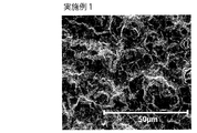
- FIG. 2 is a photograph of the surface of the tantalum carbide layer of the silicon carbide-tantalum carbide composite material obtained in Example 1.
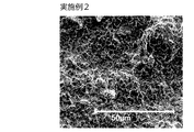
- FIG. 3 is a photograph of the surface of the tantalum carbide layer of the silicon carbide-tantalum carbide composite material obtained in Example 2.
- 4 is a photograph of the surface of the tantalum carbide layer of the silicon carbide-tantalum carbide composite material obtained in Example 3.
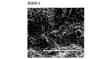
- FIG. FIG. 5 is a photograph of the surface of the tantalum carbide layer of the silicon carbide-tantalum carbide composite material obtained in Example 4.
- FIG. 1 is a schematic cross-sectional view of a silicon carbide-tantalum carbide composite material according to an embodiment of the first aspect and the second aspect of the present invention.
- FIG. 2 is a photograph of the surface of the tantalum carb
- the silicon carbide-tantalum carbide composite material 1 can be used as a susceptor used in, for example, a semiconductor manufacturing process.
- a semiconductor can be manufactured by placing a wafer or the like in the recess 1a of the silicon carbide-tantalum carbide composite material 1.
- the silicon carbide-tantalum carbide composite material is not limited to one used as a susceptor, and can be used for various applications. Further, the shape of the silicon carbide-tantalum carbide composite material can be designed as appropriate, and for example, it may not have a recess.
- the graphite substrate 11 is substantially composed of graphite.
- the graphite substrate 11 may contain components other than graphite such as boron.
- the thickness of the first silicon carbide layer 12 is not particularly limited. In order to improve the durability of the silicon carbide-tantalum carbide composite material 1, the thickness of the first silicon carbide layer 12 is preferably 60 ⁇ m or more, and more preferably 80 ⁇ m or more. The thickness of first silicon carbide layer 12 is preferably 200 ⁇ m or less.
- the first silicon carbide layer 12 is substantially composed of silicon carbide.
- a tantalum carbide layer 20 is disposed on the first silicon carbide layer 12. Specifically, the tantalum carbide layer 20 is disposed on the first silicon carbide layer 12 in the recess formed in the main body 10.
- the tantalum carbide layer 20 is substantially composed of tantalum carbide.
- the thickness of the tantalum carbide layer 20 is preferably 0.1 ⁇ m or more, and more preferably 1 ⁇ m or more.
- the thickness of the tantalum carbide layer 20 is preferably 10 ⁇ m or less.
- a second silicon carbide layer 13 is disposed between the tantalum carbide layer 20 and the first silicon carbide layer 12. Specifically, in the recess 1 a of the silicon carbide-tantalum carbide composite material 1, the second silicon carbide layer 13 is disposed between the tantalum carbide layer 20 and the first silicon carbide layer 12. More specifically, the second silicon carbide layer 13 is disposed immediately above the surface 12 a of the first silicon carbide layer 12, and the tantalum carbide layer 20 is directly above the surface 13 a of the second silicon carbide layer 13. It is arranged.
- the second silicon carbide layer 13 functions as an adhesion layer that causes the tantalum carbide layer 20 and the first silicon carbide layer 12 to adhere to each other.
- the peak intensity ratio G / D of the G band and D band of carbon measured by Raman spectroscopy is 1.0 or more, and preferably 1.1 or more.
- the silicon carbide-tantalum carbide composite material 1 has excellent durability.
- the details of the reason are not necessarily clear, but can be considered as follows, for example.
- the thermal expansion coefficients of silicon carbide and tantalum carbide are greatly different, the silicon carbide layer and the tantalum carbide layer are generally easily separated when subjected to a temperature change.
- tantalum and carbon contained in tantalum carbide form a strong bond.
- the crystallite diameter of the silicon carbide constituting the second silicon carbide layer 13 is preferably 753 mm or less, and preferably 740 mm or less. More preferred. This is because the crystallite diameter is reduced and the anchor effect between the second silicon carbide layer 13 and the tantalum carbide layer 20 is increased by reducing the proportion of silicon in the second silicon carbide layer 13. It is thought that. In addition, it is preferable that the crystallite diameter of the silicon carbide which comprises the 2nd silicon carbide layer 13 is 600 or more.
- the silicon carbide-tantalum carbide composite material 1 can be manufactured, for example, as follows. First, the graphite base material 11 is prepared. Next, the first silicon carbide layer 12 is formed on the surface 11a of the graphite substrate 11 by a method such as thermal CVD. Next, X-ray photoelectron spectroscopy is performed by subjecting at least a part of the surface of the first silicon carbide layer 12 to an etching process using H 2 gas, Cl 2 gas or the like, or a thermal carbonization process.
- the G / D ratio was measured by Raman spectroscopy, using an Ar laser with a wavelength of 532 nm, and a Microscope Raman spectrometer (Almega dispersion type laser Raman photometer) manufactured by Thermo Fisher Scientific. Further, when measured with SEM (JSM-6510LA manufactured by JEOL Ltd.), the thickness of the second silicon carbide layer 13 was 0.05 ⁇ m. The crystallite diameter of the second silicon carbide layer 13 was measured by XRD (RINT-Ultima III, manufactured by Rigaku) and found to be 641.0 mm.
- the resulting tantalum layer was carburized to obtain a silicon carbide-tantalum carbide composite material in which a tantalum carbide layer 20 having a thickness of 5 ⁇ m was formed.
- the carburizing process was performed as follows.
- Example 2 A silicon carbide-tantalum carbide composite material is obtained in the same manner as in Example 1 except that in the etching process of the first silicon carbide layer 12, a Cl 2 etching process using Cl 2 gas instead of H 2 gas is performed. Was made. After the etching treatment, the C / Si composition ratio measured by X-ray photoelectron spectroscopy of the second silicon carbide layer 13 was 1.36. The peak intensity ratio G / D of the G band and D band of the carbon measured by the Raman spectroscopy of the second silicon carbide layer 13 was 4.03. The crystallite diameter of the second silicon carbide layer 13 was 663.9 mm. The results are shown in Table 1. A surface photograph of the tantalum carbide layer 20 of the silicon carbide-tantalum carbide composite material obtained in Example 2 is shown in FIG. As is clear from FIG. 3, no cracks or peeling were observed on the surface of the tantalum carbide layer 20.
- Example 4 A silicon carbide-tantalum carbide composite material was produced in the same manner as in Example 1 except that the first silicon carbide layer 12 was subjected to thermal carbonization instead of etching.
- the thermal carbonization treatment was performed as follows. The silicon carbide-tantalum carbide composite material is placed under a reduced pressure of 10 ⁇ 4 Pa or less, and heated at about 1800 ° C. for 0.5 hour, whereby the first carbonization formed in the concave portion of the silicon carbide-tantalum carbide composite material. A part of Si was sublimated from the silicon layer 12 to form a second silicon carbide layer 13. After the thermal carbonization treatment, the C / Si composition ratio measured by X-ray photoelectron spectroscopy of the second silicon carbide layer 13 was 5.39.
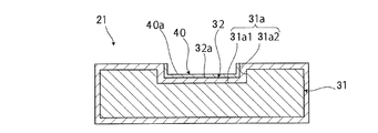
- the susceptor 21 includes a base material 31, a tantalum carbide layer 40, and a silicon carbide layer 32.
- SYMBOLS 1 Silicon carbide-tantalum carbide composite material 10 ... Main body 11 ... Graphite base material 11a ... Surface of graphite base material 12 ... First silicon carbide layer 12a ... Surface of first silicon carbide layer 13 ... Second silicon carbide layer 13a ... surface 20 of second silicon carbide layer 20 ... tantalum carbide layer 20a ... surface 21 of tantalum carbide layer ... susceptor 31 ... substrate 31a ... recess 31a1 of substrate ... bottom surface 31a2 of substrate recess ... Side surface 32 ... Silicon carbide layer 32a ... Silicon carbide layer surface 40 ... Tantalum carbide layer 40a ... Tantalum carbide layer surface
Landscapes
- Chemical & Material Sciences (AREA)
- Engineering & Computer Science (AREA)
- Ceramic Engineering (AREA)
- Materials Engineering (AREA)
- Organic Chemistry (AREA)
- Structural Engineering (AREA)
- Metallurgy (AREA)
- Inorganic Chemistry (AREA)
- Crystallography & Structural Chemistry (AREA)
- Chemical Kinetics & Catalysis (AREA)
- Mechanical Engineering (AREA)
- General Chemical & Material Sciences (AREA)
- Manufacturing & Machinery (AREA)
- Chemical Vapour Deposition (AREA)
- Container, Conveyance, Adherence, Positioning, Of Wafer (AREA)
- Crystals, And After-Treatments Of Crystals (AREA)
- Carbon And Carbon Compounds (AREA)
Abstract
Description
図1は、本実施形態に係る炭化ケイ素-炭化タンタル複合材を示す略図的断面図である。図1を参照しながら、本実施形態に係る炭化ケイ素-炭化タンタル複合材1の構成について説明する。
炭化ケイ素-炭化タンタル複合材1は、例えば、以下のようにして製造することができる。まず、黒鉛基材11を準備する。次に、黒鉛基材11の表面11a上に、熱CVDなどの方法によって、第1の炭化ケイ素層12を形成する。次に、第1の炭化ケイ素層12の表面の少なくとも一部を、H2ガス、Cl2ガスなどを用いたエッチング処理を行ったり、熱炭化処理を行ったりすることにより、X線光電子分光法によって測定されるC/Si組成比が1.2以上の第2の炭化ケイ素層13、またはラマン分光法によって測定される炭素のGバンド及びDバンドのピーク強度比G/Dが、1.0以上の第2の炭化ケイ素層13を形成する。次に、第2の炭化ケイ素層13の表面13aの上に、化学蒸着(CVD)法などによって、タンタル層を形成する。その後、タンタル層に浸炭処理を施すことにより、炭化タンタル層20を形成する。以上のような方法により、炭化ケイ素-炭化タンタル複合材1を製造することができる。なお、浸炭処理は、例えば、特開2010-280948号公報に記載された方法などの公知の方法により行うことができる。
以下のようにして炭化ケイ素-炭化タンタル複合材1と実質的に同様の構成を有する炭化ケイ素-炭化タンタル複合材を作製した。
キャリアガス:アルゴン
温度:1000℃
圧力:200Pa
第1の炭化ケイ素層12のエッチング処理において、H2ガスの代わりにCl2ガスを用いたCl2エッチング処理を行ったこと以外は、実施例1と同様にして、炭化ケイ素-炭化タンタル複合材を作製した。エッチング処理後において、第2の炭化ケイ素層13のX線光電子分光法によって測定したC/Si組成比は、1.36であった。また、第2の炭化ケイ素層13のラマン分光法によって測定される炭素のGバンド及びDバンドのピーク強度比G/Dは、4.03であった。第2の炭化ケイ素層13の結晶子径は、663.9Åであった。結果を表1に示す。実施例2で得られた炭化ケイ素-炭化タンタル複合材の炭化タンタル層20の表面写真を図3に示す。図3から明らかなとおり、炭化タンタル層20の表面には、クラックや剥離などが観察されなかった。
Cl2ガスの流通時間を2時間とした以外は、実施例2と同様にして、炭化ケイ素-炭化タンタル複合材を作製した。熱炭化処理後において、第2の炭化ケイ素層13のX線光電子分光法によって測定したC/Si組成比は、2.12であった。第2の炭化ケイ素層13の結晶子径は、739.6Åであった。また、第2の炭化ケイ素層13のラマン分光法によって測定される炭素のGバンド及びDバンドのピーク強度比G/Dは、5.88であった。結果を表1に示す。実施例3で得られた炭化ケイ素-炭化タンタル複合材の炭化タンタル層20の表面写真を図4に示す。図4から炭化タンタル層20の表面には、僅かにクラックが観察されるものの、実用上問題とならない程度であった。
第1の炭化ケイ素層12をエッチング処理する代わりに、熱炭化処理したこと以外は、実施例1と同様にして、炭化ケイ素-炭化タンタル複合材を作製した。熱炭化処理は、次のようにして行った。炭化ケイ素-炭化タンタル複合材を、10-4Pa以下の減圧下に置き、約1800℃で0.5時間加熱することにより、炭化ケイ素-炭化タンタル複合材の凹部に形成された第1の炭化ケイ素層12からSiの一部を昇華させて、第2の炭化ケイ素層13を形成した。熱炭化処理後において、第2の炭化ケイ素層13のX線光電子分光法によって測定したC/Si組成比は、5.39であった。また、第2の炭化ケイ素層13のラマン分光法によって測定される炭素のGバンド及びDバンドのピーク強度比G/Dは、7.20であった。第2の炭化ケイ素層13の結晶子径は、751.3Åであった。結果を表1に示す。実施例4で得られた炭化ケイ素-炭化タンタル複合材の炭化タンタル層20の表面写真を図5に示す。図5から炭化タンタル層20の表面には、僅かにクラックが観察されるものの、実用上問題とならない程度であった。
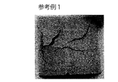
第1の炭化ケイ素層12のエッチング処理を行わなかったこと以外は、実施例1と同様にして、炭化ケイ素-炭化タンタル複合材を得た。なお、第1の炭化ケイ素層のX線光電子分光法によって測定したC/Si組成比は、1.1であった。また、第1の炭化ケイ素層のラマン分光法によって測定される炭素のGバンド及びDバンドのピーク強度比G/Dは、0であった。第2の炭化ケイ素層の結晶子径は、757.7Åであった。参考例1で得られた炭化ケイ素-炭化タンタル複合材の炭化タンタル層の表面写真を図6に示す。図6から明らかなとおり、炭化タンタル層の表面には、クラック及び剥離が観察された。

10…本体
11…黒鉛基材
11a…黒鉛基材の表面
12…第1の炭化ケイ素層
12a…第1の炭化ケイ素層の表面
13…第2の炭化ケイ素層
13a…第2の炭化ケイ素層の表面
20…炭化タンタル層
20a…炭化タンタル層の表面
21…サセプタ
31…基材
31a…基材の凹部
31a1…基材の凹部の底面
31a2…基材の凹部の側面
32…炭化ケイ素層
32a…炭化ケイ素層の表面
40…炭化タンタル層
40a…炭化タンタル層の表面
Claims (14)
- 表層の少なくとも一部が第1の炭化ケイ素層により構成された本体と、
前記第1の炭化ケイ素層の上に配された炭化タンタル層と、
前記炭化タンタル層と前記第1の炭化ケイ素層との間に配された第2の炭化ケイ素層と、を備え、
前記第2の炭化ケイ素層は、X線光電子分光法によって測定されるC/Si組成比が1.2以上であることを特徴とする炭化ケイ素-炭化タンタル複合材。 - 前記第2の炭化ケイ素層のX線光電子分光法によって測定されるC/Si組成比が、6.0以下である、請求項1に記載の炭化ケイ素-炭化タンタル複合材。
- 表層の少なくとも一部が第1の炭化ケイ素層により構成された本体と、
前記第1の炭化ケイ素層の上に配された炭化タンタル層と、
前記炭化タンタル層と前記第1の炭化ケイ素層との間に配された第2の炭化ケイ素層と、を備え、
前記第2の炭化ケイ素層は、ラマン分光法によって測定される炭素のGバンド及びDバンドのピーク強度比G/Dが、1.0以上であることを特徴とする炭化ケイ素-炭化タンタル複合材。 - 前記第2の炭化ケイ素層のラマン分光法によって測定される炭素のGバンド及びDバンドのピーク強度比G/Dが、7.5以下である、請求項3に記載の炭化ケイ素-炭化タンタル複合材。
- 前記第2の炭化ケイ素層の結晶子径は、753Å以下である、請求項1~4のいずれか1項に記載の炭化ケイ素-炭化タンタル複合材。
- 前記本体は、黒鉛基材と、前記黒鉛基材の上に配された前記第1の炭化ケイ素層とを備える、請求項1~5のいずれか1項に記載の炭化ケイ素-炭化タンタル複合材。
- 前記第2の炭化ケイ素層の厚みが、0.05μm以上である、請求項1~6のいずれか1項に記載の炭化ケイ素-炭化タンタル複合材。
- 請求項1~7のいずれか一項に記載の炭化ケイ素-炭素複合材を備え、
底面及び側面の少なくとも一方が前記炭化タンタル層により構成された凹部を有する、
サセプタ。 - 凹部を有する基材と、
前記凹部の底面上に配された炭化タンタル層と、
を備えたサセプタであって、
前記炭化タンタル層と前記基材との間に配された炭化ケイ素層をさらに備えることを特徴とする、サセプタ。 - 前記凹部の底面上において、前記炭化ケイ素層が、前記炭化タンタル層よりも厚い、請求項9に記載のサセプタ。
- 前記凹部の底面上における前記炭化ケイ素層の厚みが、60μm以上である、請求項9または10に記載のサセプタ。
- 前記凹部の底面上における前記炭化タンタル層の厚みが、10μm以下である、請求項9~11のいずれか1項に記載のサセプタ。
- 前記炭化タンタル層が前記凹部の側面の上にも配されており、
前記凹部の側面上において、前記炭化ケイ素層が前記炭化タンタル層と前記基材との間に配されている、請求項9~12のいずれか1項に記載のサセプタ。 - 前記基材が、黒鉛により構成されている、請求項9~13のいずれか1項に記載のサセプタ。
Priority Applications (5)
| Application Number | Priority Date | Filing Date | Title |
|---|---|---|---|
| KR1020157016688A KR102239607B1 (ko) | 2013-02-06 | 2014-01-28 | 탄화규소-탄화탄탈 복합재 및 서셉터 |
| CN201480007718.1A CN104968634B (zh) | 2013-02-06 | 2014-01-28 | 碳化硅‑碳化钽复合材料和基座 |
| US14/652,210 US9764992B2 (en) | 2013-02-06 | 2014-01-28 | Silicon carbide-tantalum carbide composite and susceptor |
| JP2014560729A JP6196246B2 (ja) | 2013-02-06 | 2014-01-28 | 炭化ケイ素−炭化タンタル複合材及びサセプタ |
| EP14748688.0A EP2955167B1 (en) | 2013-02-06 | 2014-01-28 | Silicon carbide-tantalum carbide composite and susceptor |
Applications Claiming Priority (6)
| Application Number | Priority Date | Filing Date | Title |
|---|---|---|---|
| JP2013-021167 | 2013-02-06 | ||
| JP2013021168 | 2013-02-06 | ||
| JP2013-021166 | 2013-02-06 | ||
| JP2013021166 | 2013-02-06 | ||
| JP2013021167 | 2013-02-06 | ||
| JP2013-021168 | 2013-02-06 |
Publications (1)
| Publication Number | Publication Date |
|---|---|
| WO2014123036A1 true WO2014123036A1 (ja) | 2014-08-14 |
Family
ID=51299633
Family Applications (1)
| Application Number | Title | Priority Date | Filing Date |
|---|---|---|---|
| PCT/JP2014/051821 Ceased WO2014123036A1 (ja) | 2013-02-06 | 2014-01-28 | 炭化ケイ素-炭化タンタル複合材及びサセプタ |
Country Status (7)
| Country | Link |
|---|---|
| US (1) | US9764992B2 (ja) |
| EP (1) | EP2955167B1 (ja) |
| JP (1) | JP6196246B2 (ja) |
| KR (1) | KR102239607B1 (ja) |
| CN (1) | CN104968634B (ja) |
| TW (1) | TWI585247B (ja) |
| WO (1) | WO2014123036A1 (ja) |
Cited By (10)
| Publication number | Priority date | Publication date | Assignee | Title |
|---|---|---|---|---|
| WO2015198798A1 (ja) * | 2014-06-24 | 2015-12-30 | 東洋炭素株式会社 | サセプタ及びその製造方法 |
| WO2017188145A1 (ja) * | 2016-04-26 | 2017-11-02 | 株式会社ブリヂストン | サセプタ |
| WO2018207942A1 (ja) * | 2017-05-12 | 2018-11-15 | 東洋炭素株式会社 | サセプタ、エピタキシャル基板の製造方法、及びエピタキシャル基板 |
| CN111748793A (zh) * | 2019-03-29 | 2020-10-09 | 株式会社爱发科 | 电热丝、电热丝的制造方法以及真空处理装置 |
| JP2021066650A (ja) * | 2019-10-22 | 2021-04-30 | エスケイシー・カンパニー・リミテッドSkc Co., Ltd. | 炭化珪素インゴット、その製造方法及び炭化珪素ウエハの製造方法 |
| JP2021070622A (ja) * | 2019-10-29 | 2021-05-06 | エスケイシー・カンパニー・リミテッドSkc Co., Ltd. | 炭化珪素ウエハ及び炭化珪素ウエハの製造方法 |
| JP2021187727A (ja) * | 2020-05-29 | 2021-12-13 | エスケイシー・カンパニー・リミテッドSkc Co., Ltd. | ウエハの製造方法、エピタキシャルウエハの製造方法、これによって製造されたウエハ及びエピタキシャルウエハ |
| JP2022068036A (ja) * | 2020-10-21 | 2022-05-09 | イビデン株式会社 | SiCの気相成長装置用部材及び気相成長装置用部材の再生方法 |
| US11359306B2 (en) | 2019-10-29 | 2022-06-14 | Senic Inc. | Method for preparing a SiC ingot and device for preparing a SiC ingot wherein electrical resistance of crucible body is 2.9 ohms or more |
| CN117836257A (zh) * | 2021-08-03 | 2024-04-05 | 弗劳恩霍夫应用研究促进协会 | 用于制备涂层基材的方法、涂层基材和其用途 |
Families Citing this family (14)
| Publication number | Priority date | Publication date | Assignee | Title |
|---|---|---|---|---|
| US9695944B2 (en) * | 2013-12-23 | 2017-07-04 | Flowserve Management Company | Electrical corrosion resistant mechanical seal |
| KR101824883B1 (ko) * | 2016-05-25 | 2018-02-02 | 주식회사 티씨케이 | 탄화탄탈 코팅 탄소 재료 |
| KR102051668B1 (ko) | 2016-12-20 | 2019-12-04 | 주식회사 티씨케이 | SiC 증착층을 포함하는 반도체 제조용 부품 및 그 제조방법 |
| KR102040378B1 (ko) * | 2016-12-20 | 2019-11-05 | 주식회사 티씨케이 | 지그를 이용한 반도체 제조용 부품의 제조방법 및 제조장치 |
| KR102785068B1 (ko) * | 2019-05-27 | 2025-03-20 | 슝크 싸이카브 테크놀로지 비.브이. | 화학 기상 증착 챔버 물품 |
| KR102211935B1 (ko) * | 2020-02-13 | 2021-02-04 | (주) 데크카본 | 레이다 파 흡수재 및 이를 제조하는 방법 |
| WO2021163664A1 (en) * | 2020-02-13 | 2021-08-19 | Jabil Inc. | Apparatus, system and method for providing a substrate chuck |
| US20220076988A1 (en) * | 2020-09-10 | 2022-03-10 | Applied Materials, Inc. | Back side design for flat silicon carbide susceptor |
| US20220411959A1 (en) * | 2021-06-24 | 2022-12-29 | Coorstek Kk | Susceptor and manufacturing method thereof |
| US20230009692A1 (en) * | 2021-07-07 | 2023-01-12 | Applied Materials, Inc | Coated substrate support assembly for substrate processing |
| KR102558286B1 (ko) * | 2022-07-21 | 2023-07-25 | 주식회사 엘엠케이 | 구리 연속 증착 소스 |
| JP2024119187A (ja) | 2023-02-22 | 2024-09-03 | アズビル株式会社 | バルブメンテナンス支援装置および支援方法 |
| JP2025123784A (ja) | 2024-02-13 | 2025-08-25 | アズビル株式会社 | 無線式開度計、バルブメンテナンス支援システムおよび支援方法 |
| CN119956319B (zh) * | 2025-03-28 | 2025-09-23 | 武汉理工大学 | 一种在碳基基底原位生长抗热震碳化钽涂层的方法 |
Citations (8)
| Publication number | Priority date | Publication date | Assignee | Title |
|---|---|---|---|---|
| JP2004084057A (ja) * | 2002-06-28 | 2004-03-18 | Ibiden Co Ltd | 炭素複合材料 |
| JP2006041358A (ja) * | 2004-07-29 | 2006-02-09 | Shindengen Electric Mfg Co Ltd | サセプタおよび化学気相成長方法 |
| JP2006060195A (ja) | 2004-07-22 | 2006-03-02 | Toyo Tanso Kk | サセプタ |
| WO2006085635A1 (ja) * | 2005-02-14 | 2006-08-17 | Toyo Tanso Co., Ltd. | 炭化タンタル被覆炭素材料およびその製造方法 |
| JP2010030846A (ja) * | 2008-07-30 | 2010-02-12 | Kyocera Corp | 窒化物体の製造方法 |
| JP2010280948A (ja) | 2009-06-04 | 2010-12-16 | Toyo Tanso Kk | タンタル部材の浸炭処理方法及びタンタル部材 |
| JP2011153045A (ja) * | 2010-01-28 | 2011-08-11 | Kyocera Corp | 単結晶体の製造方法 |
| JP2013254853A (ja) * | 2012-06-07 | 2013-12-19 | Mitsubishi Electric Corp | 基板支持体、半導体製造装置 |
Family Cites Families (4)
| Publication number | Priority date | Publication date | Assignee | Title |
|---|---|---|---|---|
| JP3963068B2 (ja) * | 2000-07-19 | 2007-08-22 | 豊田合成株式会社 | Iii族窒化物系化合物半導体素子の製造方法 |
| CN101001978B (zh) * | 2004-07-22 | 2010-10-13 | 东洋炭素株式会社 | 衬托器 |
| FR2925044B1 (fr) * | 2007-12-13 | 2010-03-12 | Snecma Propulsion Solide | Procede de realisation d'une couche de carbure refractaire sur une piece en materiau composite c/c. |
| CN101445392B (zh) * | 2008-12-31 | 2012-05-30 | 中南大学 | 一种石墨基体无裂纹TaC涂层及其制造方法 |
-
2014
- 2014-01-28 JP JP2014560729A patent/JP6196246B2/ja active Active
- 2014-01-28 EP EP14748688.0A patent/EP2955167B1/en active Active
- 2014-01-28 CN CN201480007718.1A patent/CN104968634B/zh active Active
- 2014-01-28 US US14/652,210 patent/US9764992B2/en active Active
- 2014-01-28 KR KR1020157016688A patent/KR102239607B1/ko active Active
- 2014-01-28 WO PCT/JP2014/051821 patent/WO2014123036A1/ja not_active Ceased
- 2014-02-05 TW TW103103723A patent/TWI585247B/zh active
Patent Citations (8)
| Publication number | Priority date | Publication date | Assignee | Title |
|---|---|---|---|---|
| JP2004084057A (ja) * | 2002-06-28 | 2004-03-18 | Ibiden Co Ltd | 炭素複合材料 |
| JP2006060195A (ja) | 2004-07-22 | 2006-03-02 | Toyo Tanso Kk | サセプタ |
| JP2006041358A (ja) * | 2004-07-29 | 2006-02-09 | Shindengen Electric Mfg Co Ltd | サセプタおよび化学気相成長方法 |
| WO2006085635A1 (ja) * | 2005-02-14 | 2006-08-17 | Toyo Tanso Co., Ltd. | 炭化タンタル被覆炭素材料およびその製造方法 |
| JP2010030846A (ja) * | 2008-07-30 | 2010-02-12 | Kyocera Corp | 窒化物体の製造方法 |
| JP2010280948A (ja) | 2009-06-04 | 2010-12-16 | Toyo Tanso Kk | タンタル部材の浸炭処理方法及びタンタル部材 |
| JP2011153045A (ja) * | 2010-01-28 | 2011-08-11 | Kyocera Corp | 単結晶体の製造方法 |
| JP2013254853A (ja) * | 2012-06-07 | 2013-12-19 | Mitsubishi Electric Corp | 基板支持体、半導体製造装置 |
Cited By (23)
| Publication number | Priority date | Publication date | Assignee | Title |
|---|---|---|---|---|
| WO2015198798A1 (ja) * | 2014-06-24 | 2015-12-30 | 東洋炭素株式会社 | サセプタ及びその製造方法 |
| JP2016008319A (ja) * | 2014-06-24 | 2016-01-18 | 東洋炭素株式会社 | サセプタ及びその製造方法 |
| US10522386B2 (en) | 2014-06-24 | 2019-12-31 | Toyo Tanso Co., Ltd. | Susceptor and method for manufacturing same |
| WO2017188145A1 (ja) * | 2016-04-26 | 2017-11-02 | 株式会社ブリヂストン | サセプタ |
| WO2018207942A1 (ja) * | 2017-05-12 | 2018-11-15 | 東洋炭素株式会社 | サセプタ、エピタキシャル基板の製造方法、及びエピタキシャル基板 |
| JPWO2018207942A1 (ja) * | 2017-05-12 | 2020-03-12 | 東洋炭素株式会社 | サセプタ、エピタキシャル基板の製造方法、及びエピタキシャル基板 |
| JP7233361B2 (ja) | 2017-05-12 | 2023-03-06 | 東洋炭素株式会社 | サセプタ、エピタキシャル基板の製造方法、及びエピタキシャル基板 |
| CN111748793B (zh) * | 2019-03-29 | 2022-08-09 | 株式会社爱发科 | 电热丝、电热丝的制造方法以及真空处理装置 |
| CN111748793A (zh) * | 2019-03-29 | 2020-10-09 | 株式会社爱发科 | 电热丝、电热丝的制造方法以及真空处理装置 |
| JP7030260B2 (ja) | 2019-10-22 | 2022-03-07 | セニック・インコーポレイテッド | 炭化珪素インゴット、その製造方法及び炭化珪素ウエハの製造方法 |
| US11466383B2 (en) | 2019-10-22 | 2022-10-11 | Senic Inc. | Silicon carbide ingot, method of preparing the same, and method for preparing silicon carbide wafer |
| JP2021066650A (ja) * | 2019-10-22 | 2021-04-30 | エスケイシー・カンパニー・リミテッドSkc Co., Ltd. | 炭化珪素インゴット、その製造方法及び炭化珪素ウエハの製造方法 |
| JP2021070622A (ja) * | 2019-10-29 | 2021-05-06 | エスケイシー・カンパニー・リミテッドSkc Co., Ltd. | 炭化珪素ウエハ及び炭化珪素ウエハの製造方法 |
| JP7042995B2 (ja) | 2019-10-29 | 2022-03-29 | セニック・インコーポレイテッド | 炭化珪素ウエハ及び炭化珪素ウエハの製造方法 |
| US11708644B2 (en) | 2019-10-29 | 2023-07-25 | Senic Inc. | Method for preparing SiC ingot, method for preparing SiC wafer and the SiC wafer prepared therefrom |
| US11359306B2 (en) | 2019-10-29 | 2022-06-14 | Senic Inc. | Method for preparing a SiC ingot and device for preparing a SiC ingot wherein electrical resistance of crucible body is 2.9 ohms or more |
| US11939698B2 (en) | 2020-05-29 | 2024-03-26 | Senic Inc. | Wafer manufacturing method, epitaxial wafer manufacturing method, and wafer and epitaxial wafer manufactured thereby |
| JP2021187727A (ja) * | 2020-05-29 | 2021-12-13 | エスケイシー・カンパニー・リミテッドSkc Co., Ltd. | ウエハの製造方法、エピタキシャルウエハの製造方法、これによって製造されたウエハ及びエピタキシャルウエハ |
| JP7023543B2 (ja) | 2020-05-29 | 2022-02-22 | セニック・インコーポレイテッド | ウエハの製造方法、エピタキシャルウエハの製造方法、これによって製造されたウエハ及びエピタキシャルウエハ |
| JP2022068036A (ja) * | 2020-10-21 | 2022-05-09 | イビデン株式会社 | SiCの気相成長装置用部材及び気相成長装置用部材の再生方法 |
| JP7477424B2 (ja) | 2020-10-21 | 2024-05-01 | イビデン株式会社 | SiCの気相成長装置用部材及び気相成長装置用部材の再生方法 |
| CN117836257A (zh) * | 2021-08-03 | 2024-04-05 | 弗劳恩霍夫应用研究促进协会 | 用于制备涂层基材的方法、涂层基材和其用途 |
| JP2024526804A (ja) * | 2021-08-03 | 2024-07-19 | フラウンホッファー-ゲゼルシャフト ツァー フェーデルング デア アンゲバンテン フォルシュング エー ファー | 被覆基材を調製する方法、被覆基材、及びその使用 |
Also Published As
| Publication number | Publication date |
|---|---|
| KR102239607B1 (ko) | 2021-04-13 |
| CN104968634A (zh) | 2015-10-07 |
| JP6196246B2 (ja) | 2017-09-13 |
| KR20150114942A (ko) | 2015-10-13 |
| US20150321966A1 (en) | 2015-11-12 |
| EP2955167B1 (en) | 2018-07-25 |
| TWI585247B (zh) | 2017-06-01 |
| EP2955167A1 (en) | 2015-12-16 |
| EP2955167A4 (en) | 2016-10-26 |
| CN104968634B (zh) | 2018-04-10 |
| TW201435159A (zh) | 2014-09-16 |
| JPWO2014123036A1 (ja) | 2017-02-02 |
| US9764992B2 (en) | 2017-09-19 |
Similar Documents
| Publication | Publication Date | Title |
|---|---|---|
| JP6196246B2 (ja) | 炭化ケイ素−炭化タンタル複合材及びサセプタ | |
| US9145339B2 (en) | Material having a multilayer architecture and intended for being contacted with liquid silicon | |
| JP7011129B2 (ja) | 大口径炭化ケイ素単結晶インゴットの成長方法 | |
| JP4985625B2 (ja) | 炭化珪素単結晶の製造方法 | |
| WO2010023934A1 (ja) | グラフェン/SiC複合材料の製造方法及びそれにより得られるグラフェン/SiC複合材料 | |
| CN112374912A (zh) | 一种碳化硅涂层石墨基座的制备方法 | |
| CN107344868B (zh) | 一种在SiC衬底上制备无缓冲层的单层石墨烯的方法 | |
| JP3680281B2 (ja) | タンタルの炭化物、タンタルの炭化物の製造方法、タンタルの炭化物配線、タンタルの炭化物電極 | |
| RU2684128C1 (ru) | Изделие с покрытием из карбида кремния и способ изготовления изделия с покрытием из карбида кремния | |
| KR102058870B1 (ko) | 대구경 탄화규소 단결정 잉곳의 성장방법 | |
| JP4916479B2 (ja) | 炭化珪素エピタキシャル用基板の製造方法 | |
| TWI551717B (zh) | 類鑽碳膜之製造方法 | |
| CN116200822A (zh) | 晶圆承载盘及其制备方法 | |
| JP2002097092A (ja) | SiC膜被覆ガラス状炭素材およびその製造方法 | |
| JP3617676B2 (ja) | 炭化珪素成形体の製造方法 | |
| CN116240520A (zh) | 碳化硅-氮化硼-热解石墨复合加热片及制备方法和应用 | |
| JPH10209061A (ja) | 半導体拡散炉用の構成部材 | |
| KR20140087342A (ko) | 종자정 받침대 부착 방법 및 종자정 받침대를 이용한 단결정 성장 방법 | |
| JP2021017391A (ja) | 炭素複合部材 | |
| JP2021172542A (ja) | SiC被覆黒鉛部材の接合体及びその製造方法 | |
| KR100639790B1 (ko) | 비저항이 조절된 저온 발열 탄소재의 제조 방법 | |
| JP2002128580A (ja) | 高純度SiCコ−トカ−ボン材の製造方法 | |
| TW201604124A (zh) | 一種形成奈米片狀結構網絡在基材上的製備方法及其應用 | |
| Wang et al. | Field emissions of graphene films deposited on different substrates by CVD system | |
| KR20120052788A (ko) | 서셉터 및 이의 제조 방법 |
Legal Events
| Date | Code | Title | Description |
|---|---|---|---|
| 121 | Ep: the epo has been informed by wipo that ep was designated in this application |
Ref document number: 14748688 Country of ref document: EP Kind code of ref document: A1 |
|
| DPE1 | Request for preliminary examination filed after expiration of 19th month from priority date (pct application filed from 20040101) | ||
| ENP | Entry into the national phase |
Ref document number: 2014560729 Country of ref document: JP Kind code of ref document: A |
|
| WWE | Wipo information: entry into national phase |
Ref document number: 14652210 Country of ref document: US |
|
| ENP | Entry into the national phase |
Ref document number: 20157016688 Country of ref document: KR Kind code of ref document: A |
|
| WWE | Wipo information: entry into national phase |
Ref document number: 2014748688 Country of ref document: EP |
|
| NENP | Non-entry into the national phase |
Ref country code: DE |